EP3637118A1 - Soft error inspection method, soft error inspection device, and soft error inspection system - Google Patents
Soft error inspection method, soft error inspection device, and soft error inspection system Download PDFInfo
- Publication number
- EP3637118A1 EP3637118A1 EP17912622.2A EP17912622A EP3637118A1 EP 3637118 A1 EP3637118 A1 EP 3637118A1 EP 17912622 A EP17912622 A EP 17912622A EP 3637118 A1 EP3637118 A1 EP 3637118A1
- Authority
- EP
- European Patent Office
- Prior art keywords
- semiconductor device
- soft error
- error inspection
- time
- inspection method
- Prior art date
- Legal status (The legal status is an assumption and is not a legal conclusion. Google has not performed a legal analysis and makes no representation as to the accuracy of the status listed.)
- Granted
Links
Images





Classifications
-
- G—PHYSICS
- G01—MEASURING; TESTING
- G01R—MEASURING ELECTRIC VARIABLES; MEASURING MAGNETIC VARIABLES
- G01R31/00—Arrangements for testing electric properties; Arrangements for locating electric faults; Arrangements for electrical testing characterised by what is being tested not provided for elsewhere
- G01R31/26—Testing of individual semiconductor devices
- G01R31/265—Contactless testing
- G01R31/2653—Contactless testing using electron beams
-
- G—PHYSICS
- G01—MEASURING; TESTING
- G01R—MEASURING ELECTRIC VARIABLES; MEASURING MAGNETIC VARIABLES
- G01R31/00—Arrangements for testing electric properties; Arrangements for locating electric faults; Arrangements for electrical testing characterised by what is being tested not provided for elsewhere
- G01R31/26—Testing of individual semiconductor devices
- G01R31/265—Contactless testing
-
- G—PHYSICS
- G01—MEASURING; TESTING
- G01R—MEASURING ELECTRIC VARIABLES; MEASURING MAGNETIC VARIABLES
- G01R31/00—Arrangements for testing electric properties; Arrangements for locating electric faults; Arrangements for electrical testing characterised by what is being tested not provided for elsewhere
- G01R31/26—Testing of individual semiconductor devices
- G01R31/265—Contactless testing
- G01R31/2656—Contactless testing using non-ionising electromagnetic radiation, e.g. optical radiation
-
- G—PHYSICS
- G01—MEASURING; TESTING
- G01R—MEASURING ELECTRIC VARIABLES; MEASURING MAGNETIC VARIABLES
- G01R31/00—Arrangements for testing electric properties; Arrangements for locating electric faults; Arrangements for electrical testing characterised by what is being tested not provided for elsewhere
- G01R31/28—Testing of electronic circuits, e.g. by signal tracer
- G01R31/2851—Testing of integrated circuits [IC]
- G01R31/2855—Environmental, reliability or burn-in testing
- G01R31/2872—Environmental, reliability or burn-in testing related to electrical or environmental aspects, e.g. temperature, humidity, vibration, nuclear radiation
-
- G—PHYSICS
- G01—MEASURING; TESTING
- G01R—MEASURING ELECTRIC VARIABLES; MEASURING MAGNETIC VARIABLES
- G01R31/00—Arrangements for testing electric properties; Arrangements for locating electric faults; Arrangements for electrical testing characterised by what is being tested not provided for elsewhere
- G01R31/28—Testing of electronic circuits, e.g. by signal tracer
- G01R31/302—Contactless testing
- G01R31/305—Contactless testing using electron beams
- G01R31/307—Contactless testing using electron beams of integrated circuits
Definitions
- the present invention relates to a soft error inspection method, a soft error inspection apparatus, and a soft error inspection system.
- LSI large scale integration
- FA factory automation
- a soft error inspection method there are a running test in a high altitude, a test using an accelerator, and the like.
- the test using the accelerator can be further divided into a method of radiating neutrons or ions to the entire surface of an LSI chip, and a method of locally radiating focusable electrons or lasers.
- a laser evaluation method can be implemented with small-scale equipment because it does not need to make a vacuum, and is superior in that a specific memory area can be individually evaluated.
- Patent Document 1 Japanese National Publication of International Patent Application No. 2011-504581
- Non-Patent Document 1 J. R. Schwank, and et al., IEEE Trans. Nucl. Sci., 57 (2010) 1827 .
- a soft error inspection method for a semiconductor device includes: irradiating and scanning the semiconductor device with a laser beam or an electron beam; and measuring and storing a time of bit inversion for each of areas irradiated with the laser beam or the electron beam of the semiconductor device.
- the endurance time and the like can be known regarding the soft error of the semiconductor device.
- an energy beam is used to perform accelerated evaluation of the SEU, but generation mechanisms of the SEU are different from each other between a laser and charged particles such as an electron beam.
- the charged particles such as the electron beam
- an electron-hole pair is generated by the ionization effect by irradiating the LSI chip with the charged particles such as the electron beam.
- the laser when the LSI chip is irradiated with the laser beam, an electron-hole pair is generated by an excitation process in which two photons are simultaneously absorbed, which is referred to as two-photon absorption.
- the electron-hole pair is generated by indirect transition.
- generation mechanisms of the electron-hole pair are different from each other between the laser and the charged particles such as the electron beam, but processes of inducing the subsequent SEU are the same as each other.
- a soft error due to radiation of charged particles including electrons can be quantitatively evaluated by linear energy transfer (LET) (an index that represents quality of radiation by the amount of energy given per unit length).
- LET linear energy transfer
- Equation 1 Since irradiation by charged particle radiation and laser irradiation by two-photon absorption have a relationship of the equation indicated in Equation 1, for convenience, in the following description, description will be made as the LET.
- parameters of an irradiation condition of the laser and the charged particles such as the electron beam include energy, power, dosage rate, dose, frequency, pulse width, duty ratio, and the like.
- the LET given to a material changes as a result.
- the irradiation condition not only a total amount of energy given is a problem, but for example, a recovery phenomenon due to re-inversion phenomenon often occurs when bit inversion measurement is actually performed, and such a recovery phenomenon largely depends on the pulse width, the duty ratio, or the like. For that reason, recording bit information of the memory under various irradiation conditions is important for durability evaluation.
- the energy density of the laser is 0.02 J/cm 2
- the center wavelength is 1560 nm
- the power is 340 mW
- the frequency is 80 MHz, or the like.
- a laser focused to several micrometers by use of a laser optical system is radiated to an LSI chip that is a semiconductor device to be a sample.
- a scanning electron microscope (SEM) may be used.
- the laser or the charged particles such as the electron beam are radiated under a specific irradiation condition, at a certain coordinate position of the LSI chip, and a temporal change in the bit information of the memory of the LSI is recorded during the irradiation.
- a position is moved of the energy beam or the LSI chip that is the semiconductor device to be the sample, and similar processing is repeated.
- An acceleration factor of the laser irradiation or the electron beam irradiation to atmospheric radiation may be calculated under each irradiation condition by using a memory to be a standard sample in advance.
- a value of the acceleration factor can be calculated by collating error occurrence frequency.
- a durability (endurance time) map according to energy beam irradiation can be calculated by a product of an irradiation time taken for bit inversion and the acceleration factor. When the endurance time map is converted into an amount per unit time, it becomes an error occurrence frequency map.
- a memory operation method may then be adjusted not to cause a trouble as a semiconductor device.
- it may be determined whether or not the LSI chip being evaluated satisfies a specification of the error occurrence frequency.
- an error occurrence frequency area that does not satisfy the specification may be visualized by coloring or the like.
- the number of areas that do not satisfy the specification existing in the LSI chip may be counted to determine a durability grade of the LSI chip.
- memory allocation may be optimized depending on a use environment and the like.
- charges are generated around an incident position, so that it is considered that a memory near the incident position is likely to be inverted. For this reason, in the case of overall averaging, combinations may be adjusted such that positions (addresses) with low durability are not allocated together.
- adjustment may be made by combining only high durability addresses without using low durability addresses.
- FIG. 1 illustrates the soft error inspection apparatus and a soft error inspection system in the present embodiment.
- the soft error inspection apparatus in the present embodiment includes a scanning stage 20, an irradiation source 30, a scanning control unit 21, an irradiation control unit 31, a measuring instrument 40, a control unit 50, and the like.
- the control unit 50 includes an information processing unit 51, a storage unit 52, a display unit 53, an input unit 54, and the like.
- the semiconductor device 10 that is a sample to be inspected is an LSI chip or the like, and such a semiconductor device 10 is set on the scanning stage 20 and can be moved two-dimensionally, that is, in the X axis direction and the Y axis direction, by the scanning stage 20.
- the scanning stage 20 is controlled by the scanning control unit 21.
- the irradiation source 30 emits a laser beam radiated to the semiconductor device 10, and is controlled by the irradiation control unit 31.
- the laser beam is emitted from the irradiation source 30; however, the charged particles such as the electron beam may be emitted.
- the semiconductor device 10 is a semiconductor device formed of silicon
- a wavelength of the laser emitted from the irradiation source 30 is, for example, about 1500 nm.
- the measuring instrument 40 is a tester or the like, and is coupled to the terminal of the semiconductor device 10, and can measure a change in information stored in the semiconductor device 10.
- the control unit 50 performs control of the entire soft error inspection apparatus and information processing operation regarding the soft error inspection method in the present embodiment.
- the information processing unit 51 is connected to the storage unit 52 that stores information, the display unit 53 for displaying necessary information, and the input unit 54 for inputting information to the information processing unit 51, and the like.
- the soft error inspection system is enabled to execute the soft error inspection method described below by the control in the control unit 50.
- the semiconductor device 10 to be inspected in the soft error inspection method in the present embodiment is a static random access memory (SRAM), a flash memory, a field-programmable gate array (FPGA), an application specific integrated circuit (ASIC), or the like.
- SRAM static random access memory
- FPGA field-programmable gate array
- ASIC application specific integrated circuit
- an irradiation condition of the laser to be irradiated is set. Specifically, one or more irradiation conditions are selected in advance in consideration of parameters such as the LET, energy, dosage rate, dosage, pulse width, frequency, and duty ratio, and one of the selected irradiation conditions is set as the irradiation condition.
- the energy is energy of the laser.
- the dosage rate is also called flux, and is the number of photons per unit time and unit area.
- the dosage is also called a dose, and is the number of photons per unit area.
- the pulse width, frequency, and duty ratio respectively mean a pulse width of a laser pulse to be radiated, a frequency of the pulse, and a duty ratio of the pulse.
- step 104 the semiconductor device 10 to be a sample is irradiated with the laser beam for a predetermined time under the set irradiation condition. Specifically, as illustrated in FIG. 3 , the laser beam is radiated to a predetermined position of the semiconductor device 10 for the predetermined time under the set condition.
- step 106 time-series data of bit information of a position irradiated with the laser beam is measured, and stored in the storage unit 52 or the like.
- the time-series data of the bit information of the position irradiated with the laser beam that is, a temporal change of the bit information is measured and stored in the storage unit 52 or the like, by the measuring instrument 40 such as the tester, in a state where the laser beam is radiated.
- FIGs. 4A to 4C illustrate the time-series data of the bit information of the position irradiated with the laser beam detected by the measuring instrument 40.
- FIG. 4A illustrates a state where the bit information is inverted from 0 to 1 when time t 1 has elapsed from the laser beam irradiation start.
- FIG. 4B illustrates a state where the bit information is inverted from 0 to 1 when time t 2 has elapsed from the laser beam irradiation start.
- FIG. 4C illustrates a state where the bit information is inverted from 0 to 1 when time t 3 has elapsed from the laser beam irradiation start, and further, the bit information is re-inverted from 1 to 0 when time t 4 has elapsed.
- step 108 it is determined whether or not scanning by the laser beam has ended. Specifically, in the soft error inspection method in the present embodiment, since the inspection is performed by scanning a predetermined area of the semiconductor device 10, it is determined whether or not the scanning by the laser beam has ended in the semiconductor device 10, that is, whether or not the inspection of the predetermined area has ended. In a case where the scanning by the laser beam has ended, the processing proceeds to step 110, and in a case were the scanning by the laser beam has not ended, an irradiation position of the laser beam is moved, and the processing proceeds to step 104 and steps 104 and 106 are repeated.
- step 110 it is determined whether or not there is a next irradiation condition. Specifically, it is determined whether or not there is a measurement condition that has not been performed under the set irradiation conditions although one or a plurality of irradiation conditions is set in step 102. In a case where there is the next irradiation condition, the processing proceeds to step 102, and the next irradiation condition is set and steps 104 and 106 are repeated. In a case where there is no irradiation condition next, the processing proceeds to step 112.
- step 112 on the basis of an obtained result, a temporal change map is created of the bit information of the semiconductor device 10 under each irradiation condition. Specifically, as illustrated in FIG. 5 , the temporal change map of the bit information in three dimensions x, y, and t is created for each irradiation condition.
- step 114 an endurance time map is created. Specifically, as illustrated in FIG. 5 , an endurance time at each bit position is calculated by multiplication of a time required for inversion at each bit position by a predetermined acceleration factor, and the endurance time is two-dimensionalized, whereby the endurance time map is obtained as illustrated in FIG. 6 .
- step 116 on the basis of the endurance time map obtained in step 114, it is determined whether or not the semiconductor device 10 to be inspected satisfies a predetermined standard. For example, it is determined whether or not a ratio of an area with an endurance time of greater than or equal to five years is greater than or equal to 90%. In a case where the predetermined standard is satisfied, the processing proceeds to step 118, and in a case where the predetermined standard is not satisfied, an alert is issued and the semiconductor device 10 is treated as a defective product, and then the processing ends.
- a predetermined standard For example, it is determined whether or not a ratio of an area with an endurance time of greater than or equal to five years is greater than or equal to 90%.
- step 118 on the basis of the endurance time map, ranking is performed of the semiconductor device 10 inspected. Specifically, the ranking is performed such that, regarding a ratio of the area with the endurance time of greater than or equal to five years, in a case where the ratio is greater than or equal to 97%, the device is ranked as rank A, in a case where the ratio is less than 97% and greater than or equal to 94%, the device is ranked as rank B, and in a case where the ratio is less than 94% and greater than or equal to 90%, the device is ranked as rank C, and then the processing ends.
- the soft error inspection method in the present embodiment ends.
- the endurance time can be known regarding the soft error for each area of the semiconductor device, and quality determination or the like of the semiconductor device can be performed on the basis of the endurance time obtained.
- the soft error inspection method in the present embodiment is performed by using the soft error inspection apparatus in the first embodiment.
- an irradiation condition of the laser to be irradiated is set. Specifically, one or more irradiation conditions are selected in advance in consideration of the LET, energy, dosage rate, dosage, pulse width, frequency, duty ratio, and the like, and one of the selected irradiation conditions is set as the irradiation condition.
- step 204 the semiconductor device 10 to be a sample is irradiated with the laser beam for a predetermined time under the set irradiation condition.
- step 206 time-series data of bit information of a position irradiated with the laser beam is measured, and stored in the storage unit 52 or the like.
- step 208 it is determined whether or not scanning by the laser beam has ended. In a case where the scanning by the laser beam has ended, the processing proceeds to step 210, and in a case were the scanning by the laser beam has not ended, an irradiation position of the laser beam is moved, and the processing proceeds to step 204 and steps 204 and 206 are repeated.
- step 210 it is determined whether or not there is a next irradiation condition. In a case where there is the next irradiation condition, the processing proceeds to step 202, and the next irradiation condition is set and steps 204 and 206 are repeated. In a case where there is no irradiation condition next, the processing proceeds to step 212.
- step 212 on the basis of an obtained result, a temporal change map is created of the bit information of the semiconductor device 10 under each irradiation condition.
- step 214 radiation measurement is performed of an environment in which the semiconductor device 10 is used.
- an acceleration factor is calculated by comparing an amount of radiation of the environment in which the semiconductor device 10 is used obtained in step 214 is compared with the LET. For example, in a case where one second of laser irradiation time corresponds to one year (3.2 ⁇ 10 7 seconds) of radiation in the environment in which the semiconductor device is used, the acceleration factor is 3.2 ⁇ 10 7 .
- step 218 an endurance time map is created by using the acceleration factor obtained in step 216. Specifically, an endurance time at each bit position is calculated by multiplication of a time required for inversion at each bit position by the acceleration factor obtained in step 216, and the endurance time is two-dimensionalized, whereby the endurance time map is obtained.
- step 220 on the basis of the endurance time map obtained in step 218, it is determined whether or not the semiconductor device 10 that is a sample to be inspected satisfies a predetermined standard. In a case where the predetermined standard is satisfied, the processing proceeds to step 222, and in a case where the predetermined standard is not satisfied, the semiconductor device 10 becomes a defective product, and then the processing ends.
- step 222 obtained information regarding durability is stored in the semiconductor device.
- information regarding the endurance time map may be stored in a partial area 11a of a memory area 11 of the semiconductor device 10.
- memory allocation can be optimized in the semiconductor device 10 when the semiconductor device 10 is used.
- position information of a low tolerance area having a short endurance time or position information of a high tolerance area having a long endurance time may be stored in the partial area 11a of the memory area 11 of the semiconductor device 10.
- the position information of the low tolerance area, the high tolerance area, or the like may be stored outside the FPGA, that is, in a semiconductor device such as a flash memory or EEPROM that is an external storage medium.
- an area to be used may be set on the basis of the bit inversion time obtained above.
- the area to be used may be set corresponding to an elapsed time having been used and a purpose of use.
- bits of the high tolerance area having the long endurance time may be preferentially used, and the low tolerance areas may not be allocated consecutively.
- an allocated combination may be canceled and a combination may be made to prolong the endurance time.
- an area having a short endurance time may be avoided in use.
- Such allocation may be performed by a person using an apparatus on which the semiconductor device 10 is mounted, and a function of performing such allocation may be incorporated in the apparatus on which the semiconductor device 10 is mounted.
- the soft error inspection method in the present embodiment ends.
- the semiconductor device can be operated in consideration of the soft error, and highly reliable information processing can be performed.
Landscapes
- Physics & Mathematics (AREA)
- General Physics & Mathematics (AREA)
- Engineering & Computer Science (AREA)
- Computer Hardware Design (AREA)
- Microelectronics & Electronic Packaging (AREA)
- General Engineering & Computer Science (AREA)
- Health & Medical Sciences (AREA)
- Toxicology (AREA)
- Environmental & Geological Engineering (AREA)
- Electromagnetism (AREA)
- Tests Of Electronic Circuits (AREA)
- Testing Or Measuring Of Semiconductors Or The Like (AREA)
- Testing Of Individual Semiconductor Devices (AREA)
- For Increasing The Reliability Of Semiconductor Memories (AREA)
Abstract
Description
- The present invention relates to a soft error inspection method, a soft error inspection apparatus, and a soft error inspection system.
- In semiconductor devices such as large scale integration (LSI), it is known that a so-called soft error occurs that is a malfunction due to radiation. Such a soft error has become a problem in not only mission-critical devices such as infrastructure servers and supercomputers, but also apparatuses that require radiation resistance such as for space use and medical use, and apparatuses that cannot be stopped for 24 hours such as factory automation (FA) devices and communication base station equipment.
- In general, no defect remains of the soft error, so that inspection is difficult. Specifically, as a soft error inspection method, there are a running test in a high altitude, a test using an accelerator, and the like. The test using the accelerator can be further divided into a method of radiating neutrons or ions to the entire surface of an LSI chip, and a method of locally radiating focusable electrons or lasers. Among these methods, a laser evaluation method can be implemented with small-scale equipment because it does not need to make a vacuum, and is superior in that a specific memory area can be individually evaluated.
- Patent Document 1: Japanese National Publication of International Patent Application No.
2011-504581 - Non-Patent Document 1: J. R. Schwank, and et al., IEEE Trans. Nucl. Sci., 57 (2010) 1827.
- However, in the laser evaluation method, only an inverted position can be known of a memory that is inverted by radiation of a laser beam, but durability (endurance period) regarding the soft error cannot be known.
- There is therefore a need for a soft error inspection method capable of locally evaluating influence of radiation received by the semiconductor device, particularly the durability, and knowing an endurance time or the like regarding the soft error of the semiconductor device.
- According to one aspect of the present embodiment, a soft error inspection method for a semiconductor device includes: irradiating and scanning the semiconductor device with a laser beam or an electron beam; and measuring and storing a time of bit inversion for each of areas irradiated with the laser beam or the electron beam of the semiconductor device.
- According to the soft error inspection method disclosed, the endurance time and the like can be known regarding the soft error of the semiconductor device.
-
-
FIG. 1 is a structural diagram of a soft error inspection apparatus in a first embodiment. -
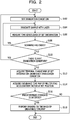
FIG. 2 is a flowchart of a soft error inspection method in the first embodiment. -
FIG. 3 is an explanatory diagram (1) of the soft error inspection method in the first embodiment. -
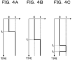
FIG. 4 is an explanatory diagram (2) of the soft error inspection method in the first embodiment. -
FIG. 5 is an explanatory diagram (3) of the soft error inspection method in the first embodiment. -
FIG. 6 is an explanatory diagram (4) of the soft error inspection method in the first embodiment. -
FIG. 7 is a flowchart of a soft error inspection method in a second embodiment. -
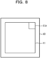
FIG. 8 is an explanatory diagram of a semiconductor device obtained in the second embodiment. -
FIG. 9 is an explanatory diagram of the soft error inspection method in the second embodiment. - Hereinafter, embodiments will be described. Note that, the same members and the like are denoted by the same reference numerals and repeated description will be omitted.
- First, an outline will be described of a soft error and a soft error inspection method. When a high energy beam is incident on the inside of an LSI chip, it continues to travel while losing energy, and an electron-hole pair is generated along its track. When these charges move to an electrode and flow into a storage node and become charges greater than or equal to a threshold value, bit information recorded until then is inverted (from 0 to 1, or from 1 to 0). This phenomenon is called single event upset (SEU) and is the largest malfunction factor of a memory in the LSI chip.
- As described later, in the present embodiment, an energy beam is used to perform accelerated evaluation of the SEU, but generation mechanisms of the SEU are different from each other between a laser and charged particles such as an electron beam. In the case of the charged particles such as the electron beam, an electron-hole pair is generated by the ionization effect by irradiating the LSI chip with the charged particles such as the electron beam. On the other hand, in the case of the laser, when the LSI chip is irradiated with the laser beam, an electron-hole pair is generated by an excitation process in which two photons are simultaneously absorbed, which is referred to as two-photon absorption. Specifically, when energy by the photon exceeds 1.12 eV that is the band gap energy of Si, the electron-hole pair is generated by indirect transition. As described above, generation mechanisms of the electron-hole pair are different from each other between the laser and the charged particles such as the electron beam, but processes of inducing the subsequent SEU are the same as each other.
- A soft error due to radiation of charged particles including electrons can be quantitatively evaluated by linear energy transfer (LET) (an index that represents quality of radiation by the amount of energy given per unit length). On the other hand, an energy threshold value P.E at which a soft error occurs due to two-photon absorption by the laser is expressed by an equation indicated in
Equation 1 below, by using the LET.
- Since irradiation by charged particle radiation and laser irradiation by two-photon absorption have a relationship of the equation indicated in
Equation 1, for convenience, in the following description, description will be made as the LET. - There are various parameters as parameters of an irradiation condition of the laser and the charged particles such as the electron beam, and examples thereof include energy, power, dosage rate, dose, frequency, pulse width, duty ratio, and the like. When these parameters of the irradiation condition are changed, the LET given to a material changes as a result. Regarding the irradiation condition, not only a total amount of energy given is a problem, but for example, a recovery phenomenon due to re-inversion phenomenon often occurs when bit inversion measurement is actually performed, and such a recovery phenomenon largely depends on the pulse width, the duty ratio, or the like. For that reason, recording bit information of the memory under various irradiation conditions is important for durability evaluation. Note that, as the irradiation condition, for example, the energy density of the laser is 0.02 J/cm2, the center wavelength is 1560 nm, the power is 340 mW, the frequency is 80 MHz, or the like.
- In the case of the laser irradiation, a laser focused to several micrometers by use of a laser optical system is radiated to an LSI chip that is a semiconductor device to be a sample. In addition, in the case of the electron beam irradiation, a scanning electron microscope (SEM) may be used. In either case, the laser or the charged particles such as the electron beam are radiated under a specific irradiation condition, at a certain coordinate position of the LSI chip, and a temporal change in the bit information of the memory of the LSI is recorded during the irradiation. After irradiation for a sufficient time in consideration of re-inversion and the like, a position is moved of the energy beam or the LSI chip that is the semiconductor device to be the sample, and similar processing is repeated.
- An acceleration factor of the laser irradiation or the electron beam irradiation to atmospheric radiation may be calculated under each irradiation condition by using a memory to be a standard sample in advance. A value of the acceleration factor can be calculated by collating error occurrence frequency. A durability (endurance time) map according to energy beam irradiation can be calculated by a product of an irradiation time taken for bit inversion and the acceleration factor. When the endurance time map is converted into an amount per unit time, it becomes an error occurrence frequency map.
- When these maps are obtained, a memory operation method may then be adjusted not to cause a trouble as a semiconductor device. Although various cases are assumed for the operation method, for example, it may be determined whether or not the LSI chip being evaluated satisfies a specification of the error occurrence frequency. At this time, an error occurrence frequency area that does not satisfy the specification may be visualized by coloring or the like. In addition, the number of areas that do not satisfy the specification existing in the LSI chip may be counted to determine a durability grade of the LSI chip.
- In addition, memory allocation may be optimized depending on a use environment and the like. When radiation is incident on the material, charges are generated around an incident position, so that it is considered that a memory near the incident position is likely to be inverted. For this reason, in the case of overall averaging, combinations may be adjusted such that positions (addresses) with low durability are not allocated together. In addition, adjustment may be made by combining only high durability addresses without using low durability addresses.
- Next, a soft error inspection apparatus in the first embodiment will be described.
FIG. 1 illustrates the soft error inspection apparatus and a soft error inspection system in the present embodiment. The soft error inspection apparatus in the present embodiment includes ascanning stage 20, anirradiation source 30, ascanning control unit 21, anirradiation control unit 31, a measuringinstrument 40, acontrol unit 50, and the like. Thecontrol unit 50 includes aninformation processing unit 51, astorage unit 52, adisplay unit 53, aninput unit 54, and the like. - The
semiconductor device 10 that is a sample to be inspected is an LSI chip or the like, and such asemiconductor device 10 is set on thescanning stage 20 and can be moved two-dimensionally, that is, in the X axis direction and the Y axis direction, by thescanning stage 20. Thescanning stage 20 is controlled by thescanning control unit 21. - The
irradiation source 30 emits a laser beam radiated to thesemiconductor device 10, and is controlled by theirradiation control unit 31. In the present embodiment, a case will be described where the laser beam is emitted from theirradiation source 30; however, the charged particles such as the electron beam may be emitted. In a case where thesemiconductor device 10 is a semiconductor device formed of silicon, since a wavelength range in which two-photon absorption occurs in silicon is 1100 nm to 2100 nm, a wavelength of the laser emitted from theirradiation source 30 is, for example, about 1500 nm. - The measuring
instrument 40 is a tester or the like, and is coupled to the terminal of thesemiconductor device 10, and can measure a change in information stored in thesemiconductor device 10. - The
control unit 50 performs control of the entire soft error inspection apparatus and information processing operation regarding the soft error inspection method in the present embodiment. Theinformation processing unit 51 is connected to thestorage unit 52 that stores information, thedisplay unit 53 for displaying necessary information, and theinput unit 54 for inputting information to theinformation processing unit 51, and the like. In the present embodiment, the soft error inspection system is enabled to execute the soft error inspection method described below by the control in thecontrol unit 50. - Next, the soft error inspection method in the present embodiment will be described with reference to
FIG. 2 . Thesemiconductor device 10 to be inspected in the soft error inspection method in the present embodiment is a static random access memory (SRAM), a flash memory, a field-programmable gate array (FPGA), an application specific integrated circuit (ASIC), or the like. - First, in step 102 (S102), an irradiation condition of the laser to be irradiated is set. Specifically, one or more irradiation conditions are selected in advance in consideration of parameters such as the LET, energy, dosage rate, dosage, pulse width, frequency, and duty ratio, and one of the selected irradiation conditions is set as the irradiation condition. Here, the energy is energy of the laser. The dosage rate is also called flux, and is the number of photons per unit time and unit area. The dosage is also called a dose, and is the number of photons per unit area. The pulse width, frequency, and duty ratio respectively mean a pulse width of a laser pulse to be radiated, a frequency of the pulse, and a duty ratio of the pulse.
- Next, in step 104 (S104), the
semiconductor device 10 to be a sample is irradiated with the laser beam for a predetermined time under the set irradiation condition. Specifically, as illustrated inFIG. 3 , the laser beam is radiated to a predetermined position of thesemiconductor device 10 for the predetermined time under the set condition. - Next, in step 106 (S106), time-series data of bit information of a position irradiated with the laser beam is measured, and stored in the
storage unit 52 or the like. Specifically, as illustrated inFIG. 3 , the time-series data of the bit information of the position irradiated with the laser beam, that is, a temporal change of the bit information is measured and stored in thestorage unit 52 or the like, by the measuringinstrument 40 such as the tester, in a state where the laser beam is radiated.FIGs. 4A to 4C illustrate the time-series data of the bit information of the position irradiated with the laser beam detected by the measuringinstrument 40.FIG. 4A illustrates a state where the bit information is inverted from 0 to 1 when time t1 has elapsed from the laser beam irradiation start.FIG. 4B illustrates a state where the bit information is inverted from 0 to 1 when time t2 has elapsed from the laser beam irradiation start.FIG. 4C illustrates a state where the bit information is inverted from 0 to 1 when time t3 has elapsed from the laser beam irradiation start, and further, the bit information is re-inverted from 1 to 0 when time t4 has elapsed. - Next, in step 108 (S108), it is determined whether or not scanning by the laser beam has ended. Specifically, in the soft error inspection method in the present embodiment, since the inspection is performed by scanning a predetermined area of the
semiconductor device 10, it is determined whether or not the scanning by the laser beam has ended in thesemiconductor device 10, that is, whether or not the inspection of the predetermined area has ended. In a case where the scanning by the laser beam has ended, the processing proceeds to step 110, and in a case were the scanning by the laser beam has not ended, an irradiation position of the laser beam is moved, and the processing proceeds to step 104 and steps 104 and 106 are repeated. - Next, in step 110 (S110), it is determined whether or not there is a next irradiation condition. Specifically, it is determined whether or not there is a measurement condition that has not been performed under the set irradiation conditions although one or a plurality of irradiation conditions is set in step 102. In a case where there is the next irradiation condition, the processing proceeds to step 102, and the next irradiation condition is set and steps 104 and 106 are repeated. In a case where there is no irradiation condition next, the processing proceeds to step 112.
- Next, in step 112 (S112), on the basis of an obtained result, a temporal change map is created of the bit information of the
semiconductor device 10 under each irradiation condition. Specifically, as illustrated inFIG. 5 , the temporal change map of the bit information in three dimensions x, y, and t is created for each irradiation condition. - Next, in step 114 (S114), an endurance time map is created. Specifically, as illustrated in
FIG. 5 , an endurance time at each bit position is calculated by multiplication of a time required for inversion at each bit position by a predetermined acceleration factor, and the endurance time is two-dimensionalized, whereby the endurance time map is obtained as illustrated inFIG. 6 . - Next, in step 116 (S116), on the basis of the endurance time map obtained in step 114, it is determined whether or not the
semiconductor device 10 to be inspected satisfies a predetermined standard. For example, it is determined whether or not a ratio of an area with an endurance time of greater than or equal to five years is greater than or equal to 90%. In a case where the predetermined standard is satisfied, the processing proceeds to step 118, and in a case where the predetermined standard is not satisfied, an alert is issued and thesemiconductor device 10 is treated as a defective product, and then the processing ends. - Next, in step 118 (S118), on the basis of the endurance time map, ranking is performed of the
semiconductor device 10 inspected. Specifically, the ranking is performed such that, regarding a ratio of the area with the endurance time of greater than or equal to five years, in a case where the ratio is greater than or equal to 97%, the device is ranked as rank A, in a case where the ratio is less than 97% and greater than or equal to 94%, the device is ranked as rank B, and in a case where the ratio is less than 94% and greater than or equal to 90%, the device is ranked as rank C, and then the processing ends. - Thus, the soft error inspection method in the present embodiment ends.
- According to the soft error inspection method in the present embodiment, the endurance time can be known regarding the soft error for each area of the semiconductor device, and quality determination or the like of the semiconductor device can be performed on the basis of the endurance time obtained.
- Next, a soft error inspection method in a second embodiment will be described with reference to
FIG. 7 . The soft error inspection method in the present embodiment is performed by using the soft error inspection apparatus in the first embodiment. - First, in step 202 (S202), an irradiation condition of the laser to be irradiated is set. Specifically, one or more irradiation conditions are selected in advance in consideration of the LET, energy, dosage rate, dosage, pulse width, frequency, duty ratio, and the like, and one of the selected irradiation conditions is set as the irradiation condition.
- Next, in step 204 (S204), the
semiconductor device 10 to be a sample is irradiated with the laser beam for a predetermined time under the set irradiation condition. - Next, in step 206 (S206), time-series data of bit information of a position irradiated with the laser beam is measured, and stored in the
storage unit 52 or the like. - Next, in step 208 (S208), it is determined whether or not scanning by the laser beam has ended. In a case where the scanning by the laser beam has ended, the processing proceeds to step 210, and in a case were the scanning by the laser beam has not ended, an irradiation position of the laser beam is moved, and the processing proceeds to step 204 and steps 204 and 206 are repeated.
- Next, in step 210 (S210), it is determined whether or not there is a next irradiation condition. In a case where there is the next irradiation condition, the processing proceeds to step 202, and the next irradiation condition is set and steps 204 and 206 are repeated. In a case where there is no irradiation condition next, the processing proceeds to step 212.
- Next, in step 212 (S212), on the basis of an obtained result, a temporal change map is created of the bit information of the
semiconductor device 10 under each irradiation condition. - Next, in step 214 (S214), radiation measurement is performed of an environment in which the
semiconductor device 10 is used. - Next, in step 216 (S216), an acceleration factor is calculated by comparing an amount of radiation of the environment in which the
semiconductor device 10 is used obtained in step 214 is compared with the LET. For example, in a case where one second of laser irradiation time corresponds to one year (3.2 × 10⁷ seconds) of radiation in the environment in which the semiconductor device is used, the acceleration factor is 3.2 × 10⁷. - Next, in step 218 (S218), an endurance time map is created by using the acceleration factor obtained in step 216. Specifically, an endurance time at each bit position is calculated by multiplication of a time required for inversion at each bit position by the acceleration factor obtained in step 216, and the endurance time is two-dimensionalized, whereby the endurance time map is obtained.
- Next, in step 220 (S220), on the basis of the endurance time map obtained in step 218, it is determined whether or not the
semiconductor device 10 that is a sample to be inspected satisfies a predetermined standard. In a case where the predetermined standard is satisfied, the processing proceeds to step 222, and in a case where the predetermined standard is not satisfied, thesemiconductor device 10 becomes a defective product, and then the processing ends. - Next, in step 222 (S222), obtained information regarding durability is stored in the semiconductor device. Specifically, as illustrated in
FIG. 8 , information regarding the endurance time map may be stored in apartial area 11a of amemory area 11 of thesemiconductor device 10. On the basis of the information stored in this manner, memory allocation can be optimized in thesemiconductor device 10 when thesemiconductor device 10 is used. In addition, in thesemiconductor device 10, position information of a low tolerance area having a short endurance time or position information of a high tolerance area having a long endurance time may be stored in thepartial area 11a of thememory area 11 of thesemiconductor device 10. In a case where thesemiconductor device 10 is an SRAM type FPGA or the like, the position information of the low tolerance area, the high tolerance area, or the like may be stored outside the FPGA, that is, in a semiconductor device such as a flash memory or EEPROM that is an external storage medium. - In the
semiconductor device 10, an area to be used may be set on the basis of the bit inversion time obtained above. In addition, the area to be used may be set corresponding to an elapsed time having been used and a purpose of use. Specifically, as illustrated inFIG. 9 , in a case where important processing is performed, bits of the high tolerance area having the long endurance time may be preferentially used, and the low tolerance areas may not be allocated consecutively. In addition, in a case where the semiconductor device is already in use and a long period has elapsed, an allocated combination may be canceled and a combination may be made to prolong the endurance time. Moreover, an area having a short endurance time may be avoided in use. Such allocation may be performed by a person using an apparatus on which thesemiconductor device 10 is mounted, and a function of performing such allocation may be incorporated in the apparatus on which thesemiconductor device 10 is mounted. - Thus, the soft error inspection method in the present embodiment ends. According to the soft error inspection method in the present embodiment, the semiconductor device can be operated in consideration of the soft error, and highly reliable information processing can be performed.
- Note that, contents other than the above are similar to those in the first embodiment.
- In the above, the embodiments have been described in detail; however, the present invention is not limited to a specific embodiment, and various modifications and changes are possible within the scope described in claims.
-
- 10
- Semiconductor device
- 20
- Scanning stage
- 30
- Irradiation source
- 21
- Scanning control unit
- 31
- Irradiation control unit
- 40
- Measuring instrument
- 51
- Information processing unit
- 52
- Storage unit
- 53
- Display unit
- 54
- Input unit
Claims (11)
- A soft error inspection method for a semiconductor device, comprising:irradiating and scanning the semiconductor device with a laser beam or an electron beam; andmeasuring and storing a time of bit inversion for each of areas irradiated with the laser beam or the electron beam of the semiconductor device.
- The soft error inspection method according to claim 1, further comprising calculating an endurance time by multiplying the time of bit inversion stored, by a predetermined acceleration factor.
- The soft error inspection method according to claim 2, wherein the predetermined acceleration factor is obtained from a relationship between an amount of radiation of an environment in which the semiconductor device is used and the laser beam or the electron beam radiated to the semiconductor device.
- The soft error inspection method according to any of claims 1 to 3, wherein an area to be used in the semiconductor device is set on a basis of information on the time of bit inversion measured.
- The soft error inspection method according to claim 4, wherein the area to be used is set corresponding to an elapsed time or a purpose of use.
- The soft error inspection method according to claim 4 or 5, wherein information regarding the area to be used or the time of bit inversion is stored in the semiconductor device or a different semiconductor device from the semiconductor device.
- The soft error inspection method according to any of claims 1 to 3, wherein quality of the semiconductor device is determined on a basis of information on the time of bit inversion measured.
- The soft error inspection method according to any of claims 1 to 7, wherein the semiconductor device is two-dimensionally scanned and irradiated with the laser beam or the electron beam, and information on the time of bit inversion in each of the areas irradiated is measured and stored.
- A soft error inspection apparatus comprising:a stage on which a semiconductor device is set;an irradiation source that emits a laser beam or an electron beam radiated to the semiconductor device;a measuring instrument connected to the semiconductor device to measure bit inversion in areas irradiated with the laser beam or the electron beam;a control unit that stores a time of bit inversion, for each of the areas irradiated with the laser beam or the electron beam, of the semiconductor device measured by the measuring instrument.
- The soft error inspection apparatus according to claim 9, wherein the control unit calculates an endurance time by multiplying the time of bit inversion stored, by a predetermined acceleration factor.
- A soft error inspection system comprising the soft error inspection apparatus according to claim 9 or 10, wherein control is performed by the control unit.
Applications Claiming Priority (1)
| Application Number | Priority Date | Filing Date | Title |
|---|---|---|---|
| PCT/JP2017/020863 WO2018225136A1 (en) | 2017-06-05 | 2017-06-05 | Soft error inspection method, soft error inspection device, and soft error inspection system |
Publications (3)
| Publication Number | Publication Date |
|---|---|
| EP3637118A1 true EP3637118A1 (en) | 2020-04-15 |
| EP3637118A4 EP3637118A4 (en) | 2020-05-27 |
| EP3637118B1 EP3637118B1 (en) | 2022-08-31 |
Family
ID=64566470
Family Applications (1)
| Application Number | Title | Priority Date | Filing Date |
|---|---|---|---|
| EP17912622.2A Active EP3637118B1 (en) | 2017-06-05 | 2017-06-05 | Soft error inspection method, soft error inspection device, and soft error inspection system |
Country Status (5)
| Country | Link |
|---|---|
| US (1) | US11054460B2 (en) |
| EP (1) | EP3637118B1 (en) |
| JP (1) | JP6863460B2 (en) |
| CN (1) | CN110691979B (en) |
| WO (1) | WO2018225136A1 (en) |
Families Citing this family (2)
| Publication number | Priority date | Publication date | Assignee | Title |
|---|---|---|---|---|
| CN113505561B (en) * | 2021-06-30 | 2024-11-05 | 北京时代民芯科技有限公司 | A soft error-aware FPGA placement and routing method |
| WO2024236758A1 (en) * | 2023-05-17 | 2024-11-21 | 日本電信電話株式会社 | Measurement substrate, measurement device, and measurement method |
Family Cites Families (17)
| Publication number | Priority date | Publication date | Assignee | Title |
|---|---|---|---|---|
| JPH073454B2 (en) * | 1988-03-30 | 1995-01-18 | 株式会社日立製作所 | Semiconductor device testing equipment |
| CN1183564A (en) * | 1996-11-22 | 1998-06-03 | 中国科学院近代物理研究所 | Method and apparatus for testing CPU register bit reverse caused by single particle effect |
| JP3749107B2 (en) * | 1999-11-05 | 2006-02-22 | ファブソリューション株式会社 | Semiconductor device inspection equipment |
| CN1101023C (en) * | 1999-12-29 | 2003-02-05 | 中国科学院上海冶金研究所 | Tester and test method for single-particle inversion fault-tolerant capability of software for satellite carried computer |
| TWI297167B (en) * | 2000-06-27 | 2008-05-21 | Ebara Corp | Inspection apparatus and inspection method |
| JP2004125633A (en) * | 2002-10-03 | 2004-04-22 | Renesas Technology Corp | Cosmic rays neutron software error resistance evaluation method for semiconductor device |
| FR2923021B1 (en) | 2007-10-26 | 2010-02-19 | Eads Europ Aeronautic Defence | METHOD FOR DETERMINING THE SENSITIVITY OF ELECTRONIC COMPONENTS TO PARTICLES |
| CN101620254B (en) * | 2008-07-03 | 2011-12-07 | 中芯国际集成电路制造(上海)有限公司 | System and method for testing acceleration soft error rate |
| JP5198375B2 (en) | 2009-07-15 | 2013-05-15 | 株式会社日立製作所 | Measuring apparatus and measuring method |
| US8145959B2 (en) * | 2009-10-23 | 2012-03-27 | Avago Technologies Enterprise IP (Singapore) Pte. Ltd. | Systems and methods for measuring soft errors and soft error rates in an application specific integrated circuit |
| DE102010040035A1 (en) * | 2010-03-04 | 2011-09-08 | Robert Bosch Gmbh | Improvements to backward analysis to determine error masking factors |
| JP5983275B2 (en) * | 2012-10-09 | 2016-08-31 | 富士通株式会社 | Inspection apparatus and inspection method |
| JP6045351B2 (en) * | 2013-01-08 | 2016-12-14 | 株式会社日立製作所 | Verification apparatus and verification method |
| JP6575222B2 (en) * | 2015-08-19 | 2019-09-18 | 富士通株式会社 | Method and apparatus |
| US10223194B2 (en) * | 2016-11-04 | 2019-03-05 | Semiconductor Energy Laboratory Co., Ltd. | Storage device, semiconductor device, electronic device, and server system |
| WO2019038836A1 (en) * | 2017-08-22 | 2019-02-28 | 富士通株式会社 | Soft error inspection method, soft error inspection device and soft error inspection system |
| US11340293B2 (en) * | 2019-10-01 | 2022-05-24 | Pdf Solutions, Inc. | Methods for performing a non-contact electrical measurement on a cell, chip, wafer, die, or logic block |
-
2017
- 2017-06-05 EP EP17912622.2A patent/EP3637118B1/en active Active
- 2017-06-05 WO PCT/JP2017/020863 patent/WO2018225136A1/en not_active Ceased
- 2017-06-05 CN CN201780091507.4A patent/CN110691979B/en not_active Expired - Fee Related
- 2017-06-05 JP JP2019523227A patent/JP6863460B2/en not_active Expired - Fee Related
-
2019
- 2019-11-14 US US16/683,875 patent/US11054460B2/en not_active Expired - Fee Related
Also Published As
| Publication number | Publication date |
|---|---|
| CN110691979A (en) | 2020-01-14 |
| EP3637118A4 (en) | 2020-05-27 |
| EP3637118B1 (en) | 2022-08-31 |
| CN110691979B (en) | 2021-08-27 |
| US11054460B2 (en) | 2021-07-06 |
| JP6863460B2 (en) | 2021-04-21 |
| WO2018225136A1 (en) | 2018-12-13 |
| JPWO2018225136A1 (en) | 2020-04-09 |
| US20200081056A1 (en) | 2020-03-12 |
Similar Documents
| Publication | Publication Date | Title |
|---|---|---|
| JP5983275B2 (en) | Inspection apparatus and inspection method | |
| Ferrario et al. | Demonstration of the event identification capabilities of the NEXT-White detector | |
| Hill et al. | Cosmological constraints from moments of the thermal Sunyaev-Zel’dovich effect | |
| EP3495850B1 (en) | Data processing method and data processing apparatus | |
| US11054460B2 (en) | Soft error inspection method, soft error inspection apparatus, and soft error inspection system | |
| Masteghin et al. | Benchmarking of X‐Ray Fluorescence Microscopy with Ion Beam Implanted Samples Showing Detection Sensitivity of Hundreds of Atoms | |
| CN101910855A (en) | Method for determining the susceptibility of electronic components to particles | |
| Seimetz et al. | Calibration and performance tests of detectors for laser-accelerated protons | |
| Sakakibara et al. | Impact of secondary electron emission noise in SEM | |
| JP6306456B2 (en) | Diagnostic device and diagnostic method | |
| Hinz et al. | Nanoparticle forming reactive plasmas: a multidiagnostic approach | |
| Carlson et al. | Observations of terrestrial gamma‐ray flash electrons | |
| JP6870740B2 (en) | Soft error inspection method, soft error inspection device and soft error inspection system | |
| Linehan | High Voltage Electrode Development and the LZ Experiment's Wimp Search | |
| Dittmer | Characterisation of scintillation light induced by radioactive excitation in the mDOM glass pressure vessel | |
| CN117709172A (en) | Single event effect simulation method, device, equipment and medium of semiconductor device | |
| Pree | Development of large area silicon sensors for the high granularity calorimeter at CMS | |
| Pietschke et al. | Direct reconstruction of the Reionization history from 21cm 2D Power Spectra | |
| JP6822572B2 (en) | Soft error inspection method, soft error inspection device and soft error inspection system | |
| Itoh et al. | The energy dependence of cluster size and its physical processes in the proton measurement with TimePix3 silicon detector | |
| Laird et al. | Scanning picosecond tunable laser system for simulating MeV heavy ion-induced charge collection events as a function of temperature | |
| Caro Terrazas et al. | Search for an anomalous excess of charged-current electron neutrino interactions with the MicroBooNE detector | |
| Antonczyk | Detailed analysis of two particle correlations in central Pb-Au collisions at 158 GeV per nucleon | |
| Reyes | Constraining the MINERνA Medium Energy Neutrino Flux Using Neutrino-Electron Scattering | |
| Toguchi et al. | A Correlation Study of SRAM SEU Cross Sections Between 1064 nm Laser and Heavy-Ion Testing |
Legal Events
| Date | Code | Title | Description |
|---|---|---|---|
| STAA | Information on the status of an ep patent application or granted ep patent |
Free format text: STATUS: THE INTERNATIONAL PUBLICATION HAS BEEN MADE |
|
| PUAI | Public reference made under article 153(3) epc to a published international application that has entered the european phase |
Free format text: ORIGINAL CODE: 0009012 |
|
| STAA | Information on the status of an ep patent application or granted ep patent |
Free format text: STATUS: REQUEST FOR EXAMINATION WAS MADE |
|
| 17P | Request for examination filed |
Effective date: 20191105 |
|
| AK | Designated contracting states |
Kind code of ref document: A1 Designated state(s): AL AT BE BG CH CY CZ DE DK EE ES FI FR GB GR HR HU IE IS IT LI LT LU LV MC MK MT NL NO PL PT RO RS SE SI SK SM TR |
|
| AX | Request for extension of the european patent |
Extension state: BA ME |
|
| A4 | Supplementary search report drawn up and despatched |
Effective date: 20200424 |
|
| RIC1 | Information provided on ipc code assigned before grant |
Ipc: G01R 31/30 20060101AFI20200420BHEP Ipc: G01R 31/26 20200101ALI20200420BHEP Ipc: G01R 31/265 20060101ALI20200420BHEP |
|
| DAV | Request for validation of the european patent (deleted) | ||
| DAX | Request for extension of the european patent (deleted) | ||
| REG | Reference to a national code |
Ref country code: DE Ref legal event code: R079 Ref document number: 602017061385 Country of ref document: DE Free format text: PREVIOUS MAIN CLASS: G01R0031300000 Ipc: G01R0031260000 |
|
| GRAP | Despatch of communication of intention to grant a patent |
Free format text: ORIGINAL CODE: EPIDOSNIGR1 |
|
| STAA | Information on the status of an ep patent application or granted ep patent |
Free format text: STATUS: GRANT OF PATENT IS INTENDED |
|
| RIC1 | Information provided on ipc code assigned before grant |
Ipc: G01R 31/265 20060101ALI20220422BHEP Ipc: G01R 31/28 20060101ALI20220422BHEP Ipc: G01R 31/30 20060101ALI20220422BHEP Ipc: G01R 31/26 20200101AFI20220422BHEP |
|
| INTG | Intention to grant announced |
Effective date: 20220523 |
|
| GRAS | Grant fee paid |
Free format text: ORIGINAL CODE: EPIDOSNIGR3 |
|
| GRAA | (expected) grant |
Free format text: ORIGINAL CODE: 0009210 |
|
| STAA | Information on the status of an ep patent application or granted ep patent |
Free format text: STATUS: THE PATENT HAS BEEN GRANTED |
|
| AK | Designated contracting states |
Kind code of ref document: B1 Designated state(s): AL AT BE BG CH CY CZ DE DK EE ES FI FR GB GR HR HU IE IS IT LI LT LU LV MC MK MT NL NO PL PT RO RS SE SI SK SM TR |
|
| REG | Reference to a national code |
Ref country code: CH Ref legal event code: EP Ref country code: GB Ref legal event code: FG4D |
|
| REG | Reference to a national code |
Ref country code: AT Ref legal event code: REF Ref document number: 1515677 Country of ref document: AT Kind code of ref document: T Effective date: 20220915 |
|
| REG | Reference to a national code |
Ref country code: DE Ref legal event code: R096 Ref document number: 602017061385 Country of ref document: DE |
|
| REG | Reference to a national code |
Ref country code: IE Ref legal event code: FG4D |
|
| REG | Reference to a national code |
Ref country code: LT Ref legal event code: MG9D |
|
| REG | Reference to a national code |
Ref country code: NL Ref legal event code: MP Effective date: 20220831 |
|
| PG25 | Lapsed in a contracting state [announced via postgrant information from national office to epo] |
Ref country code: SE Free format text: LAPSE BECAUSE OF FAILURE TO SUBMIT A TRANSLATION OF THE DESCRIPTION OR TO PAY THE FEE WITHIN THE PRESCRIBED TIME-LIMIT Effective date: 20220831 Ref country code: RS Free format text: LAPSE BECAUSE OF FAILURE TO SUBMIT A TRANSLATION OF THE DESCRIPTION OR TO PAY THE FEE WITHIN THE PRESCRIBED TIME-LIMIT Effective date: 20220831 Ref country code: NO Free format text: LAPSE BECAUSE OF FAILURE TO SUBMIT A TRANSLATION OF THE DESCRIPTION OR TO PAY THE FEE WITHIN THE PRESCRIBED TIME-LIMIT Effective date: 20221130 Ref country code: LV Free format text: LAPSE BECAUSE OF FAILURE TO SUBMIT A TRANSLATION OF THE DESCRIPTION OR TO PAY THE FEE WITHIN THE PRESCRIBED TIME-LIMIT Effective date: 20220831 Ref country code: LT Free format text: LAPSE BECAUSE OF FAILURE TO SUBMIT A TRANSLATION OF THE DESCRIPTION OR TO PAY THE FEE WITHIN THE PRESCRIBED TIME-LIMIT Effective date: 20220831 Ref country code: FI Free format text: LAPSE BECAUSE OF FAILURE TO SUBMIT A TRANSLATION OF THE DESCRIPTION OR TO PAY THE FEE WITHIN THE PRESCRIBED TIME-LIMIT Effective date: 20220831 |
|
| REG | Reference to a national code |
Ref country code: AT Ref legal event code: MK05 Ref document number: 1515677 Country of ref document: AT Kind code of ref document: T Effective date: 20220831 |
|
| PG25 | Lapsed in a contracting state [announced via postgrant information from national office to epo] |
Ref country code: PL Free format text: LAPSE BECAUSE OF FAILURE TO SUBMIT A TRANSLATION OF THE DESCRIPTION OR TO PAY THE FEE WITHIN THE PRESCRIBED TIME-LIMIT Effective date: 20220831 Ref country code: IS Free format text: LAPSE BECAUSE OF FAILURE TO SUBMIT A TRANSLATION OF THE DESCRIPTION OR TO PAY THE FEE WITHIN THE PRESCRIBED TIME-LIMIT Effective date: 20221231 Ref country code: HR Free format text: LAPSE BECAUSE OF FAILURE TO SUBMIT A TRANSLATION OF THE DESCRIPTION OR TO PAY THE FEE WITHIN THE PRESCRIBED TIME-LIMIT Effective date: 20220831 Ref country code: GR Free format text: LAPSE BECAUSE OF FAILURE TO SUBMIT A TRANSLATION OF THE DESCRIPTION OR TO PAY THE FEE WITHIN THE PRESCRIBED TIME-LIMIT Effective date: 20221201 |
|
| PG25 | Lapsed in a contracting state [announced via postgrant information from national office to epo] |
Ref country code: SM Free format text: LAPSE BECAUSE OF FAILURE TO SUBMIT A TRANSLATION OF THE DESCRIPTION OR TO PAY THE FEE WITHIN THE PRESCRIBED TIME-LIMIT Effective date: 20220831 Ref country code: RO Free format text: LAPSE BECAUSE OF FAILURE TO SUBMIT A TRANSLATION OF THE DESCRIPTION OR TO PAY THE FEE WITHIN THE PRESCRIBED TIME-LIMIT Effective date: 20220831 Ref country code: PT Free format text: LAPSE BECAUSE OF FAILURE TO SUBMIT A TRANSLATION OF THE DESCRIPTION OR TO PAY THE FEE WITHIN THE PRESCRIBED TIME-LIMIT Effective date: 20230102 Ref country code: ES Free format text: LAPSE BECAUSE OF FAILURE TO SUBMIT A TRANSLATION OF THE DESCRIPTION OR TO PAY THE FEE WITHIN THE PRESCRIBED TIME-LIMIT Effective date: 20220831 Ref country code: DK Free format text: LAPSE BECAUSE OF FAILURE TO SUBMIT A TRANSLATION OF THE DESCRIPTION OR TO PAY THE FEE WITHIN THE PRESCRIBED TIME-LIMIT Effective date: 20220831 Ref country code: CZ Free format text: LAPSE BECAUSE OF FAILURE TO SUBMIT A TRANSLATION OF THE DESCRIPTION OR TO PAY THE FEE WITHIN THE PRESCRIBED TIME-LIMIT Effective date: 20220831 Ref country code: AT Free format text: LAPSE BECAUSE OF FAILURE TO SUBMIT A TRANSLATION OF THE DESCRIPTION OR TO PAY THE FEE WITHIN THE PRESCRIBED TIME-LIMIT Effective date: 20220831 |
|
| PG25 | Lapsed in a contracting state [announced via postgrant information from national office to epo] |
Ref country code: SK Free format text: LAPSE BECAUSE OF FAILURE TO SUBMIT A TRANSLATION OF THE DESCRIPTION OR TO PAY THE FEE WITHIN THE PRESCRIBED TIME-LIMIT Effective date: 20220831 Ref country code: EE Free format text: LAPSE BECAUSE OF FAILURE TO SUBMIT A TRANSLATION OF THE DESCRIPTION OR TO PAY THE FEE WITHIN THE PRESCRIBED TIME-LIMIT Effective date: 20220831 |
|
| REG | Reference to a national code |
Ref country code: DE Ref legal event code: R097 Ref document number: 602017061385 Country of ref document: DE |
|
| PG25 | Lapsed in a contracting state [announced via postgrant information from national office to epo] |
Ref country code: NL Free format text: LAPSE BECAUSE OF FAILURE TO SUBMIT A TRANSLATION OF THE DESCRIPTION OR TO PAY THE FEE WITHIN THE PRESCRIBED TIME-LIMIT Effective date: 20220831 Ref country code: AL Free format text: LAPSE BECAUSE OF FAILURE TO SUBMIT A TRANSLATION OF THE DESCRIPTION OR TO PAY THE FEE WITHIN THE PRESCRIBED TIME-LIMIT Effective date: 20220831 |
|
| PLBE | No opposition filed within time limit |
Free format text: ORIGINAL CODE: 0009261 |
|
| STAA | Information on the status of an ep patent application or granted ep patent |
Free format text: STATUS: NO OPPOSITION FILED WITHIN TIME LIMIT |
|
| PGFP | Annual fee paid to national office [announced via postgrant information from national office to epo] |
Ref country code: FR Payment date: 20230405 Year of fee payment: 7 Ref country code: DE Payment date: 20230403 Year of fee payment: 7 |
|
| 26N | No opposition filed |
Effective date: 20230601 |
|
| PG25 | Lapsed in a contracting state [announced via postgrant information from national office to epo] |
Ref country code: SI Free format text: LAPSE BECAUSE OF FAILURE TO SUBMIT A TRANSLATION OF THE DESCRIPTION OR TO PAY THE FEE WITHIN THE PRESCRIBED TIME-LIMIT Effective date: 20220831 |
|
| PGFP | Annual fee paid to national office [announced via postgrant information from national office to epo] |
Ref country code: GB Payment date: 20230403 Year of fee payment: 7 |
|
| PG25 | Lapsed in a contracting state [announced via postgrant information from national office to epo] |
Ref country code: MC Free format text: LAPSE BECAUSE OF FAILURE TO SUBMIT A TRANSLATION OF THE DESCRIPTION OR TO PAY THE FEE WITHIN THE PRESCRIBED TIME-LIMIT Effective date: 20220831 |
|
| PG25 | Lapsed in a contracting state [announced via postgrant information from national office to epo] |
Ref country code: MC Free format text: LAPSE BECAUSE OF FAILURE TO SUBMIT A TRANSLATION OF THE DESCRIPTION OR TO PAY THE FEE WITHIN THE PRESCRIBED TIME-LIMIT Effective date: 20220831 |
|
| REG | Reference to a national code |
Ref country code: CH Ref legal event code: PL |
|
| REG | Reference to a national code |
Ref country code: BE Ref legal event code: MM Effective date: 20230630 |
|
| PG25 | Lapsed in a contracting state [announced via postgrant information from national office to epo] |
Ref country code: LU Free format text: LAPSE BECAUSE OF NON-PAYMENT OF DUE FEES Effective date: 20230605 |
|
| REG | Reference to a national code |
Ref country code: IE Ref legal event code: MM4A |
|
| PG25 | Lapsed in a contracting state [announced via postgrant information from national office to epo] |
Ref country code: LU Free format text: LAPSE BECAUSE OF NON-PAYMENT OF DUE FEES Effective date: 20230605 |
|
| PG25 | Lapsed in a contracting state [announced via postgrant information from national office to epo] |
Ref country code: IE Free format text: LAPSE BECAUSE OF NON-PAYMENT OF DUE FEES Effective date: 20230605 |
|
| PG25 | Lapsed in a contracting state [announced via postgrant information from national office to epo] |
Ref country code: IE Free format text: LAPSE BECAUSE OF NON-PAYMENT OF DUE FEES Effective date: 20230605 Ref country code: CH Free format text: LAPSE BECAUSE OF NON-PAYMENT OF DUE FEES Effective date: 20230630 |
|
| PG25 | Lapsed in a contracting state [announced via postgrant information from national office to epo] |
Ref country code: IT Free format text: LAPSE BECAUSE OF FAILURE TO SUBMIT A TRANSLATION OF THE DESCRIPTION OR TO PAY THE FEE WITHIN THE PRESCRIBED TIME-LIMIT Effective date: 20220831 Ref country code: BE Free format text: LAPSE BECAUSE OF NON-PAYMENT OF DUE FEES Effective date: 20230630 |
|
| PG25 | Lapsed in a contracting state [announced via postgrant information from national office to epo] |
Ref country code: BG Free format text: LAPSE BECAUSE OF FAILURE TO SUBMIT A TRANSLATION OF THE DESCRIPTION OR TO PAY THE FEE WITHIN THE PRESCRIBED TIME-LIMIT Effective date: 20220831 |
|
| PG25 | Lapsed in a contracting state [announced via postgrant information from national office to epo] |
Ref country code: BG Free format text: LAPSE BECAUSE OF FAILURE TO SUBMIT A TRANSLATION OF THE DESCRIPTION OR TO PAY THE FEE WITHIN THE PRESCRIBED TIME-LIMIT Effective date: 20220831 |
|
| REG | Reference to a national code |
Ref country code: DE Ref legal event code: R119 Ref document number: 602017061385 Country of ref document: DE |
|
| GBPC | Gb: european patent ceased through non-payment of renewal fee |
Effective date: 20240605 |
|
| PG25 | Lapsed in a contracting state [announced via postgrant information from national office to epo] |
Ref country code: DE Free format text: LAPSE BECAUSE OF NON-PAYMENT OF DUE FEES Effective date: 20250101 |
|
| PG25 | Lapsed in a contracting state [announced via postgrant information from national office to epo] |
Ref country code: FR Free format text: LAPSE BECAUSE OF NON-PAYMENT OF DUE FEES Effective date: 20240630 |
|
| PG25 | Lapsed in a contracting state [announced via postgrant information from national office to epo] |
Ref country code: GB Free format text: LAPSE BECAUSE OF NON-PAYMENT OF DUE FEES Effective date: 20240605 |
|
| PG25 | Lapsed in a contracting state [announced via postgrant information from national office to epo] |
Ref country code: CY Free format text: LAPSE BECAUSE OF FAILURE TO SUBMIT A TRANSLATION OF THE DESCRIPTION OR TO PAY THE FEE WITHIN THE PRESCRIBED TIME-LIMIT; INVALID AB INITIO Effective date: 20170605 |
|
| PG25 | Lapsed in a contracting state [announced via postgrant information from national office to epo] |
Ref country code: HU Free format text: LAPSE BECAUSE OF FAILURE TO SUBMIT A TRANSLATION OF THE DESCRIPTION OR TO PAY THE FEE WITHIN THE PRESCRIBED TIME-LIMIT; INVALID AB INITIO Effective date: 20170605 |
|
| PG25 | Lapsed in a contracting state [announced via postgrant information from national office to epo] |
Ref country code: TR Free format text: LAPSE BECAUSE OF FAILURE TO SUBMIT A TRANSLATION OF THE DESCRIPTION OR TO PAY THE FEE WITHIN THE PRESCRIBED TIME-LIMIT Effective date: 20220831 |