EP3631978B1 - Transimpedanzverstärker-schaltung - Google Patents
Transimpedanzverstärker-schaltung Download PDFInfo
- Publication number
- EP3631978B1 EP3631978B1 EP18732649.1A EP18732649A EP3631978B1 EP 3631978 B1 EP3631978 B1 EP 3631978B1 EP 18732649 A EP18732649 A EP 18732649A EP 3631978 B1 EP3631978 B1 EP 3631978B1
- Authority
- EP
- European Patent Office
- Prior art keywords
- terminal
- input
- voltage
- amplifier
- current
- Prior art date
- Legal status (The legal status is an assumption and is not a legal conclusion. Google has not performed a legal analysis and makes no representation as to the accuracy of the status listed.)
- Active
Links
Images

Classifications
-
- H—ELECTRICITY
- H03—ELECTRONIC CIRCUITRY
- H03F—AMPLIFIERS
- H03F1/00—Details of amplifiers with only discharge tubes, only semiconductor devices or only unspecified devices as amplifying elements
- H03F1/02—Modifications of amplifiers to raise the efficiency, e.g. gliding Class A stages, use of an auxiliary oscillation
- H03F1/0205—Modifications of amplifiers to raise the efficiency, e.g. gliding Class A stages, use of an auxiliary oscillation in transistor amplifiers
- H03F1/0211—Modifications of amplifiers to raise the efficiency, e.g. gliding Class A stages, use of an auxiliary oscillation in transistor amplifiers with control of the supply voltage or current
-
- G—PHYSICS
- G01—MEASURING; TESTING
- G01J—MEASUREMENT OF INTENSITY, VELOCITY, SPECTRAL CONTENT, POLARISATION, PHASE OR PULSE CHARACTERISTICS OF INFRARED, VISIBLE OR ULTRAVIOLET LIGHT; COLORIMETRY; RADIATION PYROMETRY
- G01J1/00—Photometry, e.g. photographic exposure meter
- G01J1/42—Photometry, e.g. photographic exposure meter using electric radiation detectors
- G01J1/44—Electric circuits
-
- H—ELECTRICITY
- H03—ELECTRONIC CIRCUITRY
- H03F—AMPLIFIERS
- H03F1/00—Details of amplifiers with only discharge tubes, only semiconductor devices or only unspecified devices as amplifying elements
- H03F1/08—Modifications of amplifiers to reduce detrimental influences of internal impedances of amplifying elements
- H03F1/083—Modifications of amplifiers to reduce detrimental influences of internal impedances of amplifying elements in transistor amplifiers
-
- H—ELECTRICITY
- H03—ELECTRONIC CIRCUITRY
- H03F—AMPLIFIERS
- H03F1/00—Details of amplifiers with only discharge tubes, only semiconductor devices or only unspecified devices as amplifying elements
- H03F1/26—Modifications of amplifiers to reduce influence of noise generated by amplifying elements
-
- H—ELECTRICITY
- H03—ELECTRONIC CIRCUITRY
- H03F—AMPLIFIERS
- H03F1/00—Details of amplifiers with only discharge tubes, only semiconductor devices or only unspecified devices as amplifying elements
- H03F1/30—Modifications of amplifiers to reduce influence of variations of temperature or supply voltage or other physical parameters
- H03F1/302—Modifications of amplifiers to reduce influence of variations of temperature or supply voltage or other physical parameters in bipolar transistor amplifiers
-
- H—ELECTRICITY
- H03—ELECTRONIC CIRCUITRY
- H03F—AMPLIFIERS
- H03F1/00—Details of amplifiers with only discharge tubes, only semiconductor devices or only unspecified devices as amplifying elements
- H03F1/32—Modifications of amplifiers to reduce non-linear distortion
- H03F1/3211—Modifications of amplifiers to reduce non-linear distortion in differential amplifiers
-
- H—ELECTRICITY
- H03—ELECTRONIC CIRCUITRY
- H03F—AMPLIFIERS
- H03F1/00—Details of amplifiers with only discharge tubes, only semiconductor devices or only unspecified devices as amplifying elements
- H03F1/42—Modifications of amplifiers to extend the bandwidth
-
- H—ELECTRICITY
- H03—ELECTRONIC CIRCUITRY
- H03F—AMPLIFIERS
- H03F3/00—Amplifiers with only discharge tubes or only semiconductor devices as amplifying elements
- H03F3/04—Amplifiers with only discharge tubes or only semiconductor devices as amplifying elements with semiconductor devices only
- H03F3/08—Amplifiers with only discharge tubes or only semiconductor devices as amplifying elements with semiconductor devices only controlled by light
-
- H—ELECTRICITY
- H03—ELECTRONIC CIRCUITRY
- H03F—AMPLIFIERS
- H03F3/00—Amplifiers with only discharge tubes or only semiconductor devices as amplifying elements
- H03F3/45—Differential amplifiers
- H03F3/45071—Differential amplifiers with semiconductor devices only
- H03F3/45076—Differential amplifiers with semiconductor devices only characterised by the way of implementation of the active amplifying circuit in the differential amplifier
-
- H—ELECTRICITY
- H03—ELECTRONIC CIRCUITRY
- H03F—AMPLIFIERS
- H03F3/00—Amplifiers with only discharge tubes or only semiconductor devices as amplifying elements
- H03F3/45—Differential amplifiers
- H03F3/45071—Differential amplifiers with semiconductor devices only
- H03F3/45076—Differential amplifiers with semiconductor devices only characterised by the way of implementation of the active amplifying circuit in the differential amplifier
- H03F3/4508—Differential amplifiers with semiconductor devices only characterised by the way of implementation of the active amplifying circuit in the differential amplifier using bipolar transistors as the active amplifying circuit
- H03F3/45085—Long tailed pairs
-
- G—PHYSICS
- G01—MEASURING; TESTING
- G01J—MEASUREMENT OF INTENSITY, VELOCITY, SPECTRAL CONTENT, POLARISATION, PHASE OR PULSE CHARACTERISTICS OF INFRARED, VISIBLE OR ULTRAVIOLET LIGHT; COLORIMETRY; RADIATION PYROMETRY
- G01J1/00—Photometry, e.g. photographic exposure meter
- G01J1/42—Photometry, e.g. photographic exposure meter using electric radiation detectors
- G01J1/44—Electric circuits
- G01J2001/4446—Type of detector
- G01J2001/446—Photodiode
-
- H—ELECTRICITY
- H03—ELECTRONIC CIRCUITRY
- H03F—AMPLIFIERS
- H03F2200/00—Indexing scheme relating to amplifiers
- H03F2200/129—Indexing scheme relating to amplifiers there being a feedback over the complete amplifier
-
- H—ELECTRICITY
- H03—ELECTRONIC CIRCUITRY
- H03F—AMPLIFIERS
- H03F2200/00—Indexing scheme relating to amplifiers
- H03F2200/228—A measuring circuit being coupled to the input of an amplifier
-
- H—ELECTRICITY
- H03—ELECTRONIC CIRCUITRY
- H03F—AMPLIFIERS
- H03F2200/00—Indexing scheme relating to amplifiers
- H03F2200/372—Noise reduction and elimination in amplifier
-
- H—ELECTRICITY
- H03—ELECTRONIC CIRCUITRY
- H03F—AMPLIFIERS
- H03F2200/00—Indexing scheme relating to amplifiers
- H03F2200/462—Indexing scheme relating to amplifiers the current being sensed
-
- H—ELECTRICITY
- H03—ELECTRONIC CIRCUITRY
- H03F—AMPLIFIERS
- H03F2203/00—Indexing scheme relating to amplifiers with only discharge tubes or only semiconductor devices as amplifying elements covered by H03F3/00
- H03F2203/45—Indexing scheme relating to differential amplifiers
- H03F2203/45116—Feedback coupled to the input of the differential amplifier
-
- H—ELECTRICITY
- H03—ELECTRONIC CIRCUITRY
- H03F—AMPLIFIERS
- H03F2203/00—Indexing scheme relating to amplifiers with only discharge tubes or only semiconductor devices as amplifying elements covered by H03F3/00
- H03F2203/45—Indexing scheme relating to differential amplifiers
- H03F2203/45154—Indexing scheme relating to differential amplifiers the bias at the input of the amplifying transistors being controlled
Definitions
- the invention relates to a circuit comprising a transimpedance amplifier for converting two input currents into two output voltages, with a first amplifier part comprising a first input to which a first input voltage is applied and into which a first input current flows, and with a second amplifier part comprising a second input to which a second input voltage is applied and into which a second input current flows.
- Transimpedance amplifiers are used in particular to convert an input current signal into an output voltage signal.
- the input current signal can be, for example, the current of a photodiode.
- the transimpedance amplifier receives the current signal output from the photodiode, converts the current signal into a corresponding voltage signal and outputs the voltage signal.
- the voltage signal can be amplified by an amplifier if necessary.
- a circuit with a transimpedance amplifier is known, to whose input a photodiode is connected symmetrically.
- a cathode and an anode of the photodiode are connected directly to the input of the transimpedance amplifier.
- the transimpedance amplifier comprises two parallel current branches, in each of which a number of transistors are arranged for amplification.
- the advantage of the circuit is that the photodiode is connected directly, ie without coupling capacitors, to the amplifier input, because this means that no additional components are required. in the signal path, which improves the high frequency response and noise, and reduces costs.
- the photodiode is connected symmetrically, which on the one hand enables differential operation of the photodiode and thus on the one hand improves the common mode rejection and on the other hand both the anode current and the cathode current of the diode can be used as input currents of the amplifier.
- the photodiode can be biased with suitable operating point voltages.
- a disadvantage of the known circuit of the transimpedance amplifier is that additional amplifiers (transistors and current source transistors) are required at its input, which makes the circuit more complex and worsens the noise behavior.
- a further disadvantage is that the additional amplifier at the input requires an increase in the supply voltage by at least two collector-emitter voltages (namely collector-emitter voltage of a current source transistor and collector-emitter voltage of a transistor in a base circuit) plus the operating point voltage of the diode.
- Transimpedance amplifier with differential photodiode current sensing discloses a transimpedance amplifier with two amplifier sections connected to a common supply voltage.
- the European Disclosure Document EP 0 556 000 A1 discloses a differential amplifier for an optical storage system with a photodiode detector, the differential amplifier having inputs for receiving a differential input current from the photodiode and outputs for providing a corresponding differential output voltage signal.
- the differential amplifier is characterized by a forward transimpedance gain and a diode bias stage connecting the inputs and the outputs.
- the object of the present invention is to develop a circuit with a transimpedance amplifier, to which a photodiode without coupling capacitors is connected symmetrically on the input side and which makes it possible to set an operating point voltage of the photodiode, in such a way that the noise, the supply voltage and the circuit complexity are reduced.
- patent claim 1 The features of patent claim 1 are intended to solve this problem.
- a transimpedance amplifier which has a comparatively lower noise behavior, a low supply voltage and a lower circuit complexity. It can be used in a variety of ways, in particular for the low-noise amplification of current signals from detectors or sensors in the high frequency range, e.g. photodetectors, Hall sensors, pressure sensors or temperature sensors.
- a photodiode is connected symmetrically to the input side of a transimpedance amplifier, with the anode and cathode of the photodiode being connected directly to the input terminals of the transimpedance amplifier.
- the invention enables the provision of a transimpedance amplifier in a cost-effective manner.
- the transimpedance amplifier contains an operating point adjustment part, by means of which an adjustment to a blocking voltage of the photodiode is made possible, for example.
- this makes it easy to connect different photodiode types to the input of the transimpedance amplifier or to set the operating point of the photodiode so that the dark current is minimized or the bandwidth is maximized. Since no additional components are arranged on the input side of the transimpedance amplifier, the noise of the transimpedance amplifier can be kept low and the bandwidth high.
- a differential voltage compensation unit is provided on the output side of the transimpedance amplifier, by means of which a DC voltage difference between a positive output terminal and a negative output terminal of the transimpedance amplifier can be reduced to zero.
- the differential voltage compensation unit is formed by a passive high-pass filter. This consists of capacitors that are connected to the output terminals. This advantageously allows the voltage signal curves at the positive output terminal and at the negative output terminal to be set to a common DC voltage level.
- the differential voltage compensation unit is formed by a feedback circuit part.
- This comprises a low-pass filter, an error correction amplifier and a transistor circuit part, so that a differential current flows on the input side of the transimpedance amplifier, which automatically adjusts itself so that the voltage signal curves at the positive output terminal and at the negative output terminal are set to a common DC voltage level.
- an RSSI Receiveived Signal Strength Indicator
- burst mode operations and channel failure monitoring can also be implemented.
- the invention enables in particular a low supply voltage pass-through (high power supply rejection ratio, PSRR), a low common-mode gain and simultaneously a high differential-mode gain due to the fully differential input level and the fully differential structure of the transimpedance amplifier. Additional parasitic capacitances are not present because the photodiode is connected directly to the input terminals at the input of the transimpedance amplifier.
- the invention can preferably be used in monolithic multi-channel receivers, e.g. based on silicon photonics technologies.
- the inventive circuit according to Figure 1 comprises a transimpedance amplifier 20, which has a first amplifier part 30 and a second amplifier part 31.
- the first amplifier part 30 and the second amplifier part 31 are connected to a common supply voltage 9.
- the first amplifier part 30 and the second amplifier part 31 are each connected to the same or common current source 11.
- the circuit 20 is designed as a transimpedance amplifier.
- the first amplifier part 30 has a first input terminal 32, to which a first input voltage U in+ is applied and into which a first input current I in+ flows. Furthermore, the first amplifier part 30 has a first output terminal 33, to which the output voltage U vo- is applied.
- the second amplifier part 31 has a second input terminal 34, to which a second input voltage U in- is applied and into which a second input current I in- flows. Furthermore, the second amplifier part 31 has a second output terminal 35, to which the second output voltage U vo+ is applied.
- the current source 11 can be omitted, so that the first amplifier part 30 and the second amplifier part 31 are each connected to a ground connection.
- the omission of the current source 11 is advantageous for applications in which the circuit is operated with a relatively low supply voltage.
- the disadvantage is the higher supply voltage penetration (lower power supply rejection ratio, PSRR).
- the first amplifier part 30 and the second amplifier part 31 can each be designed as a single-stage or multi-stage transistor arrangement. Preferably they have the same transistors or number of transistors.
- the first amplifier part 30 and the second amplifier part 31 are each designed such that the first output voltage U vo- is proportional to the first input current I in+ and the second output voltage U vo+ is proportional to the second input current I in- .
- This advantageously provides a transimpedance amplifier which, in comparison to the amplifier in the US 5 345 073 A described transimpedance amplifier has a much lower noise and a smaller supply voltage.
- the circuit 20 can also be used as a pure voltage amplifier without a connected sensor.
- a sensor or a detector for example a Hall sensor or a photodiode, can be connected to the inputs 32, 34 of the first amplifier part 30 and the second amplifier part 31.
- the photodiode 2 is connected between the first input terminal 32 of the first amplifier part 30 and the second input terminal 34 of the second amplifier part 31.
- the sensor 2 is connected with a first connection directly to the input 32 of the first amplifier part 30 and with a second connection to the input 34 of the second amplifier part 31.
- the sensor 2 is preferably used with symmetrical electrical properties in order to achieve the best result from the transimpedance amplifier.
- the input connections 32, 34 of the amplifier parts 30, 31 have the same properties and charging conditions.
- the circuit 20 also functions with asymmetrical electrical properties.
- the senor 2 can only be connected to one input, ie only to input 32 of the first amplifier part 30 or the input 34 of the second amplifier part 31.
- the other input then remains unconnected, for example.
- the sensor is not operated symmetrically, and the transimpedance amplifier 20 delivers a differential output signal that is proportional to the sensor current.
- two sensors 2 can be connected to the inputs 32, 34 in such a way that one sensor 2 is connected to the input 32 of the first amplifier part 30 and the other sensor 2 is connected to the input 34 of the second amplifier part 31.
- the transimpedance amplifier 20 then outputs a differential voltage that is proportional to the difference in the sensor currents.
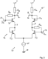
- the transimpedance amplifier 20 has two parallel current branches 7, 8 which extend between a supply voltage connection 9 and a ground connection 10.
- a current source 11 is provided on the ground connection side.
- a first current branch 7 has a first amplification transistor T1, which is designed as an npn transistor.
- the first amplification transistor T1 has a collector which is connected via the resistor R fp to the positive input terminal 32 of the transimpedance amplifier 20 and via a resistor R dp to the supply voltage.
- a base of the amplification transistor T1 is directly connected to the positive input terminal 32.
- a second amplification transistor T2, which is also designed as an npn transistor, is arranged in a second current branch 8.
- This amplification transistor T2 has a collector which is connected via the resistor R fn to the negative input terminal 34 of the transimpedance amplifier 20.
- a base of the amplification transistor T2 is also connected to the negative input terminal 34.
- the input current I in is the difference between the input currents I in+ and I in- .
- the output voltage U o is the difference between the voltages U vo+ and U vo- plus a constant offset voltage.
- the transimpedance amplifier 20 has an operating point adjustment part 12 in the first current branch 7 for adjusting the input and output voltages of the amplification transistor T1.
- the operating point voltage at the cathode 5 of the photodiode 2 is set by adjusting the operating point voltage at the input of the amplification transistor T1.
- a germanium photodiode is assumed, for which the desired operating point is a blocking voltage of approximately 1 V.
- the operating point adjustment part 12 has a transistor T3 which is connected in diode connection, i.e. short circuit of base and collector.
- a first transistor T3 is arranged in diode connection, with a collector of the transistor T3 being connected to an emitter of the amplification transistor T1. An emitter of the transistor T3 is connected to the current source 11.
- the transimpedance amplifier 20 has an operating point adjustment part 12' in the second current branch 8 for adjusting the input and output voltages of the amplifier transistor T2.
- the operating point voltage at the anode 3 of the photodiode 2 is set by adjusting the operating point voltage at the input of the amplifier transistor T2.
- the operating point adjustment part 12' has a transistor T4 in the second current branch 8, which is connected in diode connection, ie with a short circuit of base and collector.
- An emitter of transistor T4 is connected to the collector of the amplifier transistor T2 and the collector and base of the transistor T4 are connected to the supply connection 9 via a resistor R dn .
- the collector of the transistor T1 is connected to the supply terminal 9 via the resistor R dp .
- the transistors T3, T4 cause an offset of the differential input and output voltage, which depends on the desired operating point voltage of the photodiode 2.
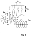
- the offset of the differential output voltage is in Figure 3 shown.
- a further embodiment of the invention for eliminating the offset of the differential output voltage U o is described in Figure 3 It comprises a transimpedance amplifier 20, which is symmetrically connected on the input side to a photodiode 2.
- An anode 3 of the photodiode 2 is connected to a negative input terminal 34 of the transimpedance amplifier 20 and a cathode 5 of the photodiode 2 is connected to a positive input terminal 32 of the transimpedance amplifier 20.
- the transimpedance amplifier 20 has a positive output terminal 35 or V o+ and a negative output terminal 33 or V o- , as can be seen from Figure 3 These two voltages are phase-shifted by 180° and have a different DC voltage component, resulting in an offset voltage U dif .
- U dif is constant or changes only slowly.
- a differential voltage compensation unit 13 according to Figure 3 by means of which the offset voltage or the DC voltage difference U dif between the positive Output terminal V o+ and the negative output terminal V o- of the transimpedance amplifier 20 is reduced to zero.
- This differential voltage compensation unit 13 is designed as a passive high-pass filter which has capacitances C which are respectively connected to the output terminals V o+ , V o- so that output signals U vo + ' and U vo- ' are produced at the modified output terminals V o+ ' and V o- ' which have the same DC voltage component compared to the voltages U vo+ , U vo- present at the output terminals V o+ , V o- .
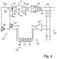
- a differential voltage compensation unit 13' can be provided, which is formed by a feedback circuit part 14.
- This feedback circuit part 14 has a differential low-pass filter 15, which is connected directly to the transimpedance amplifier 20 or to further amplifier stages 16 arranged on the output side of the transimpedance amplifier 20.
- the low-pass filter 15 is connected to an error correction amplifier 17.
- the error correction amplifier 17 is connected to an A/D converter 19, a register 22 and a D/A converter 18.
- a transistor circuit part 21 is provided, which consists of two transistors T5, T6.
- Collector terminals of the transistors T5, T6 are each connected to the negative input terminal 34 or positive input terminal 32 of the transimpedance amplifier 20.
- collector currents I osp , I osn of the transistors T5, T6 flow to the input terminals 34 and 32, respectively, and a current I ph through the photodiode 2.
- the feedback circuit part 14 results in a change in the DC component of the input current I in at the transimpedance amplifier 20 by means of an offset current that is set, which causes the output voltage signals U vo+ ' and U vo- ' to have the same DC voltage components.
- An advantage of using A/D converter 19, register 22 and D/A converter 18 is that the clock of the Register 22 can be switched on or off as required.
- the currents I osp and I osn are adjusted precisely and continuously. If, however, the clock is switched off, the last settings found for the currents I osp and I osn are retained and no longer change. This can be advantageous if, for example, the dynamic control behavior of the feedback circuit part 14 has an unfavorable effect on the output signal of the transimpedance amplifier 20. In this case, a fixed setting of the I osp and I osn may be necessary.
- the A/D converter 19, register 22 and the D/A converter 18 can be omitted and the outputs of the error correction amplifier 17 can be connected directly to the inputs of the transistors T5 and T6.
- transistors T1, T2, T3, T4, T5, T6 can also be designed as other types than bipolar transistors, for example field effect transistors.
- bipolar transistors are provided in the embodiments described here, it is clear to those skilled in the art that any of the bipolar transistors can be replaced in alternative embodiments by a variety of other types of transistors, such as field effect transistors.
- emitter, collector and base terminals of the bipolar transistors described here correspond to source, drain and gate terminals, respectively, in embodiments that include field effect transistors and can be used interchangeably when describing the embodiment. The use of the terms emitter, collector and base terminals does not therefore have a limiting effect on embodiments or the invention.
- pnp transistors can also be used instead of npn transistors.
- p-field effect transistors can be used instead of n-field effect transistors.
- the amplifiers formed by the amplification transistors T1 and T2 can also be replaced by multi-stage amplifier circuits. This can, for example, enable a higher bandwidth.
- the operating point adjustment parts 12 and 12' can also be implemented by V BE multipliers (see e.g. " VBE Multiplier", in Crecraft, David; Gergely, Stephen (May 21, 2002). Analog Electronics. Butterworth-Heinemann. p. 188. ISBN 0080475833 ) can be formed.
- V BE multipliers see e.g. " VBE Multiplier", in Crecraft, David; Gergely, Stephen (May 21, 2002). Analog Electronics. Butterworth-Heinemann. p. 188. ISBN 0080475833 ) can be formed.
- V BE multipliers compared to diodes is that they can generate voltages that are k*V BE , where k does not have to be an integer.
Landscapes
- Engineering & Computer Science (AREA)
- Power Engineering (AREA)
- Physics & Mathematics (AREA)
- General Physics & Mathematics (AREA)
- Spectroscopy & Molecular Physics (AREA)
- Nonlinear Science (AREA)
- Amplifiers (AREA)
Description
- Die Erfindung betrifft eine Schaltung enthaltend einen Transimpedanzverstärker zur Umsetzung zweier Eingangsströme in zwei Ausgangsspannungen mit einem ersten Verstärkerteil enthaltend einen ersten Eingang, an dem eine erste Eingangsspannung anliegt und in den ein erster Eingangsstrom fließt, und mit einem zweiten Verstärkerteil enthaltend einen zweiten Eingang, an dem eine zweite Eingangsspannung anliegt und in den ein zweiter Eingangsstrom fließt.
- Transimpedanzverstärker werden insbesondere dazu eingesetzt, um ein Eingangsstromsignal in ein Ausgangsspannungssignal umzuwandeln. Das Eingangsstromsignal kann beispielsweise der Strom einer Fotodiode sein. Der Transimpedanzverstärker empfängt das aus der Fotodiode ausgegebene Stromsignal, wandelt das Stromsignal in ein entsprechendes Spannungssignal um und gibt das Spannungssignal aus. Das Spannungssignal kann gegebenenfalls durch einen Verstärker verstärkt werden.
- Aus der
US 5 345 073 A ist eine Schaltung mit einem Transimpedanzverstärker bekannt, an dessen Eingang eine Fotodiode symmetrisch angeschlossen ist. Hierbei sind eine Kathode und eine Anode der Fotodiode direkt mit dem Eingang des Transimpedanzverstärkers verbunden. Der Transimpedanzverstärker umfasst zwei parallele Stromzweige, in denen jeweils eine Anzahl von Transistoren zur Verstärkung angeordnet ist. Vorteilhaft an der Schaltung ist, dass die Fotodiode direkt, d.h. ohne Koppelkondensatoren an den Verstärkereingang angeschlossen ist, weil dadurch keine zusätzlichen Bauelemente im Signalpfad liegen, wodurch das Hochfrequenzverhalten und Rauschen verbessert, sowie Kosten reduziert werden. Die Fotodiode ist symmetrisch angeschlossen, wodurch zum einen der Differenzbetrieb der Fotodiode ermöglicht und somit zum einen die Gleichtaktunterdrückung verbessert wird und zum anderen sowohl der Strom der Anode als auch der Strom der Kathode der Diode als Eingangsströme des Verstärkers genutzt werden können. Die Fotodiode kann mit geeigneten Arbeitspunktspannungen vorgespannt werden. Nachteilig an der bekannten Schaltung des Transimpedanzverstärkers ist, dass an seinem Eingang zusätzliche Verstärker (Transistoren und Stromquellentransistoren) benötigt werden, was die Schaltung komplexer macht und das Rauschverhalten verschlechtert. Ein weiterer Nachteil ist, dass der zusätzliche Verstärker am Eingang eine Erhöhung der Versorgungsspannung um mindestens zwei Kollektor-Emitter-Spannungen (nämlich Kollektor-Emitter-Spannung eines Stromquellentransistors und Kollektor-Emitter-Spannung eines Transistors in Basisschaltung) zuzüglich der Arbeitspunktspannung der Diode erforderlich macht. - Die Druckschrift "Transimpedance amplifier with differential photodiode current sensing" (Zand B; Phang K; Johns D A, Proceedings of the 1999 IEEE International Symposium on Circuits and Systems / ISCAS '99, May 30 - June 2, 1999, Orlando, Florida, IEEE Service Center, Piscataway, NJ, Vol:2, Page(s):11-624 - 11-627) offenbart einen Transimpedanzverstärker mit zwei Verstärkerteilen, die an eine gemeinsame Versorgungsspannung angeschlossen sind.
- Die europäische Offenlegungsschrift
EP 0 556 000 A1 offenbart einen Differenzverstärker für ein optisches Speichersystem mit einem Fotodiodendetektor, wobei der Differenzverstärker Eingänge zum Empfangen eines Differenzeingangsstroms von der Fotodiode und Ausgänge zum Bereitstellen eines entsprechenden Differenzausgangsspannungssignals aufweist. Der Differenzverstärker ist gekennzeichnet durch eine Vorwärts-Transimpedanzverstärkung und eine Diodenvorspannungsstufe, die die Eingänge und die Ausgänge verbindet. - Aufgabe der vorliegenden Erfindung ist es, eine Schaltung mit einem Transimpedanzverstärker, an dem eingangsseitig symmetrisch eine Fotodiode ohne Koppelkondensatoren angeschlossen ist und die es ermöglicht eine Arbeitspunktspannung der Fotodiode einzustellen, derart weiterzubilden, dass das Rauschen, die Versorgungsspannung und die Schaltungskomplexität verringert werden.
- Zur Lösung dieser Aufgabe sind die Merkmale des Patentanspruchs 1 vorgesehen..
- Nach der Erfindung ist ein Transimpedanzverstärker vorgesehen, der über ein vergleichsweise geringeres Rauschverhalten, eine niedrige Versorgungsspannung und eine geringere Schaltungskomplexität verfügt. Er kann vielseitig eingesetzt werden, insbesondere zur rauscharmen Verstärkung von Stromsignalen von Detektoren oder Sensoren im Hochfrequenzbereich, z.B. Fotodetektoren, Hall-Sensoren, Drucksensoren oder Temperatursensoren.
- Nach einer bevorzugten Ausführungsform der Erfindung ist an einen Transimpedanzverstärker eingangsseitig symmetrisch eine Fotodiode angeschlossen, wobei Anode und Kathode der Fotodiode direkt an Eingangsanschlüssen des Transimpedanzverstärkers angeschlossen sind. Am Eingang des Transimpedanzverstärkers sind keine zusätzlichen Bauelemente, wie Kondensatoren und Widerstände, erforderlich, die die Bandbreite und die Empfindlichkeit bzw. das Rauschen des Transimpedanzverstärkers verschlechtern würden. Die Erfindung ermöglicht auf kosteneffiziente Weise die Bereitstellung eines Transimpedanzverstärkers. Der Transimpedanzverstärker enthält ein Arbeitspunktanpassungsteil, mittels dessen eine Anpassung z.B. an eine Sperrspannung der Fotodiode ermöglicht wird. Vorteilhaft können hierdurch einfach unterschiedliche Fotodiodentypen am Eingang des Transimpedanzverstärkers angeschlossen werden bzw. der Arbeitspunkt der Fotodiode so eingestellt werden, dass der Dunkelstrom minimiert oder die Bandbreite maximiert werden. Da eingangsseitig des Transimpedanzverstärkers keine zusätzlichen Bauelemente angeordnet sind, kann das Rauschen des Transimpedanzverstärkers gering und die Bandbreite hoch gehalten werden.
- Nach einer Weiterbildung der Erfindung ist ausgangsseitig des Transimpedanzverstärkers eine Differenz-Spannungsausgleichseinheit vorgesehen, mittels dessen eine Gleichspannungsdifferenz zwischen einem positiven Ausgangsanschluss und einem negativen Ausgangsanschluss des Transimpedanzverstärkers auf Null reduziert werden kann.
- Nach einer bevorzugten Ausführungsform der Erfindung ist die Differenz-Spannungsausgleichseinheit durch einen passiven Hochpassfilter gebildet. Dieser besteht aus Kapazitäten, die mit den Ausgangsanschlüssen verbunden sind. Vorteilhaft können hierdurch die Spannungssignalverläufe an dem positiven Ausgangsanschluss und an dem negativen Ausgangsanschluss auf ein gemeinsames Gleichspannungsniveau gesetzt werden.
- Nach einer Weiterbildung der Erfindung ist die Differenz-Spannungsausgleichseinheit durch ein Rückkopplungsschaltungs-Teil gebildet. Dieses umfasst einen Tiefpassfilter, einen Fehlerkorrekturverstärker und ein Transistorschaltungs-Teil, so dass eingangsseitig des Transimpedanzverstärkers ein Differenzstrom fließt, der sich automatisch so einstellt, dass die Spannungssignalverläufe an dem positiven Ausgangsanschluss und an dem negativen Ausgangsanschluss auf ein gemeinsames Gleichspannungsniveau gesetzt werden . Im Vergleich zu der vorgenannten Weiterbildung kann hierdurch zusätzlich ein RSSI (Received Signal Strength Indicator), Burst Mode Operationen und Kanalausfallüberwachung implementiert werden.
- Die Erfindung ermöglicht insbesondere einen geringen Versorgungsspannungsdurchgriff (hohe Power Supply Rejection Ratio, PSRR), eine geringe Gleichtaktverstärkung (common-mode gain) bei gleichzeitig hoher Differenzverstärkung (differential-mode gain) aufgrund der volldifferenziellen Eingangspegelstandes und des volldifferenziellen Aufbaus des Transimpedanzverstärkers. Zusätzliche parasitäre Kapazitäten sind nicht vorhanden, da am Eingang des Transimpedanzverstärkers die Fotodiode direkt an den Eingangsanschlüssen angeschlossen ist. Die Erfindung kann vorzugsweise in monolithischen Mehrkanalempfängern eingesetzt werden, z.B. auf Basis von Siliziumphotonik-Technologien.
- Ausführungsbeispiele der Erfindung werden nachfolgend anhand der Zeichnungen näher erläutert.
- Es zeigen:
- Fig. 1
- ein Blockschaltbild der Erfindung
- Fig. 2
- eine beispielhafte detaillierte Ausführungsform der Erfindung
- Fig. 3
- eine alternative Ausführungsform der erfindungsgemäßen Schaltung mit Differenzspannungsausgleichseinheit ohne Rückkopplung
- Fig. 4
- eine alternative Ausführungsform der erfindungsgemäßen Schaltung mit Differenzspannungsausgleichseinheit mit Rückkopplung
- Die erfindungsgemäße Schaltung gemäß
Figur 1 umfasst einen Transimpedanzverstärker 20, der über ein erstes Verstärkerteil 30 und ein zweites Verstärkerteil 31 verfügt. Das erste Verstärkerteil 30 und das zweite Verstärkerteil 31 sind an eine gemeinsame Versorgungsspannung 9 angeschlossen. Zur Einstellung eines Arbeitspunktes sind der erste Verstärkerteil 30 und der zweite Verstärkerteil 31 jeweils an dieselbe bzw. gemeinsame Stromquelle 11 angeschlossen. Die Schaltung 20 ist als ein Transimpedanzverstärker ausgebildet. - Der erste Verstärkerteil 30 weist einen ersten Eingangsanschluss 32 auf, an dem eine erste Eingangsspannung Uin+ anliegt und in den ein erster Eingangsstrom Iin+ fließt. Ferner weist der erste Verstärkerteil 30 einen ersten Ausgangsanschluss 33 auf, an dem die Ausgangsspannung Uvo- anliegt.
- Der zweite Verstärkerteil 31 weist einen zweiten Eingangsanschluss 34 auf, an dem eine zweite Eingangsspannung Uin- anliegt und in den ein zweiter Eingangsstrom Iin- fließt. Ferner weist der zweite Verstärkerteil 31 einen zweiten Ausgangsanschluss 35 auf, an dem die zweite Ausgangsspannung Uvo+ anliegt.
- Nach einer nicht dargestellten alternativen Ausführungsform der Schaltung 20 kann die Stromquelle 11 entfallen, so dass der erste Verstärkerteil 30 und der zweite Verstärkerteil 31 jeweils an einem Masseanschluss angeschlossen sind. Der Entfall der Stromquelle 11 ist für solche Einsatzfälle vorteilhaft, in denen die Schaltung mit einer relativ geringen Versorgungsspannung betrieben wird. Nachteilig ist der höhere Versorgungsspannungsdurchgriff (niedrigere Power Supply Rejection Ratio, PSRR).
- Der erste Verstärkerteil 30 und der zweite Verstärkerteil 31 können jeweils als einstufige oder mehrstufige Transistoranordnung ausgebildet sein. Vorzugsweise weisen sie die gleichen Transistoren bzw. Anzahl von Transistoren auf. Der erste Verstärkerteil 30 und der zweite Verstärkerteil 31 sind jeweils so ausgebildet, dass die erste Ausgangsspannung Uvo- proportional zu dem ersten Eingangsstrom Iin+ und die zweite Ausgangsspannung Uvo+ proportional zu dem zweiten Eingangsstrom Iin- ist. Vorteilhaft wird hierdurch ein Transimpedanzverstärker bereitgestellt, der im Vergleich zu dem in der
US 5 345 073 A beschriebenen Transimpedanzverstärker ein wesentlich geringeres Rauschen und eine kleinere Versorgungsspannung aufweist. Die Schaltung 20 kann auch als reiner Spannungsverstärker ohne angeschlossenen Sensor genutzt werden. Alternativ kann an den Eingängen 32, 34 des ersten Verstärkerteils 30 und des zweiten Verstärkerteils 31 ein Sensor oder ein Detektor, beispielsweise ein Hallsensor oder eine Fotodiode, angeschlossen werden. InFigur 1 ist beispielhaft die Fotodiode 2 zwischen dem ersten Eingangsanschluss 32 des ersten Verstärkerteils 30 und dem zweiten Eingangsanschluss 34 des zweiten Verstärkerteils 31 angeschlossen. - Der Sensor 2 ist mit einem ersten Anschluss direkt an den Eingang 32 des ersten Verstärkerteils 30 und mit einem zweiten Anschluss an den Eingang 34 des zweiten Verstärkerteils 31 angeschlossen. Vorzugsweise wird der Sensor 2 mit symmetrischen elektrischen Eigenschaften eingesetzt, um ein bestes Ergebnis des Transimpedanzverstärkers zu erzielen. Hierzu weisen die Eingangsanschlüsse 32, 34 der Verstärkerteile 30, 31 gleiche Eigenschaften und Ladebedingungen auf. Alternativ funktioniert die Schaltung 20 auch mit asymmetrischen elektrischen Eigenschaften.
- In einer weiteren Ausgestaltung der Erfindung kann der Sensors 2 nur an einen Eingang, d.h. nur an Eingang 32 des ersten Verstärkerteils 30 oder den Eingang 34 des zweiten Verstärkerteils 31 angeschlossen werden. Der jeweils andere Eingang bleibt dann z.B. unbeschaltet. In diesem Fall wird der Sensor nicht symmetrisch betrieben, und der Transimpedanzverstärker 20 liefert ein differentielles Ausgangssignal, das proportional zum Sensorstrom ist. Weiterhin können auch zwei Sensoren 2 an die Eingänge 32, 34 derart angeschlossen werden, so dass der eine Sensor 2 an den Eingang 32 des ersten Verstärkerteils 30 und der andere Sensor 2 an den Eingang 34 des zweiten Verstärkerteils 31 angeschlossen wird. Der Transimpedanzverstärker 20 gibt dann eine differentielle Spannung aus, die proportional zur Differenz der Sensorströme ist.
- Eine mögliche detaillierte Ausgestaltung des Transimpedanzverstärkers 20 ist in
Figur 2 dargestellt. Der Transimpedanzverstärker 20 weist zwei parallele Stromzweige 7, 8 auf, die sich zwischen einem Versorgungsspannungsanschluss 9 und einem Masseanschluss 10 erstrecken. Massenanschlussseitig ist eine Stromquelle 11 vorgesehen. - Ein erster Stromzweig 7 weist einen ersten Verstärkungstransistor T1 auf, der als ein npn-Transistor ausgebildet ist. Der erste Verstärkungstransistor T1 weist einen Kollektor auf, der über den Widerstand Rfp mit dem positiven Eingangsanschluss 32 des Transimpedanzverstärkers 20 und über einen Widerstand Rdp mit der Versorgungsspannung verbunden ist. Eine Basis des Verstärkungstransistors T1 ist direkt mit dem positiven Eingangsanschluss 32 verbunden. In einem zweiten Stromzweig 8 ist ein zweiter Verstärkungstransistor T2 angeordnet, der ebenfalls als npn-Transistor ausgebildet ist. Dieser Verstärkungstransistor T2 weist einen Kollektor auf, der über den Widerstand Rfn mit dem negativen Eingangsanschluss 34 des Transimpedanzverstärkers 20 verbunden ist. Eine Basis des Verstärkungstransistors T2 ist ebenfalls mit dem negativen Eingangsanschluss 34 verbunden. Die Verstärkungstransistoren T1 und T2 bilden einen Differenzverstärker. Wenn die Widerstände Rfn und Rfp , sowie die Widerstände Rdp und Rdn paarweise gleich sind, stellt der Wert Rfn = Rfp = Rf näherungsweise die Verstärkung bzw. Transimpedanz Z dar, um die ein Eingangsstrom Iin verstärkt wird zu einer Ausgangsspannung Uo. Der Eingangsstrom Iin ergibt sich als Differenz aus dem Eingangsstrom Iin+ und Iin-. Die Ausgangsspannung Uo ergibt sich aus der Differenz der Spannung Uvo+ und Uvo- zuzüglich einer konstanten Offsetspannung.
- Zusätzlich weist der Transimpedanzverstärker 20 im ersten Stromzweig 7 ein Arbeitspunktanpassungsteil 12 zur Anpassung der Eingangs- und Ausgangsspannungen von Verstärkungstransistor T1 auf. Gleichzeitig wird durch Anpassung der Arbeitspunktspannung am Eingang von Verstärkungstransistor T1 die Arbeitspunktspannung an der Kathode 5 der Fotodiode 2 eingestellt. Im vorliegenden Ausführungsbeispiel wird eine Germaniumfotodiode angenommen, bei der der gewünschte Arbeitspunkt eine Sperrspannung von ca. 1 V ist. Das Arbeitspunktanpassungsteil 12 weist zu diesem Zweck einen Transistoren T3 auf, der in Diodenverbindung, d.h. Kurzschluss von Basis und Kollektor geschaltet ist. In dem ersten Stromzweig 7 ist ein erster Transistor T3 in Diodenverbindung angeordnet, wobei ein Kollektor des Transistors T3 mit einem Emitter des Verstärkungstransistors T1 verbunden ist. Ein Emitter des Transistors T3 ist mit der Stromquelle 11 verbunden.
- Des Weiteren weist der Transimpedanzverstärker 20 im zweiten Stromzweig 8 ein Arbeitspunktanpassungsteil 12' zur Anpassung der Eingangs- und Ausgangsspannungen von Verstärkertransistor T2 auf. Gleichzeitig wird durch Anpassung der Arbeitspunktspannung am Eingang von Verstärkungstransistor T2 die Arbeitspunktspannung an der Anode 3 der Fotodiode 2 eingestellt. Das Arbeitspunktanpassungsteil 12' weist zu diesem Zweck einen Transistor T4 im zweiten Stromzweig 8 auf, der in Diodenverbindung, d.h. mit Kurzschluss von Basis und Kollektor geschaltet ist. Dabei wird ein Emitter von Transistor T4 mit dem Kollektor des Verstärkungstransistors T2 und Kollektor und Basis des Transistors T4 über einen Widerstand Rdn mit dem Versorgungsanschluss 9 verbunden.
- Der Kollektor des Transistors T1 ist über den Widerstand Rdp mit dem Versorgungsanschluss 9 verbunden. Die Transistoren T1, T2 ermöglichen die Verstärkung des eingangsseitigen Differenzsignals Iin = Iin+ - Iin- zu einer Ausgangsspannung Uo mit der Verstärkung Rf, wobei zusätzlich eine konstante Offsetspannung in Uo enthalten ist. Die Transistoren T3, T4 bewirken einen Offset der differentiellen Eingangs- und Ausgangsspannung, der von der gewünschten Arbeitspunktspannung der Fotodiode 2 abhängig ist.
- Der Offset der differentiellen Ausgangsspannung ist in
Figur 3 dargestellt. An den Ausgangsklemmen Vo+ bzw. Vo- 35,33 der inFigur 3 dargestellten Schaltung liegen die Spannungen Uvo+ bzw. Uvo- an, die einen unterschiedlichen Gleichanteil aufweisen und betragsmäßig gleiche Wechselanteile aufweisen, so dass die differentiellen Ausgangsspannung Uo = Uvo+ - Uvo- eine konstante Offsetspannung aufweist. - Eine weitere Ausgestaltung der Erfindung zur Eliminierung des Offsets der differentiellen Ausgangsspannung Uo ist in
Figur 3 gezeigt. Sie umfasst einen Transimpedanzverstärker 20, der eingangsseitig symmetrisch an eine Fotodiode 2 angeschlossen ist. Eine Anode 3 der Fotodiode 2 ist an einem negativen Eingangsanschluss 34 des Transimpedanzverstärkers 20 und eine Kathode 5 der Fotodiode 2 mit einem positiven Eingangsanschluss 32 des Transimpedanzverstärkers 20 verbunden. Der Transimpedanzverstärker 20 weist einen positiven Ausgangsanschluss 35 bzw. Vo+ und einen negativen Ausgangsanschluss 33 bzw. Vo- auf, wie ausFigur 3 ersichtlich ist. Diese beiden Spannungen sind um 180° phasenverschoben und weisen einen unterschiedlichen Gleichspannungsanteil auf, so dass sich eine Offset-Spannung Udif ergibt. Typischerweise ist Udif konstant oder ändert sich nur langsam. Um die Offset-Spannung Udif auf null zu reduzieren, ist eine Differenz-Spannungsausgleichseinheit 13 gemäßFigur 3 vorgesehen, mittels derer die Offset-Spannung bzw. die Gleichspannungsdifferenz Udif zwischen dem positiven Ausgangsanschluss Vo+ und dem negativen Ausgangsanschluss Vo- des Transimpedanzverstärkers 20 auf Null reduziert wird. Diese Differenz-Spannungsausgleicheinheit 13 ist als ein passives Hochpassfilter ausgebildet, das Kapazitäten C aufweist, die jeweils an den Ausgangsanschlüssen Vo+, Vo-angeschlossen sind, so dass sich an den modifizierten Ausgangsanschlüssen Vo+' und Vo-' Ausgangssignale Uvo+' und Uvo-' ergeben, die im Vergleich zu den an den Ausgangsanschlüssen Vo+, Vo- anliegenden Spannungen Uvo+, Uvo- den gleichen Gleichspannungsanteil aufweisen. - Nach einer alternativen Ausführungsform gemäß
Figur 4 kann eine Differenzspannungsausgleichseinheit 13' vorgesehen sein, die durch ein Rücckopplungsschaltungs-Teil 14 gebildet ist. Dieses Rückkopplungsschaltungs-Teil 14 weist einen differentiellen Tiefpassfilter 15 auf, der direkt an dem Transimpedanzverstärker 20 oder an ausgangsseitig des Transimpedanzverstärkers 20 angeordneten weiteren Verstärkerstufen 16 angeschlossen ist. Im Rückkopplungszweig schließt sich an den Tiefpassfilter 15 ein Fehlerkorrekturverstärker 17 an. An den Fehlerkorrekturverstärker 17 schließt sich ein A/D-Wandler 19, ein Register 22, sowie ein D/A-Wandler 18 an. Ausgangsseitig des D/A-Wandlers 19 ist ein Transistorschaltungs-Teil 21 vorgesehen, das aus zwei Transistoren T5, T6 besteht. - Kollektoranschlüsse der Transistoren T5, T6 sind jeweils an den negativen Eingangsanschluss 34 bzw. positiven Eingangsanschluss 32 des Transimpedanzverstärkers 20 angeschlossen. Im Betriebszustand fließen Kollektorströme Iosp, Iosn der Transistoren T5, T6 zu den Eingangsanschlüssen 34 bzw. 32 und ein Strom Iph durch die Fotodiode 2.. Durch das Rückkopplungsschaltungs-Teil 14 ergibt sich mittels eines sich einstellenden Offsetstroms eine Änderung des Gleichanteils des Eingangsstrom Iin an dem Transimpendanzverstärker 20, der bewirkt, dass die Ausgangspannungssignale Uvo+' und Uvo-' die gleichen Gleichspannungsanteile aufweisen. Ein Vorteil der Verwendung von A/D-Wandler 19, Register 22 und D/A-Wandler 18 ist, dass der Takt des Registers 22 je nach Bedarf ein- oder ausgeschaltet werden kann. Wird der Takt eingeschaltet, werden die Ströme Iosp und Iosn genau und kontinuierlich nachgestellt. Wird der Takt dagegen ausgeschaltet, werden die zuletzt gefundenen Einstellungen für die Ströme Iosp und Iosn beibehalten und ändern sich nicht mehr. Dies kann vorteilhaft sein, wenn z.B. das dynamische Regelverhalten des Rückkopplungsschaltungsteils 14 das Ausgangssignal des Transimpedanzverstärkers 20 ungünstig beeinflusst. In diesem Fall kann eine feste Einstellung der Iosp und Iosn erforderlich sein.
- Nach einer alternativen nicht dargestellten Ausführungsform der Erfindung können der A/D-Wandler 19, Register 22 und der D/A-Wandler 18 weggelassen werden und die Ausgänge des Fehlerkorrekturverstärkers 17 direkt mit den Eingängen der Transistoren T5 und T6 verbunden werden.
- Es versteht sich, dass die genannten Transistoren T1, T2, T3, T4, T5, T6 auch andere Arten als Bipolartransistoren, beispielsweise Feldeffekttransistoren, ausgebildet sein können. Obwohl in den hierin beschriebenen Ausführungsformen die Bipolartransistoren vorgesehen sind, leuchtet es dem Fachmann ein, dass beliebige der Bipolartransistoren in alternativen Ausführungsformen durch eine Vielfalt anderer Arten von Transistoren, wie zum Beispiel Feldeffekttransistoren, ersetzt werden können. In dieser Hinsicht entsprechen Emitter-, Kollektor- und Basisanschlüsse der hier beschriebenen Bipolartransistoren in Ausführungsformen, die Feldeffekttransistoren umfassen, Source-, Drain- bzw. Gate-Anschlüsse und können beim Beschreiben der Ausführungsform austauschbar verwendet werden. Die Verwendung der Begriffe Emitter-, Kollektor- und Basisanschlüsse wirkt sich demgemäß nicht begrenzend auf Ausführungsformen bzw. der Erfindung aus. Desgleichen leuchtet es dem Fachmann ein, dass, bei geeigneter Einstellung der Arbeitspunktspannungen und -ströme der Transistoren auch pnp-Transistoren, statt npn-Transistoren, bzw. statt n-Feldeffekttranistoren auch p-Feldeffekttransistoren verwendet werden können.
- Die hierin abgebildeten Blockschaltbilder sind nur ein Beispiel. Viele Abwandlungen dieser Blockschaltbilder oder der hierin beschriebenen Operationen sind möglich, ohne vom Geist der Erfindung abzuweichen. Zum Beispiel können die Schaltungen in einer anderen Reihenfolge angeordnet sein oder können Schaltungen hinzugefügt, gelöscht oder geändert werden. Alle diese Abwandlungen werden als Bestandteil der beanspruchten Erfindung angesehen.
- In einer weiteren Ausführungsform können die durch die Verstärkungstransistoren T1 und T2 gebildeten Verstärker auch jeweils durch mehrstufige Verstärkerschaltungen ersetzt werden. Dies kann z.B. eine höhere Bandbreite ermöglichen.
- In einer weiteren Ausführungsform können die Arbeitspunktanpassungsteile 12 und 12' auch durch VBE-Multiplizierer (siehe z.B. "VBE-Multiplier", in Crecraft, David; Gergely, Stephen (May 21, 2002). Analog Electronics. Butterworth-Heinemann. p. 188. ISBN 0080475833) gebildet werden. Vorteilhaft ist beim VBE-Multiplizierern im Vergleich zu Dioden, dass damit Spannungen erzeugt werden können die k*VBE betragen, wobei k nicht ganzzahlig sein muss.
Claims (14)
- Schaltung enthaltend einen Transimpedanzverstärker (20) zur Umsetzung zweier Eingangsströme (Iin+, Iin-) in zwei Ausgangsspannungen (Uvo-, Uvo+) mit einem ersten Stromzweig (7) enthaltend einen ersten Eingang (32), an dem eine erste Eingangsspannung (Uin+) anliegt und in den ein erster Eingangsstrom (Iin+) fließt, und mit einem zweiten Stromzweig (8) enthaltend einen zweiten Eingang (34), an dem eine zweite Eingangsspannung (Uin) anliegt und in den ein zweiter Eingangsstrom (Iin-) fließt, wobei der erste Stromzweig (7) und der zweite Stromzweig (8) an eine gemeinsame Versorgungsspannung (9) an einem Versorgungsanschluss angeschlossen sind,wobei der erste Stromzweig (7) und der zweite Stromzweig (8) an eine gemeinsame Stromquelle (11) angeschlossen sind,wobei der erste Eingang (32) und der zweite Eingang (34) eine unterschiedliche Gleichspannung aufweisenwobei der erste Stromzweig (7) und der zweite Stromzweig (8) derart ausgebildet sind, dass eine Ausgangsspannung (Uvo-) des ersten Stromzweigs (7) proportional zu dem ersten Eingangsstrom (Iin+) des ersten Stromzweigs (7) und eine Ausgangsspannung (Uvo+) des zweiten Stromzweigs (8) proportional zu dem zweiten Eingangsstrom (Iin-) des zweiten Stromzweigs (8) ist,wobei ein Sensor (2) direkt mit dem ersten und zweiten Eingang (32, 34) verbunden ist,wobei die zwei parallelen Stromzweige (7, 8) jeweils eine Anzahl von Transistoren (T1, T2, T3, T4) aufweisen,wobei sich die Stromzweige (7, 8) zwischen dem Versorgungsanschluss und einem ersten Anschluss der Stromquelle (11) erstrecken, wobei ein zweiter Anschluss der Stromquelle mit der Masse verbunden ist,wobei ein erster Anschluss (3) des Sensors (2) mit einem Basisanschluss eines in dem ersten Stromzweig (7) angeordneten ersten Verstärkungstransistors (T1) und über einen ersten Widerstand (Rfp) mit einem Kollektoranschluss des ersten Verstärkungstransistors (T1) verbunden ist,wobei der Kollektor des ersten Verstärkungstransistors (T1) über einen dritten Widerstand (Rdp ) mit der Versorgungsspannung verbunden ist,wobei ein zweiter Anschluss (5) des Sensors (2) mit einem Basisanschluss eines in dem zweiten Stromzweig (8) angeordneten zweiten Verstärkungstransistors (T2) und über einen zweiten Widerstand (Rfn) mit einem Kollektoranschluss des zweiten Verstärkertransistors (T2) verbunden ist,wobei im ersten Stromzweig (7) ein erstes Arbeitspunktanpassungsteil (12) zur Anpassung der Eingangs- und Ausgangsspannungen des ersten Verstärkungstransistors (T1) vorgesehen ist, das zwischen dem Emitter des ersten Verstärkungstransistors (T1) und dem ersten Anschluss der Stromquelle (11) angeordnet ist, wobei durch die Anpassung der Arbeitspunktspannung am Eingang des ersten Verstärkungstransistors (T1) gleichzeitig die Arbeitspunktspannung am zweiten Anschluss (5) des Sensors (2) eingestellt wird,wobei im zweiten Stromzweig (8) ein zweites Arbeitspunktanpassungsteil (12') zur Anpassung der Eingangs- und Ausgangsspannungen des zweiten Verstärkertransistors (T2) vorgesehen ist, das zwischen dem Kollektor des zweiten Verstärkungstransistors (T2) und einem ersten Anschluss eines vierten Widerstandes (Rdn ) angeschlossen ist, der an seinem zweiten Anschluss mit der Versorgungsspannung (9) verbunden ist, wobei durch die Anpassung der Arbeitspunktspannung am Eingang des zweiten Verstärkungstransistors (T2) gleichzeitig die Arbeitspunktspannung am ersten Anschluss (3) des Sensors (2) eingestellt wird, undwobei der erste Widerstand (Rfp) und der zweite Widerstand (Rfn) gleich sind einerseits und wobei der dritte Widerstand (Rdp) und der vierte Widerstand (Rdn) gleich sind andererseits undwobei der erste und der zweite Verstärkungstransistor (T1 und T2) einen Differenzverstärker bilden.
- Schaltung nach Anspruch 1, dadurch gekennzeichnet, dass die Stromquelle (11) durch einen Kurzschluss ersetzt wird.
- Schaltung nach einem der Ansprüche 1 bis 2, dadurch gekennzeichnet, dass der erste Stromzweig (7) und der zweite Stromzweig (8) als eine einstufige oder mehrstufige Transistoranordnung ausgebildet sind.
- Schaltung nach einem der Ansprüche 1 bis 3, dadurch gekennzeichnet, dass ein Sensor (2), insbesondere eine Fotodiode, mit einem ersten Anschluss direkt an dem ersten Eingang (32) des ersten Stromzweigs (7) und mit einem zweiten Anschluss direkt an dem zweiten Eingang (34) des zweiten Stromzweigs (8) angeschlossen ist.
- Schaltung nach einem der Ansprüche 1 bis 4, dadurch gekennzeichnet, dass der erste Stromzweig (7) und der zweite Stromzweig (8) die gleichen Transistoren und/oder die gleiche Anzahl von Transistoren aufweisen.
- Schaltung nach einem der Ansprüche 1 bis 5, dadurch gekennzeichnet, dass das erste Arbeitspunktanpassungsteil (12) einen Transistor (T3) mit Kurzschluss zwischen der Basis und dem Kollektor desselben aufweist und dass das zweite Arbeitspunktanpassungsteil (12') ebenfalls einen Transistor (T4) mit Kurzschluss zwischen der Basis und dem Kollektor desselben aufweist.
- Schaltung nach einem der Ansprüche 1 bis 6, dadurch gekennzeichnet, dass eine Anzahl von Transistoren (T5) des ersten Arbeitspunktanpassungsteils (12) in Abhängigkeit von einer Arbeitspunktspannung des Sensors (2) vorgesehen ist.
- Schaltung nach einem der Ansprüche 1 bis 7, dadurch gekennzeichnet, dass eine Anzahl von Transistoren (T6) des zweiten Arbeitspunktanpassungsteils (12') zum symmetrischen Betrieb der Gesamtschaltung vorgesehen ist.
- Schaltung nach einem der Ansprüche 1 bis 8, dadurch gekennzeichnet, dass ein positiver Ausgangsanschluss (35, Vo+) des Transimpedanzverstärkers (20) mit einem Kollektoranschluss des zweiten Arbeitspunktanpassungsteils (12', T4) und ein negativer Ausgangsanschluss (33, Vo-) des Transimpedanzverstärkers (20) mit einem Kollektoranschluss des ersten Verstärkungstransistors (T1) verbunden ist.
- Schaltung nach einem der Ansprüche 1 bis 9, dadurch gekennzeichnet, dass an Ausgangsanschlüssen (35, 33; Vo+, Vo-) des Transimpedanzverstärkers (20) eine Anzahl von Verstärkerstufen (16) angeschlossen ist mit einem positiven Ausgangsanschluss (Vo+') und mit einem negativen Ausgangsanschluss (Vo-').
- Schaltung nach einem der Ansprüche 1 bis 10, dadurch gekennzeichnet, dass an den Ausgangsanschlüssen (35, 33 ; Vo+, Vo-) des Transimpedanzverstärkers (20) oder der Verstärkerstufen (16) eine Differenz-Spannungsausgleichseinheit (13, 13') vorgesehen ist, mittels derer eine Gleichspannungsdifferenz (Udif) zwischen der Spannung (Uvo+) am positiven Ausgangsanschluss (35, Vo+) und einer Spannung (Uvo-) am negativen Ausgangsanschluss (Vo-, 33) des Transimpedanzverstärkers (20) auf Null reduziert wird.
- Schaltung nach Anspruch 11, dadurch gekennzeichnet, dass die Differenz-Spannungsausgleichseinheit (13) durch ein differentielles, passives Hochpassfilter gebildet ist, das durch jeweils an den Ausgangsanschlüssen (33, 35; Vo+, Vo-) des Transimpedanzverstärkers (20) angeschlossene Kapazitäten (C) gebildet ist.
- Schaltung nach Anspruch 11, dadurch gekennzeichnet, dass die Differenz-Spannungsausgleichseinheit (13') durch ein Rücckopplungsschaltungs-Teil (14) gebildet ist, das mehrere in Reihe geschaltete Komponenten umfasst:- einen differentiellen Tiefpassfilter (15), der mit den Ausgangsanschlüssen (33, 35; Vo+, Vo-) des Transimpedanzverstärkers (20) oder der Verstärkerstufen (16, Vo+', Vo-') verbunden ist,- einen Fehlerkorrekturverstärker (17),- ein Transistorschaltungs-Teil (21), das mit einem ersten Anschluss (3) und einem zweiten Anschluss (5) eines Sensors (2) derart verbunden ist, dass eine am Ausgang (33, 35) des Transimpedanzverstärkers (20) anliegende differentielle Gleichspannung zu Null wird.
- Schaltung nach Anspruch 13, dadurch gekennzeichnet, dass das Rückkopplungsschaltungs-Teil (14) zwischen Fehlerkorrekturverstärker (17) und Transistorschaltungsteil (21) eine Reihenschaltung aus A/D-Wandler (19), Register (22) und D/A-Wandler (18) aufweist.
Applications Claiming Priority (2)
| Application Number | Priority Date | Filing Date | Title |
|---|---|---|---|
| DE102017111197.2A DE102017111197A1 (de) | 2017-05-23 | 2017-05-23 | Transimpedanzverstärker-Schaltung |
| PCT/DE2018/200048 WO2018215030A1 (de) | 2017-05-23 | 2018-05-15 | Transimpedanzverstärker-schaltung |
Publications (2)
| Publication Number | Publication Date |
|---|---|
| EP3631978A1 EP3631978A1 (de) | 2020-04-08 |
| EP3631978B1 true EP3631978B1 (de) | 2024-07-31 |
Family
ID=62684566
Family Applications (1)
| Application Number | Title | Priority Date | Filing Date |
|---|---|---|---|
| EP18732649.1A Active EP3631978B1 (de) | 2017-05-23 | 2018-05-15 | Transimpedanzverstärker-schaltung |
Country Status (5)
| Country | Link |
|---|---|
| US (1) | US11463054B2 (de) |
| EP (1) | EP3631978B1 (de) |
| CN (2) | CN110546883B (de) |
| DE (1) | DE102017111197A1 (de) |
| WO (1) | WO2018215030A1 (de) |
Families Citing this family (3)
| Publication number | Priority date | Publication date | Assignee | Title |
|---|---|---|---|---|
| US11223334B2 (en) * | 2020-02-07 | 2022-01-11 | Analog Devices International Unlimited Company | Transimpedance circuits and methods |
| CN111585532A (zh) * | 2020-05-21 | 2020-08-25 | 徐州电子技术研究所水电自动化工程处 | 一种荷重传感器信号变送装置 |
| DE102022201070B4 (de) | 2022-02-01 | 2023-10-12 | Universität Paderborn, Körperschaft des öffentlichen Rechts | Elektrooptischer Mischer |
Citations (2)
| Publication number | Priority date | Publication date | Assignee | Title |
|---|---|---|---|---|
| EP0556000A1 (de) * | 1992-02-13 | 1993-08-18 | International Business Machines Corporation | Differenzverstärker für ein optisches Speichersystem |
| US20150086221A1 (en) * | 2013-09-25 | 2015-03-26 | Inphi Corporation | Self biased dual mode differential cmos tia for 400g fiber optic links |
Family Cites Families (14)
| Publication number | Priority date | Publication date | Assignee | Title |
|---|---|---|---|---|
| US4271394A (en) * | 1979-07-05 | 1981-06-02 | Rca Corporation | Amplifier circuit |
| US5130667A (en) * | 1991-04-11 | 1992-07-14 | Bell Communications Research Inc. | Differential transimpedance amplifier |
| US5343160A (en) * | 1992-10-21 | 1994-08-30 | Triquint Semiconductor, Inc. | Fully balanced transimpedance amplifier with low noise and wide bandwidth |
| US5345073A (en) | 1993-04-12 | 1994-09-06 | Bell Communications Research, Inc. | Very high speed optical receiver with a cascadable differential action feedback driver |
| DE19504290C1 (de) * | 1995-02-09 | 1996-02-01 | Siemens Ag | Transimpedanzverstärkerschaltung |
| US5828476A (en) * | 1996-06-11 | 1998-10-27 | The Boeing Company | Dual rate, burst mode, radiation hardened, optical transceiver |
| US5982232A (en) | 1998-04-01 | 1999-11-09 | International Business Machines Corporation | Low noise, bandwidth compensated transimpedance amplifier |
| US7221229B2 (en) * | 2004-01-30 | 2007-05-22 | Finisar Corporation | Receiver circuit having an optical reception device |
| GB2424774B (en) | 2005-03-31 | 2009-02-25 | Seiko Epson Corp | Sensing circuit |
| CN101651449B (zh) * | 2009-09-03 | 2011-06-15 | 上海博为光电科技有限公司 | 一种用于光通信接收机的光输入前置放大器 |
| US8970300B2 (en) * | 2013-04-16 | 2015-03-03 | Texas Instruments Deutschland Gmbh | Apparatus and method for transimpedance amplifiers with wide input current ranges |
| US9136807B2 (en) * | 2013-07-16 | 2015-09-15 | Analog Devices, Inc. | Apparatus and methods for electronic amplification |
| CN104113293B (zh) * | 2013-10-22 | 2017-07-04 | 西安电子科技大学 | 一种高增益低噪声差分跨阻放大器 |
| EP3316481A1 (de) * | 2016-11-01 | 2018-05-02 | NXP USA, Inc. | Basisband-verstärkerschaltung |
-
2017
- 2017-05-23 DE DE102017111197.2A patent/DE102017111197A1/de not_active Withdrawn
-
2018
- 2018-05-15 CN CN201880027925.1A patent/CN110546883B/zh active Active
- 2018-05-15 US US16/615,018 patent/US11463054B2/en active Active
- 2018-05-15 CN CN202410261541.3A patent/CN118174657A/zh active Pending
- 2018-05-15 EP EP18732649.1A patent/EP3631978B1/de active Active
- 2018-05-15 WO PCT/DE2018/200048 patent/WO2018215030A1/de not_active Ceased
Patent Citations (2)
| Publication number | Priority date | Publication date | Assignee | Title |
|---|---|---|---|---|
| EP0556000A1 (de) * | 1992-02-13 | 1993-08-18 | International Business Machines Corporation | Differenzverstärker für ein optisches Speichersystem |
| US20150086221A1 (en) * | 2013-09-25 | 2015-03-26 | Inphi Corporation | Self biased dual mode differential cmos tia for 400g fiber optic links |
Non-Patent Citations (1)
| Title |
|---|
| ZAND B ET AL: "Transimpedance amplifier with differential photodiode current sensing", PROCEEDINGS OF THE 1999 IEEE INTERNATIONAL SYMPOSIUM ON CIRCUITS AND SYSTEMS / ISCAS '99, MAY 30 - JUNE 2, 1999, ORLANDO, FLORIDA, IEEE SERVICE CENTER, PISCATAWAY, NJ, vol. 2, 30 May 1999 (1999-05-30), pages 11 - 624, XP010341419, ISBN: 978-0-7803-5471-5, DOI: 10.1109/ISCAS.1999.780842 * |
Also Published As
| Publication number | Publication date |
|---|---|
| DE102017111197A1 (de) | 2018-11-29 |
| US20200212856A1 (en) | 2020-07-02 |
| WO2018215030A1 (de) | 2018-11-29 |
| CN118174657A (zh) | 2024-06-11 |
| CN110546883B (zh) | 2024-03-19 |
| CN110546883A (zh) | 2019-12-06 |
| US11463054B2 (en) | 2022-10-04 |
| EP3631978A1 (de) | 2020-04-08 |
Similar Documents
| Publication | Publication Date | Title |
|---|---|---|
| DE69003385T2 (de) | Logarithmischer verstärker. | |
| DE3631099C2 (de) | CMOS Ausgangsstufe | |
| DE102004043241B4 (de) | Transimpedanzverstärker mit veränderbarer Ausgangsamplitude und weitem Eingangsdynamikbereich | |
| DE1901804C3 (de) | Stabilisierter Differentialverstärker | |
| DE69424985T2 (de) | Transimpedanzverstärkerschaltung mit variablen Rückkopplungs- und Lastwiderstandsschaltungen | |
| DE102004027298B4 (de) | Auf dem Chip ausgeführter Hochpassfilter mit großer Zeitkonstanten | |
| DE4212933A1 (de) | Schaltungsanordnung für einen optischen Empfänger | |
| DE10344878B4 (de) | Differenzverstärkeranordnung mit Stromregelkreis und Verfahren zum Betreiben einer Differenzverstärkeranordnung | |
| DE2249859B2 (de) | Integrierte Verstärkerschalung | |
| WO2018215030A1 (de) | Transimpedanzverstärker-schaltung | |
| DE69231901T2 (de) | Transimpedanz-differenzverstärker | |
| DE69725277T2 (de) | Rauscharmer Verstärker | |
| DE102010013318B4 (de) | Verstärkerschaltung, Detektoranordnung und Verfahren zum Betreiben eines Verstärkers | |
| DE69010916T2 (de) | Differenzverstärker mit eingangsdämpfungsglied. | |
| DE2821942B2 (de) | Verstärkerschaltung mit einer Anzahl von miteinander in Kaskade geschalteten Differentialverstärkerstufen | |
| EP0106088B1 (de) | Halbleiter-Verstärkerschaltung | |
| EP1310043A1 (de) | Differentieller, komplementärer verstärker | |
| DE602004007433T2 (de) | Pegelverschiebungsschaltung | |
| DE69026435T2 (de) | Chopper-Gegentaktoperationsverstärker mit Eintaktausgang | |
| DE69821197T2 (de) | Differenzverstärker, integrierte schaltung und telefon | |
| DE2853581C2 (de) | Emitterfolgerschaltung | |
| EP1067473B1 (de) | Integrator | |
| WO2003005561A2 (de) | Schnittstellenschaltung zum anschluss an einen ausgang eines frequenzumsetzers | |
| DE3136910A1 (de) | Signalunterbrechungsschaltung | |
| DE4212934A1 (de) | Schaltungsanordnung für einen optischen Empfänger |
Legal Events
| Date | Code | Title | Description |
|---|---|---|---|
| STAA | Information on the status of an ep patent application or granted ep patent |
Free format text: STATUS: UNKNOWN |
|
| STAA | Information on the status of an ep patent application or granted ep patent |
Free format text: STATUS: THE INTERNATIONAL PUBLICATION HAS BEEN MADE |
|
| PUAI | Public reference made under article 153(3) epc to a published international application that has entered the european phase |
Free format text: ORIGINAL CODE: 0009012 |
|
| STAA | Information on the status of an ep patent application or granted ep patent |
Free format text: STATUS: REQUEST FOR EXAMINATION WAS MADE |
|
| 17P | Request for examination filed |
Effective date: 20191213 |
|
| AK | Designated contracting states |
Kind code of ref document: A1 Designated state(s): AL AT BE BG CH CY CZ DE DK EE ES FI FR GB GR HR HU IE IS IT LI LT LU LV MC MK MT NL NO PL PT RO RS SE SI SK SM TR |
|
| AX | Request for extension of the european patent |
Extension state: BA ME |
|
| DAV | Request for validation of the european patent (deleted) | ||
| DAX | Request for extension of the european patent (deleted) | ||
| STAA | Information on the status of an ep patent application or granted ep patent |
Free format text: STATUS: EXAMINATION IS IN PROGRESS |
|
| 17Q | First examination report despatched |
Effective date: 20201015 |
|
| GRAP | Despatch of communication of intention to grant a patent |
Free format text: ORIGINAL CODE: EPIDOSNIGR1 |
|
| STAA | Information on the status of an ep patent application or granted ep patent |
Free format text: STATUS: GRANT OF PATENT IS INTENDED |
|
| INTG | Intention to grant announced |
Effective date: 20240223 |
|
| GRAS | Grant fee paid |
Free format text: ORIGINAL CODE: EPIDOSNIGR3 |
|
| GRAA | (expected) grant |
Free format text: ORIGINAL CODE: 0009210 |
|
| STAA | Information on the status of an ep patent application or granted ep patent |
Free format text: STATUS: THE PATENT HAS BEEN GRANTED |
|
| AK | Designated contracting states |
Kind code of ref document: B1 Designated state(s): AL AT BE BG CH CY CZ DE DK EE ES FI FR GB GR HR HU IE IS IT LI LT LU LV MC MK MT NL NO PL PT RO RS SE SI SK SM TR |
|
| REG | Reference to a national code |
Ref country code: CH Ref legal event code: EP Ref country code: GB Ref legal event code: FG4D Free format text: NOT ENGLISH |
|
| REG | Reference to a national code |
Ref country code: DE Ref legal event code: R096 Ref document number: 502018014947 Country of ref document: DE |
|
| REG | Reference to a national code |
Ref country code: IE Ref legal event code: FG4D Free format text: LANGUAGE OF EP DOCUMENT: GERMAN |
|
| REG | Reference to a national code |
Ref country code: LT Ref legal event code: MG9D |
|
| REG | Reference to a national code |
Ref country code: NL Ref legal event code: MP Effective date: 20240731 |
|
| PG25 | Lapsed in a contracting state [announced via postgrant information from national office to epo] |
Ref country code: PT Free format text: LAPSE BECAUSE OF FAILURE TO SUBMIT A TRANSLATION OF THE DESCRIPTION OR TO PAY THE FEE WITHIN THE PRESCRIBED TIME-LIMIT Effective date: 20241202 |
|
| PG25 | Lapsed in a contracting state [announced via postgrant information from national office to epo] |
Ref country code: PT Free format text: LAPSE BECAUSE OF FAILURE TO SUBMIT A TRANSLATION OF THE DESCRIPTION OR TO PAY THE FEE WITHIN THE PRESCRIBED TIME-LIMIT Effective date: 20241202 |
|
| PG25 | Lapsed in a contracting state [announced via postgrant information from national office to epo] |
Ref country code: NO Free format text: LAPSE BECAUSE OF FAILURE TO SUBMIT A TRANSLATION OF THE DESCRIPTION OR TO PAY THE FEE WITHIN THE PRESCRIBED TIME-LIMIT Effective date: 20241031 |
|
| PG25 | Lapsed in a contracting state [announced via postgrant information from national office to epo] |
Ref country code: PL Free format text: LAPSE BECAUSE OF FAILURE TO SUBMIT A TRANSLATION OF THE DESCRIPTION OR TO PAY THE FEE WITHIN THE PRESCRIBED TIME-LIMIT Effective date: 20240731 Ref country code: FI Free format text: LAPSE BECAUSE OF FAILURE TO SUBMIT A TRANSLATION OF THE DESCRIPTION OR TO PAY THE FEE WITHIN THE PRESCRIBED TIME-LIMIT Effective date: 20240731 Ref country code: GR Free format text: LAPSE BECAUSE OF FAILURE TO SUBMIT A TRANSLATION OF THE DESCRIPTION OR TO PAY THE FEE WITHIN THE PRESCRIBED TIME-LIMIT Effective date: 20241101 Ref country code: NL Free format text: LAPSE BECAUSE OF FAILURE TO SUBMIT A TRANSLATION OF THE DESCRIPTION OR TO PAY THE FEE WITHIN THE PRESCRIBED TIME-LIMIT Effective date: 20240731 |
|
| PG25 | Lapsed in a contracting state [announced via postgrant information from national office to epo] |
Ref country code: BG Free format text: LAPSE BECAUSE OF FAILURE TO SUBMIT A TRANSLATION OF THE DESCRIPTION OR TO PAY THE FEE WITHIN THE PRESCRIBED TIME-LIMIT Effective date: 20240731 |
|
| PG25 | Lapsed in a contracting state [announced via postgrant information from national office to epo] |
Ref country code: LV Free format text: LAPSE BECAUSE OF FAILURE TO SUBMIT A TRANSLATION OF THE DESCRIPTION OR TO PAY THE FEE WITHIN THE PRESCRIBED TIME-LIMIT Effective date: 20240731 |
|
| PG25 | Lapsed in a contracting state [announced via postgrant information from national office to epo] |
Ref country code: IS Free format text: LAPSE BECAUSE OF FAILURE TO SUBMIT A TRANSLATION OF THE DESCRIPTION OR TO PAY THE FEE WITHIN THE PRESCRIBED TIME-LIMIT Effective date: 20241130 |
|
| PG25 | Lapsed in a contracting state [announced via postgrant information from national office to epo] |
Ref country code: HR Free format text: LAPSE BECAUSE OF FAILURE TO SUBMIT A TRANSLATION OF THE DESCRIPTION OR TO PAY THE FEE WITHIN THE PRESCRIBED TIME-LIMIT Effective date: 20240731 |
|
| PG25 | Lapsed in a contracting state [announced via postgrant information from national office to epo] |
Ref country code: ES Free format text: LAPSE BECAUSE OF FAILURE TO SUBMIT A TRANSLATION OF THE DESCRIPTION OR TO PAY THE FEE WITHIN THE PRESCRIBED TIME-LIMIT Effective date: 20240731 Ref country code: RS Free format text: LAPSE BECAUSE OF FAILURE TO SUBMIT A TRANSLATION OF THE DESCRIPTION OR TO PAY THE FEE WITHIN THE PRESCRIBED TIME-LIMIT Effective date: 20241031 |
|
| PG25 | Lapsed in a contracting state [announced via postgrant information from national office to epo] |
Ref country code: RS Free format text: LAPSE BECAUSE OF FAILURE TO SUBMIT A TRANSLATION OF THE DESCRIPTION OR TO PAY THE FEE WITHIN THE PRESCRIBED TIME-LIMIT Effective date: 20241031 Ref country code: PL Free format text: LAPSE BECAUSE OF FAILURE TO SUBMIT A TRANSLATION OF THE DESCRIPTION OR TO PAY THE FEE WITHIN THE PRESCRIBED TIME-LIMIT Effective date: 20240731 Ref country code: NO Free format text: LAPSE BECAUSE OF FAILURE TO SUBMIT A TRANSLATION OF THE DESCRIPTION OR TO PAY THE FEE WITHIN THE PRESCRIBED TIME-LIMIT Effective date: 20241031 Ref country code: NL Free format text: LAPSE BECAUSE OF FAILURE TO SUBMIT A TRANSLATION OF THE DESCRIPTION OR TO PAY THE FEE WITHIN THE PRESCRIBED TIME-LIMIT Effective date: 20240731 Ref country code: LV Free format text: LAPSE BECAUSE OF FAILURE TO SUBMIT A TRANSLATION OF THE DESCRIPTION OR TO PAY THE FEE WITHIN THE PRESCRIBED TIME-LIMIT Effective date: 20240731 Ref country code: IS Free format text: LAPSE BECAUSE OF FAILURE TO SUBMIT A TRANSLATION OF THE DESCRIPTION OR TO PAY THE FEE WITHIN THE PRESCRIBED TIME-LIMIT Effective date: 20241130 Ref country code: HR Free format text: LAPSE BECAUSE OF FAILURE TO SUBMIT A TRANSLATION OF THE DESCRIPTION OR TO PAY THE FEE WITHIN THE PRESCRIBED TIME-LIMIT Effective date: 20240731 Ref country code: GR Free format text: LAPSE BECAUSE OF FAILURE TO SUBMIT A TRANSLATION OF THE DESCRIPTION OR TO PAY THE FEE WITHIN THE PRESCRIBED TIME-LIMIT Effective date: 20241101 Ref country code: FI Free format text: LAPSE BECAUSE OF FAILURE TO SUBMIT A TRANSLATION OF THE DESCRIPTION OR TO PAY THE FEE WITHIN THE PRESCRIBED TIME-LIMIT Effective date: 20240731 Ref country code: ES Free format text: LAPSE BECAUSE OF FAILURE TO SUBMIT A TRANSLATION OF THE DESCRIPTION OR TO PAY THE FEE WITHIN THE PRESCRIBED TIME-LIMIT Effective date: 20240731 Ref country code: BG Free format text: LAPSE BECAUSE OF FAILURE TO SUBMIT A TRANSLATION OF THE DESCRIPTION OR TO PAY THE FEE WITHIN THE PRESCRIBED TIME-LIMIT Effective date: 20240731 |
|
| PG25 | Lapsed in a contracting state [announced via postgrant information from national office to epo] |
Ref country code: DK Free format text: LAPSE BECAUSE OF FAILURE TO SUBMIT A TRANSLATION OF THE DESCRIPTION OR TO PAY THE FEE WITHIN THE PRESCRIBED TIME-LIMIT Effective date: 20240731 Ref country code: SM Free format text: LAPSE BECAUSE OF FAILURE TO SUBMIT A TRANSLATION OF THE DESCRIPTION OR TO PAY THE FEE WITHIN THE PRESCRIBED TIME-LIMIT Effective date: 20240731 Ref country code: RO Free format text: LAPSE BECAUSE OF FAILURE TO SUBMIT A TRANSLATION OF THE DESCRIPTION OR TO PAY THE FEE WITHIN THE PRESCRIBED TIME-LIMIT Effective date: 20240731 |
|
| PG25 | Lapsed in a contracting state [announced via postgrant information from national office to epo] |
Ref country code: EE Free format text: LAPSE BECAUSE OF FAILURE TO SUBMIT A TRANSLATION OF THE DESCRIPTION OR TO PAY THE FEE WITHIN THE PRESCRIBED TIME-LIMIT Effective date: 20240731 |
|
| PG25 | Lapsed in a contracting state [announced via postgrant information from national office to epo] |
Ref country code: CZ Free format text: LAPSE BECAUSE OF FAILURE TO SUBMIT A TRANSLATION OF THE DESCRIPTION OR TO PAY THE FEE WITHIN THE PRESCRIBED TIME-LIMIT Effective date: 20240731 |
|
| PG25 | Lapsed in a contracting state [announced via postgrant information from national office to epo] |
Ref country code: SK Free format text: LAPSE BECAUSE OF FAILURE TO SUBMIT A TRANSLATION OF THE DESCRIPTION OR TO PAY THE FEE WITHIN THE PRESCRIBED TIME-LIMIT Effective date: 20240731 Ref country code: IT Free format text: LAPSE BECAUSE OF FAILURE TO SUBMIT A TRANSLATION OF THE DESCRIPTION OR TO PAY THE FEE WITHIN THE PRESCRIBED TIME-LIMIT Effective date: 20240731 |
|
| REG | Reference to a national code |
Ref country code: DE Ref legal event code: R097 Ref document number: 502018014947 Country of ref document: DE |
|
| PLBE | No opposition filed within time limit |
Free format text: ORIGINAL CODE: 0009261 |
|
| STAA | Information on the status of an ep patent application or granted ep patent |
Free format text: STATUS: NO OPPOSITION FILED WITHIN TIME LIMIT |
|
| 26N | No opposition filed |
Effective date: 20250501 |
|
| PGFP | Annual fee paid to national office [announced via postgrant information from national office to epo] |
Ref country code: DE Payment date: 20250531 Year of fee payment: 8 |
|
| PGFP | Annual fee paid to national office [announced via postgrant information from national office to epo] |
Ref country code: GB Payment date: 20250522 Year of fee payment: 8 |
|
| PGFP | Annual fee paid to national office [announced via postgrant information from national office to epo] |
Ref country code: FR Payment date: 20250521 Year of fee payment: 8 |
|
| PG25 | Lapsed in a contracting state [announced via postgrant information from national office to epo] |
Ref country code: SE Free format text: LAPSE BECAUSE OF FAILURE TO SUBMIT A TRANSLATION OF THE DESCRIPTION OR TO PAY THE FEE WITHIN THE PRESCRIBED TIME-LIMIT Effective date: 20240731 |
|
| REG | Reference to a national code |
Ref country code: CH Ref legal event code: H13 Free format text: ST27 STATUS EVENT CODE: U-0-0-H10-H13 (AS PROVIDED BY THE NATIONAL OFFICE) Effective date: 20251223 |
|
| PG25 | Lapsed in a contracting state [announced via postgrant information from national office to epo] |
Ref country code: LU Free format text: LAPSE BECAUSE OF NON-PAYMENT OF DUE FEES Effective date: 20250515 |
|
| PG25 | Lapsed in a contracting state [announced via postgrant information from national office to epo] |
Ref country code: CH Free format text: LAPSE BECAUSE OF NON-PAYMENT OF DUE FEES Effective date: 20250531 |
|
| REG | Reference to a national code |
Ref country code: BE Ref legal event code: MM Effective date: 20250531 |
|
| PG25 | Lapsed in a contracting state [announced via postgrant information from national office to epo] |
Ref country code: MC Free format text: LAPSE BECAUSE OF FAILURE TO SUBMIT A TRANSLATION OF THE DESCRIPTION OR TO PAY THE FEE WITHIN THE PRESCRIBED TIME-LIMIT Effective date: 20240731 |
|
| PG25 | Lapsed in a contracting state [announced via postgrant information from national office to epo] |
Ref country code: IE Free format text: LAPSE BECAUSE OF NON-PAYMENT OF DUE FEES Effective date: 20250515 |
|
| PG25 | Lapsed in a contracting state [announced via postgrant information from national office to epo] |
Ref country code: BE Free format text: LAPSE BECAUSE OF NON-PAYMENT OF DUE FEES Effective date: 20250531 |