EP3627121A1 - Determining a characteristic temperature of an electric or electronic system - Google Patents
Determining a characteristic temperature of an electric or electronic system Download PDFInfo
- Publication number
- EP3627121A1 EP3627121A1 EP18196070.9A EP18196070A EP3627121A1 EP 3627121 A1 EP3627121 A1 EP 3627121A1 EP 18196070 A EP18196070 A EP 18196070A EP 3627121 A1 EP3627121 A1 EP 3627121A1
- Authority
- EP
- European Patent Office
- Prior art keywords
- tsep
- temperature
- semiconductor device
- value
- power
- Prior art date
- Legal status (The legal status is an assumption and is not a legal conclusion. Google has not performed a legal analysis and makes no representation as to the accuracy of the status listed.)
- Granted
Links
Images

Classifications
-
- G—PHYSICS
- G01—MEASURING; TESTING
- G01K—MEASURING TEMPERATURE; MEASURING QUANTITY OF HEAT; THERMALLY-SENSITIVE ELEMENTS NOT OTHERWISE PROVIDED FOR
- G01K7/00—Measuring temperature based on the use of electric or magnetic elements directly sensitive to heat ; Power supply therefor, e.g. using thermoelectric elements
- G01K7/42—Circuits effecting compensation of thermal inertia; Circuits for predicting the stationary value of a temperature
-
- G—PHYSICS
- G01—MEASURING; TESTING
- G01K—MEASURING TEMPERATURE; MEASURING QUANTITY OF HEAT; THERMALLY-SENSITIVE ELEMENTS NOT OTHERWISE PROVIDED FOR
- G01K13/00—Thermometers specially adapted for specific purposes
- G01K13/10—Thermometers specially adapted for specific purposes for measuring temperature within piled or stacked materials
-
- G—PHYSICS
- G01—MEASURING; TESTING
- G01K—MEASURING TEMPERATURE; MEASURING QUANTITY OF HEAT; THERMALLY-SENSITIVE ELEMENTS NOT OTHERWISE PROVIDED FOR
- G01K7/00—Measuring temperature based on the use of electric or magnetic elements directly sensitive to heat ; Power supply therefor, e.g. using thermoelectric elements
- G01K7/16—Measuring temperature based on the use of electric or magnetic elements directly sensitive to heat ; Power supply therefor, e.g. using thermoelectric elements using resistive elements
-
- G—PHYSICS
- G01—MEASURING; TESTING
- G01K—MEASURING TEMPERATURE; MEASURING QUANTITY OF HEAT; THERMALLY-SENSITIVE ELEMENTS NOT OTHERWISE PROVIDED FOR
- G01K7/00—Measuring temperature based on the use of electric or magnetic elements directly sensitive to heat ; Power supply therefor, e.g. using thermoelectric elements
- G01K7/42—Circuits effecting compensation of thermal inertia; Circuits for predicting the stationary value of a temperature
- G01K2007/422—Dummy objects used for estimating temperature of real objects
-
- G—PHYSICS
- G01—MEASURING; TESTING
- G01K—MEASURING TEMPERATURE; MEASURING QUANTITY OF HEAT; THERMALLY-SENSITIVE ELEMENTS NOT OTHERWISE PROVIDED FOR
- G01K2217/00—Temperature measurement using electric or magnetic components already present in the system to be measured
Definitions
- the invention relates to a method for determining a characteristic temperature of an electric or electronic system and to an electric or electronic system.
- characteristic temperatures may be of particular interest due to their effects for example on reliability, lifetime or rate of degradation.
- a characteristic temperature exceeding a certain absolute limit can also lead to the destruction of the device or system. Therefore, it may be vital or at least desirable to determine or monitor a characteristic temperature during operation of the system or device.
- a direct measurement of the characteristic temperature of interest may be impractical or not feasible, for example due to a harsh environment.
- this may be the case for junction temperatures of power semiconductor devices, since during operation they typically are electrically "live” and in a highly noisy environment.
- Other examples include a winding temperature of a power transformer or reactor or a characteristic temperature within an on-load tap changer, for example a resistor temperature.
- the improved concept is based on the idea to implement an auto- or self-calibration of the system by estimating the characteristic temperature based on a thermal model of the system and predicting a first value of a temperature-sensitive electrical parameter, TSEP, of the system based on a TSEP model and an output of the thermal model.
- the first value is compared to a second value for the TSEP based on a measurement.
- the thermal and/or of the TSEP model are then adapted to match the two values for the TSEP.
- a method for determining a characteristic temperature of an electric or electronic system comprises measuring one or more characteristic parameters, in particular electric parameters and/or thermal parameters and/or temperatures, of the system during operation of the system and estimating the characteristic temperature of the system based on a thermal model of the system and on a first subset of the measured parameters. Then a first value for a TSEP is predicted based on a TSEP model and on the estimated characteristic temperature. A second value for the TSEP is determined based on a second subset of the measured parameters. Then, the first value for the TSEP is compared to the second value for the TSEP and the thermal model and/or the TSEP model is adapted based on a result of the comparison.
- characteristic parameters in particular electric parameters and/or thermal parameters and/or temperatures
- the first and the second subset may contain one or more parameters, respectively.
- the subsets may overlap or be disjoint.
- the subsets may be identical, in particular be identical and contain only one parameter, respectively.
- the TSEP model may be a pre-determined model. The same holds for the thermal model.
- the thermal model may contain a model for determining a thermal impedance of the system.
- the thermal model may for example be based on or include a finite-element method, a reduced-order model, a thermal resistor-capacitor network model.
- the reduced-order model or the thermal resistor-capacitor network model may be fitted to the finite-element model.
- Performing the method, in particular the measurements, during operation means performing it during a normal or productive operation for which the system is intended. In particular, it is neither necessarily performed during production of the system or device, in a test environment nor in a dedicated calibration mode of operation.
- the method comprises running the electric or electronic system or a part of it through a training sequence for example before an initial, in particular initial normal, operation of the system.
- the training sequence may improve a convergence of the auto-calibration according to the improved concept.
- the TSEP is a TSEP of the system, in particular of an electric or electronic device comprised by the system.
- the TSEP model being adapted may for example mean that parameters used to predict the TSEP based on the characteristic temperature, for example fit parameters or regression parameters, are adapted.
- the thermal model being adapted may for example mean that parameters used to determine the thermal impedance are adapted.
- Comparing the first and the second value for the TSEP may for example comprise determining a difference between these values.
- the result of the comparison may for example comprise the difference.
- a final result of the method may for example be given by the characteristic temperature which will be valid in case of matching first and second value for the TSEP.
- the method comprises predicting a first value for a further TSEP, in particular of the system or a device of the system, based on a further TSEP model and the estimated characteristic temperature.
- a second value for the further TSEP is determined based on the second subset of the measured parameters.
- the first value for the further TSEP is compared to the second value for the further TSEP.
- the adaption of the thermal model or the TSEP model is based on a result of the comparison of the first value and the second value for the further TSEP as well as on the result of the comparison of the first value and the second value for the TSEP.
- Matching two independent TSEPs by adapting said models may further improve the accuracy of the temperature estimation.
- the method further comprises repeating at least the steps of measuring the characteristic parameters, estimating the characteristic temperature and predicting the first value for the characteristic temperature.
- the adapted thermal model is used instead of the thermal model and/or the adapted TSEP model is used instead of the TSEP model.
- the repeated steps may be repeated several times. For each repetition, the adapted thermal or TSEP model of the preceding repetition is used. For example, the repeated steps may be repeated until the difference between the first and the second value for the TSEP is smaller than a predefined threshold and, if applicable, the difference between the first and the second value for the further TSEP is smaller than a predefined further threshold.
- the characteristic temperature is a characteristic temperature of an electric or electronic device comprised by the system.
- the electric or electronic system is a power electronic system, for example a power converter
- the characteristic temperature is a characteristic temperature, in particular a junction temperature, of a power semiconductor device comprised by the system.
- the first subset of the one or more measured characteristic parameters comprises an on-state, that is forward, current of the power semiconductor device and/or an on-state, that is forward, voltage of the power semiconductor device and/or an off-state voltage of the power semiconductor device and/or a total on-state duration of the power semiconductor device within a respective measurement interval and/or a total off-state duration of the power semiconductor device within the respective measurement interval and/or a reference temperature of the power electronic system.
- the reference temperature is a baseplate temperature or a thermistor temperature of the power electronic system.
- the second subset of the one or more measured characteristic parameters comprises the on-state current and/or the on-state voltage of the power semiconductor device.
- the TSEP and/or the further TSEP is given by the on-state voltage of the power semiconductor device, in particular at a predefined on-state current of the power semiconductor device, a gate threshold voltage of the power semiconductor device, an internal gate resistance of the power semiconductor device or a characteristic switching parameter of the power semiconductor device, in particular at a predefined on-state voltage or off-state voltage or on-state current.
- the characteristic switching parameter is given by a rate of change of current with respect to time di/dt, a rate of change of voltage with respect to time dv/dt, a switching peak current or a switching peak voltage.
- the step of estimating the characteristic temperature comprises determining a power dissipation due to the device and using the power dissipation as an input to the thermal model.
- the power dissipation comprises a switching power dissipation and/or a conduction power dissipation of the power semiconductor device.
- the step of estimating the characteristic temperature comprises determining a cross-coupling power dissipation due to a further device or several further devices of the system and using the cross-coupling power dissipation as an input, in particular a further input, to the thermal model.
- an electric or electronic system comprising an electric or electronic device, a measuring unit and a computing unit.
- the measuring unit is configured to measure one or more characteristic parameters of the device during operation of the electric or electronic system.
- the computing unit is configured to estimate a characteristic temperature of the device based on a thermal model of the system and a first subset of the measured parameters, to predict a first value for a TSEP based on a TSEP model and the estimated characteristic temperature, to determine a second value for the TSEP based on a second subset of the measured parameters, to compare the first value and the second value for the TSEP and to adapt the thermal model or the TSEP model based on a result of the comparison.
- the electric or electronic system comprises a transformer, in particular a power transformer, for example filled with an insulation agent, in particular a liquid insulation agent.
- the electric or electronic device comprises a winding of the transformer and the characteristic temperature is given by a winding temperature, in particular a hot spot winding temperature, of the transformer.
- the electric or electronic system comprises a reactor, for example a shunt reactor, or an inductor for example filled with an isolation medium.
- the electric or electronic device comprises a winding of the reactor and the characteristic temperature is given by a winding temperature, in particular a hot spot winding temperature, of the reactor.
- the electric or electronic system comprises an on-load tap changer, for example an on-load tap changer of the resistor type.
- the characteristic temperature is given by a temperature within the on-load tap changer, for example a temperature of a resistor of the on-load tap-changer.
- the electric or electronic system comprises a power electronic system and the electric or electronic device comprises a power semiconductor device.
- the characteristic temperature is given by a junction temperature of the power semiconductor device.
- the power semiconductor comprises a transistor, for example an insulated-gate bipolar transistor, IGBT, or a bipolar junction transistor, BJT, or a MOS field effect transistor, MOSFET, or a junction field effect transistor, JFET, or a high-electron-mobility transistor, HEMT.
- a transistor for example an insulated-gate bipolar transistor, IGBT, or a bipolar junction transistor, BJT, or a MOS field effect transistor, MOSFET, or a junction field effect transistor, JFET, or a high-electron-mobility transistor, HEMT.
- the power semiconductor comprises a thyristor or a diode, for example a Schottky diode or a PIN diode.
- the power electronic system comprises a power converter and the power converter comprises the power semiconductor device.
- the power electronic system comprises a solid-state circuit breaker, a solid-state relay, a thyristor switch or a static VAR compensator, which comprises the power semiconductor device.
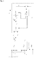
- Figure 1 shows a flow diagram of an exemplary implementation of a method according to the improved concept.
- the electric or electronic system comprises a power converter with a power semiconductor device.
- the following discussion with respect to Figure 1 applies analogously for other types of electric or electronic systems, as explained for example with respect to Figure 3 .
- the power converter During the operation of the power converter, one or more characteristic parameters of the system are measured.
- a reference temperature T b of the power converter and plurality of electrical parameters of the power converter including a total off-state duration t off of the power semiconductor device, a total on-state duration t on of the power semiconductor device, an on-state current I on of the power semiconductor device, an off-state voltage V off of the power semiconductor device and an on-state voltage V on of the power semiconductor device is measured within a predetermined measurement interval of duration T i .
- a switching power loss P SW is determined from the on- and off-state durations t on , t off , the on-state current I on , and the off-state voltage V off .
- a conduction power loss P cond is determined from the on- and off-state durations t on , t off , the on-state current I on , and the on-state voltage V on , for example according to the relation.
- the conduction power loss P cond and the switching power P SW loss may be added up and their sum may be used as an input for a thermal model M_th.
- the sum corresponds to a power dissipation due to self-heating P sh of the power semiconductor device.
- a cross-coupling power dissipation P cc due to further devices of the power converter, which may affect the junction temperature T j of the power semiconductor device may be determined and used as an additional input to the thermal model M_th.
- An output of the thermal model M_th may represent a temperature difference T j-b between the junction temperature T j and the reference temperature T b , which may for example be a baseplate temperature or a temperature of an internal thermistor of the of the power converter. Therefore, the reference temperature T b may be added to the output of the thermal model M_th, resulting in an estimate for the junction temperature T j .
- the estimated junction temperature T j may be used as an input to a TSEP model M_TSEP.
- An output of the TSEP model M_TSEP represents a first value V1 for one or more TSEPs of the power converter, in particular the power semiconductor device.
- the one or more TSEPs may include the on-state voltage V on , a gate threshold voltage, an internal gate resistance and/or a characteristic switching parameter of the power semiconductor device.
- the TSEP model M_TSEP may for example use the fact that, in a steady state of the power semiconductor device, a rate of change of the junction temperature T j is equal to a rate of change of the reference temperature T b for a constant power dissipation. Therefore, the junction temperature T j may follow the reference temperature T b with an offset. The offset may correspond to a respective thermal resistance multiplied by the constant power dissipation. Furthermore, also the on-state voltage V on follows the rate of temperature change, albeit with a scale factor.
- a second value V2 for the one or more TSEPs is obtained from a subset of the measured parameters, in the shown example from the on-state current I on and/or the on-state voltage V on (see calculation block CALC).
- the second value V2 depends only on the on-state voltage V on or may be equal to the on-state voltage V on . In the latter case, no calculation step CALC is necessary.
- the on-state current I on and the calculation step CALC may be necessary.
- Respective first and second values V1, V2 of the TSEPs are compared to each other, in particular respective differences are determined.
- thermal parameters P_th of the thermal model M_th and/or TSEP parameters P_TSEP of the TSEP model M_TSEP are adapted and used to adapt the models M_th, M_TSEP accordingly.
- the junction temperature T j may be considered as a final result of the junction temperature determination. Otherwise, the junction temperature T j may be determined again based on the adapted models M_th, M_TSEP and so forth.
- Figure 2A shows a block diagram of an exemplary embodiment of an electric or electronic system according to the improved concept.
- the system comprises a power converter PC containing one or more (for simplicity only one is shown) power semiconductor devices PS, for example IGBTs, BJTs, MOSFETs, HEMTs, JFETs, thyristors or diodes.
- power semiconductor devices PS for example IGBTs, BJTs, MOSFETs, HEMTs, JFETs, thyristors or diodes.
- IGBTs for example IGBTs, BJTs, MOSFETs, HEMTs, JFETs, thyristors or diodes.
- the circuit symbol of an IGBT is shown in Figure 2A only as a non-limiting example.
- the power converter PC further comprises a measuring unit MU for determining electrical parameters of the power converter PC, in particular of the power semiconductor device PS, including for example one or more of the measured parameters explained with respect to Figure 1 .
- the power converter PC also comprises a computing unit CU for performing one or more of the computational steps described with respect to Figure 1 .
- the computing unit CU and the measuring unit MU may for example be comprised by a drive unit (not shown) or a control unit (not shown) of the power converter PC or may be part of a separate circuit (not shown) of the power converter PC.
- Figure 2B shows a block diagram of a further exemplary embodiment of an electric or electronic system according to the improved concept.
- the system of Figure 2B is identical to the system of Figure 2A , except for the arrangement of the computing unit CU and the measuring unit MU.
- the computing unit CU and the measuring unit MU are not part of the power converter PC but are comprised by a circuit C coupled to the power converter PC.
- the circuit may for example comprise a microprocessor (not shown) including the computing unit CU.
- Figure 3 shows a block diagram of a further exemplary embodiment of an electric or electronic system according to the improved concept.
- the system comprises a power transformer or a reactor, in particular a shunt reactor, with a tank T.
- a power transformer or a reactor in particular a shunt reactor
- One or more windings W1, W2, W3 are arranged within the tank T.
- the tank T may for example for be filled or partly filled with an insulation agent IM, for example a transformer oil.
- the characteristic temperature is a winding temperature or hot spot temperature of one of the windings W1, W2, W3.
- the winding temperature replaces the junction temperature Tj.
- An ambient temperature of the transformer or reactor or a temperature of the insulation agent IM may replace the base plate temperature T b of Figure 1 .
- the total on- and off-state durations t on , t off , as well as the on- and off-state voltages V on , V off and the on-state current I on of Figure 1 may be replaced by appropriate quantities affecting the power dissipation of the transformer or reactor.
- all necessary inputs to a thermal model M_th of the transformer or reactor are case dependent and known or straight forwardly derivable to the skilled reader.
- the TSEP for which the first and the second values V1, V2 are determined may be replaced by any temperature-sensitive parameter of the transformer or rector, for example an electrical resistance of one of the windings W1, W2, W3.
- the improved concept By means of a method or a system according to the improved concept, it is possible to determine the characteristic temperature of an electric or electronic system without prior calibration and during normal operation of the system. This is achieved by using a hybrid approach of simulation and estimation. Forcing the determined values for the TSEP to match results in the whole system being characterized based on easily accessible quantities.
- the improved concept is widely applicable to many kinds of electric or electronic systems, which requires merely a suitable choice of parameters.
- Another advantage of the improved concept is that no prior knowledge of the device characteristics is required except for an approximate estimate of the TSEP characteristics.
- the latter may depend on a mathematical model being used, including least square fitting, adaptive filtering, Kalman filtering and principal components analysis. Datasheet parameters may also be sufficient.
- Implementations according to the improved concept may involve junction temperature estimation of a power semiconductor device, which may enable several features in next generation of "smart" power converters, including: dynamic rating control (intelligent over-rate/de-rate), optimized parallel inverter stack current sharing, condition monitoring (detection of wear-out and abnormal operation, giving predictive maintenance), temperature cycle counting and remaining useful life estimation, improved validation of inverter stack design during development and type testing, improved over-temperature detection.
- dynamic rating control intelligent over-rate/de-rate
- optimized parallel inverter stack current sharing condition monitoring (detection of wear-out and abnormal operation, giving predictive maintenance)
- temperature cycle counting and remaining useful life estimation
- improved validation of inverter stack design during development and type testing improved over-temperature detection.
- Resulting benefits to manufacturers of power converters may include an optimized performance (for example current rating or efficiency) versus costs, for example through reduction of margins.
- Benefits to the end users of power converters may include the early detection of abnormal operation and potentially reduced operating costs.
- an on-state voltage drop or a gate threshold voltage of an IGBT may have a variation range of ⁇ 100 mV or even more for 95% of production batches.
- an on-state voltage drop or a gate threshold voltage of an IGBT may have a variation range of ⁇ 100 mV or even more for 95% of production batches.
Landscapes
- Physics & Mathematics (AREA)
- General Physics & Mathematics (AREA)
- Power Conversion In General (AREA)
Abstract
Description
- The invention relates to a method for determining a characteristic temperature of an electric or electronic system and to an electric or electronic system.
- In electric or electronic systems or devices, specific characteristic temperatures may be of particular interest due to their effects for example on reliability, lifetime or rate of degradation. In some cases, a characteristic temperature exceeding a certain absolute limit can also lead to the destruction of the device or system. Therefore, it may be vital or at least desirable to determine or monitor a characteristic temperature during operation of the system or device.
- However, in many situations a direct measurement of the characteristic temperature of interest may be impractical or not feasible, for example due to a harsh environment. In particular, this may be the case for junction temperatures of power semiconductor devices, since during operation they typically are electrically "live" and in a highly noisy environment. Other examples include a winding temperature of a power transformer or reactor or a characteristic temperature within an on-load tap changer, for example a resistor temperature.
- Existing approaches to an indirect estimation of such characteristic temperatures require a prior calibration of each individual system or device, which is impractical in industrial applications and in particular virtually impossible in case of semiconductor devices. Other approaches require specific laboratory settings or dedicated operation modes of the system or device, in some cases also a specific compatible load.
- Therefore, it is an objective of the present invention to provide an improved concept for determining a characteristic temperature of an electric or electronic system that may be performed during normal operation of the system or device and does not require a calibration prior to the operation.
- This objective is achieved by the subject matter of the independent claims. Further implementations and embodiments are the subject matter of the dependent claims.
- The improved concept is based on the idea to implement an auto- or self-calibration of the system by estimating the characteristic temperature based on a thermal model of the system and predicting a first value of a temperature-sensitive electrical parameter, TSEP, of the system based on a TSEP model and an output of the thermal model. The first value is compared to a second value for the TSEP based on a measurement. The thermal and/or of the TSEP model are then adapted to match the two values for the TSEP.
- According to the improved concept, a method for determining a characteristic temperature of an electric or electronic system is provided. The method comprises measuring one or more characteristic parameters, in particular electric parameters and/or thermal parameters and/or temperatures, of the system during operation of the system and estimating the characteristic temperature of the system based on a thermal model of the system and on a first subset of the measured parameters. Then a first value for a TSEP is predicted based on a TSEP model and on the estimated characteristic temperature. A second value for the TSEP is determined based on a second subset of the measured parameters. Then, the first value for the TSEP is compared to the second value for the TSEP and the thermal model and/or the TSEP model is adapted based on a result of the comparison.
- The first and the second subset may contain one or more parameters, respectively. The subsets may overlap or be disjoint. Alternatively, the subsets may be identical, in particular be identical and contain only one parameter, respectively.
- The TSEP model may be a pre-determined model. The same holds for the thermal model. The thermal model may contain a model for determining a thermal impedance of the system. The thermal model may for example be based on or include a finite-element method, a reduced-order model, a thermal resistor-capacitor network model. In particular, the reduced-order model or the thermal resistor-capacitor network model may be fitted to the finite-element model.
- Performing the method, in particular the measurements, during operation means performing it during a normal or productive operation for which the system is intended. In particular, it is neither necessarily performed during production of the system or device, in a test environment nor in a dedicated calibration mode of operation.
- In some implementations, the method comprises running the electric or electronic system or a part of it through a training sequence for example before an initial, in particular initial normal, operation of the system. The training sequence may improve a convergence of the auto-calibration according to the improved concept.
- The TSEP is a TSEP of the system, in particular of an electric or electronic device comprised by the system.
- The TSEP model being adapted may for example mean that parameters used to predict the TSEP based on the characteristic temperature, for example fit parameters or regression parameters, are adapted.
- The thermal model being adapted may for example mean that parameters used to determine the thermal impedance are adapted.
- Comparing the first and the second value for the TSEP may for example comprise determining a difference between these values. The result of the comparison may for example comprise the difference.
- By means of a method according to the improved concept as described, the drawbacks of both approaches, temperature simulation based on thermal modelling and temperature estimation based on a measured TSEP, are overcome. In particular, characteristic temperatures from both approaches are not compared but instead respective TSEP values are. In this way one gets rid of the need for calibrating the temperature estimation based on measured TSEPs. The accuracy of deducing the second value for the TSEP will not change throughout the lifetime of the system and therefore will track correctly any changes in electrical and thermal parameters, for example due to degradation or measurement circuit drift. On the other hand, deducing the first value for the TSEP will correctly reflect ambient temperature or other temperatures of the system affecting the characteristic temperature and for example power losses of the system. This can be viewed as using the thermal model to calibrate the TSEPs, or using the measurements to keep the thermal model tracking correctly. Either way, the full electro-thermal system is characterized, namely both an effective electrical calibration and a thermal characterization.
- A final result of the method may for example be given by the characteristic temperature which will be valid in case of matching first and second value for the TSEP.
- According to several embodiments, the method comprises predicting a first value for a further TSEP, in particular of the system or a device of the system, based on a further TSEP model and the estimated characteristic temperature. A second value for the further TSEP is determined based on the second subset of the measured parameters. The first value for the further TSEP is compared to the second value for the further TSEP. The adaption of the thermal model or the TSEP model is based on a result of the comparison of the first value and the second value for the further TSEP as well as on the result of the comparison of the first value and the second value for the TSEP.
- Matching two independent TSEPs by adapting said models may further improve the accuracy of the temperature estimation.
- According to several embodiments, the method further comprises repeating at least the steps of measuring the characteristic parameters, estimating the characteristic temperature and predicting the first value for the characteristic temperature. For the repetition, the adapted thermal model is used instead of the thermal model and/or the adapted TSEP model is used instead of the TSEP model.
- In order to improve the temperature estimation, the repeated steps may be repeated several times. For each repetition, the adapted thermal or TSEP model of the preceding repetition is used. For example, the repeated steps may be repeated until the difference between the first and the second value for the TSEP is smaller than a predefined threshold and, if applicable, the difference between the first and the second value for the further TSEP is smaller than a predefined further threshold.
- According to several embodiments, the characteristic temperature is a characteristic temperature of an electric or electronic device comprised by the system.
- According to several embodiments, the electric or electronic system is a power electronic system, for example a power converter, and the characteristic temperature is a characteristic temperature, in particular a junction temperature, of a power semiconductor device comprised by the system.
- According to several embodiments, the first subset of the one or more measured characteristic parameters comprises an on-state, that is forward, current of the power semiconductor device and/or an on-state, that is forward, voltage of the power semiconductor device and/or an off-state voltage of the power semiconductor device and/or a total on-state duration of the power semiconductor device within a respective measurement interval and/or a total off-state duration of the power semiconductor device within the respective measurement interval and/or a reference temperature of the power electronic system.
- According to several embodiments, the reference temperature is a baseplate temperature or a thermistor temperature of the power electronic system.
- According to several embodiments, the second subset of the one or more measured characteristic parameters comprises the on-state current and/or the on-state voltage of the power semiconductor device.
- According to several embodiments, the TSEP and/or the further TSEP is given by the on-state voltage of the power semiconductor device, in particular at a predefined on-state current of the power semiconductor device, a gate threshold voltage of the power semiconductor device, an internal gate resistance of the power semiconductor device or a characteristic switching parameter of the power semiconductor device, in particular at a predefined on-state voltage or off-state voltage or on-state current.
- In some implementations, the characteristic switching parameter is given by a rate of change of current with respect to time di/dt, a rate of change of voltage with respect to time dv/dt, a switching peak current or a switching peak voltage.
- According to several embodiments, the step of estimating the characteristic temperature comprises determining a power dissipation due to the device and using the power dissipation as an input to the thermal model.
- According to several embodiments, the power dissipation comprises a switching power dissipation and/or a conduction power dissipation of the power semiconductor device.
- According to several embodiments, the step of estimating the characteristic temperature comprises determining a cross-coupling power dissipation due to a further device or several further devices of the system and using the cross-coupling power dissipation as an input, in particular a further input, to the thermal model.
- According to the improved concept, also an electric or electronic system is provided. The system comprises an electric or electronic device, a measuring unit and a computing unit. The measuring unit is configured to measure one or more characteristic parameters of the device during operation of the electric or electronic system.
- The computing unit is configured to estimate a characteristic temperature of the device based on a thermal model of the system and a first subset of the measured parameters, to predict a first value for a TSEP based on a TSEP model and the estimated characteristic temperature, to determine a second value for the TSEP based on a second subset of the measured parameters, to compare the first value and the second value for the TSEP and to adapt the thermal model or the TSEP model based on a result of the comparison.
- According to several embodiments, the electric or electronic system comprises a transformer, in particular a power transformer, for example filled with an insulation agent, in particular a liquid insulation agent. The electric or electronic device comprises a winding of the transformer and the characteristic temperature is given by a winding temperature, in particular a hot spot winding temperature, of the transformer.
- According to several embodiments, the electric or electronic system comprises a reactor, for example a shunt reactor, or an inductor for example filled with an isolation medium. The electric or electronic device comprises a winding of the reactor and the characteristic temperature is given by a winding temperature, in particular a hot spot winding temperature, of the reactor.
- According to several embodiments, the electric or electronic system comprises an on-load tap changer, for example an on-load tap changer of the resistor type. The characteristic temperature is given by a temperature within the on-load tap changer, for example a temperature of a resistor of the on-load tap-changer.
- According to several embodiments, the electric or electronic system comprises a power electronic system and the electric or electronic device comprises a power semiconductor device. The characteristic temperature is given by a junction temperature of the power semiconductor device.
- According to several embodiments, the power semiconductor comprises a transistor, for example an insulated-gate bipolar transistor, IGBT, or a bipolar junction transistor, BJT, or a MOS field effect transistor, MOSFET, or a junction field effect transistor, JFET, or a high-electron-mobility transistor, HEMT.
- According to several embodiments, the power semiconductor comprises a thyristor or a diode, for example a Schottky diode or a PIN diode.
- According to several embodiments, the power electronic system comprises a power converter and the power converter comprises the power semiconductor device.
- According to several embodiments, the power electronic system comprises a solid-state circuit breaker, a solid-state relay, a thyristor switch or a static VAR compensator, which comprises the power semiconductor device.
- Further implementations and embodiments of the electric or electronic system according to the improved concept follow readily from the various implementations and embodiments of the method according to the improved concept and vice versa. In particular, individual or several components or arrangements described with respect to the electric or electronic system may be implemented accordingly for performing a method according to the improved system.
- In the following, the invention is explained in detail with respect to exemplary implementations by reference to the drawings. Components that are functionally identical or have an identical effect may be denoted by identical reference signs. Identical components or components with identical functions or effects may be described only with respect to the figure where they occur first. Their description is not necessarily repeated in subsequent figures.
- In the drawings,
- Figure 1
- shows a flow diagram of an exemplary implementation of a method according to the improved concept;
- Figure 2A
- shows a block diagram of an exemplary embodiment of an electric or electronic system according to the improved concept;
- Figure 2B
- shows a block diagram of a further exemplary embodiment of an electric or electronic system according to the improved concept; and
- Figure 3
- shows a block diagram of a further exemplary embodiment of an electric or electronic system according to the improved concept.
-
Figure 1 shows a flow diagram of an exemplary implementation of a method according to the improved concept. - In the shown exemplary and non-limiting case, the electric or electronic system comprises a power converter with a power semiconductor device. The following discussion with respect to
Figure 1 , however, applies analogously for other types of electric or electronic systems, as explained for example with respect toFigure 3 . During the operation of the power converter, one or more characteristic parameters of the system are measured. In the shown example, a reference temperature Tb of the power converter and plurality of electrical parameters of the power converter including a total off-state duration toff of the power semiconductor device, a total on-state duration ton of the power semiconductor device, an on-state current Ion of the power semiconductor device, an off-state voltage Voff of the power semiconductor device and an on-state voltage Von of the power semiconductor device is measured within a predetermined measurement interval of duration Ti. - For example, a switching power loss PSW is determined from the on- and off-state durations ton, toff, the on-state current Ion, and the off-state voltage Voff.
- For example, a conduction power loss Pcond is determined from the on- and off-state durations ton, toff, the on-state current Ion, and the on-state voltage Von, for example according to the relation.
- The conduction power loss Pcond and the switching power PSW loss may be added up and their sum may be used as an input for a thermal model M_th. The sum corresponds to a power dissipation due to self-heating Psh of the power semiconductor device. Optionally, a cross-coupling power dissipation Pcc due to further devices of the power converter, which may affect the junction temperature Tj of the power semiconductor device may be determined and used as an additional input to the thermal model M_th.
- An output of the thermal model M_th may represent a temperature difference Tj-b between the junction temperature Tj and the reference temperature Tb, which may for example be a baseplate temperature or a temperature of an internal thermistor of the of the power converter. Therefore, the reference temperature Tb may be added to the output of the thermal model M_th, resulting in an estimate for the junction temperature Tj.
- Then, the estimated junction temperature Tj may be used as an input to a TSEP model M_TSEP. An output of the TSEP model M_TSEP represents a first value V1 for one or more TSEPs of the power converter, in particular the power semiconductor device. The one or more TSEPs may include the on-state voltage Von, a gate threshold voltage, an internal gate resistance and/or a characteristic switching parameter of the power semiconductor device.
- The TSEP model M_TSEP may for example use the fact that, in a steady state of the power semiconductor device, a rate of change of the junction temperature Tj is equal to a rate of change of the reference temperature Tb for a constant power dissipation. Therefore, the junction temperature Tj may follow the reference temperature Tb with an offset. The offset may correspond to a respective thermal resistance multiplied by the constant power dissipation. Furthermore, also the on-state voltage Von follows the rate of temperature change, albeit with a scale factor.
- A second value V2 for the one or more TSEPs is obtained from a subset of the measured parameters, in the shown example from the on-state current Ion and/or the on-state voltage Von (see calculation block CALC). In a simple example, the second value V2 depends only on the on-state voltage Von or may be equal to the on-state voltage Von. In the latter case, no calculation step CALC is necessary. However, in alternative cases of more complex TSEPs, for example switching parameters of the power semiconductor device, also the on-state current Ion and the calculation step CALC may be necessary.
- Respective first and second values V1, V2 of the TSEPs are compared to each other, in particular respective differences are determined. Depending on the differences, thermal parameters P_th of the thermal model M_th and/or TSEP parameters P_TSEP of the TSEP model M_TSEP are adapted and used to adapt the models M_th, M_TSEP accordingly.
- In case the differences between the first and second values V1, V2 are sufficiently small, for example all lie below respective threshold values, the junction temperature Tj may be considered as a final result of the junction temperature determination. Otherwise, the junction temperature Tj may be determined again based on the adapted models M_th, M_TSEP and so forth.
-
Figure 2A shows a block diagram of an exemplary embodiment of an electric or electronic system according to the improved concept. - The system comprises a power converter PC containing one or more (for simplicity only one is shown) power semiconductor devices PS, for example IGBTs, BJTs, MOSFETs, HEMTs, JFETs, thyristors or diodes. The circuit symbol of an IGBT is shown in
Figure 2A only as a non-limiting example. - The power converter PC further comprises a measuring unit MU for determining electrical parameters of the power converter PC, in particular of the power semiconductor device PS, including for example one or more of the measured parameters explained with respect to
Figure 1 . - The power converter PC also comprises a computing unit CU for performing one or more of the computational steps described with respect to
Figure 1 . - The computing unit CU and the measuring unit MU may for example be comprised by a drive unit (not shown) or a control unit (not shown) of the power converter PC or may be part of a separate circuit (not shown) of the power converter PC.
-
Figure 2B shows a block diagram of a further exemplary embodiment of an electric or electronic system according to the improved concept. - The system of
Figure 2B is identical to the system ofFigure 2A , except for the arrangement of the computing unit CU and the measuring unit MU. In particular, the computing unit CU and the measuring unit MU are not part of the power converter PC but are comprised by a circuit C coupled to the power converter PC. The circuit may for example comprise a microprocessor (not shown) including the computing unit CU. -
Figure 3 shows a block diagram of a further exemplary embodiment of an electric or electronic system according to the improved concept. - The system comprises a power transformer or a reactor, in particular a shunt reactor, with a tank T. One or more windings W1, W2, W3 are arranged within the tank T. The tank T may for example for be filled or partly filled with an insulation agent IM, for example a transformer oil.
- In such a system, the characteristic temperature is a winding temperature or hot spot temperature of one of the windings W1, W2, W3.
- With respect to the discussion of
Figure 1 , the winding temperature replaces the junction temperature Tj. An ambient temperature of the transformer or reactor or a temperature of the insulation agent IM may replace the base plate temperature Tb ofFigure 1 . The total on- and off-state durations ton, toff, as well as the on- and off-state voltages Von, Voff and the on-state current Ion ofFigure 1 may be replaced by appropriate quantities affecting the power dissipation of the transformer or reactor. In fact, all necessary inputs to a thermal model M_th of the transformer or reactor are case dependent and known or straight forwardly derivable to the skilled reader. The TSEP for which the first and the second values V1, V2 are determined may be replaced by any temperature-sensitive parameter of the transformer or rector, for example an electrical resistance of one of the windings W1, W2, W3. - With these or other suitable replacements, the method described with respect to
Figure 1 may also be carried out analogously for the transformer or reactor. - With respective suitable replacements, the method described with respect to
Figure 1 may also be carried out analogously for an on-load tap changer. - By means of a method or a system according to the improved concept, it is possible to determine the characteristic temperature of an electric or electronic system without prior calibration and during normal operation of the system. This is achieved by using a hybrid approach of simulation and estimation. Forcing the determined values for the TSEP to match results in the whole system being characterized based on easily accessible quantities. The improved concept is widely applicable to many kinds of electric or electronic systems, which requires merely a suitable choice of parameters.
- An effective re-calibration of system or device temperature sensitivity throughout the life of the system is achieved. Therefore, long-term changes in electrical and thermal parameters are tracked throughout the lifetime of the device, meaning that a condition monitoring is inherently provided.
- Another advantage of the improved concept is that no prior knowledge of the device characteristics is required except for an approximate estimate of the TSEP characteristics. The latter may depend on a mathematical model being used, including least square fitting, adaptive filtering, Kalman filtering and principal components analysis. Datasheet parameters may also be sufficient.
- In case of power converters, no changes to power converter modules are required, in particular no extra connections or sensors within the module are required.
- Implementations according to the improved concept may involve junction temperature estimation of a power semiconductor device, which may enable several features in next generation of "smart" power converters, including: dynamic rating control (intelligent over-rate/de-rate), optimized parallel inverter stack current sharing, condition monitoring (detection of wear-out and abnormal operation, giving predictive maintenance), temperature cycle counting and remaining useful life estimation, improved validation of inverter stack design during development and type testing, improved over-temperature detection.
- Resulting benefits to manufacturers of power converters may include an optimized performance (for example current rating or efficiency) versus costs, for example through reduction of margins. Benefits to the end users of power converters may include the early detection of abnormal operation and potentially reduced operating costs.
- To demonstrate the effect of lacking calibration in case the improved concept is not utilized, product variations of an IGBT for use in a power converter are considered as an example. Typically, an on-state voltage drop or a gate threshold voltage of an IGBT may have a variation range of ±100 mV or even more for 95% of production batches. When combined with a typical TSEP sensitivity of 1-10 mV/K this gives an error in the range of 10-100 °C which would make junction temperature estimation pointless. This highlights the benefits of the improved concept.
-
- Tb
- base plate temperature
- ton
- total on-state duration
- toff
- total off-state duration
- Ion
- on-state current
- Von
- on-state voltage
- Voff
- off-state voltage
- Tj
- junction temperature
- Tj-b
- temperature difference
- PSW
- switching power loss
- Pcond
- conduction power loss
- Psh
- self-heating power dissipation
- Pcc
- cross-coupling power dissipation
- V1, V2
- values for the TSEP
- M_th
- thermal model
- M_TSEP
- TSEP model
- CALC
- calculation step
- P_th
- thermal parameters
- P_TSEP
- TSEP parameters
- PC
- power converter
- CU
- computing unit
- MU
- measuring unit
- C
- circuit
- PS
- power semiconductor device
- T
- tank
- IM
- insulation agent
- W1, W2, W3
- windings of transformer or reactor
Claims (15)
- Method for determining a characteristic temperature (Tj) of an electric or electronic system, wherein the method comprises- during operation of the system, measuring one or more characteristic parameters of the system;- estimating the characteristic temperature (Tj) based on a thermal model (M_th) of the system and a first subset of the measured parameters;- predicting a first value (V1) for a temperature-sensitive electrical parameter, TSEP, based on a TSEP model (M_TSEP) and the estimated characteristic temperature (Tj) ;- determining a second value (V2) for the TSEP based on a second subset of the measured parameters;- comparing the first value (V1) and the second value (V2) for the TSEP; and- adapting the thermal model (M_th) or the TSEP model (M_TSEP) based on a result of the comparison.
- Method according to claim 1, comprising- predicting a first value (V1) for a further TSEP based on a further TSEP model and the estimated characteristic temperature (Tj) ;- determining a second value (V2) for the further TSEP based on the second subset of the measured parameters;- comparing the first value (V1) and the second value (V2) for the further TSEP;- wherein the adaption of the thermal model (M_th) or the TSEP model (M_TSEP) is based on a result of the comparison of the first value (V1) and the second value (V2) for the further TSEP.
- Method according to one of claims 1 or 2, wherein- the method further comprises repeating at least the steps of measuring the characteristic parameters, estimating the characteristic temperature (Tj) and predicting the first value (V1) for the TSEP; and- for the repetition, the adapted thermal model is used instead of the thermal model (M_th) and/or the adapted TSEP model is used instead of the TSEP model (M_TSEP).
- Method according to one of claims 1 to 3, wherein the characteristic temperature (Tj) is a characteristic temperature (Tj) of an electric or electronic device comprised by the system.
- Method according to claim 4, wherein- the system is a power electronic system; and- the characteristic temperature (Tj) is a characteristic temperature (Tj), in particular a junction temperature (Tj), of a power semiconductor device (PS) comprised by the system.
- Method according to claim 5, wherein the first subset comprises at least one of the following parameters:- an on-state current (Ion) of the power semiconductor device (PS);- an on-state voltage (Von) of the power semiconductor device (PS);- an off-state voltage (Voff) of the power semiconductor device (PS) ;- a total on-state duration (ton) of the power semiconductor device (PS) within a respective measurement interval;- a total off-state duration (toff) of the power semiconductor device (PS) within the respective measurement interval;- a reference temperature (Tb) of the power electronic system.
- Method according to one of claims 5 or 6, wherein the second subset comprises an on-state current (Ion) and/or an on-state voltage (Von) of the power semiconductor device (PS).
- Method according to one of claims 5 to 7, wherein the TSEP is given by- an on-state voltage (Von) of the power semiconductor device (PS), in particular at a predefined on-state current (Ion) of the power semiconductor device (PS); or- a gate threshold voltage of the power semiconductor device (PS); or- an internal gate resistance of the power semiconductor device (PS) ; or- a characteristic switching parameter of the power semiconductor device (PS), in particular at a predefined on-state voltage (Von) or off-state voltage (Voff) or on-state current (Ion).
- Method according to one of claims 4 to 8, wherein the step of estimating the characteristic temperature (Tj) comprises- determining a power dissipation (Psh) due to the device (PS); and- using the power dissipation (Psh) as an input to the thermal model (M_th).
- Method according to claims 5 and 9, wherein the power dissipation (Psh) comprises a switching power dissipation (PSW) or a conduction power dissipation (Pcond) of the power semiconductor device (PS).
- Method according to one of claims 4 to 10, wherein the step of estimating the characteristic temperature (Tj) comprises- determining a cross-coupling power dissipation (Pcc) due to a further device of the system; and- using the cross-coupling power dissipation (Pcc) as an input to the thermal model (M_th).
- Electric or electronic system comprising- an electric or electronic device;- a measuring unit (MU) configured to measure one or more characteristic parameters of the device during operation of the system;- a computing unit (CU) configured to- estimate a characteristic temperature (Tj) of the device based on a thermal model (M_th) of the system and a first subset of the measured parameters;- predict a first value (V1) for a temperature sensitive electrical parameter, TSEP, based on a TSEP model (M_TSEP) and the estimated characteristic temperature (Tj) ;- determine a second value (V2) for the TSEP based on a second subset of the measured parameters;- compare the first value (V1) and the second value (V2) for the TSEP; and- adapt the thermal model (M_th) or the TSEP model (M_TSEP) based on a result of the comparison.
- System according to claim 12 comprising a power transformer or a reactor, wherein- the device comprises a winding (W1, W2, W3) of the transformer or reactor; and- the characteristic temperature (Tj) is given by a winding temperature of the transformer or reactor.
- System according to claim 12 comprising a power electronic system, wherein- the device comprises a power semiconductor device (PS); and- the characteristic temperature (Tj) is given by a junction temperature (Tj) of the power semiconductor device (PS).
- System according to claim 14, wherein- the power electronic system comprises a power converter (PC); and- the power semiconductor device (PS) is comprised by the power converter (PC).
Priority Applications (6)
| Application Number | Priority Date | Filing Date | Title |
|---|---|---|---|
| EP18196070.9A EP3627121B1 (en) | 2018-09-21 | 2018-09-21 | Determining a characteristic temperature of an electric or electronic system |
| KR1020217011735A KR102855015B1 (en) | 2018-09-21 | 2019-09-19 | Method for determining characteristic temperatures of electrical or electronic systems |
| CN201980062221.2A CN112752960B (en) | 2018-09-21 | 2019-09-19 | Determine the characteristic temperature of an electrical or electronic system |
| JP2021515478A JP7414812B2 (en) | 2018-09-21 | 2019-09-19 | Determination of characteristic temperatures of electrical or electronic systems |
| US17/276,862 US11320321B2 (en) | 2018-09-21 | 2019-09-19 | Determining a characteristic temperature of an electric or electronic system |
| PCT/EP2019/075227 WO2020058435A1 (en) | 2018-09-21 | 2019-09-19 | Determining a characteristic temperature of an electric or electronic system |
Applications Claiming Priority (1)
| Application Number | Priority Date | Filing Date | Title |
|---|---|---|---|
| EP18196070.9A EP3627121B1 (en) | 2018-09-21 | 2018-09-21 | Determining a characteristic temperature of an electric or electronic system |
Publications (2)
| Publication Number | Publication Date |
|---|---|
| EP3627121A1 true EP3627121A1 (en) | 2020-03-25 |
| EP3627121B1 EP3627121B1 (en) | 2022-07-06 |
Family
ID=63678540
Family Applications (1)
| Application Number | Title | Priority Date | Filing Date |
|---|---|---|---|
| EP18196070.9A Active EP3627121B1 (en) | 2018-09-21 | 2018-09-21 | Determining a characteristic temperature of an electric or electronic system |
Country Status (6)
| Country | Link |
|---|---|
| US (1) | US11320321B2 (en) |
| EP (1) | EP3627121B1 (en) |
| JP (1) | JP7414812B2 (en) |
| KR (1) | KR102855015B1 (en) |
| CN (1) | CN112752960B (en) |
| WO (1) | WO2020058435A1 (en) |
Cited By (3)
| Publication number | Priority date | Publication date | Assignee | Title |
|---|---|---|---|---|
| DE102020125533B3 (en) | 2020-09-30 | 2021-12-30 | Maschinenfabrik Reinhausen Gmbh | Device and system for the indirect temperature determination of a power transformer |
| WO2022003086A1 (en) * | 2020-07-03 | 2022-01-06 | Leoni Kabel Gmbh | Method for determining a dynamic temperature distribution over the cross section and the length of a high-current cable |
| EP4099031A1 (en) * | 2021-06-01 | 2022-12-07 | Maschinenfabrik Reinhausen GmbH | Method for monitoring an electrical or electronic system and a further system configured to perform the method |
Families Citing this family (5)
| Publication number | Priority date | Publication date | Assignee | Title |
|---|---|---|---|---|
| CN110874079B (en) * | 2018-08-30 | 2023-07-14 | Abb瑞士股份有限公司 | Method and system for monitoring the condition of an electric drive |
| CN115603604A (en) * | 2021-07-08 | 2023-01-13 | 法雷奥西门子新能源汽车德国有限责任公司(De) | Estimation of internal temperature of inverter and semiconductor switch |
| KR102772550B1 (en) * | 2021-09-30 | 2025-02-26 | 주식회사 아도반테스토 | Control device for controlling ATE (Automated Test Equipment), ATE, method for controlling ATE, method for operating ATE, and computer program for performing these methods including estimating or determining temperature |
| CN114674460A (en) * | 2022-04-02 | 2022-06-28 | 国网江苏省电力有限公司常州供电分公司 | Method and device for alarming abnormal temperature of reactor |
| CN115951140A (en) * | 2022-12-05 | 2023-04-11 | 博格华纳驱动系统(苏州)有限公司 | A method for diagnosing aging of power components |
Citations (2)
| Publication number | Priority date | Publication date | Assignee | Title |
|---|---|---|---|---|
| US20100030510A1 (en) * | 2008-08-04 | 2010-02-04 | Ingo Koehler | Method for determining the temperature of an electrical component with the aid of a temperature model |
| US20180017612A1 (en) * | 2015-02-03 | 2018-01-18 | Siemens Aktiengesellschaft | Method For Determining A Deterioration Of Power Semiconductor Modules As Well As A Device And Circuit Arrangement |
Family Cites Families (36)
| Publication number | Priority date | Publication date | Assignee | Title |
|---|---|---|---|---|
| US4525763A (en) * | 1983-11-30 | 1985-06-25 | General Electric Company | Apparatus and method to protect motors and to protect motor life |
| JPH0654572A (en) * | 1992-07-31 | 1994-02-25 | Omron Corp | Electric motor thermal protector |
| US6006168A (en) * | 1997-12-12 | 1999-12-21 | Digital Equipment Corporation | Thermal model for central processing unit |
| JP2001208798A (en) * | 2000-01-26 | 2001-08-03 | Mitsubishi Electric Corp | Semiconductor circuit test method and apparatus |
| JP2003018861A (en) | 2001-06-27 | 2003-01-17 | Nissan Motor Co Ltd | Inverter cooling control device |
| DE10132452B4 (en) * | 2001-07-04 | 2005-07-28 | Robert Bosch Gmbh | Apparatus and method for measuring operating temperatures of an electrical component |
| JP2003315305A (en) * | 2002-04-22 | 2003-11-06 | Honda Motor Co Ltd | Temperature control device for exhaust gas sensor |
| US7570074B2 (en) * | 2005-05-09 | 2009-08-04 | Square D Company | Electronic overload relay for mains-fed induction motors |
| JP2006329869A (en) | 2005-05-27 | 2006-12-07 | Yamatake Corp | Temperature estimation device, temperature control device, temperature estimation method, temperature control method, temperature estimation program, and temperature control program |
| DE102007007988A1 (en) * | 2007-02-17 | 2008-08-28 | Robert Bosch Gmbh | Method and apparatus for friction compensation |
| ATE449992T1 (en) * | 2007-03-22 | 2009-12-15 | Baumueller Nuernberg Gmbh | TEMPERATURE MONITORING FOR CIRCUIT BREAKERS |
| JP5317881B2 (en) * | 2009-08-05 | 2013-10-16 | 三菱電機株式会社 | Power converter and protection method for power converter |
| EP2354864A1 (en) * | 2010-01-29 | 2011-08-10 | Eurocopter Deutschland GmbH | Method and system for an optimized utilization of energy resources of an electrical system |
| US8483982B2 (en) * | 2010-11-02 | 2013-07-09 | Schneider Electric USA, Inc. | Automated emergency power supply test using variable load bank stages |
| EP2568268A1 (en) * | 2011-09-07 | 2013-03-13 | kk-electronic a/s | Method for estimating the temperature of a semiconductor chip |
| WO2015044205A1 (en) * | 2013-09-24 | 2015-04-02 | Abb Technology Ag | Method and apparatus for determining an actual junction temperature of an igbt device |
| WO2015110107A2 (en) * | 2014-01-22 | 2015-07-30 | Schaeffler Technologies AG & Co. KG | Method for determining a temperature of an electric motor |
| FR3018557A1 (en) * | 2014-03-17 | 2015-09-18 | Peugeot Citroen Automobiles Sa | METHOD AND SYSTEM FOR ESTIMATING THE REMAINING TIME OF ACTIVATION OF A STARTER BEFORE OVERHEATING |
| US10001800B1 (en) * | 2015-09-10 | 2018-06-19 | Apple Inc. | Systems and methods for determining temperatures of integrated circuits |
| US10337932B2 (en) * | 2015-09-25 | 2019-07-02 | Oracle International Corporation | Adaptive method for calibrating multiple temperature sensors on a single semiconductor die |
| CN105825019B (en) * | 2016-03-22 | 2018-10-23 | 三峡大学 | A kind of insulated gate bipolar transistor IGBT module temperature derivation algorithm |
| KR102469942B1 (en) | 2016-04-19 | 2022-11-22 | 엘에스일렉트릭(주) | Apparatus for determining parameter when estimating temperature of switching element in inverter |
| US10985694B2 (en) * | 2016-07-15 | 2021-04-20 | Enphase Energy, Inc. | Method and apparatus for determining key performance photovoltaic characteristics using sensors from module-level power electronics |
| CN106443400B (en) * | 2016-09-14 | 2019-06-11 | 河北工业大学 | A method for establishing an electro-thermal-aging junction temperature calculation model for IGBT modules |
| US9971376B2 (en) * | 2016-10-07 | 2018-05-15 | Kilopass Technology, Inc. | Voltage reference circuits with programmable temperature slope and independent offset control |
| KR102712333B1 (en) * | 2016-12-15 | 2024-10-02 | 현대자동차주식회사 | Method for measuring junction temperature of power module |
| CN106844972A (en) * | 2017-01-22 | 2017-06-13 | 上海电力学院 | Transformer Winding temperature flexible measurement method based on PSO SVR |
| CN206760250U (en) * | 2017-02-10 | 2017-12-19 | 宁波海角信息科技有限公司 | Irrigation system |
| CN107219016B (en) * | 2017-05-24 | 2019-05-17 | 湖南大学 | Calculate the method and system of IGBT module transient state junction temperature |
| US10457263B2 (en) * | 2017-07-24 | 2019-10-29 | Bendix Commercial Vehicle Systems, Llc | Brake adjustment detection using WSS based thermal measurement |
| US10386899B2 (en) * | 2017-08-08 | 2019-08-20 | GM Global Technology Operations LLC | Methods and systems for configurable temperature control of controller processors |
| CN108038795B (en) * | 2017-12-05 | 2021-08-03 | 武汉大学 | Transformer hot spot temperature inversion method and system based on streamline and support vector machine |
| CN108072821B (en) * | 2017-12-06 | 2018-11-16 | 南京埃斯顿自动控制技术有限公司 | The real-time online prediction technique of semiconductor power device dynamic junction temperature |
| JP6973311B2 (en) * | 2018-07-03 | 2021-11-24 | オムロン株式会社 | Processing equipment |
| US10615737B1 (en) * | 2018-09-24 | 2020-04-07 | Nxp Usa, Inc. | System and method of estimating temperature of a power switch of a power converter without a dedicated sensor |
| JP7061060B2 (en) * | 2018-12-20 | 2022-04-27 | ルネサスエレクトロニクス株式会社 | Control circuit, drive system and inverter control method |
-
2018
- 2018-09-21 EP EP18196070.9A patent/EP3627121B1/en active Active
-
2019
- 2019-09-19 US US17/276,862 patent/US11320321B2/en active Active
- 2019-09-19 WO PCT/EP2019/075227 patent/WO2020058435A1/en not_active Ceased
- 2019-09-19 KR KR1020217011735A patent/KR102855015B1/en active Active
- 2019-09-19 CN CN201980062221.2A patent/CN112752960B/en active Active
- 2019-09-19 JP JP2021515478A patent/JP7414812B2/en active Active
Patent Citations (2)
| Publication number | Priority date | Publication date | Assignee | Title |
|---|---|---|---|---|
| US20100030510A1 (en) * | 2008-08-04 | 2010-02-04 | Ingo Koehler | Method for determining the temperature of an electrical component with the aid of a temperature model |
| US20180017612A1 (en) * | 2015-02-03 | 2018-01-18 | Siemens Aktiengesellschaft | Method For Determining A Deterioration Of Power Semiconductor Modules As Well As A Device And Circuit Arrangement |
Cited By (5)
| Publication number | Priority date | Publication date | Assignee | Title |
|---|---|---|---|---|
| WO2022003086A1 (en) * | 2020-07-03 | 2022-01-06 | Leoni Kabel Gmbh | Method for determining a dynamic temperature distribution over the cross section and the length of a high-current cable |
| DE102020125533B3 (en) | 2020-09-30 | 2021-12-30 | Maschinenfabrik Reinhausen Gmbh | Device and system for the indirect temperature determination of a power transformer |
| EP4208726B1 (en) | 2020-09-30 | 2024-08-21 | Maschinenfabrik Reinhausen GmbH | Device and system for indirectly determining the temperature of a power transformer |
| EP4099031A1 (en) * | 2021-06-01 | 2022-12-07 | Maschinenfabrik Reinhausen GmbH | Method for monitoring an electrical or electronic system and a further system configured to perform the method |
| WO2022253521A1 (en) * | 2021-06-01 | 2022-12-08 | Maschinenfabrik Reinhausen Gmbh | Method for monitoring an electrical or electronic system and a further system configured to perform the method |
Also Published As
| Publication number | Publication date |
|---|---|
| US20210318179A1 (en) | 2021-10-14 |
| JP2022501989A (en) | 2022-01-06 |
| KR20210063376A (en) | 2021-06-01 |
| WO2020058435A1 (en) | 2020-03-26 |
| CN112752960B (en) | 2024-05-17 |
| JP7414812B2 (en) | 2024-01-16 |
| US11320321B2 (en) | 2022-05-03 |
| CN112752960A (en) | 2021-05-04 |
| EP3627121B1 (en) | 2022-07-06 |
| KR102855015B1 (en) | 2025-09-03 |
Similar Documents
| Publication | Publication Date | Title |
|---|---|---|
| US11320321B2 (en) | Determining a characteristic temperature of an electric or electronic system | |
| JP2022501989A5 (en) | ||
| Ni et al. | Overview of real-time lifetime prediction and extension for SiC power converters | |
| US20240106381A1 (en) | Systems and methods for sensing temperature of inverter for electric vehicle | |
| EP3049779B1 (en) | Method and apparatus for determining an actual junction temperature of an igbt device | |
| US11262248B2 (en) | Analyzing an operation of a power semiconductor device | |
| Koenig et al. | On-line junction temperature measurement of CoolMOS devices | |
| US11852543B2 (en) | Method and electronic assembly for determining a temperature of at least one electronic switching element | |
| CN116609629B (en) | A health monitoring circuit and method for power semiconductor devices | |
| Yang et al. | A method of junction temperature estimation for SiC power MOSFETs via turn-on saturation current measurement | |
| KR101531018B1 (en) | Failure prediction method of power semiconductor device | |
| US12345754B2 (en) | Analyzing an operation of a power semiconductor device | |
| CN113711063A (en) | Power device monitoring system and monitoring method | |
| HK40048045A (en) | Determining a characteristic temperature of an electric or electronic system | |
| Boulzazen et al. | PHM method for detecting degradation of GaN HEMT ON resistance, application to power converter | |
| HK40052379A (en) | Analyzing an operation of a power semiconductor device | |
| HK40052379B (en) | Analyzing an operation of a power semiconductor device | |
| Yang | Methods for resolving the challenges of degradation diagnosis for SiC power MOSFET | |
| Asoodar et al. | Accurate ON-State Resistance Extraction for Online Condition Monitoring of Semiconductor Devices Under Noisy Conditions | |
| Chen | Machine Learning-based Reliability Monitoring of Power Semiconductor Devices | |
| Sengupta et al. | A Low-Cost Failure Detection Scheme for De-Energized MOSFET Switching Cells | |
| HK40047555A (en) | Analyzing an operation of a power semiconductor device | |
| HK40047555B (en) | Analyzing an operation of a power semiconductor device |
Legal Events
| Date | Code | Title | Description |
|---|---|---|---|
| PUAI | Public reference made under article 153(3) epc to a published international application that has entered the european phase |
Free format text: ORIGINAL CODE: 0009012 |
|
| STAA | Information on the status of an ep patent application or granted ep patent |
Free format text: STATUS: THE APPLICATION HAS BEEN PUBLISHED |
|
| AK | Designated contracting states |
Kind code of ref document: A1 Designated state(s): AL AT BE BG CH CY CZ DE DK EE ES FI FR GB GR HR HU IE IS IT LI LT LU LV MC MK MT NL NO PL PT RO RS SE SI SK SM TR |
|
| AX | Request for extension of the european patent |
Extension state: BA ME |
|
| STAA | Information on the status of an ep patent application or granted ep patent |
Free format text: STATUS: REQUEST FOR EXAMINATION WAS MADE |
|
| 17P | Request for examination filed |
Effective date: 20200925 |
|
| RBV | Designated contracting states (corrected) |
Designated state(s): AL AT BE BG CH CY CZ DE DK EE ES FI FR GB GR HR HU IE IS IT LI LT LU LV MC MK MT NL NO PL PT RO RS SE SI SK SM TR |
|
| GRAP | Despatch of communication of intention to grant a patent |
Free format text: ORIGINAL CODE: EPIDOSNIGR1 |
|
| STAA | Information on the status of an ep patent application or granted ep patent |
Free format text: STATUS: GRANT OF PATENT IS INTENDED |
|
| INTG | Intention to grant announced |
Effective date: 20220216 |
|
| GRAS | Grant fee paid |
Free format text: ORIGINAL CODE: EPIDOSNIGR3 |
|
| GRAA | (expected) grant |
Free format text: ORIGINAL CODE: 0009210 |
|
| STAA | Information on the status of an ep patent application or granted ep patent |
Free format text: STATUS: THE PATENT HAS BEEN GRANTED |
|
| AK | Designated contracting states |
Kind code of ref document: B1 Designated state(s): AL AT BE BG CH CY CZ DE DK EE ES FI FR GB GR HR HU IE IS IT LI LT LU LV MC MK MT NL NO PL PT RO RS SE SI SK SM TR |
|
| REG | Reference to a national code |
Ref country code: AT Ref legal event code: REF Ref document number: 1503174 Country of ref document: AT Kind code of ref document: T Effective date: 20220715 Ref country code: CH Ref legal event code: EP |
|
| REG | Reference to a national code |
Ref country code: DE Ref legal event code: R096 Ref document number: 602018037505 Country of ref document: DE |
|
| REG | Reference to a national code |
Ref country code: IE Ref legal event code: FG4D |
|
| REG | Reference to a national code |
Ref country code: LT Ref legal event code: MG9D |
|
| REG | Reference to a national code |
Ref country code: NL Ref legal event code: MP Effective date: 20220706 |
|
| PG25 | Lapsed in a contracting state [announced via postgrant information from national office to epo] |
Ref country code: SE Free format text: LAPSE BECAUSE OF FAILURE TO SUBMIT A TRANSLATION OF THE DESCRIPTION OR TO PAY THE FEE WITHIN THE PRESCRIBED TIME-LIMIT Effective date: 20220706 Ref country code: RS Free format text: LAPSE BECAUSE OF FAILURE TO SUBMIT A TRANSLATION OF THE DESCRIPTION OR TO PAY THE FEE WITHIN THE PRESCRIBED TIME-LIMIT Effective date: 20220706 Ref country code: PT Free format text: LAPSE BECAUSE OF FAILURE TO SUBMIT A TRANSLATION OF THE DESCRIPTION OR TO PAY THE FEE WITHIN THE PRESCRIBED TIME-LIMIT Effective date: 20221107 Ref country code: NO Free format text: LAPSE BECAUSE OF FAILURE TO SUBMIT A TRANSLATION OF THE DESCRIPTION OR TO PAY THE FEE WITHIN THE PRESCRIBED TIME-LIMIT Effective date: 20221006 Ref country code: NL Free format text: LAPSE BECAUSE OF FAILURE TO SUBMIT A TRANSLATION OF THE DESCRIPTION OR TO PAY THE FEE WITHIN THE PRESCRIBED TIME-LIMIT Effective date: 20220706 Ref country code: LV Free format text: LAPSE BECAUSE OF FAILURE TO SUBMIT A TRANSLATION OF THE DESCRIPTION OR TO PAY THE FEE WITHIN THE PRESCRIBED TIME-LIMIT Effective date: 20220706 Ref country code: LT Free format text: LAPSE BECAUSE OF FAILURE TO SUBMIT A TRANSLATION OF THE DESCRIPTION OR TO PAY THE FEE WITHIN THE PRESCRIBED TIME-LIMIT Effective date: 20220706 Ref country code: FI Free format text: LAPSE BECAUSE OF FAILURE TO SUBMIT A TRANSLATION OF THE DESCRIPTION OR TO PAY THE FEE WITHIN THE PRESCRIBED TIME-LIMIT Effective date: 20220706 Ref country code: ES Free format text: LAPSE BECAUSE OF FAILURE TO SUBMIT A TRANSLATION OF THE DESCRIPTION OR TO PAY THE FEE WITHIN THE PRESCRIBED TIME-LIMIT Effective date: 20220706 |
|
| REG | Reference to a national code |
Ref country code: AT Ref legal event code: MK05 Ref document number: 1503174 Country of ref document: AT Kind code of ref document: T Effective date: 20220706 |
|
| PG25 | Lapsed in a contracting state [announced via postgrant information from national office to epo] |
Ref country code: PL Free format text: LAPSE BECAUSE OF FAILURE TO SUBMIT A TRANSLATION OF THE DESCRIPTION OR TO PAY THE FEE WITHIN THE PRESCRIBED TIME-LIMIT Effective date: 20220706 Ref country code: IS Free format text: LAPSE BECAUSE OF FAILURE TO SUBMIT A TRANSLATION OF THE DESCRIPTION OR TO PAY THE FEE WITHIN THE PRESCRIBED TIME-LIMIT Effective date: 20221106 Ref country code: HR Free format text: LAPSE BECAUSE OF FAILURE TO SUBMIT A TRANSLATION OF THE DESCRIPTION OR TO PAY THE FEE WITHIN THE PRESCRIBED TIME-LIMIT Effective date: 20220706 Ref country code: GR Free format text: LAPSE BECAUSE OF FAILURE TO SUBMIT A TRANSLATION OF THE DESCRIPTION OR TO PAY THE FEE WITHIN THE PRESCRIBED TIME-LIMIT Effective date: 20221007 |
|
| REG | Reference to a national code |
Ref country code: DE Ref legal event code: R097 Ref document number: 602018037505 Country of ref document: DE |
|
| PG25 | Lapsed in a contracting state [announced via postgrant information from national office to epo] |
Ref country code: SM Free format text: LAPSE BECAUSE OF FAILURE TO SUBMIT A TRANSLATION OF THE DESCRIPTION OR TO PAY THE FEE WITHIN THE PRESCRIBED TIME-LIMIT Effective date: 20220706 Ref country code: RO Free format text: LAPSE BECAUSE OF FAILURE TO SUBMIT A TRANSLATION OF THE DESCRIPTION OR TO PAY THE FEE WITHIN THE PRESCRIBED TIME-LIMIT Effective date: 20220706 Ref country code: MC Free format text: LAPSE BECAUSE OF FAILURE TO SUBMIT A TRANSLATION OF THE DESCRIPTION OR TO PAY THE FEE WITHIN THE PRESCRIBED TIME-LIMIT Effective date: 20220706 Ref country code: DK Free format text: LAPSE BECAUSE OF FAILURE TO SUBMIT A TRANSLATION OF THE DESCRIPTION OR TO PAY THE FEE WITHIN THE PRESCRIBED TIME-LIMIT Effective date: 20220706 Ref country code: CZ Free format text: LAPSE BECAUSE OF FAILURE TO SUBMIT A TRANSLATION OF THE DESCRIPTION OR TO PAY THE FEE WITHIN THE PRESCRIBED TIME-LIMIT Effective date: 20220706 Ref country code: AT Free format text: LAPSE BECAUSE OF FAILURE TO SUBMIT A TRANSLATION OF THE DESCRIPTION OR TO PAY THE FEE WITHIN THE PRESCRIBED TIME-LIMIT Effective date: 20220706 |
|
| PLBE | No opposition filed within time limit |
Free format text: ORIGINAL CODE: 0009261 |
|
| STAA | Information on the status of an ep patent application or granted ep patent |
Free format text: STATUS: NO OPPOSITION FILED WITHIN TIME LIMIT |
|
| REG | Reference to a national code |
Ref country code: BE Ref legal event code: MM Effective date: 20220930 |
|
| PG25 | Lapsed in a contracting state [announced via postgrant information from national office to epo] |
Ref country code: SK Free format text: LAPSE BECAUSE OF FAILURE TO SUBMIT A TRANSLATION OF THE DESCRIPTION OR TO PAY THE FEE WITHIN THE PRESCRIBED TIME-LIMIT Effective date: 20220706 Ref country code: EE Free format text: LAPSE BECAUSE OF FAILURE TO SUBMIT A TRANSLATION OF THE DESCRIPTION OR TO PAY THE FEE WITHIN THE PRESCRIBED TIME-LIMIT Effective date: 20220706 |
|
| 26N | No opposition filed |
Effective date: 20230411 |
|
| PG25 | Lapsed in a contracting state [announced via postgrant information from national office to epo] |
Ref country code: LU Free format text: LAPSE BECAUSE OF NON-PAYMENT OF DUE FEES Effective date: 20220921 Ref country code: AL Free format text: LAPSE BECAUSE OF FAILURE TO SUBMIT A TRANSLATION OF THE DESCRIPTION OR TO PAY THE FEE WITHIN THE PRESCRIBED TIME-LIMIT Effective date: 20220706 |
|
| PG25 | Lapsed in a contracting state [announced via postgrant information from national office to epo] |
Ref country code: IE Free format text: LAPSE BECAUSE OF NON-PAYMENT OF DUE FEES Effective date: 20220921 |
|
| PG25 | Lapsed in a contracting state [announced via postgrant information from national office to epo] |
Ref country code: SI Free format text: LAPSE BECAUSE OF FAILURE TO SUBMIT A TRANSLATION OF THE DESCRIPTION OR TO PAY THE FEE WITHIN THE PRESCRIBED TIME-LIMIT Effective date: 20220706 |
|
| PG25 | Lapsed in a contracting state [announced via postgrant information from national office to epo] |
Ref country code: BE Free format text: LAPSE BECAUSE OF NON-PAYMENT OF DUE FEES Effective date: 20220930 |
|
| PG25 | Lapsed in a contracting state [announced via postgrant information from national office to epo] |
Ref country code: IT Free format text: LAPSE BECAUSE OF FAILURE TO SUBMIT A TRANSLATION OF THE DESCRIPTION OR TO PAY THE FEE WITHIN THE PRESCRIBED TIME-LIMIT Effective date: 20220706 |
|
| PG25 | Lapsed in a contracting state [announced via postgrant information from national office to epo] |
Ref country code: HU Free format text: LAPSE BECAUSE OF FAILURE TO SUBMIT A TRANSLATION OF THE DESCRIPTION OR TO PAY THE FEE WITHIN THE PRESCRIBED TIME-LIMIT; INVALID AB INITIO Effective date: 20180921 |
|
| PG25 | Lapsed in a contracting state [announced via postgrant information from national office to epo] |
Ref country code: CY Free format text: LAPSE BECAUSE OF FAILURE TO SUBMIT A TRANSLATION OF THE DESCRIPTION OR TO PAY THE FEE WITHIN THE PRESCRIBED TIME-LIMIT Effective date: 20220706 |
|
| PG25 | Lapsed in a contracting state [announced via postgrant information from national office to epo] |
Ref country code: MK Free format text: LAPSE BECAUSE OF FAILURE TO SUBMIT A TRANSLATION OF THE DESCRIPTION OR TO PAY THE FEE WITHIN THE PRESCRIBED TIME-LIMIT Effective date: 20220706 |
|
| PG25 | Lapsed in a contracting state [announced via postgrant information from national office to epo] |
Ref country code: TR Free format text: LAPSE BECAUSE OF FAILURE TO SUBMIT A TRANSLATION OF THE DESCRIPTION OR TO PAY THE FEE WITHIN THE PRESCRIBED TIME-LIMIT Effective date: 20220706 |
|
| PG25 | Lapsed in a contracting state [announced via postgrant information from national office to epo] |
Ref country code: BG Free format text: LAPSE BECAUSE OF FAILURE TO SUBMIT A TRANSLATION OF THE DESCRIPTION OR TO PAY THE FEE WITHIN THE PRESCRIBED TIME-LIMIT Effective date: 20220706 |
|
| PG25 | Lapsed in a contracting state [announced via postgrant information from national office to epo] |
Ref country code: MT Free format text: LAPSE BECAUSE OF FAILURE TO SUBMIT A TRANSLATION OF THE DESCRIPTION OR TO PAY THE FEE WITHIN THE PRESCRIBED TIME-LIMIT Effective date: 20220706 |
|
| REG | Reference to a national code |
Ref country code: CH Ref legal event code: U11 Free format text: ST27 STATUS EVENT CODE: U-0-0-U10-U11 (AS PROVIDED BY THE NATIONAL OFFICE) Effective date: 20251001 |
|
| PGFP | Annual fee paid to national office [announced via postgrant information from national office to epo] |
Ref country code: DE Payment date: 20250919 Year of fee payment: 8 |
|
| PGFP | Annual fee paid to national office [announced via postgrant information from national office to epo] |
Ref country code: GB Payment date: 20250923 Year of fee payment: 8 |
|
| PGFP | Annual fee paid to national office [announced via postgrant information from national office to epo] |
Ref country code: FR Payment date: 20250924 Year of fee payment: 8 |
|
| PGFP | Annual fee paid to national office [announced via postgrant information from national office to epo] |
Ref country code: CH Payment date: 20251001 Year of fee payment: 8 |