JP7061060B2 - Control circuit, drive system and inverter control method - Google Patents
Control circuit, drive system and inverter control method Download PDFInfo
- Publication number
- JP7061060B2 JP7061060B2 JP2018238768A JP2018238768A JP7061060B2 JP 7061060 B2 JP7061060 B2 JP 7061060B2 JP 2018238768 A JP2018238768 A JP 2018238768A JP 2018238768 A JP2018238768 A JP 2018238768A JP 7061060 B2 JP7061060 B2 JP 7061060B2
- Authority
- JP
- Japan
- Prior art keywords
- value
- inverter
- temperature
- power semiconductor
- circuit
- Prior art date
- Legal status (The legal status is an assumption and is not a legal conclusion. Google has not performed a legal analysis and makes no representation as to the accuracy of the status listed.)
- Active
Links
Images


Classifications
-
- H—ELECTRICITY
- H02—GENERATION; CONVERSION OR DISTRIBUTION OF ELECTRIC POWER
- H02M—APPARATUS FOR CONVERSION BETWEEN AC AND AC, BETWEEN AC AND DC, OR BETWEEN DC AND DC, AND FOR USE WITH MAINS OR SIMILAR POWER SUPPLY SYSTEMS; CONVERSION OF DC OR AC INPUT POWER INTO SURGE OUTPUT POWER; CONTROL OR REGULATION THEREOF
- H02M1/00—Details of apparatus for conversion
- H02M1/32—Means for protecting converters other than automatic disconnection
-
- H—ELECTRICITY
- H02—GENERATION; CONVERSION OR DISTRIBUTION OF ELECTRIC POWER
- H02P—CONTROL OR REGULATION OF ELECTRIC MOTORS, ELECTRIC GENERATORS OR DYNAMO-ELECTRIC CONVERTERS; CONTROLLING TRANSFORMERS, REACTORS OR CHOKE COILS
- H02P29/00—Arrangements for regulating or controlling electric motors, appropriate for both AC and DC motors
- H02P29/60—Controlling or determining the temperature of the motor or of the drive
- H02P29/68—Controlling or determining the temperature of the motor or of the drive based on the temperature of a drive component or a semiconductor component
-
- G—PHYSICS
- G01—MEASURING; TESTING
- G01K—MEASURING TEMPERATURE; MEASURING QUANTITY OF HEAT; THERMALLY-SENSITIVE ELEMENTS NOT OTHERWISE PROVIDED FOR
- G01K7/00—Measuring temperature based on the use of electric or magnetic elements directly sensitive to heat ; Power supply therefor, e.g. using thermoelectric elements
- G01K7/01—Measuring temperature based on the use of electric or magnetic elements directly sensitive to heat ; Power supply therefor, e.g. using thermoelectric elements using semiconducting elements having PN junctions
-
- H—ELECTRICITY
- H02—GENERATION; CONVERSION OR DISTRIBUTION OF ELECTRIC POWER
- H02H—EMERGENCY PROTECTIVE CIRCUIT ARRANGEMENTS
- H02H7/00—Emergency protective circuit arrangements specially adapted for specific types of electric machines or apparatus or for sectionalised protection of cable or line systems, and effecting automatic switching in the event of an undesired change from normal working conditions
- H02H7/10—Emergency protective circuit arrangements specially adapted for specific types of electric machines or apparatus or for sectionalised protection of cable or line systems, and effecting automatic switching in the event of an undesired change from normal working conditions for converters; for rectifiers
- H02H7/12—Emergency protective circuit arrangements specially adapted for specific types of electric machines or apparatus or for sectionalised protection of cable or line systems, and effecting automatic switching in the event of an undesired change from normal working conditions for converters; for rectifiers for static converters or rectifiers
- H02H7/122—Emergency protective circuit arrangements specially adapted for specific types of electric machines or apparatus or for sectionalised protection of cable or line systems, and effecting automatic switching in the event of an undesired change from normal working conditions for converters; for rectifiers for static converters or rectifiers for inverters, i.e. dc/ac converters
-
- H—ELECTRICITY
- H02—GENERATION; CONVERSION OR DISTRIBUTION OF ELECTRIC POWER
- H02M—APPARATUS FOR CONVERSION BETWEEN AC AND AC, BETWEEN AC AND DC, OR BETWEEN DC AND DC, AND FOR USE WITH MAINS OR SIMILAR POWER SUPPLY SYSTEMS; CONVERSION OF DC OR AC INPUT POWER INTO SURGE OUTPUT POWER; CONTROL OR REGULATION THEREOF
- H02M1/00—Details of apparatus for conversion
- H02M1/08—Circuits specially adapted for the generation of control voltages for semiconductor devices incorporated in static converters
- H02M1/088—Circuits specially adapted for the generation of control voltages for semiconductor devices incorporated in static converters for the simultaneous control of series or parallel connected semiconductor devices
-
- H—ELECTRICITY
- H02—GENERATION; CONVERSION OR DISTRIBUTION OF ELECTRIC POWER
- H02M—APPARATUS FOR CONVERSION BETWEEN AC AND AC, BETWEEN AC AND DC, OR BETWEEN DC AND DC, AND FOR USE WITH MAINS OR SIMILAR POWER SUPPLY SYSTEMS; CONVERSION OF DC OR AC INPUT POWER INTO SURGE OUTPUT POWER; CONTROL OR REGULATION THEREOF
- H02M7/00—Conversion of ac power input into dc power output; Conversion of dc power input into ac power output
- H02M7/003—Constructional details, e.g. physical layout, assembly, wiring or busbar connections
-
- H—ELECTRICITY
- H02—GENERATION; CONVERSION OR DISTRIBUTION OF ELECTRIC POWER
- H02M—APPARATUS FOR CONVERSION BETWEEN AC AND AC, BETWEEN AC AND DC, OR BETWEEN DC AND DC, AND FOR USE WITH MAINS OR SIMILAR POWER SUPPLY SYSTEMS; CONVERSION OF DC OR AC INPUT POWER INTO SURGE OUTPUT POWER; CONTROL OR REGULATION THEREOF
- H02M7/00—Conversion of ac power input into dc power output; Conversion of dc power input into ac power output
- H02M7/42—Conversion of dc power input into ac power output without possibility of reversal
- H02M7/44—Conversion of dc power input into ac power output without possibility of reversal by static converters
- H02M7/48—Conversion of dc power input into ac power output without possibility of reversal by static converters using discharge tubes with control electrode or semiconductor devices with control electrode
- H02M7/53—Conversion of dc power input into ac power output without possibility of reversal by static converters using discharge tubes with control electrode or semiconductor devices with control electrode using devices of a triode or transistor type requiring continuous application of a control signal
- H02M7/537—Conversion of dc power input into ac power output without possibility of reversal by static converters using discharge tubes with control electrode or semiconductor devices with control electrode using devices of a triode or transistor type requiring continuous application of a control signal using semiconductor devices only, e.g. single switched pulse inverters
- H02M7/5387—Conversion of dc power input into ac power output without possibility of reversal by static converters using discharge tubes with control electrode or semiconductor devices with control electrode using devices of a triode or transistor type requiring continuous application of a control signal using semiconductor devices only, e.g. single switched pulse inverters in a bridge configuration
- H02M7/53871—Conversion of dc power input into ac power output without possibility of reversal by static converters using discharge tubes with control electrode or semiconductor devices with control electrode using devices of a triode or transistor type requiring continuous application of a control signal using semiconductor devices only, e.g. single switched pulse inverters in a bridge configuration with automatic control of output voltage or current
- H02M7/53875—Conversion of dc power input into ac power output without possibility of reversal by static converters using discharge tubes with control electrode or semiconductor devices with control electrode using devices of a triode or transistor type requiring continuous application of a control signal using semiconductor devices only, e.g. single switched pulse inverters in a bridge configuration with automatic control of output voltage or current with analogue control of three-phase output
- H02M7/53876—Conversion of dc power input into ac power output without possibility of reversal by static converters using discharge tubes with control electrode or semiconductor devices with control electrode using devices of a triode or transistor type requiring continuous application of a control signal using semiconductor devices only, e.g. single switched pulse inverters in a bridge configuration with automatic control of output voltage or current with analogue control of three-phase output based on synthesising a desired voltage vector via the selection of appropriate fundamental voltage vectors, and corresponding dwelling times
-
- H—ELECTRICITY
- H02—GENERATION; CONVERSION OR DISTRIBUTION OF ELECTRIC POWER
- H02M—APPARATUS FOR CONVERSION BETWEEN AC AND AC, BETWEEN AC AND DC, OR BETWEEN DC AND DC, AND FOR USE WITH MAINS OR SIMILAR POWER SUPPLY SYSTEMS; CONVERSION OF DC OR AC INPUT POWER INTO SURGE OUTPUT POWER; CONTROL OR REGULATION THEREOF
- H02M7/00—Conversion of ac power input into dc power output; Conversion of dc power input into ac power output
- H02M7/42—Conversion of dc power input into ac power output without possibility of reversal
- H02M7/44—Conversion of dc power input into ac power output without possibility of reversal by static converters
- H02M7/48—Conversion of dc power input into ac power output without possibility of reversal by static converters using discharge tubes with control electrode or semiconductor devices with control electrode
- H02M7/53—Conversion of dc power input into ac power output without possibility of reversal by static converters using discharge tubes with control electrode or semiconductor devices with control electrode using devices of a triode or transistor type requiring continuous application of a control signal
- H02M7/537—Conversion of dc power input into ac power output without possibility of reversal by static converters using discharge tubes with control electrode or semiconductor devices with control electrode using devices of a triode or transistor type requiring continuous application of a control signal using semiconductor devices only, e.g. single switched pulse inverters
- H02M7/539—Conversion of dc power input into ac power output without possibility of reversal by static converters using discharge tubes with control electrode or semiconductor devices with control electrode using devices of a triode or transistor type requiring continuous application of a control signal using semiconductor devices only, e.g. single switched pulse inverters with automatic control of output wave form or frequency
- H02M7/5395—Conversion of dc power input into ac power output without possibility of reversal by static converters using discharge tubes with control electrode or semiconductor devices with control electrode using devices of a triode or transistor type requiring continuous application of a control signal using semiconductor devices only, e.g. single switched pulse inverters with automatic control of output wave form or frequency by pulse-width modulation
-
- H—ELECTRICITY
- H02—GENERATION; CONVERSION OR DISTRIBUTION OF ELECTRIC POWER
- H02P—CONTROL OR REGULATION OF ELECTRIC MOTORS, ELECTRIC GENERATORS OR DYNAMO-ELECTRIC CONVERTERS; CONTROLLING TRANSFORMERS, REACTORS OR CHOKE COILS
- H02P21/00—Arrangements or methods for the control of electric machines by vector control, e.g. by control of field orientation
- H02P21/22—Current control, e.g. using a current control loop
-
- H—ELECTRICITY
- H02—GENERATION; CONVERSION OR DISTRIBUTION OF ELECTRIC POWER
- H02P—CONTROL OR REGULATION OF ELECTRIC MOTORS, ELECTRIC GENERATORS OR DYNAMO-ELECTRIC CONVERTERS; CONTROLLING TRANSFORMERS, REACTORS OR CHOKE COILS
- H02P27/00—Arrangements or methods for the control of AC motors characterised by the kind of supply voltage
- H02P27/04—Arrangements or methods for the control of AC motors characterised by the kind of supply voltage using variable-frequency supply voltage, e.g. inverter or converter supply voltage
- H02P27/06—Arrangements or methods for the control of AC motors characterised by the kind of supply voltage using variable-frequency supply voltage, e.g. inverter or converter supply voltage using dc to ac converters or inverters
- H02P27/08—Arrangements or methods for the control of AC motors characterised by the kind of supply voltage using variable-frequency supply voltage, e.g. inverter or converter supply voltage using dc to ac converters or inverters with pulse width modulation
-
- H—ELECTRICITY
- H05—ELECTRIC TECHNIQUES NOT OTHERWISE PROVIDED FOR
- H05K—PRINTED CIRCUITS; CASINGS OR CONSTRUCTIONAL DETAILS OF ELECTRIC APPARATUS; MANUFACTURE OF ASSEMBLAGES OF ELECTRICAL COMPONENTS
- H05K7/00—Constructional details common to different types of electric apparatus
- H05K7/20—Modifications to facilitate cooling, ventilating, or heating
- H05K7/2089—Modifications to facilitate cooling, ventilating, or heating for power electronics, e.g. for inverters for controlling motor
- H05K7/20927—Liquid coolant without phase change
-
- H—ELECTRICITY
- H05—ELECTRIC TECHNIQUES NOT OTHERWISE PROVIDED FOR
- H05K—PRINTED CIRCUITS; CASINGS OR CONSTRUCTIONAL DETAILS OF ELECTRIC APPARATUS; MANUFACTURE OF ASSEMBLAGES OF ELECTRICAL COMPONENTS
- H05K7/00—Constructional details common to different types of electric apparatus
- H05K7/20—Modifications to facilitate cooling, ventilating, or heating
- H05K7/2089—Modifications to facilitate cooling, ventilating, or heating for power electronics, e.g. for inverters for controlling motor
- H05K7/20945—Thermal management, e.g. inverter temperature control
-
- G—PHYSICS
- G01—MEASURING; TESTING
- G01K—MEASURING TEMPERATURE; MEASURING QUANTITY OF HEAT; THERMALLY-SENSITIVE ELEMENTS NOT OTHERWISE PROVIDED FOR
- G01K2205/00—Application of thermometers in motors, e.g. of a vehicle
-
- G—PHYSICS
- G01—MEASURING; TESTING
- G01K—MEASURING TEMPERATURE; MEASURING QUANTITY OF HEAT; THERMALLY-SENSITIVE ELEMENTS NOT OTHERWISE PROVIDED FOR
- G01K2217/00—Temperature measurement using electric or magnetic components already present in the system to be measured
-
- H—ELECTRICITY
- H02—GENERATION; CONVERSION OR DISTRIBUTION OF ELECTRIC POWER
- H02M—APPARATUS FOR CONVERSION BETWEEN AC AND AC, BETWEEN AC AND DC, OR BETWEEN DC AND DC, AND FOR USE WITH MAINS OR SIMILAR POWER SUPPLY SYSTEMS; CONVERSION OF DC OR AC INPUT POWER INTO SURGE OUTPUT POWER; CONTROL OR REGULATION THEREOF
- H02M1/00—Details of apparatus for conversion
- H02M1/32—Means for protecting converters other than automatic disconnection
- H02M1/327—Means for protecting converters other than automatic disconnection against abnormal temperatures
Description
本発明は、電力変換装置および半導体装置に関し、例えば、インバータやスイッチング電源およびその制御方法に関する。 The present invention relates to a power conversion device and a semiconductor device, for example, an inverter, a switching power supply, and a control method thereof.
モータ(原動機)は、電気自動車(EV)やハイブリッド電気自動車(HEV)の動力源として用いられる。電動機を駆動する際、所定の駆動トルクや駆動周波数を得るために、直流-交流変換を行うインバータ(電力変換装置)が用いられる。 The motor (motor) is used as a power source for an electric vehicle (EV) or a hybrid electric vehicle (HEV). When driving an electric motor, an inverter (power conversion device) that performs DC-AC conversion is used in order to obtain a predetermined drive torque and drive frequency.
インバータは、電動機を駆動するために種々の回路構成および制御方法が提案されている。例えば、特許文献1のインバータは、モータへの電圧印加をスイッチングするパワーモジュール、パワーモジュールを駆動するドライバIC、ドライバICに制御信号を出力する制御回路を備えている。
As for the inverter, various circuit configurations and control methods have been proposed for driving the electric motor. For example, the inverter of
インバータは、内蔵されるパワー半導体装置によって高電圧電源のスイッチングを行うことから、動作に発熱を伴う。発熱が蓄積されると、パワー半導体装置やインバータが破壊や発火に至る場合があるため、過熱を防ぐための温度管理が必要である。 Since the inverter switches the high voltage power supply by the built-in power semiconductor device, the operation is accompanied by heat generation. If heat is accumulated, power semiconductor devices and inverters may be destroyed or ignited, so temperature control is required to prevent overheating.
本開示の課題の一つは、パワー半導体素子やインバータの過熱を防ぐ技術を提供することにある。 One of the problems of the present disclosure is to provide a technique for preventing overheating of a power semiconductor device or an inverter.
その他の課題を新規な特徴は、本明細書の記述及び添付図面から明らかになるであろう。 Other novel features will become apparent from the description and accompanying drawings herein.
本開示のうち、代表的なものの概要を簡単に説明すれば、下記のとおりである。すなわち、一実施の形態にかかる駆動システムは、トルク指示値に対応するインバータの効率値を取得し、この効率値をもとにインバータ全体の損失を算出する。続いて、各パワー半導体素子を駆動するDuty比に基づいて、インバータを構成するパワー半導体素子のそれぞれに対し、インバータ全体の損失の内訳を分配する演算を行うことで、パワー半導体素子それぞれの損失を得る。続いて、各パワー半導体素子の損失と既知の熱抵抗値に基づく演算により、パワー半導体素子の温度を算出する。 The following is a brief description of the representative of the present disclosure. That is, the drive system according to the embodiment acquires the efficiency value of the inverter corresponding to the torque indicated value, and calculates the loss of the entire inverter based on this efficiency value. Subsequently, based on the duty ratio that drives each power semiconductor element, the loss of each power semiconductor element is calculated by performing an operation to distribute the breakdown of the loss of the entire inverter to each of the power semiconductor elements constituting the inverter. obtain. Subsequently, the temperature of the power semiconductor element is calculated by calculation based on the loss of each power semiconductor element and the known thermal resistance value.
他の一実施の形態にかかる駆動システムは、インバータを駆動している条件におけるパワー半導体素子の温度を推定しながら、仮想の駆動条件におけるパワー半導体素子の仮想温度を推定する。また、インバータが過熱状態とならない最大の許容トルク値を算出し、出力トルクの制限を行うことができる。 The drive system according to the other embodiment estimates the virtual temperature of the power semiconductor element under the virtual drive condition while estimating the temperature of the power semiconductor element under the condition of driving the inverter. Further, the maximum allowable torque value at which the inverter does not become overheated can be calculated, and the output torque can be limited.
他の一実施の形態にかかる駆動システムは、温度推定にパワー半導体素子の過渡熱抵抗を使用することによって、あるトルクでモータを駆動し続けてからある時間だけ経過した際の、パワー半導体素子の温度を推測することができる。 The drive system according to the other embodiment uses the transient thermal resistance of the power semiconductor element for temperature estimation, so that the power semiconductor element can be driven for a certain period of time after being continuously driven by a certain torque. The temperature can be estimated.
上記駆動システムによれば、インバータやパワー半導体素子の温度を高速かつ精度良く検知することができる。 According to the drive system, the temperature of the inverter or the power semiconductor element can be detected at high speed and with high accuracy.
以下、実施形態および実施例について、図面を参照して説明する。なお、明細書および図面において、同一の構成要素または対応する構成要素には、同一の符号を付し、重複する説明は省略することがある。また、図面では、説明の便宜上、構成を省略または簡略化している場合もある。また、実施の形態と各変形例との少なくとも一部は、互いに任意に組み合わされてもよい。 Hereinafter, embodiments and examples will be described with reference to the drawings. In addition, in the specification and the drawing, the same component or the corresponding component may be designated by the same reference numeral, and duplicate description may be omitted. Further, in the drawings, the configuration may be omitted or simplified for convenience of explanation. Further, at least a part of the embodiment and each modification may be arbitrarily combined with each other.
[実施の形態1]
(駆動システムの構成例)
図1は、実施の形態1にかかる電気自動車(EV)の駆動システム100の構成例を示すブロック図である。駆動システム100は、動力源としてモータ(電動機)101が用いられる。モータ101は、所定の駆動トルクや駆動周波数を得るために、直流-交流変換を行うインバータ(電力変換装置)102によって駆動される。
[Embodiment 1]
(Example of drive system configuration)
FIG. 1 is a block diagram showing a configuration example of a
インバータ102は、モータ101への印加電圧をスイッチング制御する機能を有し、制御装置103によって制御される。制御装置103は、6チャネルのゲート駆動信号DPWMをインバータ102に出力する。インバータ102は、6チャネルの駆動電圧DUVMをモータ101に印加することによってモータに電流を流し、モータを駆動する。モータに流れる電流は、電流検出器104によって検出され、6チャネルの電流測定値ISENとして制御回路に入力される。また、制御装置103は、インバータ102の過熱を検出するために、インバータ102に内蔵された温度センサ105から温度計測値TPを入力する。
The
インバータ102は、冷却水を循環させる冷却水路を形成したウォータージャケットに覆われており、インバータ102の発熱を冷却水に伝播させる冷却方式を用いる。温度センサ105は、ウォータージャケット内の任意の部位の水温を計測する。また、インバータ102にヒートシンクを接触させ、ヒートシンクの熱放射を利用して排熱する冷却方式を採用する場合は、温度センサ105は、ヒートシンクの任意の部位の温度を計測する。いずれの計測方法の場合も、熱源であるパワー半導体素子102a~102fの実装部分の近傍に温度センサ105を配置することが望ましい。
The
運転者は、車両に加速を指示する際、アクセルペダル106を押下する。アクセルペダル106はアクセルセンサ107に接続されている。アクセルセンサ107はアクセルペダル106の押下量を電気信号に変換し、アクセル指示値Asとして制御装置103に出力する。
The driver presses the
バッテリ108は、駆動システム100の電気制御系統109の各要素に対する電源PSである。バッテリ108の複数の出力電圧は必要に応じて適宜昇圧または降圧され、各要素の電源として供給される。
The
図2は、発明者が最初に検討した駆動システム100の要部な構成例である。モータ101は、3相(u,v,w相)の負荷駆動端子OUT(u,v,w)をもつ3相モータである。インバータ102は、絶縁ゲートバイポーラトランジスタ(IGBT)とファストリカバリーダイオード(FRD)もしくはフリーホイールダイオード(FWD)で構成されたパワー半導体装置102a~102fを含む。パワー半導体装置102a~102cは、電源電圧VBUSと、負荷駆動端子OUT(u,v,w)の各相の間に設けられる。パワー半導体102d~102fは、負荷駆動端子OUT(u,v,w)の各相と、接地電源電圧GNDとの間に設けられる。また、インバータ102は、インバータ102の温度を測定するための温度センサ105を含む。
FIG. 2 is a main configuration example of the
パワー半導体装置102a~102fは、SiやSiC、GaNやその他材料のMOSFET(Metal Oxide Semiconductor Field Effect Transistor)でもよく、その他の構造のパワーデバイスやトランジスタでもよい。温度センサ105は例えば、温度に対応した電気抵抗値を示すサーミスタにより構成されるが、温度を電気的に検出することができる他の温度検出素子や温度検出装置でもよい。
The
制御装置103は、電子制御回路110とゲート駆動回路111を含む。電子制御回路は、アクセルセンサ107から入力したアクセル指示値Asに基づき、パワー半導体装置102a~102fのゲートを駆動するためのPWM信号を発生させる。制御回路103は例えばプロセッサを備えたMCU(Micro Controller Unit)を含み、制御回路103の機能の少なくとも一部は、プロセッサを用いるプログラム処理によって実装される。また、制御回路103の構成および機能は、複数の半導体装置やその他の電気回路、電子回路、機械部品の組み合わせによって実現されてもよい。
The
電子制御回路110は、電流検出器104を構成するホール素子104u、104v、104wによって検出された電流測定値ISEN(ISENu、ISENv、ISENw)を入力し、モータ101を流れる電流を認識する。そして、任意の電流がモータ101に流れるように、パワー半導体装置102a~102fのゲートのオン・オフを制御するための相補の3相電圧信号PWMH(Hu,Hv,Hw)およびPWML(Lu,Lv,Lw)を発生させ、ゲート駆動回路111に出力する。
The
ゲート駆動回路111は、制御回路103と、インバータ102の間に設けられる。ゲート駆動回路111は、3相電圧信号PWMH(Hu,Hv,Hw)およびPWML(Lu,Lv,Lw)に基づき、パワー半導体装置102a~102fのゲートを駆動するゲート駆動信号DPWMH(DHu,DHv,DHw)およびDPWML(DLu,DLv,DLw)を出力する。
The
パワー半導体装置102aのゲートGaはゲート駆動信号DHuにより駆動される。パワー半導体装置102bのゲートGbはゲート駆動信号DHvにより駆動される。パワー半導体装置102cのゲートGcはゲート駆動信号DHwにより駆動される。パワー半導体装置102dのゲートGdはゲート駆動信号DLuにより駆動される。パワー半導体装置102eのゲートGeはゲート駆動信号DLvにより駆動される。パワー半導体装置102fのゲートGfはゲート駆動信号DLwにより駆動される。
The gate Ga of the
(温度制御の説明)
電気自動車のモータ101は、車両を走行させるために数10~数100kWの出力が要求される。従って、モータ101への電力供給をスイッチングするインバータ102には、数100A以上の電流が流れる。このような電流条件においては、インバータ102がその内部抵抗に起因する発熱を起こす。インバータ102が過熱した状態で動作を継続させた場合、故障や発火に至る場合がある。このような事態を防ぐため、インバータ102は温度センサ105を備えて温度を計測し、温度計測値TPを電子制御回路110に出力する。電子制御回路110はインバータの過熱に対する保護機能を備えており、インバータの過熱を検知した際に、電子制御回路110はモータの出力を低下もしくは停止するように制御を行う。
(Explanation of temperature control)
The
(発明者による検討)
図2の駆動システムを発明者が考察した結果、電子制御回路110の内部構造もしくは機能について以下のような検討点を見出した。すなわち、インバータの発熱の原因は、モータ101への電力供給をスイッチングするパワー半導体素子102a~102fの発熱が支配的であること、インバータに備えられた温度センサ105は、パワー半導体素子102a~102fの温度を直接測定できるわけではないことである。したがって、温度計測値TPは、実際のパワー半導体素子の温度に対する誤差が大きく、また実際の温度の上昇が温度計測値TPに反映されるまでの時間差が大きい。このため、パワー半導体素子102a~102fのいずれかが過熱状態にあることを精度良く高速に検出することはできない。過熱状態を電子制御回路110が検知できずインバータ102の動作を継続させると、インバータ102やパワー半導体素子102a~102f、あるいはモータ101が故障や発火に至る場合がある。
(Examination by the inventor)
As a result of considering the drive system of FIG. 2, the following points were found regarding the internal structure or function of the
発明者はさらに、図3の構成についても検討した。図3は、熱源であるパワー半導体素子により近い部分に温度センサを配置する構成例である。図3のインバータ1102は、パワー半導体素子1102a~1102fを含む。パワー半導体素子1102a~1102fのチップ上には、例えばポリシリコンまたはダイオードのような、温度に依存する電圧特性を有する素子で構成された温度センサ1105a~1105fが検温用に混載されている。この検討例では、制御装置1103は、パワー半導体素子1102a~1102fのゲートを駆動する6チャネルのゲート駆動信号DPWM1を出力する機能に加えて、温度センサ1105a~1105fによる6チャネルの温度計測値TP1を入力することによって、パワー半導体素子1102a~1102f各々の温度を検知する機能を備える。
The inventor also examined the configuration of FIG. FIG. 3 is a configuration example in which the temperature sensor is arranged in a portion closer to the power semiconductor element which is a heat source. The
しかし、図3の検討例は、パワー半導体素子1102a~1102fのチップ上に温度センサ1105a~1105fを混載するためにチップのサイズが増加し、回路が大型化してしまう。また、インバータ1102の回路を構成する場合、制御装置1103が6つのパワー半導体素子の温度を検出するための配線や装置の追加を必要とすることも、回路の大型化の要因となる。限られた実装スペースに数百のモジュールを搭載しなければならない車両システムにとって、回路の大型化は許容しがたい。
However, in the study example of FIG. 3, since the
発明者はさらに、図4の構成についても検討した。図4のインバータ2102は、パワー半導体素子2102a~2102fの各々の電流および電圧を計測できる素子または回路を含んでいる。制御装置2103は、インバータ2102に6チャネルのゲート駆動信号DPWM2を出力すると同時に、インバータ2102から6チャネルの電流測定値ISEN2および6チャネルの検出電圧値VSEN2を入力する。また、温度センサ2105から温度計測値TP2を入力する。さらに制御装置2103は、パワー半導体素子2102a~2102fの温度を推定する温度モデル演算回路2201を有する。温度モデル演算回路2201は、パワー半導体素子2102a~2102fを流れる6チャネルの電流測定値ISEN2および電圧測定値VSEN2の組み合わせに対応する熱損失の量を保持する熱損失モデル回路2202と、インバータ2102の熱源や放熱経路を等価回路で表現した熱回路モデル回路2203を有する。
The inventor also examined the configuration of FIG. The
以上の構成により、温度モデル演算回路2201は、温度計測値TP2、6チャネルの電流測定値ISEN2、6チャネルの電圧測定値VSEN2をもとに、パワー半導体素子2102a~2102fの温度推定値TP2a~TP2fを演算によって算出することができる。
With the above configuration, the temperature
しかし、図4の検討例における推定処理は複雑な計算を伴うため、例えば温度モデル演算回路2201をMCUによって構成する場合、MCUの処理能力を占有し、モータ制御や保護処理といった他の処理の進行を妨げる可能性がある。
However, since the estimation process in the study example of FIG. 4 involves complicated calculations, for example, when the temperature
また、発明者は、図3と図4に共通する問題も見出した。すなわち、インバータの電流測定値および電圧測定値に基づいて温度推定を行うため、任意のトルクによってモータが駆動されることを仮定した場合の発熱量を推測することができない。 The inventor also found a problem common to FIGS. 3 and 4. That is, since the temperature is estimated based on the current measurement value and the voltage measurement value of the inverter, it is not possible to estimate the calorific value when it is assumed that the motor is driven by an arbitrary torque.
実施の形態1にかかる駆動システム100は、上記検討例の分析に基づいて構成されたものである。
The
(実施の形態1にかかる電子制御回路110の詳細な構成例)
図5は、実施の形態1にかかる電子制御回路110の詳細な構成の一例を示すブロック図である。特記しない場合、図2と同じ符号の物についての説明は、図2に関する説明を準用する。
(Detailed configuration example of the
FIG. 5 is a block diagram showing an example of a detailed configuration of the
電子制御回路110内のトルク指示値決定回路110_1は、アクセル指示値Asに基づき、モータ101が出力すべき駆動量としてのトルクの大きさを指示するトルク指示値TQSを算出し出力する。
The torque instruction value determination circuit 110_1 in the
ベクトル指示回路110_2は、トルク指示値決定回路110_1から入力したトルク指示値TQSに基いて、所望のトルクをモータ101が出力するためにモータに流すべき電流値を出力する。モータ101に流すべき電流指示値は、d-q座標系に基づく電流ベクトルとして、d軸電流指示値Idsおよびq軸電流指示値Iqsの2つで与えられる。すなわち、モータ101のロータの磁石が作る磁束方向のd軸とd軸に直交するq軸からなり、ロータとともに回転するd-q座標系におけるd軸電流指示値Idsおよびq軸電流指示値Iqsによって、モータに流すべき電流値を表現する。すなわち、ベクトル指示回路110_2は、d軸電流指示値Idsおよびq軸電流指示値Iqsからなる電流ベクトルを取得もしくは算出して出力する。
The vector indicator circuit 110_2 outputs a current value to be passed through the motor in order for the
加えて、ベクトル指示回路110_2は、d軸電流指示値Idsおよびq軸電流指示値Iqsでインバータ101を駆動した場合のインバータ効率値Effも出力する。
In addition, the vector instruction circuit 110_2 also outputs the inverter efficiency value Eff when the
電流演算回路110_3は、ホール素子等の電流検出素子で構成された電流測定器104u、104v、104wから、モータ101の3相電流測定値ISEN(ISENu,ISENv,ISENw)を取得する。そして、取り込んだ3相電流測定値ISEN(ISENu,ISENv,ISENw)に基づき、座標変換等の演算により、d軸電流測定値Idmとq軸電流測定値Iqmからなる電流ベクトルを算出する。
The current calculation circuit 110_3 acquires the three-phase current measurement value IREN (ISENu, IRENv, IRENw) of the
制御信号生成回路110_4は、d軸電流測定値Idmとq軸電流測定値Iqm、および、d軸電流指示値Ids、q軸電流指示値Iqsを入力する。さらに、制御信号生成回路110_4は、d軸電流測定値Idm、q軸電流測定値Iqmがそれぞれd軸電流指示値Ids、q軸電流指示値Iqsに収束するようにPI制御(比例積分制御)を行い、d軸電圧指示値Vds、q軸電圧指示値Vqsを算出する。 The control signal generation circuit 110_4 inputs the d-axis current measured value I dm and the q-axis current measured value I qm , and the d-axis current indicated value I ds and the q-axis current indicated value I qs . Further, the control signal generation circuit 110_4 is PI controlled (proportional) so that the d-axis current measured value I dm and the q-axis current measured value I qm converge to the d-axis current indicated value I ds and the q-axis current indicated value I qs , respectively. (Integration control) is performed, and the d-axis voltage indicated value V ds and the q-axis voltage indicated value V qs are calculated.
続いて、制御信号生成回路110_4はd軸電圧指示値Vds、q軸電圧指示値Vqsに基づいて、座標変換等の演算により、6つのパワー半導体素子102a~102fを駆動するためのDuty比PWMH_D(Hu_D,Hv_D,Hw_D)およびPWML_D(Lu_D,Lv_D,Lw_D)を算出する。
Subsequently, the control signal generation circuit 110_4 has a duty ratio for driving the six
さらに、Duty比PWMH_D(Hu_D,Hv_D,Hw_D)およびPWML_D(Lu_D,Lv_D,Lw_D)に基づいて、PWM変調等の演算により、6つのパワー半導体素子102a~102fを駆動するためのゲート制御信号として、相補の3相電圧信号PWMH(Hu,Hv,Hw)およびPWML(Lu,Lv,Lw)を生成する。3相電圧信号PWMH(Hu,Hv,Hw)およびPWML(Lu,Lv,Lw)は互いに相補のPWM信号であり、例えばHuがハイレベルの時刻においてLuはロウレベルである。
Further, as a gate control signal for driving the six
ただし、パワー半導体素子102aと102bが同時に活性化されることによる配線ショートを防ぐため、厳密にはパワー半導体素子102aと102bを同時に不活性化するデッドタイムが含まれる。相補の3相電圧信号PWMH(Hu,Hv,Hw)およびPWML(Lu,Lv,Lw)はそれぞれ、ゲート駆動回路111に出力され、ゲート駆動回路111におけるゲート駆動信号DPWMH(DHu,DHv,DHw)およびDPWML(DLu,DLv,DLw)の生成源となる。
However, in order to prevent a wiring short circuit due to the simultaneous activation of the
ここで、制御信号生成回路110_4は、PWM信号である相補の3相電圧信号PWMH(Hu,Hv,Hw)およびPWML(Lu,Lv,Lw)のそれぞれのDuty比PWMH_D(Hu_D,Hv_D,Hw_D)およびPWML_D(Lu_D,Lv_D,Lw_D)を保持する。 Here, the control signal generation circuit 110_4 has a duty ratio PWMH_D (Hu_D, Hv_D, Hw_D) of each of the complementary three-phase voltage signals PWMH (Hu, Hv, Hw) and PWML (Lu, Lv, Lw) which are PWM signals. And PWML_D (Lu_D, Lv_D, Lw_D) is retained.
電流演算回路110_3は、3相電流測定値ISEN(ISENu,ISENv,ISENw)の時間的変化の周期性に基づいて、単位時間当たりのモータ回転数REVを算出する。回転数REVは、上記のように電流測定値に基づいて算出することができるほか、レゾルバ等のモータ回転検出装置の出力に基づいて算出することもできる。 The current calculation circuit 110_3 calculates the motor rotation speed REV per unit time based on the periodicity of the temporal change of the three-phase current measured value IREN (ISENu, IRENv, IRENw). The rotation speed REV can be calculated based on the current measurement value as described above, or can also be calculated based on the output of a motor rotation detection device such as a resolver.
トルクマップ110_5は、特定の回転数REVおよび特定のモータ駆動電圧VBUSにおける、トルク指示値に対応するd軸電流指示値Idsとq軸電流指示値Iqs、これらの電流条件でインバータ101を駆動した場合のインバータ効率値Effが記録されている。インバータ効率値Effとは、インバータ101に入力される仕事率に対する、インバータ101が出力する仕事率の比である。換言すれば、インバータ101の入力電力に対する、インバータ101の出力電力の比である。
The torque map 110_5 drives the
トルクマップ110_5は例えば、電子制御回路110内の半導体メモリ110_6に保持される。半導体メモリ110_6としては、例えば揮発性もしくは不揮発性のメモリ装置を用いることができる。また半導体メモリ110_6は、電子制御回路110の外部に配置されてもよい。
The torque map 110_5 is held in, for example, the semiconductor memory 110_6 in the
温度推定回路110_7は、相補の3相電圧信号の各々のDuty比PWMH_D(Hu_D,Hv_D,Hw_D)、PWML_D(Lu_D,Lv_D,Lw_D)、d軸電流指示値Ids、q軸電流指示値Iqs、d軸電圧指示値Vds、q軸電圧指示値Vqs、温度計測値TPおよびインバータ効率値Effに基づいて、パワー半導体素子102a~102fの温度TS(TSa,TSb,TSc,TSd,TSe,TSf)を推定する。 The temperature estimation circuit 110_7 has a Duty ratio PWMH_D (Hu_D, Hv_D, Hw_D), PWML_D (Lu_D, Lv_D, Lw_D), d-axis current indicated value I ds , and q-axis current indicated value I qs of each of the complementary three-phase voltage signals. , D-axis voltage indicated value V ds , q-axis voltage indicated value V qs , temperature measured value TP, and inverter efficiency value Eff. TSf) is estimated.
(温度推定方法)
温度推定回路110_7は、d軸電流指示値Ids、q軸電流指示値Iqs、d軸電圧指示値Vds、q軸電圧指示値Vqsおよびインバータ効率値Effから、インバータ出力電力Poutと入力電力Pinを算出する。インバータ出力電力Poutと入力電力Pinを算出する演算式は、下記式(1)および下記式(2)でそれぞれ示される。
(Temperature estimation method)
In the temperature estimation circuit 110_7, the inverter output power P out is obtained from the d-axis current indicated value I ds , the q-axis current indicated value I qs , the d-axis voltage indicated value V ds , the q-axis voltage indicated value V qs , and the inverter efficiency value Eff. Calculate the input power Pin. The calculation formulas for calculating the inverter output power P out and the input power P in are shown by the following formulas (1) and (2), respectively.

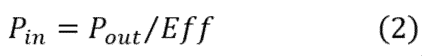
次に、温度推定回路110_7は、インバータ出力電力Pout、入力電力Pinからインバータ102の損失ILOSSを算出する。インバータ102の損失ILOSSを算出する演算式は、下記式(3)で示される。
Next, the temperature estimation circuit 110_7 calculates the loss ILOSS of the


なお、本実施の形態の演算では、インバータ102の損失ILOSSがパワー半導体素子102a~102fの総損失SLOSSと一致するものとして計算しているが、フィルムコンデンサ、バスバー、放電抵抗など、インバータを構成する他の部品の損失を考慮に含めることもできる。この場合、インバータ102の損失ILOSSから、他の部品の損失を差し引いたものを、パワー半導体素子102a~102fの総損失SLOSSとすればよい。
In the calculation of the present embodiment, the loss ILOSS of the
また、本実施の形態の演算では、パワー半導体素子102a~102fの熱抵抗を等しくRthとしているが、パワー半導体素子102a~102fの個別の熱抵抗Rtha~Rthfを事前に取得することで、パワー半導体素子102a~102fを駆動システム100へ実装する条件に起因するパワー半導体素子102a~102fの熱抵抗の違いを考慮した演算を行うこともできる。個別の熱抵抗Rtha~Rthfを用いてパワー半導体素子102a~102fの温度TSa~TSfを算出する場合は、下記式(7)で示される計算式を使用する。
Further, in the calculation of the present embodiment, the thermal resistances of the

温度推定回路110_7は、演算によって求めたパワー半導体素子102a~102fの温度TS(TSa,TSb,TSc,TSd,TSe,TSf)を、保護回路110_8に出力する。
The temperature estimation circuit 110_7 outputs the temperature TS (TSa, TSb, TSc, TSd, TSe, TSf) of the
保護回路110_8は、パワー半導体素子102a~102fの温度TSa~TSfを入力し、いずれかのパワー半導体素子が過熱状態にあると判断した場合、過熱状態にあるパワー半導体素子の駆動を停止させ、すみやかに通常状態(非過熱状態)に復帰するように、制御装置103を制御する。以下に、その制御方法を実現するための具体的な構成例を述べる。
The protection circuit 110_8 inputs the temperatures TSa to TSf of the
本実施の形態では、保護回路110_8は過熱温度閾値Tthを保持する。過熱温度閾値Tthは、パワー半導体素子が過熱状態であると判断する基準温度を示すものであり、例えば80℃に設定される。保護回路110_8は、パワー半導体素子102a~102fの温度TSa~TSfの各々と過熱温度閾値Tthとを比較する。TSa~TSfのいずれかがTthを上回った場合、保護回路110_8はトルク指示値決定回路110_1に対して、インバータ102が過熱状態であることを示す異常信号ABNを出力する。トルク指示値決定回路110_1は、異常信号ABNを受け付けた場合、モータ101の駆動を停止させるため、トルク指示値TQSとして零値を出力する。具体的には、トルクマップ110_5を参照して、TQS=0[Nm]の電流指示値Ids=0[A]、Iqs=0[A]を出力する。この結果、すべてのパワー半導体素子102a~102fに電流は流れず、過熱状態にあるパワー半導体素子は冷却される。
In this embodiment, the protection circuit 110_8 holds the superheat temperature threshold Tth. The superheat temperature threshold value Tth indicates a reference temperature for determining that the power semiconductor element is in a superheated state, and is set to, for example, 80 ° C. The protection circuit 110_8 compares each of the temperatures TSa to TSf of the
本実施の形態にかかる駆動システム100の動作フローの一例を、図6を参照しながら説明する。まず、アクセル指示値Asに対応したトルク指示値TQSを算出する(ステップS101)。次に、算出されたトルク指示値TQSを使用して、d軸電流指示値Ids、q軸電流指示値Iqs、インバータ効率値Eff、d軸電圧指示値Vdsおよびq軸電圧指示値Vqsを算出する(ステップS102)。次に、d軸電圧指示値Vdsおよびq軸電圧指示値Vqsに基づいて、6つのパワー半導体素子102a~102fを駆動するためのDuty比PWMH_D(Hu_D,Hv_D,Hw_D)およびPWML_D(Lu_D,Lv_D,Lw_D)を算出する(ステップS103)。次に、Duty比PWMH_DとPWML_Dに基づいて3相電圧信号PWMH(Hu,Hv,Hw)およびPWML(Lu,Lv,Lw)を生成し、パワー半導体素子102a~102fのゲートを駆動することによりインバータ102を動作させ、モータ101を駆動する(ステップS104)。次に、d軸電流指示値Ids、q軸電流指示値Iqs、インバータ効率値Eff、d軸電圧指示値Vdsおよびq軸電圧指示値Vqsに基づいて、パワー半導体素子102a~102fの総損失SLOSSを算出する(ステップS105)。そして、総損失SLOSS、Duty比PWMH_D、PWML_D、熱抵抗Rthおよび温度計測値TPに基づいて、パワー半導体素子102a~102fの温度TSa~TSfを算出する(ステップS106)。
An example of the operation flow of the
本実施の形態にかかる電子制御回路110の動作例を、駆動システム100の動作例と関連付けながら図7を用いて説明する。図7は、実施の形態1にかかる電子制御回路110の動作の一例を模式的に示すタイミングチャートである。まず状態(1)でアクセル106が押下され、駆動システム100はトルクTQ1でモータ101を駆動しない状態から、トルクTQ2でモータ101を駆動する加速状態となる。モータの駆動中、水温TPおよびパワー半導体素子102aの温度TSaは上昇する。次に、状態(2)でアクセル106の押下量が減少し、駆動システム100は減少されたトルクTQ3に基づきモータ101を駆動する巡行状態となる。水温TPおよびパワー半導体素子102aの温度TSaは状態(2)の直前に比較すると低下するものの、モータ101の駆動は続いているため緩やかに上昇を続ける。続いて状態(3)および状態(4)は、それぞれ状態(1)および状態(2)と同様のトルク指示値TQ2、TQ3でモータ101が駆動されるが、状態(2)によって直前までモータ101の駆動を継続していたため、水温TPおよびパワー半導体素子102aの温度TSaは上昇している。続いて、状態(5)で再びアクセル106が押下され、駆動システム100はトルクTQ2でモータ101を駆動する加速状態となり、水温TPおよびパワー半導体素子102aの温度TSaはさらに上昇を始める。次に、状態(6)で、保護回路110_8が、パワー半導体素子102aの温度TSaが過熱温度閾値Tthを上回ったことを検出し、異常信号ABNを出力する。異常信号ABNを受け付けたトルク指示値決定回路110_1はトルク指示値をTQ1とし、駆動システム100はトルクTQ1でモータ101を駆動しない状態となる。これによって、パワー半導体素子102aの温度TSaが過熱温度閾値Tthに達した時にモータ101の駆動が停止され、過熱状態にあるパワー半導体素子102aを冷却することができる。
An operation example of the
本実施の形態の主な効果は以下の通りである。本実施の形態にかかる駆動システム100は、温度推定回路110_7を有する。温度推定回路110_7は、トルク指示値TQSに対応するインバータの効率値Effを取得し、この効率値Effをもとにインバータ全体の損失ILOSSを算出する。続いて、温度推定回路110_7は、各パワー半導体素子を駆動するDuty比PWMH_DとPWML_Dに基づいて、インバータ102を構成するパワー半導体素子102a~102fのそれぞれに対して、インバータ全体の損失ILOSSの内訳を分配する演算を行うことで、パワー半導体素子102a~102fそれぞれの損失SLOSSa~SLOSSfを得る。そして、温度推定回路110_7は、各パワー半導体素子の損失と既知の熱抵抗値に基づく演算により、パワー半導体素子の温度TSa~TSfを算出する。
The main effects of this embodiment are as follows. The
このような構成により、インバータ102の電力効率値Effに基づいて、各パワー半導体素子の損失SLOSSa~SLOSSfを算出することにより、各パワー半導体素子102a~102fの温度TSa~TSfを高速かつ精度良く推定することができる。
With such a configuration, the temperatures TSa to TSf of each
そして、いずれかのパワー半導体素子の温度が過熱状態であると判断した場合、保護回路110_8の働きによってモータ101の駆動が停止され、過熱状態にあるパワー半導体素子が冷却されるため、駆動システム100は、故障や発火を防止することができる。
When it is determined that the temperature of any of the power semiconductor elements is in an overheated state, the protection circuit 110_8 stops driving the
なお、自律運転システムが備えられた車両の場合は、アクセルペダル106の状態によらず、自立運転システムがアクセル指示値Asやトルク指示値TQSを生成し、制御装置103に出力することもできる。
In the case of a vehicle equipped with an autonomous driving system, the self-sustaining driving system can generate an accelerator instruction value As and a torque instruction value TQS and output them to the
(トルクマップの構成例)
図8に、回転数REV=950[rpm]、モータ駆動電圧VBUS=300[V]の条件におけるトルクマップを示す。トルクマップには、トルク(Torque)に対応するd軸電流Id、q軸電流Iqおよび効率(Efficiency)が記録されている。例としてトルク指示値TQSが54.0[Nm]である場合、対応するd軸電流指示値Ids=-29.62[A]、q軸電流指示値Iqs=81.38[A]、そしてインバータの効率値Eff=93.6[%]である。
(Torque map configuration example)
FIG. 8 shows a torque map under the conditions of rotation speed REV = 950 [rpm] and motor drive voltage VBUS = 300 [V]. In the torque map, the d-axis current Id, the q-axis current Iq, and the efficiency corresponding to the torque (Torque) are recorded. As an example, when the torque indicated value TQS is 54.0 [Nm], the corresponding d-axis current indicated value I ds = -29.62 [A], the q-axis current indicated value I qs = 81.38 [A], The efficiency value of the inverter is Eff = 93.6 [%].
半導体メモリ110_6には、他の回転数REVとモータ駆動電圧VBUSの組み合わせに対応して、複数のパターンのトルクマップ110_5が保存されている。回転数REVとモータ駆動電圧VBUSが変わると、トルクマップ110_5は適宜対応するものに変更される。 In the semiconductor memory 110_6, a plurality of patterns of torque maps 110_5 are stored corresponding to the combination of the other rotation speed REV and the motor drive voltage VBUS. When the rotation speed REV and the motor drive voltage VBUS change, the torque map 110_5 is changed to the corresponding one as appropriate.
ベクトル指示回路110_2は、回転数REVとモータ駆動電圧VBUSが複数のトルクマップ110_5中のいずれにも該当しない場合、複数のパターンのトルクマップ110_5の中に存在する値から最も近い値を採用することができる。また、線形補間や多項式補間等の補間方法を用いることによって、対応するトルク指示値、d軸電流指示値Ids、q軸電流指示値Iqs、インバータ効率値Effを算出することもできる。 When the rotation speed REV and the motor drive voltage VBUS do not correspond to any of the plurality of torque maps 110_5, the vector indicating circuit 110_2 adopts the value closest to the value existing in the torque maps 110_5 of the plurality of patterns. Can be done. Further, by using an interpolation method such as linear interpolation or polynomial interpolation, the corresponding torque indicated value, d-axis current indicated value Ids, q-axis current indicated value Iqs, and inverter efficiency value Eff can be calculated.
ベクトル指示回路110_2は、トルク指示値決定回路110_1から入力したトルク指示値TQSとトルクマップ110_5を用いて、所望のトルクをモータ101が出力するためにモータ101に流すべき電流値として、d軸電流指示値Ids、q軸電流指示値Iqsを出力する。
The vector indicator circuit 110_2 uses the torque indicator value TQS input from the torque indicator value determination circuit 110_1 and the torque map 110_5 as a d-axis current as a current value to be passed through the
トルク指示値TQSがトルクマップ110_5中に存在しない数値の場合、ベクトル指示回路110_2は、トルクマップ110_5中に存在する値に基づいて最も近い値を採用することができる。その他の手法として、線形補間や多項式補間等の補間方法を用いることによって、トルク指示値に対応するd軸電流指示値Ids、q軸電流指示値Iqsおよびインバータの効率値Effを算出することもできる。 When the torque indicated value TQS is a numerical value that does not exist in the torque map 110_5, the vector indicating circuit 110_2 can adopt the closest value based on the value existing in the torque map 110_5. As another method, by using interpolation methods such as linear interpolation and polynomial interpolation, the d-axis current indicated value I ds , the q-axis current indicated value I qs , and the efficiency value Eff of the inverter corresponding to the torque indicated value are calculated. You can also.
また、本実施の形態にかかる駆動システム100は、モータ101を力行させる場合、すなわちトルク指示値TQSが正の場合だけではなく、モータ101を回生させる場合、すなわちトルク指示値TQSが負の場合にも、パワー半導体素子102a~102fの温度TSa~TSfを推定することができる。
Further, the
(ゲート駆動回路111の構成例)
図9は、実施の形態1にかかるゲート駆動回路111の構成例である。ゲート駆動回路111は、電子制御回路110と、インバータ102の間に設けられる。ゲート駆動回路111は、インバータ102と制御装置103とを電気的に絶縁しながら、磁気結合により信号の送受信を行うアイソレータ111_1a~111_1fと、パワー半導体装置102a~102fのゲートを駆動するプリドライバ111_2a~111_2fを含む。
(Configuration example of gate drive circuit 111)
FIG. 9 is a configuration example of the
プリドライバ111_2a~111_2fは、相補の3相電圧信号PWMH(Hu,Hv,Hw)、PWML(Lu,Lv,Lw)に基づいて、対応するパワー半導体素子(102a、102c、102e)および(102b、102d、102f)のゲートをそれぞれ制御するためのゲート駆動信号DPWMH(DHu,DHv,DHw)およびDPWML(DLu,DLv,DLw)を出力する。 The pre-drivers 111_2a to 111_2f are based on complementary three-phase voltage signals PWMH (Hu, Hv, Hw), PWML (Lu, Lv, Lw) and corresponding power semiconductor devices (102a, 102c, 102e) and (102b, The gate drive signals DPWMH (DHu, DHv, DHw) and DCTL (DLu, DLv, DLw) for controlling the gates of 102d and 102f) are output.
ゲート駆動回路111は、MCU等の低電圧デバイスで構成された電子制御回路110と、パワーデバイスで構成されたインバータ102を絶縁する役割を有することから、電子制御回路110やインバータ102とは独立した半導体装置で構成することが望ましい。本実施の形態1にかかるゲート駆動回路111では、アイソレータ111_1a~111_1fとプリドライバ111_2a~111_2fは、それぞれ1対になって各々1つの駆動用半導体装置111_3a~111_3f内に搭載されている。
Since the
(パワー半導体素子102a~102fの構成例)
図10に、パワー半導体素子102aの構成例を示す。パワー半導体102b~102fも、図10に示すパワー半導体素子102aと同様の構成である。パワー半導体102aは、絶縁ゲートバイポーラトランジスタ(IGBT)102a_1とファストリカバリーダイオード(FRD)102a_2を含む。IGBT102a_1に電流が流れている時は、IGBT102a_1が発熱する。また、FRD102a_2に電流が流れている時は、FRD102a_2が発熱する。
(Structure example of
FIG. 10 shows a configuration example of the
すなわち、IGBT102a_1の発熱が電圧信号Huのデューティ比Hu_Dに依存するのに対し、FRD102a_2の発熱は電圧信号Huの(1-Hu_D)に依存する。従って、温度の推定にデューティ比Hu_Dを使用することに代えて(1-Hu_D)を使用することにより、FRD102a_2の損失SLOSS_FRDを推定することができる。加えてFRD102a_2の熱抵抗Rth_FRDが既知であれば、FRD102a_2のジャンクション温度TSa_FRDも推定することもできる。以上のFRD102_aの温度推定方法をパワー半導体102b~102fのFRD102b_2~102f_2にも適用することにより、6つのFRD102a_2~102f_2の温度TS_FRD(TSa_FRD,TSb_FRD,TSc_FRD,TSd_FRD,TSe_FRD,TSf_FRD)を推定することができる。
That is, the heat generation of the IGBT 102a_1 depends on the duty ratio Hu_D of the voltage signal Hu, whereas the heat generation of the FRD102a_1 depends on (1-Hu_D) of the voltage signal Hu. Therefore, by using (1-Hu_D) instead of using the duty ratio Hu_D for temperature estimation, the loss SLOSS_FRD of FRD102a_2 can be estimated. In addition, if the thermal resistance Rth_FRD of FRD102a_2 is known, the junction temperature TSa_FRD of FRD102a_2 can also be estimated. By applying the above temperature estimation method of FRD102_a to FRD102b_2 to 102f_2 of
(実施の形態1の変形例)
図11は、実施の形態1にかかる電子制御回路110の変形例における、温度試算モードの構成例である。これに比較すると、図5の電子制御回路110は通常動作モードの構成例である。すなわち、電子制御回路110の機能はプロセッサを用いるプログラムにより実装されるため、動作モードの変更に応じて、構成要素やその接続関係を変更することができる。
(Modified Example of Embodiment 1)
FIG. 11 is a configuration example of the temperature trial calculation mode in the modified example of the
本変形例では、パワー半導体素子102a~102fの温度TSa~TSfのいずれかが過熱温度閾値Tthを上回った場合、電子制御回路110は一時的に、図11に示す温度試算モードの構成となる。図11の構成の電子制御回路110では、ベクトル指示回路110_2はトルク指示値TQSではなく、仮想トルク指示回路110_9が生成した仮想トルク値TQSVを入力する。仮想トルク値TQSVは、インバータ102を駆動している信号には関係しない。
In this modification, when any of the temperatures TSa to TSf of the
電子制御回路110は、仮想トルク値TQSVでインバータ102が駆動されると仮定し、実施の形態1と同様の方法により、温度推定回路110_7によってパワー半導体素子102a~102fの仮想温度TSV(TSVa,TSVb,TSVc,TSVd,TSVe,TSVf)を推定する。一方で、仮想トルク値TQSVに基づいて生成された信号はゲート駆動回路111には出力しない。
The
電子制御回路110は、例えば仮想トルク値TQSVとしてトルク指示値TQSの2分の1の値を設定し、仮想温度TSVa~TSVfが過熱温度閾値Tthを上回らない場合、仮想トルク値TQSVを、過熱を避ける動作範囲内で許容可能なトルクとしてトルク指示値決定回路110_1に伝達する。トルク指示値決定回路110_1は、アクセル指示値Asに基づかず、仮想トルク指示値TQSVの値をトルク指示値TQSとして採用する。その後、電子制御回路110は通常モード(図5)に戻り、実施の形態1に説明した駆動制御を行う。
For example, the
もし仮想トルク値TQSVとしてトルク指示値TQSの2分の1の値を使用しても仮想温度TSVa~TSVfが過熱温度閾値Tthを上回る場合、仮想トルク値TQSVを、トルク指示値TQSの3分の1の値、4分の1の値と漸減させ、それらに基づく仮想温度TSVa~TSVfを順次算出する。そして、過熱温度閾値Tthを上回らない仮想温度TSVa~TSVfが得られた時点の仮想トルク値TQSVを、トルク指示値TQSの値として採用する。 If the virtual temperature TSVa to TSVf exceeds the superheat temperature threshold Tth even if a half of the torque indicated value TQS is used as the virtual torque value TQSV, the virtual torque value TQSV is used as a third of the torque indicated value TQS. The value is gradually reduced to a value of 1 and a value of 1/4, and the virtual temperatures TSVa to TSVf based on them are sequentially calculated. Then, the virtual torque value TQSV at the time when the virtual temperatures TSVa to TSVf that do not exceed the superheat temperature threshold Tth are obtained is adopted as the value of the torque indicated value TQS.
本変形例に特有の効果は以下の通りである。すなわち、電子制御回路110は、パワー半導体素子102a~102fの温度TSa~TSfのいずれかが過熱温度閾値Tthを上回った場合でも、過熱を防ぎながらインバータ102の駆動を維持し、車両が走行を継続できるように制御を行うことができる。
The effects peculiar to this modification are as follows. That is, even if any of the temperatures TSa to TSf of the
[実施の形態2]
続いて、実施の形態2について説明する。実施の形態2では、実施の形態1にかかる電子制御回路110の別の形態となる電子制御回路110aについて説明する。図12は、実施の形態2にかかる電子制御回路110aの構成の一例を示す図である。実施の形態2において、電子制御回路110a以外の構成は、実施の形態1と同様でよい。また、電子制御回路110aの内部の構成は、実施の形態1と同じ符号が付されているものに関する説明は、実施の形態1の説明を準用する。
[Embodiment 2]
Subsequently, the second embodiment will be described. In the second embodiment, the
図12に示すように、実施の形態2にかかる電子制御回路110aは、実施の形態1にかかる電子制御回路110と比較して、トルク管理回路110_10、信号生成・温度推定回路110_11、仮想ベクトル指示回路110_12、温度管理回路110_13が追加されている。また、トルク指示値決定回路110_1、制御信号生成回路110_4、温度推定回路110_7、保護回路110_8は除かれている。
As shown in FIG. 12, the
トルク管理回路110_10は、アクセル指示値Asに基づき、モータ101が出力すべきトルクを指示するトルク指示値TQSを算出し、ベクトル指示回路110_2に出力する。
The torque management circuit 110_10 calculates a torque instruction value TQS that indicates the torque to be output by the
また、トルク管理回路110_10は、インバータ102を任意のトルクで駆動することを仮定し、仮想トルク値TQS_vtを算出し、仮想ベクトル指示回路110_12に出力する。
Further, the torque management circuit 110_10 calculates the virtual torque value TQS_vt on the assumption that the
ベクトル指示回路110_2は、トルク指示値決定回路110_1から入力したトルク指示値TQSに基いて、d軸電流指示値Ids、q軸電流指示値Iqs、これらの電流条件でモータ101を駆動した場合のインバータ効率値Effを、信号生成・温度推定回路110_11に出力する。
When the vector instruction circuit 110_2 drives the
仮想ベクトル指示回路110_2は、トルク指示値決定回路110_1から入力した仮想トルク指示値TQS_vtに基いて、仮想d軸電流指示値Ids_vt、仮想q軸電流指示値Iqs_vt、これらの電流条件でモータ101を駆動した場合の仮想インバータ効率値Eff_vtを、信号生成・温度推定回路110_11に出力する。
The virtual vector instruction circuit 110_2 is based on the virtual torque instruction value TQS_vt input from the torque instruction value determination circuit 110_1, and has a virtual d-axis current instruction value I ds _vt and a virtual q-axis current instruction value I qs _vt under these current conditions. The virtual inverter efficiency value Eff_vt when the
信号生成・温度推定回路110_11は、実施の形態1にかかる制御信号生成回路110_4と温度推定回路110_7の機能を包含する。すなわち、実施の形態1と同様の方法により、d軸電流測定値Idmとq軸電流測定値Iqm、および、d軸電流指示値Idsとq軸電流指示値Iqsに基づいて、相補の3相電圧信号PWMH(Hu,Hv,Hw)およびPWML(Lu,Lv,Lw)を生成する。さらに、相補の3相電圧信号の各々のDuty比PWMH_D(Hu_D,Hv_D,Hw_D)、PWML_D(Lu_D,Lv_D,Lw_D)、d軸電流指示値Ids、q軸電流指示値Iqs、d軸電圧指示値Vds、q軸電圧指示値Vqs、温度計測値TPおよびインバータ効率値Effに基づいて、パワー半導体素子102a~102fの温度TS(TSa,TSb,TSc,TSd,TSe,TSf)を推定する。
The signal generation / temperature estimation circuit 110_11 includes the functions of the control signal generation circuit 110_4 and the temperature estimation circuit 110_7 according to the first embodiment. That is, by the same method as in the first embodiment, the d-axis current measured value I dm and the q-axis current measured value I qm are complemented based on the d-axis current indicated value I ds and the q-axis current indicated value I qs . 3 phase voltage signals PWMH (Hu, Hv, Hw) and PWML (Lu, Lv, Lw) are generated. Further, each Duty ratio PWMH_D (Hu_D, Hv_D, Hw_D), PWML_D (Lu_D, Lv_D, Lw_D), d-axis current indicated value I ds , q-axis current indicated value I qs , d-axis voltage of each of the complementary three-phase voltage signals. Estimate the temperature TS (TSa, TSb, TSc, TSd, TSe, TSf) of the
また、信号生成・温度推定回路110_11は、d軸電流測定値Idm、q軸電流測定値Iqm、仮想d軸電流指示値Ids_vt、仮想q軸電流指示値Iqs_vt、温度計測値TPおよび仮想インバータ効率値Eff_vtに基づいて、パワー半導体素子102a~102fの仮想温度TS_vt(TSa_vt,TSb_vt,TSc_vt,TSd_vt,TSe_vt,TSf_vt)を推定する。
Further, the signal generation / temperature estimation circuit 110_11 has a d-axis current measured value I dm , a q-axis current measured value I qm , a virtual d-axis current indicated value I ds _vt, a virtual q-axis current indicated value I qs _vt, and a temperature measured value. Based on the TP and the virtual inverter efficiency value Eff_vt, the virtual temperature TS_vt (TSa_vt, TSb_vt, TSc_vt, TSd_vt, TSe_vt, TSf_vt) of the
温度管理回路110_13は、実施の形態1にかかる保護回路110_8の機能を包含する。すなわち、温度管理回路110_13は過熱温度閾値Tthを保持し、TSa~TSfのいずれかがTthを上回った場合、トルク管理回路110_10に対して、インバータ102が過熱状態であることを示す異常信号ABNを出力する。トルク管理回路110_10は、異常信号ABNを受け付けた場合、モータ101の駆動を停止させるため、トルク指示値TQSとして零値を出力する。具体的には、トルクマップ110_5を参照して、TQS=0[Nm]の電流指示値Ids=0[A]、Iqs=0[A]を出力する。この結果、すべてのパワー半導体素子102a~102fに電流は流れず、過熱状態にあるパワー半導体素子は冷却される。
The temperature control circuit 110_13 includes the function of the protection circuit 110_8 according to the first embodiment. That is, the temperature control circuit 110_13 holds the superheat temperature threshold value Tth, and when any of TSa to TSf exceeds Tth, an abnormal signal ABN indicating that the
さらに、温度管理回路110_13はTSa_vt~TSf_vtのいずれかがTthを上回った場合、トルク管理回路110_10に対して、仮想トルク指示値TQS_vtでモータ101を駆動すると仮定した場合、インバータ102が過熱状態になることを示す仮想異常信号ABN_vtを出力する。トルク管理回路110_10は、異常信号ABN_vtを受け付けた場合、トルク指示値TQSとして仮想トルク指示値TQS_vtを超える値を出力しないよう、トルク管理回路110_10を制御する。
Further, when any of TSa_vt to TSf_vt exceeds Tth in the temperature control circuit 110_13, the
具体的には、トルク管理回路110_10は制限回路110_10_1(図示せず)を備える。制限回路110_10_1は、トルク指示値TQSとトルク制限値TQS_limitとを比較し、トルク指示値TQSがトルク制限値TQS_limitを上回る場合、トルク指示値TQSとしてトルク制限値TQS_limitを出力する。トルク制限値TQS_limitとして仮想トルク指示値TQS_vtを設定した場合、アクセル指示値Asの値によらず、トルク管理回路110_10は、仮想トルク指示値TQS_vtを上回るトルク指示値TQSを出力することはない。 Specifically, the torque management circuit 110_10 includes a limiting circuit 110_10_1 (not shown). The limiting circuit 110_10_1 compares the torque indicated value TQS with the torque limit value TQS_limit, and when the torque indicated value TQS exceeds the torque limit value TQS_limit, outputs the torque limit value TQS_limit as the torque indicated value TQS. When the virtual torque instruction value TQS_vt is set as the torque limit value TQS_limit, the torque management circuit 110_10 does not output the torque instruction value TQS exceeding the virtual torque instruction value TQS_vt regardless of the value of the accelerator instruction value As.
トルク管理回路110_10は、任意の仮想トルク指示値TQS_vtを出力したことに対応して仮想異常信号ABN_vtを受け取った場合、仮想トルク指示値TQS_vtを漸減させながら順次出力する。そして、仮想異常信号ABN_vtが出力されなくなった時点の仮想トルク指示値TQS_vtを、トルク制限値TQS_limitとして採用する。 When the torque management circuit 110_10 receives the virtual abnormality signal ABN_vt in response to the output of an arbitrary virtual torque instruction value TQS_vt, the torque management circuit 110_10 sequentially outputs the virtual torque instruction value TQS_vt while gradually reducing it. Then, the virtual torque instruction value TQS_vt at the time when the virtual abnormality signal ABN_vt is no longer output is adopted as the torque limit value TQS_limit.
また、トルク管理回路110_10は、任意の仮想トルク指示値TQS_vtを出力したことに対して仮想異常信号ABN_vtを受け取らなかった場合、仮想トルク指示値TQS_vtを漸増させながら順次出力する。そして、仮想異常信号ABN_vtが出力された時点の仮想トルク指示値TQS_vtを、トルク制限値TQS_limitとして採用する。 Further, when the torque management circuit 110_10 does not receive the virtual abnormality signal ABN_vt in response to the output of an arbitrary virtual torque instruction value TQS_vt, the torque management circuit 110_10 sequentially outputs the virtual torque instruction value TQS_vt while gradually increasing it. Then, the virtual torque instruction value TQS_vt at the time when the virtual abnormality signal ABN_vt is output is adopted as the torque limit value TQS_limit.
加えて、信号生成・温度推定回路110_11は、インバータ101が過熱状態とならない許容インバータ損失ILOSS_maxを算出する機能を有する。許容インバータ損失ILOSS_maxを算出する演算式は、下記式(8)で示される。
In addition, the signal generation / temperature estimation circuit 110_11 has a function of calculating the allowable inverter loss ILOSS_max in which the

本実施の形態の主な効果は以下の通りである。電子制御回路110aは、インバータ102を駆動している条件におけるパワー半導体素子102a~102fの温度TS(TSa,TSb,TSc,TSd,TSe,TSf)を推定しながら、仮想の駆動条件におけるパワー半導体素子102a~102fの仮想温度TS_vt(TSa_vt,TSb_vt,TSc_vt,TSd_vt,TSe_vt,TSf_vt)を推定することができる。また、インバータ102が過熱状態とならない最大の許容インバータ損失ILOSS_maxを算出し、トルク管理回路110_10に通知し、トルク管理回路110_10において出力トルクの制限を行うことができる。
The main effects of this embodiment are as follows. The
なお、トルク管理回路110_10における出力トルクの制限は、車両や駆動システム100における他の条件および要素と組み合わせて実施することができる。たとえば、トルク制限値TQS_limitは、バッテリ108の残量に応じて設定されることもできる。
The limitation of the output torque in the torque management circuit 110_10 can be implemented in combination with other conditions and elements in the vehicle and the
[実施の形態3]
続いて、実施の形態3について説明する。実施の形態3では、実施の形態1にかかる電子制御回路110の別の形態となる電子制御回路110bについて説明する。図13は、実施の形態3にかかる電子制御装置110bの構成の一例を示す図である。実施の形態3において、電子制御回路110b以外の構成は、実施の形態1と同様でよい。また、電子制御回路110bの内部の構成は、実施の形態1と同じ符号が付されているものに関する説明は、実施の形態1の説明を準用する。
[Embodiment 3]
Subsequently, the third embodiment will be described. In the third embodiment, the
図13に示すように、実施の形態3にかかる電子制御回路110bは、実施の形態1にかかる電子制御回路110と比較して、温度推定回路110_7に替えて温度推定回路110_7b、保護回路110_8に替えて保護回路110_8bが含まれる。
As shown in FIG. 13, the
本実施例にかかる温度推定回路110_7bは、トルク指示値TQSでモータ101を駆動してから任意の時間経過後のパワー半導体素子102a~102fの温度を推定する機能を有する。温度推定回路110_7bは、温度の推定基準となる経過時間Elapを保護回路110_8bから入力する。そして、経過時間Elapが経過したときのパワー半導体素子102a~102fの温度TS_elap(TSa_elap,TSb_elap,TSc_elap,TSd_elap,TSe_elap,TSf_elap)を推定し、保護回路110_8bへ出力する。以下に、その温度推定を実現するための具体的な構成例を述べる。
The temperature estimation circuit 110_7b according to this embodiment has a function of estimating the temperature of the
保護回路110_8bは、トルクTQSでモータ101を駆動し続けてから経過時間Elapだけ経過した際のパワー半導体素子102a~102fの温度推測値TSa_elap~TSf_elapを得るため、温度推定回路110_7bに経過時間Elapを出力する。
The protection circuit 110_8b applies an elapsed time Elap to the temperature estimation circuit 110_7b in order to obtain temperature estimation values TSa_elap to TSf_elap of the
実施の形態1にかかる温度推定回路110_7が温度推定に熱抵抗Rthを使用するのに対して、実施の形態3にかかる温度推定回路110_7bは温度推定に過渡熱抵抗Rth_tranを使用する。過渡熱抵抗Rth_tranとは発熱時間に伴う熱抵抗の変化のことであり、本実施の形態では、パワー半導体素子102a~102fのジャンクション(接合)部の温度を算出するための過渡熱抵抗を等しくRth_tranとする。
The temperature estimation circuit 110_7 according to the first embodiment uses the thermal resistance Rth for temperature estimation, whereas the temperature estimation circuit 110_7b according to the third embodiment uses the transient thermal resistance Rth_tran for temperature estimation. The transient thermal resistance Rth_tran is a change in thermal resistance with heat generation time, and in the present embodiment, the transient thermal resistance for calculating the temperature of the junction (junction) of the
図14に、過渡熱抵抗Rth_tranの例を示す。横軸は発熱時間[s]、縦軸は熱抵抗[℃/W]である。ここで、経過時間Elapにおける熱抵抗をRth_tran(Elap)と記載すれば、発熱が1秒続いた際、すなわちElap=1(1.0E+00)における熱抵抗Rth_tran(Elap)は約0.15[℃/W]であり、発熱が10秒続いた際、すなわちElap=10(1.0E+0.1)における熱抵抗Rth_tran(Elap)は約0.22[℃/W]である。 FIG. 14 shows an example of the transient thermal resistance Rth_tran. The horizontal axis is the heat generation time [s], and the vertical axis is the thermal resistance [° C./W]. Here, if the thermal resistance in the elapsed time Elap is described as Rth_tran (Elap), the thermal resistance Rth_tran (Elap) at the time when heat generation continues for 1 second, that is, at Elap = 1 (1.0E + 00) is about 0.15 [° C. / W], and the thermal resistance Rth_tran (Elap) is about 0.22 [° C./W] when the heat generation continues for 10 seconds, that is, at Elap = 10 (1.0E + 0.1).
温度推定回路110_7bは、入力した経過時間Elapに基づいて、トルク指示値TQSでモータ101が駆動され続けて経過時間Elapが経過した際の熱抵抗Rth_tran(Elap)を算出する。
The temperature estimation circuit 110_7b calculates the thermal resistance Rth_tran (Elap) when the
温度推定回路110_7は、下記式(9)で示される計算式によって、トルク指示値TQSでモータ101を駆動して経過時間Elapだけ経過した時点の、パワー半導体素子102a~102fの温度TS_elap(TSa_elap,TSb_elap,TSc_elap,TSd_elap,TSe_elap,TSf_elap)を求める。
The temperature estimation circuit 110_7 uses the calculation formula shown by the following formula (9) to drive the
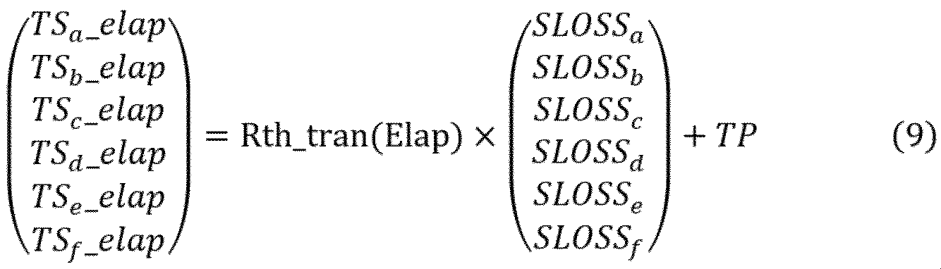
また、本実施の形態の演算では、パワー半導体素子102a~102fの過渡熱抵抗を等しくRth_tranとしているが、パワー半導体素子102a~102fの個別の過渡熱抵抗Rtha_tran~Rthf_tranを事前に取得することで、パワー半導体素子102a~102fを駆動システム100へ実装する条件に起因するパワー半導体素子102a~102fの過渡熱抵抗の違いを考慮した演算を行うこともできる。個別の熱抵抗Rtha_tran~Rthf_tranを用いて、経過時間Elapが経過した際のパワー半導体素子102a~102fの温度TSa_elap~TSf_elapを算出する場合は、下記式(10)で示される演算式を使用する。
Further, in the calculation of the present embodiment, the transient thermal resistances of the

本実施の形態にかかる電子制御回路110bの動作例を、駆動システム100の動作例と関連付けながら図15を用いて説明する。図15は、実施の形態3にかかる電子制御回路110bの動作の一例を模式的に示すタイミングチャートである。状態(1)から状態(5)までの説明は、実施の形態1に関連する図7の説明と同一とする。次に、状態(6)で、保護回路110_8bが、経過時間Elapが経過した際のパワー半導体素子102aの温度TSa_elapが過熱温度閾値Tthを上回ることを検出し、異常信号ABN_elapを出力する。異常信号ABN_elapを受け付けたトルク指示値決定回路110_1は、出力トルクを制限する制御により、トルク指示値をTQ2からTQ4に切り替える。これによって、パワー半導体素子102aの温度TSaが過熱温度閾値Tthに達する前に、パワー半導体素子102aの過熱を防ぐことができる。
An operation example of the
本実施の形態の主な効果は以下の通りである。本実施の形態にかかる駆動システム100は、温度推定にパワー半導体素子の過渡熱抵抗Rth_tranを使用することによって、トルクTQSでモータ101を駆動し続けてから経過時間Elapだけ経過した際の、パワー半導体素子102a~102fの温度TSa_elap~TSf_elapを推測することができる。
The main effects of this embodiment are as follows. The
かかる構成によれば、未来の予測に基づいた制御を行うことができるため、インバータ102が過熱状態に至る前に保護動作を行うことができる。従って、駆動システム100は、任意の安全マージンに基づいて、故障や発火の防止制御を行うことができる。
According to such a configuration, since the control can be performed based on the prediction of the future, the protection operation can be performed before the
以上、本発明者によってなされた発明を実施の形態に基づき具体的に説明したが、本発明は既に述べた実施の形態に限定されるものではなく、その要旨を逸脱しない範囲において種々の変更が可能であることはいうまでもない。 Although the invention made by the present inventor has been specifically described above based on the embodiments, the present invention is not limited to the embodiments already described, and various changes can be made without departing from the gist thereof. It goes without saying that it is possible.
100 駆動システム
101 モータ
102、1102、2102 インバータ
102a、102b、102c、102d、102e、102f、1102a、1102b、1102c、1102d、1102e、1102f、2102a、2102b、2102c、2102d、2102e、2102f パワー半導体素子
102a_1 IGBT
102a_2 FRD
103、1103、2103 制御装置
104 電流検出器
104u、104v、104w 電流測定器
105、1105a、1105b、1105c、1105d、1105e、1105f 温度センサ
106 アクセルペダル
107 アクセルセンサ
108 バッテリ
109 電気制御系統
110、110a、110b 電子制御回路
110_1 トルク指示値決定回路
110_2 ベクトル指示回路
110_3 電流演算回路
110_4 制御信号生成回路
110_5 トルクマップ
110_6 半導体メモリ
110_7、110_7b 温度推定回路
110_8、110_8b 保護回路
110_9 仮想トルク指示回路
110_10 トルク管理回路
110_11 信号生成・温度推定回路
110_12 仮想ベクトル指示回路
110_13 温度管理回路
111 ゲート駆動回路
111_1a、111_1b、111_1c、111_1d、111_1e、111_1f アイソレータ
111_2a、111_2b、111_2c、111_2d、111_2e、111_2f プリドライバ
111_3a、111_3b、111_3c、111_3d、111_3e、111_3f 駆動用半導体装置
2201 温度モデル演算回路
2202 熱損失モデル回路
2203 熱回路モデル回路
PS 電源
OUT、u、v、w 負荷駆動端子
VBUS、GND 電源電圧
As アクセル指示値
TQS、TQ1、TQ2、TQ3、TQ4 トルク指示値
TQSV、TQS_vt 仮想トルク値
TQS_limit トルク制限値
ISEN、ISENu、ISENv、ISENw、ISEN2 電流測定値
VSEN2 電圧測定値
PWMH、Hu、Hv、Hw、PLWL、Lu、Lv、LW 電圧信号
DPWMH、DHu、DHv、DHw、DPLWL、DLu、DLv、DLw、DPWM1 ゲート駆動信号
TP、TP1、TP2、TP2a、TP2b、TP2c、TP2d、TP2e、TP2f 温度計測値
Ids d軸電流指示値、 Iqs q軸電流指示値
Ids_vt 仮想d軸電流指示値、 Iqs_vt 仮想q軸電流指示値
Idm d軸電流測定値、 Iqm q軸電流指示値
Vds d軸電圧指示値、 Vqs q軸電圧指示値
PWMH_D、Hu_D、Hv_D、Hw_D、PWML_D、Lu_D、Lv_D、Lw_D Duty比
REV モータ回転数
Eff インバータ効率値
Eff_vt 仮想インバータ効率値
TS、TSa、TSb、TSc、TSd、TSe、TSf、TS_elap、TSa_elap、TSb_elap、TSc_elap、TSd_elap、TSe_elap、TSf_elap パワー半導体素子の温度
TSVa、TSVb、TSVc、TSVd、TSVe、TSVf、TS_vt、TSa_vt、TSb_vt、TSc_vt、TSd_vt、TSe_vt、TSf_vt パワー半導体素子の仮想温度
TS_FRD、TSa_FRD、TSb_FRD、TSc_FRD、TSd、FRD、TSe_FRD、TSf_FRD FRDの温度
Pout インバータ出力電力、 Pin インバータ入力電力
ILOSS インバータの損失
ILOSS_max 許容インバータ損失
OLOSS インバータの損失に占めるパワー半導体の損失以外の損失
SLOSS、SLOSSa、SLOSSb、SLOSSc、SLOSSe、SLOSSf パワー半導体素子の損失
SLOSS_FRD FRDの熱抵抗
Ch インバータのチャネル数
Rth、Rtha、Rthb、Rthc、Rthd、Rthe、Rthf 熱抵抗
Rth_tran、Rtha_tran、Rthb_tran、Rthc_tran、Rthd_tran、Rthe_tran、Rthf_tran 過渡熱抵抗」
Tth 過熱温度閾値
ABN、ABN_vt、ABN_ls、ABN_elap 異常信号
Elap 経過時間
100
102a_2 FRD
103, 1103, 2103 Control device 104 Current detector 104u, 104v, 104w Current measuring device 105, 1105a, 1105b, 1105c, 1105d, 1105e, 1105f Temperature sensor 106 Accelerator pedal 107 Accelerator sensor 108 Battery 109 Electric control system 110, 110a, 110b Electronic control circuit 110_1 Torque instruction value determination circuit 110_2 Vector instruction circuit 110_3 Current calculation circuit 110_4 Control signal generation circuit 110_5 Torque map 110_6 Semiconductor memory 110_7, 110_7b Temperature estimation circuit 110_8, 110_8b Protection circuit 110_9 Virtual torque instruction circuit 110_10 Torque management circuit 110_11 Signal generation / temperature estimation circuit 110_12 Virtual vector indicator circuit 110_13 Temperature control circuit 111 Gate drive circuit 111_1a, 111_1b, 111_1c, 111_1d, 111_1e, 111_1f Isolators 111_2a, 111_2b, 111_2c, 111_2d, 111_2e, 111_2f Pre-driver 111_3a, 111_ 111_3d, 111_3e, 111_3f Drive semiconductor device 2201 Temperature model calculation circuit 2202 Heat loss model circuit 2203 Thermal circuit model circuit PS power supply OUT, u, v, w Load drive terminal VBUS, GND Power supply voltage As Accelerator instruction value TQS, TQ1, TQ2 , TQ3, TQ4 Torque indication value TQSV, TQS_vt Virtual torque value TQS_limit Torque limit value IREN, IRENu, IRENv, IRENw, IREN2 Current measured value VSEN2 Voltage measured value PWMH, Hu, Hv, Hw, PLWL, Lu, Lv, LW DPWMH, DHu, DHv, DHw, DPLWL, DLu, DLv, DLw, DPWM1 Gate drive signal TP, TP1, TP2, TP2a, TP2b, TP2c, TP2d, TP2e, TP2f Temperature measurement value I ds d-axis current indicated value, I qs q-axis current indicated value I ds _vt Virtual d-axis current indicated value, I qs _vt Virtual q-axis current indicated value I dm d-axis current measured value, I qm q-axis current indicated value V ds d-axis voltage indicated value, V qs q Shaft voltage indicated values PWMH_D, Hu_D, Hv_D, Hw_D, PWML_D, Lu_D, Lv_D, Lw_D Duty ratio REV Motor rotation speed Eff Inva Data efficiency value Eff_vt Virtual inverter efficiency value TS, TSa, TSb, TSc, TSd, TSe, TSf, TS_elap, TSa_elap, TSb_elap, TSc_elap, TSd_elap, TSe_elap, TSf_elap Power semiconductor device temperature TSVa, TSVb, TSVc Inverter power input Inverter loss ILOSS_max Allowable inverter loss OLOSS Loss other than power semiconductor loss in inverter loss SLOSS, SLOSSa, SLOSSb, SLOSSc, SLOSSe, SLOSSf Power semiconductor element loss SLOSS_FRD FRD thermal resistance Ch Inverter channel number Rth, Rtha, Rthb, Rthc, Rthd, Rthe, Rthf Thermal Resistance Rth_tran, Rthe_tran, Rthb_tran, Rthc_tran, Rthd_tran, Rthe_tran, Rthf_tran Transient Thermal Resistance "
Tth superheat temperature threshold ABN, ABN_vt, ABN_ls, ABN_elap Abnormal signal Elap elapsed time
Claims (20)
前記駆動指示値に対応する効率値を出力する演算回路と、
前記効率値に基づいて、前記電力用半導体素子の温度を推定する温度推定回路と、
を含む制御回路。 A signal generation circuit that generates a drive signal corresponding to a power semiconductor element based on a drive instruction value,
An arithmetic circuit that outputs an efficiency value corresponding to the drive instruction value, and
A temperature estimation circuit that estimates the temperature of the power semiconductor element based on the efficiency value, and
Control circuit including.
前記温度推定回路は、前記効率値と前記第1のデューティ比に基づいて前記推定を行う、
請求項4に記載の制御回路。 The drive signal consists of a PWM signal having a first duty ratio.
The temperature estimation circuit makes the estimation based on the efficiency value and the first duty ratio.
The control circuit according to claim 4.
前記温度推定回路は、前記仮想ベクトル電流値と前記仮想効率値に基づいて、前記電力用半導体素子の仮想温度をさらに推定する、
請求項1に記載の制御回路。 The arithmetic circuit determines a virtual vector current value and a virtual efficiency value corresponding to a virtual drive instruction value that is not output to the power semiconductor element.
The temperature estimation circuit further estimates the virtual temperature of the power semiconductor element based on the virtual vector current value and the virtual efficiency value.
The control circuit according to claim 1.
複数の電力用半導体素子を有し、前記モータを駆動するインバータと、
前記インバータに駆動信号を供給する制御装置と、を有し、
前記制御装置は、
前記モータを駆動するトルクに対応するインバータ駆動値に基づいて前記駆動信号を生成する信号生成回路と、
前記インバータ駆動値に基づいてインバータ効率値を出力する演算回路と、
前記インバータ効率値に基づいて前記複数の電力用半導体素子の温度を推定する温度推定回路と、
を有する駆動システム。 With the motor
An inverter that has multiple power semiconductor elements and drives the motor,
It has a control device that supplies a drive signal to the inverter, and has.
The control device is
A signal generation circuit that generates the drive signal based on the inverter drive value corresponding to the torque that drives the motor, and
An arithmetic circuit that outputs an inverter efficiency value based on the inverter drive value,
A temperature estimation circuit that estimates the temperature of the plurality of power semiconductor elements based on the inverter efficiency value, and
Drive system with.
請求項9に記載の駆動システム。 A holding circuit for holding the inverter drive value and the inverter efficiency value is further included.
The drive system according to claim 9.
前記温度推定回路は、前記温度測定値に基づいて前記複数の電力用半導体素子の温度を推定する、請求項9に記載の駆動システム。 The inverter includes a temperature sensor that outputs a temperature measurement value.
The drive system according to claim 9, wherein the temperature estimation circuit estimates the temperature of the plurality of power semiconductor elements based on the temperature measurement value.
前記温度推定回路は、複数の電力用半導体素子の各々の過渡熱抵抗値に基づいて、前記インバータ駆動値で前記モータを所定の時間駆動した場合の前記複数の電力用半導体素子の各々の温度を推定する、請求項15に記載の駆動システム。 The thermal resistance value consists of a transient thermal resistance value.
The temperature estimation circuit determines the temperature of each of the plurality of power semiconductor elements when the motor is driven for a predetermined time by the inverter drive value based on the transient thermal resistance value of each of the plurality of power semiconductor elements. The drive system according to claim 15, which is estimated.
前記インバータ駆動値に基づいて、インバータを構成する複数の電力用半導体素子を駆動し、
前記インバータ効率値に基づいて、前記複数の電力用半導体素子の温度を推定する、
インバータの制御方法。 Obtain the inverter drive value and inverter efficiency value corresponding to the torque indicated value,
Based on the inverter drive value, a plurality of power semiconductor elements constituting the inverter are driven.
The temperature of the plurality of power semiconductor elements is estimated based on the inverter efficiency value.
Inverter control method.
前記推定は、前記インバータの効率と、前記個別の駆動条件に基づいて、前記複数の電力用半導体素子の温度を演算によって算出することで行われる、
請求項17に記載のインバータの制御方法。 The drive is performed by supplying a plurality of drive signals having individual drive conditions to each of the plurality of power semiconductor elements.
The estimation is performed by calculating the temperature of the plurality of power semiconductor elements by calculation based on the efficiency of the inverter and the individual driving conditions.
The inverter control method according to claim 17.
前記個別の駆動条件は、前記PWM信号のデューティ比を含む、
請求項19に記載のインバータの制御方法。 The plurality of drive signals are PWM signals, and are
The individual drive conditions include the duty ratio of the PWM signal.
The inverter control method according to claim 19.
Priority Applications (3)
| Application Number | Priority Date | Filing Date | Title |
|---|---|---|---|
| JP2018238768A JP7061060B2 (en) | 2018-12-20 | 2018-12-20 | Control circuit, drive system and inverter control method |
| US16/682,908 US11025157B2 (en) | 2018-12-20 | 2019-11-13 | Control circuit, electric driving system, inverter system and method for controlling thereof |
| CN201911141100.5A CN111355440B (en) | 2018-12-20 | 2019-11-20 | Control circuit, electric drive system, inverter system, and control method thereof |
Applications Claiming Priority (1)
| Application Number | Priority Date | Filing Date | Title |
|---|---|---|---|
| JP2018238768A JP7061060B2 (en) | 2018-12-20 | 2018-12-20 | Control circuit, drive system and inverter control method |
Publications (2)
| Publication Number | Publication Date |
|---|---|
| JP2020102923A JP2020102923A (en) | 2020-07-02 |
| JP7061060B2 true JP7061060B2 (en) | 2022-04-27 |
Family
ID=71098132
Family Applications (1)
| Application Number | Title | Priority Date | Filing Date |
|---|---|---|---|
| JP2018238768A Active JP7061060B2 (en) | 2018-12-20 | 2018-12-20 | Control circuit, drive system and inverter control method |
Country Status (3)
| Country | Link |
|---|---|
| US (1) | US11025157B2 (en) |
| JP (1) | JP7061060B2 (en) |
| CN (1) | CN111355440B (en) |
Families Citing this family (6)
| Publication number | Priority date | Publication date | Assignee | Title |
|---|---|---|---|---|
| EP3627121B1 (en) * | 2018-09-21 | 2022-07-06 | Maschinenfabrik Reinhausen GmbH | Determining a characteristic temperature of an electric or electronic system |
| KR20210123656A (en) * | 2020-04-03 | 2021-10-14 | 현대자동차주식회사 | An electrical power conversion system and control method thereof |
| JP7472663B2 (en) * | 2020-06-05 | 2024-04-23 | 富士電機株式会社 | Power Conversion Equipment |
| GB2602338B (en) * | 2020-12-23 | 2023-03-15 | Yasa Ltd | A Method and Apparatus for Cooling One or More Power Devices |
| WO2023023991A1 (en) * | 2021-08-25 | 2023-03-02 | 宁德时代新能源科技股份有限公司 | Control method, apparatus and system for electric motor, and electric vehicle |
| US11716014B2 (en) * | 2021-12-27 | 2023-08-01 | GM Global Technology Operations LLC | Method for detecting early degradation within the inverter module |
Citations (8)
| Publication number | Priority date | Publication date | Assignee | Title |
|---|---|---|---|---|
| JP2005269832A (en) | 2004-03-19 | 2005-09-29 | Nissan Motor Co Ltd | Temperature-detecting device and program for temperature detection |
| US20070210071A1 (en) | 2006-02-27 | 2007-09-13 | Honeywell International, Inc. | Adaptive startup control method for electric drives |
| JP2007300782A (en) | 2006-04-28 | 2007-11-15 | Hyundai Motor Co Ltd | Power element protection method within inverter when motor is locked |
| JP2008131722A (en) | 2006-11-20 | 2008-06-05 | Nippon Reliance Kk | Power element overheating protection device |
| JP2011097812A (en) | 2009-11-02 | 2011-05-12 | Toshiba Corp | Inverter device |
| US20150008858A1 (en) | 2013-07-02 | 2015-01-08 | Samsung Techwin Co., Ltd. | System and method for controlling motor |
| JP2017003342A (en) | 2015-06-08 | 2017-01-05 | ルネサスエレクトロニクス株式会社 | Semiconductor integrated circuit device and electronic device |
| JP2017017822A (en) | 2015-06-30 | 2017-01-19 | ルネサスエレクトロニクス株式会社 | Semiconductor device and failure detection method |
Family Cites Families (3)
| Publication number | Priority date | Publication date | Assignee | Title |
|---|---|---|---|---|
| US5712802A (en) * | 1996-04-16 | 1998-01-27 | General Electric Company | Thermal protection of traction inverters |
| US6111767A (en) * | 1998-06-22 | 2000-08-29 | Heliotronics, Inc. | Inverter integrated instrumentation having a current-voltage curve tracer |
| US7423965B2 (en) * | 2005-07-28 | 2008-09-09 | Avaya Inc. | Method of admission control for inelastic applications traffic on communication networks |
-
2018
- 2018-12-20 JP JP2018238768A patent/JP7061060B2/en active Active
-
2019
- 2019-11-13 US US16/682,908 patent/US11025157B2/en active Active
- 2019-11-20 CN CN201911141100.5A patent/CN111355440B/en active Active
Patent Citations (8)
| Publication number | Priority date | Publication date | Assignee | Title |
|---|---|---|---|---|
| JP2005269832A (en) | 2004-03-19 | 2005-09-29 | Nissan Motor Co Ltd | Temperature-detecting device and program for temperature detection |
| US20070210071A1 (en) | 2006-02-27 | 2007-09-13 | Honeywell International, Inc. | Adaptive startup control method for electric drives |
| JP2007300782A (en) | 2006-04-28 | 2007-11-15 | Hyundai Motor Co Ltd | Power element protection method within inverter when motor is locked |
| JP2008131722A (en) | 2006-11-20 | 2008-06-05 | Nippon Reliance Kk | Power element overheating protection device |
| JP2011097812A (en) | 2009-11-02 | 2011-05-12 | Toshiba Corp | Inverter device |
| US20150008858A1 (en) | 2013-07-02 | 2015-01-08 | Samsung Techwin Co., Ltd. | System and method for controlling motor |
| JP2017003342A (en) | 2015-06-08 | 2017-01-05 | ルネサスエレクトロニクス株式会社 | Semiconductor integrated circuit device and electronic device |
| JP2017017822A (en) | 2015-06-30 | 2017-01-19 | ルネサスエレクトロニクス株式会社 | Semiconductor device and failure detection method |
Also Published As
| Publication number | Publication date |
|---|---|
| CN111355440B (en) | 2023-11-07 |
| US20200204061A1 (en) | 2020-06-25 |
| CN111355440A (en) | 2020-06-30 |
| JP2020102923A (en) | 2020-07-02 |
| US11025157B2 (en) | 2021-06-01 |
Similar Documents
| Publication | Publication Date | Title |
|---|---|---|
| JP7061060B2 (en) | Control circuit, drive system and inverter control method | |
| CN106410760B (en) | Conductor integrated circuit device and electronic device | |
| CN109792218B (en) | Method and device for detecting temperature abnormality of power conversion device | |
| WO2011052623A1 (en) | Inverter device | |
| EP2433756B1 (en) | Electric power tool | |
| JPWO2014091852A1 (en) | Semiconductor chip temperature estimation device and overheat protection device | |
| JP5927082B2 (en) | Electric motor drive | |
| CN101142737A (en) | Superheating detection mode of electric motor control device | |
| JP6012506B2 (en) | Cooling fan motor / inverter system for vehicle, control method and program thereof | |
| Ouhab et al. | New analytical model for real-time junction temperature estimation of multichip power module used in a motor drive | |
| JP5761117B2 (en) | Rotating machine control device | |
| JP6508024B2 (en) | Power converter | |
| RU2697050C1 (en) | Method of detecting temperature deviation for an energy conversion device and a temperature deviation detection device for an energy conversion device | |
| JP6299368B2 (en) | Semiconductor device temperature estimation device | |
| WO2018051719A1 (en) | Inverter apparatus and vehicle electric compressor provided with same | |
| JP6277114B2 (en) | Power converter | |
| Ma et al. | Method of junction temperature estimation and over temperature protection used for electric vehicle's IGBT power modules | |
| JP2017093208A (en) | Manufacturing method for motor drive device | |
| CN114788156A (en) | Power conversion device | |
| KR20150017503A (en) | Apparatus for compensating offset and sensing failure of current sensor for inverter driving and Method thereof | |
| KR102056156B1 (en) | Inverter Protecting Method of Electric Vehicle | |
| US11063542B2 (en) | Motor drive apparatus and electric power steering apparatus | |
| JP2011087401A (en) | Temperature detector of electronic component and drive control unit of on-vehicle power element | |
| JP2019187029A (en) | Power conversion device | |
| KR20210088943A (en) | Apparatus and Method for controlling regenerative braking |
Legal Events
| Date | Code | Title | Description |
|---|---|---|---|
| A621 | Written request for application examination |
Free format text: JAPANESE INTERMEDIATE CODE: A621 Effective date: 20210607 |
|
| A977 | Report on retrieval |
Free format text: JAPANESE INTERMEDIATE CODE: A971007 Effective date: 20220316 |
|
| TRDD | Decision of grant or rejection written | ||
| A01 | Written decision to grant a patent or to grant a registration (utility model) |
Free format text: JAPANESE INTERMEDIATE CODE: A01 Effective date: 20220329 |
|
| A61 | First payment of annual fees (during grant procedure) |
Free format text: JAPANESE INTERMEDIATE CODE: A61 Effective date: 20220415 |
|
| R150 | Certificate of patent or registration of utility model |
Ref document number: 7061060 Country of ref document: JP Free format text: JAPANESE INTERMEDIATE CODE: R150 |