EP3625883B1 - Dc/dc converter and control thereof - Google Patents
Dc/dc converter and control thereof Download PDFInfo
- Publication number
- EP3625883B1 EP3625883B1 EP18707538.7A EP18707538A EP3625883B1 EP 3625883 B1 EP3625883 B1 EP 3625883B1 EP 18707538 A EP18707538 A EP 18707538A EP 3625883 B1 EP3625883 B1 EP 3625883B1
- Authority
- EP
- European Patent Office
- Prior art keywords
- voltage
- port
- conversion stage
- interface current
- half bridge
- Prior art date
- Legal status (The legal status is an assumption and is not a legal conclusion. Google has not performed a legal analysis and makes no representation as to the accuracy of the status listed.)
- Active
Links
Images


Classifications
-
- G—PHYSICS
- G05—CONTROLLING; REGULATING
- G05B—CONTROL OR REGULATING SYSTEMS IN GENERAL; FUNCTIONAL ELEMENTS OF SUCH SYSTEMS; MONITORING OR TESTING ARRANGEMENTS FOR SUCH SYSTEMS OR ELEMENTS
- G05B19/00—Program-control systems
- G05B19/02—Program-control systems electric
- G05B19/04—Program control other than numerical control, i.e. in sequence controllers or logic controllers
- G05B19/05—Programmable logic controllers, e.g. simulating logic interconnections of signals according to ladder diagrams or function charts
-
- H—ELECTRICITY
- H02—GENERATION; CONVERSION OR DISTRIBUTION OF ELECTRIC POWER
- H02J—ELECTRIC POWER NETWORKS; CIRCUIT ARRANGEMENTS OR SYSTEMS FOR SUPPLYING OR DISTRIBUTING ELECTRIC POWER; SYSTEMS FOR STORING ELECTRIC ENERGY
- H02J7/00—Circuit arrangements for charging or discharging batteries or for supplying loads from batteries
- H02J7/34—Parallel operation in networks using both storage and other DC sources, e.g. providing buffering
- H02J7/35—Parallel operation in networks using both storage and other DC sources, e.g. providing buffering with light sensitive cells
-
- H—ELECTRICITY
- H02—GENERATION; CONVERSION OR DISTRIBUTION OF ELECTRIC POWER
- H02J—ELECTRIC POWER NETWORKS; CIRCUIT ARRANGEMENTS OR SYSTEMS FOR SUPPLYING OR DISTRIBUTING ELECTRIC POWER; SYSTEMS FOR STORING ELECTRIC ENERGY
- H02J7/00—Circuit arrangements for charging or discharging batteries or for supplying loads from batteries
- H02J7/90—Regulation of charging or discharging current or voltage
- H02J7/92—Regulation of charging or discharging current or voltage with prioritisation of loads or sources
-
- H—ELECTRICITY
- H02—GENERATION; CONVERSION OR DISTRIBUTION OF ELECTRIC POWER
- H02J—ELECTRIC POWER NETWORKS; CIRCUIT ARRANGEMENTS OR SYSTEMS FOR SUPPLYING OR DISTRIBUTING ELECTRIC POWER; SYSTEMS FOR STORING ELECTRIC ENERGY
- H02J7/00—Circuit arrangements for charging or discharging batteries or for supplying loads from batteries
- H02J7/90—Regulation of charging or discharging current or voltage
- H02J7/933—Regulation of charging or discharging current or voltage the cycle being controlled or terminated in response to electric parameters
-
- H—ELECTRICITY
- H02—GENERATION; CONVERSION OR DISTRIBUTION OF ELECTRIC POWER
- H02M—APPARATUS FOR CONVERSION BETWEEN AC AND AC, BETWEEN AC AND DC, OR BETWEEN DC AND DC, AND FOR USE WITH MAINS OR SIMILAR POWER SUPPLY SYSTEMS; CONVERSION OF DC OR AC INPUT POWER INTO SURGE OUTPUT POWER; CONTROL OR REGULATION THEREOF
- H02M1/00—Details of apparatus for conversion
- H02M1/0067—Converter structures employing plural converter units, other than for parallel operation of the units on a single load
- H02M1/0074—Plural converter units whose inputs are connected in series
-
- H—ELECTRICITY
- H02—GENERATION; CONVERSION OR DISTRIBUTION OF ELECTRIC POWER
- H02M—APPARATUS FOR CONVERSION BETWEEN AC AND AC, BETWEEN AC AND DC, OR BETWEEN DC AND DC, AND FOR USE WITH MAINS OR SIMILAR POWER SUPPLY SYSTEMS; CONVERSION OF DC OR AC INPUT POWER INTO SURGE OUTPUT POWER; CONTROL OR REGULATION THEREOF
- H02M1/00—Details of apparatus for conversion
- H02M1/0067—Converter structures employing plural converter units, other than for parallel operation of the units on a single load
- H02M1/0077—Plural converter units whose outputs are connected in series
-
- H—ELECTRICITY
- H02—GENERATION; CONVERSION OR DISTRIBUTION OF ELECTRIC POWER
- H02M—APPARATUS FOR CONVERSION BETWEEN AC AND AC, BETWEEN AC AND DC, OR BETWEEN DC AND DC, AND FOR USE WITH MAINS OR SIMILAR POWER SUPPLY SYSTEMS; CONVERSION OF DC OR AC INPUT POWER INTO SURGE OUTPUT POWER; CONTROL OR REGULATION THEREOF
- H02M1/00—Details of apparatus for conversion
- H02M1/08—Circuits specially adapted for the generation of control voltages for semiconductor devices incorporated in static converters
-
- H—ELECTRICITY
- H02—GENERATION; CONVERSION OR DISTRIBUTION OF ELECTRIC POWER
- H02M—APPARATUS FOR CONVERSION BETWEEN AC AND AC, BETWEEN AC AND DC, OR BETWEEN DC AND DC, AND FOR USE WITH MAINS OR SIMILAR POWER SUPPLY SYSTEMS; CONVERSION OF DC OR AC INPUT POWER INTO SURGE OUTPUT POWER; CONTROL OR REGULATION THEREOF
- H02M1/00—Details of apparatus for conversion
- H02M1/14—Arrangements for reducing ripples from DC input or output
-
- H—ELECTRICITY
- H02—GENERATION; CONVERSION OR DISTRIBUTION OF ELECTRIC POWER
- H02M—APPARATUS FOR CONVERSION BETWEEN AC AND AC, BETWEEN AC AND DC, OR BETWEEN DC AND DC, AND FOR USE WITH MAINS OR SIMILAR POWER SUPPLY SYSTEMS; CONVERSION OF DC OR AC INPUT POWER INTO SURGE OUTPUT POWER; CONTROL OR REGULATION THEREOF
- H02M3/00—Conversion of DC power input into DC power output
- H02M3/02—Conversion of DC power input into DC power output without intermediate conversion into AC
- H02M3/04—Conversion of DC power input into DC power output without intermediate conversion into AC by static converters
- H02M3/10—Conversion of DC power input into DC power output without intermediate conversion into AC by static converters using discharge tubes with control electrode or semiconductor devices with control electrode
- H02M3/145—Conversion of DC power input into DC power output without intermediate conversion into AC by static converters using discharge tubes with control electrode or semiconductor devices with control electrode using devices of a triode or transistor type requiring continuous application of a control signal
- H02M3/155—Conversion of DC power input into DC power output without intermediate conversion into AC by static converters using discharge tubes with control electrode or semiconductor devices with control electrode using devices of a triode or transistor type requiring continuous application of a control signal using semiconductor devices only
- H02M3/156—Conversion of DC power input into DC power output without intermediate conversion into AC by static converters using discharge tubes with control electrode or semiconductor devices with control electrode using devices of a triode or transistor type requiring continuous application of a control signal using semiconductor devices only with automatic control of output voltage or current, e.g. switching regulators
- H02M3/158—Conversion of DC power input into DC power output without intermediate conversion into AC by static converters using discharge tubes with control electrode or semiconductor devices with control electrode using devices of a triode or transistor type requiring continuous application of a control signal using semiconductor devices only with automatic control of output voltage or current, e.g. switching regulators including plural semiconductor devices as final control devices for a single load
-
- H—ELECTRICITY
- H02—GENERATION; CONVERSION OR DISTRIBUTION OF ELECTRIC POWER
- H02M—APPARATUS FOR CONVERSION BETWEEN AC AND AC, BETWEEN AC AND DC, OR BETWEEN DC AND DC, AND FOR USE WITH MAINS OR SIMILAR POWER SUPPLY SYSTEMS; CONVERSION OF DC OR AC INPUT POWER INTO SURGE OUTPUT POWER; CONTROL OR REGULATION THEREOF
- H02M3/00—Conversion of DC power input into DC power output
- H02M3/02—Conversion of DC power input into DC power output without intermediate conversion into AC
- H02M3/04—Conversion of DC power input into DC power output without intermediate conversion into AC by static converters
- H02M3/10—Conversion of DC power input into DC power output without intermediate conversion into AC by static converters using discharge tubes with control electrode or semiconductor devices with control electrode
- H02M3/145—Conversion of DC power input into DC power output without intermediate conversion into AC by static converters using discharge tubes with control electrode or semiconductor devices with control electrode using devices of a triode or transistor type requiring continuous application of a control signal
- H02M3/155—Conversion of DC power input into DC power output without intermediate conversion into AC by static converters using discharge tubes with control electrode or semiconductor devices with control electrode using devices of a triode or transistor type requiring continuous application of a control signal using semiconductor devices only
- H02M3/156—Conversion of DC power input into DC power output without intermediate conversion into AC by static converters using discharge tubes with control electrode or semiconductor devices with control electrode using devices of a triode or transistor type requiring continuous application of a control signal using semiconductor devices only with automatic control of output voltage or current, e.g. switching regulators
- H02M3/158—Conversion of DC power input into DC power output without intermediate conversion into AC by static converters using discharge tubes with control electrode or semiconductor devices with control electrode using devices of a triode or transistor type requiring continuous application of a control signal using semiconductor devices only with automatic control of output voltage or current, e.g. switching regulators including plural semiconductor devices as final control devices for a single load
- H02M3/1582—Buck-boost converters
-
- H—ELECTRICITY
- H02—GENERATION; CONVERSION OR DISTRIBUTION OF ELECTRIC POWER
- H02M—APPARATUS FOR CONVERSION BETWEEN AC AND AC, BETWEEN AC AND DC, OR BETWEEN DC AND DC, AND FOR USE WITH MAINS OR SIMILAR POWER SUPPLY SYSTEMS; CONVERSION OF DC OR AC INPUT POWER INTO SURGE OUTPUT POWER; CONTROL OR REGULATION THEREOF
- H02M3/00—Conversion of DC power input into DC power output
- H02M3/22—Conversion of DC power input into DC power output with intermediate conversion into AC
- H02M3/24—Conversion of DC power input into DC power output with intermediate conversion into AC by static converters
- H02M3/28—Conversion of DC power input into DC power output with intermediate conversion into AC by static converters using discharge tubes with control electrode or semiconductor devices with control electrode to produce the intermediate AC
- H02M3/325—Conversion of DC power input into DC power output with intermediate conversion into AC by static converters using discharge tubes with control electrode or semiconductor devices with control electrode to produce the intermediate AC using devices of a triode or a transistor type requiring continuous application of a control signal
- H02M3/335—Conversion of DC power input into DC power output with intermediate conversion into AC by static converters using discharge tubes with control electrode or semiconductor devices with control electrode to produce the intermediate AC using devices of a triode or a transistor type requiring continuous application of a control signal using semiconductor devices only
- H02M3/33569—Conversion of DC power input into DC power output with intermediate conversion into AC by static converters using discharge tubes with control electrode or semiconductor devices with control electrode to produce the intermediate AC using devices of a triode or a transistor type requiring continuous application of a control signal using semiconductor devices only having several active switching elements
- H02M3/33576—Conversion of DC power input into DC power output with intermediate conversion into AC by static converters using discharge tubes with control electrode or semiconductor devices with control electrode to produce the intermediate AC using devices of a triode or a transistor type requiring continuous application of a control signal using semiconductor devices only having several active switching elements having at least one active switching element at the secondary side of an isolation transformer
- H02M3/33584—Bidirectional converters
-
- G—PHYSICS
- G05—CONTROLLING; REGULATING
- G05B—CONTROL OR REGULATING SYSTEMS IN GENERAL; FUNCTIONAL ELEMENTS OF SUCH SYSTEMS; MONITORING OR TESTING ARRANGEMENTS FOR SUCH SYSTEMS OR ELEMENTS
- G05B2219/00—Program-control systems
- G05B2219/10—Plc systems
- G05B2219/13—Plc programming
- G05B2219/13095—Pid regulator
-
- H—ELECTRICITY
- H02—GENERATION; CONVERSION OR DISTRIBUTION OF ELECTRIC POWER
- H02J—ELECTRIC POWER NETWORKS; CIRCUIT ARRANGEMENTS OR SYSTEMS FOR SUPPLYING OR DISTRIBUTING ELECTRIC POWER; SYSTEMS FOR STORING ELECTRIC ENERGY
- H02J7/00—Circuit arrangements for charging or discharging batteries or for supplying loads from batteries
- H02J7/865—Battery or charger load switching, e.g. concurrent charging and load supply
-
- H—ELECTRICITY
- H02—GENERATION; CONVERSION OR DISTRIBUTION OF ELECTRIC POWER
- H02M—APPARATUS FOR CONVERSION BETWEEN AC AND AC, BETWEEN AC AND DC, OR BETWEEN DC AND DC, AND FOR USE WITH MAINS OR SIMILAR POWER SUPPLY SYSTEMS; CONVERSION OF DC OR AC INPUT POWER INTO SURGE OUTPUT POWER; CONTROL OR REGULATION THEREOF
- H02M1/00—Details of apparatus for conversion
- H02M1/0003—Details of control, feedback or regulation circuits
- H02M1/0009—Devices or circuits for detecting current in a converter
-
- H—ELECTRICITY
- H02—GENERATION; CONVERSION OR DISTRIBUTION OF ELECTRIC POWER
- H02M—APPARATUS FOR CONVERSION BETWEEN AC AND AC, BETWEEN AC AND DC, OR BETWEEN DC AND DC, AND FOR USE WITH MAINS OR SIMILAR POWER SUPPLY SYSTEMS; CONVERSION OF DC OR AC INPUT POWER INTO SURGE OUTPUT POWER; CONTROL OR REGULATION THEREOF
- H02M1/00—Details of apparatus for conversion
- H02M1/0048—Circuits or arrangements for reducing losses
- H02M1/0054—Transistor switching losses
-
- H—ELECTRICITY
- H02—GENERATION; CONVERSION OR DISTRIBUTION OF ELECTRIC POWER
- H02M—APPARATUS FOR CONVERSION BETWEEN AC AND AC, BETWEEN AC AND DC, OR BETWEEN DC AND DC, AND FOR USE WITH MAINS OR SIMILAR POWER SUPPLY SYSTEMS; CONVERSION OF DC OR AC INPUT POWER INTO SURGE OUTPUT POWER; CONTROL OR REGULATION THEREOF
- H02M7/00—Conversion of AC power input into DC power output; Conversion of DC power input into AC power output
- H02M7/42—Conversion of DC power input into AC power output without possibility of reversal
- H02M7/44—Conversion of DC power input into AC power output without possibility of reversal by static converters
- H02M7/48—Conversion of DC power input into AC power output without possibility of reversal by static converters using discharge tubes with control electrode or semiconductor devices with control electrode
- H02M7/483—Converters with outputs that each can have more than two voltages levels
- H02M7/4833—Capacitor voltage balancing
-
- Y—GENERAL TAGGING OF NEW TECHNOLOGICAL DEVELOPMENTS; GENERAL TAGGING OF CROSS-SECTIONAL TECHNOLOGIES SPANNING OVER SEVERAL SECTIONS OF THE IPC; TECHNICAL SUBJECTS COVERED BY FORMER USPC CROSS-REFERENCE ART COLLECTIONS [XRACs] AND DIGESTS
- Y02—TECHNOLOGIES OR APPLICATIONS FOR MITIGATION OR ADAPTATION AGAINST CLIMATE CHANGE
- Y02B—CLIMATE CHANGE MITIGATION TECHNOLOGIES RELATED TO BUILDINGS, e.g. HOUSING, HOUSE APPLIANCES OR RELATED END-USER APPLICATIONS
- Y02B70/00—Technologies for an efficient end-user side electric power management and consumption
- Y02B70/10—Technologies improving the efficiency by using switched-mode power supplies [SMPS], i.e. efficient power electronics conversion e.g. power factor correction or reduction of losses in power supplies or efficient standby modes
Definitions
- Electric power conversion devices and associated control systems are used to interface various energy resources.
- a power system can include a variety of interconnected distributed energy resources (e.g., power generators and energy storage units) and loads.
- the power system may also connect to a utility grid or a microgrid system.
- the power system employs the electric power conversion to convert power between these energy resources (e.g., AC/DC, DC/DC, AC/AC and DC/AC).
- a DC/DC converter converts a source from one voltage level to another.
- DC/DC converters include step-down (buck) converters in which the output voltage is lower than the input voltage and step-up (boost) converters in which the output voltage is higher than the input voltage.
- DC/DC converters employ various topologies to step up or step down an input voltage to a desired output voltage.
- a DC/DC converter may employ a switching topology in which switches such as IGBTs receive gate signals to convert the input voltage to a desired output voltage.
- DC/DC converters may be used in various applications, including microgrid applications in which the DC/DC converter converters the voltage output from a source of energy to a voltage that is appropriate for the microgrid.
- Document EP 2 768 130 A1 discloses a buck-boost converter with two stacked half-bridges on each side. The arrangement operates as a buck and/or boost converter depending on the input and output voltage difference and it is also configured to perform capacitor voltage balancing on each of its sides.
- the article from Zhou Jianan et Al with title "Control strategy of Li-lon Battery module in Super UPS " discloses the same arrangement but comprising only boost converters.
- Figure 3 discloses in addition an outer (voltage) control loop and an inner (current) control loop.
- Document EP 1 689 070 B1 shows another DC/DC converter with buck control module and a boost control module using the same current measurement and different ramps for each of the modules.
- Documents US2011187336A1 and US2011101944A1 are finally two more examples of buck-boost converters with buck and boost control circuits and methods to deactivate either side when only buck or only boost operation is necessary.
- Embodiments of the present invention include a DC/DC converter in which a voltage magnitude at one port can be controlled to be higher than, the same, and lower than the voltage at the opposing port.
- a DC/DC converter system includes the features of independent claim 1.
- the first conversion stage controller and the second conversion stage controller may include one of a proportional-integral-derivative (PID) controller, proportional-integral (PI) controllers, a proportional (P) controller, and a hysteresis controller.
- PID proportional-integral-derivative
- PI proportional-integral
- P proportional-integral
- P hysteresis controller
- the outer control loop may include one of a proportional-integral-derivative (PID) controller, proportional-integral (PI) controllers, a proportional (P) controller, and a hysteresis controller for receiving the comparison of the command for voltage or current and the actual voltage or current to control the interface current.
- PID proportional-integral-derivative
- PI proportional-integral
- P proportional
- hysteresis controller for receiving the comparison of the command for voltage or current and the actual voltage or current to control the interface current.
- the first conversion stage may convert a voltage at the first port to an output voltage that is output at the second port when the voltage at the first port is higher than the voltage at the second port.
- the second conversion stage may convert a voltage at the second port to an output voltage that is output at the second port when the voltage at the second port is higher than the voltage at the first port.
- Each of the first conversion stage and the second conversion stage may operate to control the voltages at the first and second ports when the voltages at the first and second port are substantially the same.
- the first conversion stage and the second conversion stage are interfaced through first and second inductors or an isolation transformer.
- one side of a first winding of the isolation transformer may be connected to the junction of the pair of switches of the first half bridge, and the other side of the first winding may be connected to the junction of the pair of switches of the second half bridge; and one side of a second winding of the isolation transformer may be connected to the junction of the pair of switches of the third half bridge, and the other side of the second winding may be connected to the junction of the pair of switches of the fourth half bridge.
- the DC/DC converter system may also include: a first capacitor coupled to the first half bridge; a second capacitor coupled to the second half bridge; and the control system may further comprise a capacitance control system for controlling a voltage difference between a voltage across the first capacitor and a voltage across the second capacitor, the capacitance control system being configured to: calculate a difference between the voltage across the first capacitor and the voltage across the second capacitor; calculate a duty ratio offset according to the difference between the voltage across the first capacitor and the voltage across the second capacitor; apply the duty ratio offset to the duty value output by the first conversion stage controller.
- the DC/DC converter system may also include: a third capacitor coupled to the third half bridge; a fourth capacitor coupled to the fourth half bridge; and the control system may further comprise a capacitance control system for controlling a voltage difference between a voltage across the third capacitor and a voltage across the fourth capacitor, the capacitance control system being configured to: calculate a difference between the voltage across the first capacitor and the voltage across the second capacitor; calculate a duty ratio offset according to the difference between the voltage across the first capacitor and the voltage across the second capacitor; apply the duty ratio offset to the duty value output by the first conversion stage controller.
- the first conversion stage and the second conversion stage may be interfaced through an isolation transformer, and one side of a first winding of the isolation transformer is connected to the junction of the pair of switches of the first half bridge, and the other side of the first winding is connected to the junction of the pair of switches of the second half bridge, and one side of a second winding of the isolation transformer is connected to the junction of the pair of switches of the third half bridge, and the other side of the second winding is connected to the junction of the pair of switches of the fourth half bridge.
- a typical DC/DC converter may be connected to a source, such as a battery, so that the source voltage can be increased (or decreased) to an intermediate DC bus. For example, if a battery voltage ranges from 300-600V, the DC/DC converter may boost this voltage to an output voltage such as 800V at an intermediate DC bus.
- a battery voltage ranges from 300-600V
- the DC/DC converter may boost this voltage to an output voltage such as 800V at an intermediate DC bus.
- Such designs require that the output voltage be always higher than the input voltage, while current control can be in either direction (e.g., to charge or discharge the battery).
- Such designs are restricted to either increasing or decreasing the source voltage
- Embodiments of the present invention include a DC/DC converter that is not limited to either a boost (i.e., increase) or buck (i.e., decrease) operation.
- the DC/DC converter includes first and second ports with a topology and control system that allow flexibility, in that a voltage magnitude at one port can be controlled to be higher than, the same, and lower than the voltage at the opposing port.
- Embodiments of the present invention include a DC/DC converter and a control system having a control structure for controlling the DC/DC converter to output a desired current, voltage or power reference.
- Embodiments of the present invention include a DC/DC converter and control system that enables interfacing of high voltage energy storage (e.g., batteries) and photovoltaic (PV) arrays while utilizing lower voltage rating switches (e.g., semiconductor devices such as insulated-gate bipolar transistors (IGBTs), metal-oxide-semiconductor field-effect transistors (MOSFETs), etc.
- high voltage energy storage e.g., batteries
- PV photovoltaic
- lower voltage rating switches e.g., semiconductor devices such as insulated-gate bipolar transistors (IGBTs), metal-oxide-semiconductor field-effect transistors (MOSFETs), etc.
- Embodiments of the present invention also include a DC/DC converter and control system that enables interfacing energy storage (e.g., batteries) with PV arrays, where the output/input voltage of the energy storage and the output voltage of the PV arrays have overlapping voltage magnitudes.
- energy storage e.g., batteries
- a DC/DC converter 100 includes a first conversion stage 110 and a second conversion stage 120 connected to each other.
- the first conversion stage is connected to a first port 130, which may in turn be connected to a power source such as an energy storage unit (e.g., a battery).
- the second conversion stage is connected to a second port 140, which may in turn be connected to a power source such as a photovoltaic (PV) array or another power converter (e.g., a power inverter) or a load.
- the first and second conversion stages 110, 120 form a bi-directional DC/DC converter (i.e., the power flow is bidirectional).
- the power flow is bidirectional.
- the magnitude of the voltage on the first converting stage 110 at the first port 130 can be higher or lower than or substantially equal (i.e., close to equal) to the magnitude of the voltage on the second converting stage at the second port 140.
- either side of the DC/DC converter 100 can be used as a buck or a boost converter.
- figure 1 illustrates a battery and a PV-array connected to the first and second ports 130 and 140, different sources and/or loads may instead be connected to the first and second ports 130 and 140, and thus, the invention is not limited as such.
- the first conversion stage 110 is operative to convert the voltage at the first port 130 to a desired magnitude (i.e., output voltage) at the port 140 when the magnitude of the voltage of the port 130 is higher than the magnitude of the voltage at the port 140.
- This conversion may be accomplished using any one of a current command, a voltage command or a power reference that is compared to a feedback signal.
- the second conversion stage 120 is operative to convert the port 140 voltage to a desired magnitude at the port 130 when the magnitude of the voltage at port 140 is greater than the magnitude of the voltage at port 130. This conversion may be accomplished using any one of a current command, a voltage command or a power reference that is compared to a feedback signal.
- the DC to DC converter may be implemented in a design where the voltage magnitude at either port may range up to a predetermined voltage, e.g., 1500V on either side.
- the voltages on either port 130, 140 could be controlled to be any voltage up to 1500 V while also being able to control the power flow in the DC to DC converter (i.e., control the direction of the current).
- the voltage can be 800 V
- the voltage can be 1500 V
- the current can be controlled to be in either direction (e.g., to either charge or discharge a power source).
- port 130 can be at 1500 V and port 140 can be at 800 V, and current can be controlled to be in either direction.
- the voltage magnitude at port 130 can be the substantially equal to the voltage magnitude at port 140, and the current can be controlled to be in either direction.
- the pair of switches Q1, Q2 of the first half bridge 112 are connected in series between a first terminal of the first port 130 and a junction of the first half bridge 112 and the second half bridge 114 (i.e., node connecting first half bridge to second half bridge).
- the pair of switches Q3, Q4 of the second half bridge 114 are connected in series between the junction of the first half bridge 112 and the second half bridge 114 (i.e., node connecting first half bridge to second half bridge) and a second terminal of the port 130.
- the pair of switches of the third half bridge 122 are connected in series between a first terminal of the second port 140 and a junction of the third half bridge 122 and the fourth half bridge 124.
- the pair of switches of the fourth half bridge 124 are connected between the junction of the third half bridge 122 and the fourth half bridge 124 and a second terminal of the second port 140.
- each of the half bridges 112, 114, 122, 124 may be close coupled to a DC bus capacitor C1-C4 for filtering and semiconductor voltage overshoot reduction.
- capacitor C1 is the filter capacitor for the half-bridge formed by Q1 and Q2.
- Each of these capacitors C1-C4 may be an individual capacitor or may be a series and parallel combination of several discrete capacitors to reach the appropriate rating.
- switches Q1-Q8 are semiconductor switches with back-body diodes.
- Examples of semiconductor switches that may be used for Q1-Q8 include, but are not limited to, IGBT, MOSFETs, etc.
- an energy storage unit may be provided on input/output side 130 and a PV array and/or a PV inverter may be connected on the input/output side 140.
- a PV array and/or a PV inverter may be connected on the input/output side 140.
- the DC/DC converter 100 can be used between an energy storage unit 510 (such as a battery 610) and a PV array 620, and the PV array 620 may have an inverter 630 connected with a utility AC grid 650.
- the power flow through the DC/DC converter 100 be bidirectional, so that the system has the capability of charging the batteries with power from the PV array, while also being capable of discharging the batteries to the grid by way of the PV inverter.
- the battery voltage can be either higher or lower than or roughly equal to the PV voltage with both directions of power flow.
- the battery side converter i.e., the first conversion stage 110
- the PV side converter is switching (i.e., the second conversion stage 120).
- the voltages are equal or substantially equal (i.e. close to equal)
- both sides' converters switch.
- a determination as to whether the voltages are close to equal may be based on design considerations, and programmed into the converter's 100 control system. For example, the voltages may be determined to be substantially equal when the value obtained from subtracting the first port 130 voltage magnitude from the second port 140 voltage magnitude is less than or equal to a predetermined value. For example, if the port voltages are within 5% or less than each other, it may be determined that they are substantially the same. Therefore, either side of the DC/DC converter 100 can be used as buck or boost.
- control system 660 may include one or more controllers for controlling the inverter 630 and the DC/DC converter 100. In one embodiment, the control system 660 may include a single controller for controlling each of the DC/DC converter 100 and the inverter 630. In another embodiment, the control system 660 may include separate controllers for the DC/DC converter 100 and the PV inverter. The controllers of the control system 660 may be housed within the DC/DC converter 100 and/or inverter 630 or may be housed separate from one or both. A separate master controller may also be used to send signals to and/or coordinate between the one or more controllers of the DC/DC converter and inverter 630.
- Fig. 3 shows a control structure 300 of a control system for controlling a DC/DC converter according to an embodiment of the present invention.
- Figure 4 is a schematic diagram of a DC/DC converter controlled by the control structure 300 shown in Figure 3 according to an embodiment of the present invention.
- Figure 4 is similar to Fig. 1 , but also includes symbols for certain measurements and gating/switching signals for sending to the switches of the DC/DC converter.
- the control structure 300 includes an outer control loop 310 and an inner control loop 320.
- the outer loop 310 controls the magnitude of the voltage, current or power at the first port 130 or the second port 120 (in one example, this could be the magnitude of the battery/PV current or the magnitude of the battery/PV voltage).
- the inner loop 320 controls the interface inductor current Im1.
- the battery current or voltage is the current or voltage at port 130
- the PV current or voltage is the voltage or current at the port 140.
- the interface inductor current Im1 is the current at the interface of the first conversion stage and the second conversion stage.
- first and second inductors L1 and L2 are used as the interface of the first and second conversion stages 110, 120 ( Figs. 1 and 4 ).
- one or both of the interface inductor currents are controlled.
- the inner loop 320 controls transformer current Im1.
- the exemplary embodiment has battery/PV voltage or current as a source, other sources may be coupled to the ports 130 and 140, in which the case the outer loop 310 would control the voltage/current/power of one of the first and second ports 130 or 140 to which the sources are connected.
- the controller parameters may be tuned to adapt to hardware parameters.
- the tuning may depend on multiple factors, for example: 1) Speed of response required - the control bandwidth of the system - e.g., whether it is desirable for the converter to reach rated current in 1ms or 100ms; and 2)
- the hardware parameters of the system inductance, capacitance and switching frequency values.
- the outer control loop 310 receives as one input a command for a certain level (i.e. magnitude) of voltage, current or power at one of the first port 130 and the second port 140 (e.g. battery current or PV voltage), and receives as another input feedback of the actual level of voltage, current or power (e.g., actual magnitude of battery current or PV voltage).
- a command for power power is calculated by using values obtained from voltage and current sensors at the port 130 or 140 that is being controlled.
- the command for the certain level (i.e. magnitude) of voltage, current or power e.g., battery current or PV voltage
- the command for the certain level (i.e. magnitude) of voltage, current or power may be the desired magnitude of the voltage, current or power (e.g. desired magnitude of battery current or desired magnitude of PV voltage at the first port 130 or the second port 140).
- These commands may be generated internally in the DC/DC converter 100's controller based on the desired mode of operation or sent by a master controller. For example, if batteries are to be discharged, a positive battery current command may be used, and if the batteries are to be charged, a negative battery current command may be used.
- the feedback of battery current or PV voltage is the actual magnitude of the battery current or actual magnitude of the PV voltage that is measured at the first port 130 or the second port 140.
- the desired magnitude is then compared to the actual magnitude by, for example, taking the difference between the desired magnitude and actual magnitude. This difference is inputted into a controller 312 for controlling one of the interface inductor currents (e.g., Im1) through one of the inductors (e.g., Lm1).
- the controller 312 then outputs the current command Im_cmd for the interface inductor current to the inner control loop 320.
- the current command Im_cmd may be viewed as a desired magnitude for the interface inductor current that can be compared to the actual magnitude of the interface inductor current in order to calculate a duty value D1 for one or more of the switching signals that are transmitted to the switches Q1-Q8 of the first and second conversion stages 110, 120.
- the controllers 312 and 322 are proportional-integral (PI) controllers.
- PI proportional-integral
- the controllers are not limited to PI controllers, and in fact, the controllers may be any closed loop controller including, e.g., a proportional-integral-derivative (PID) controller, a proportional (P) controller, a hysteresis controller, etc.
- the inner control loop 320 receives as inputs the inductor current command Im_cmd and the actual magnitude of the inductor current Im1.
- the inductor current command Im_cmd is then compared to the interface inductor current Im1 by, for example, taking the difference between the inductor current command Im_cmd and the inductor current Im1.
- This difference is then inputted into a controller 322 for calculating a duty value D1, which can be used to generate switching signals Gb1p, Gb1n, Gb2p, Gb2n, Gs1p, Gs1n, Gs2p, Gs2n that are input to switches Q1-Q8 (see Fig. 4 ).
- Controller 322 outputs the duty value or the switching signals Gb1p, Gb1n, Gb2p, Gb2n, Gs1p, Gs1n, Gs2p, Gs2n to the DC/DC converter.
- the duty value affects the duty cycle of the signals to the switches, which affects the magnitude of the step up/step down of the DC/DC converter 100, and the duty ratio depends on the ratio of the voltages at the first port 130 and the second port 140 of the DC/DC converter 100.
- the control structure 300 calculates a duty value
- current flowing from the input/output 130 may be defined as positive current (e.g., in an embodiment in which the battery is at the input/output 130, battery discharge current is defined as positive current)
- the control structure may control the current of the upper interface inductor Lm1 (it should be understood that the control structure could similarly control the current of any of the interface inductors).
- the duty value (Db1) calculated from the battery side controller is for the gate of IGBT Tb1p (Gb1p).
- the duty value Db1 is 1, Tb1p is fully on, and 0.5 for half on half off, and 0 for fully off.
- Gb1n may be the reverse of Gb1p with dead time.
- Gb2p/Gb2n may be ascertained from Gb1p/Gb1n in multiple ways.
- Gb2p/Gb2n may be ascertained by reversing Gb1p/Gb1n and shifting a half cycle (180 degree). Similar logic is applied for input/output side 140 switch signals.
- the IGBTs should be fully off.
- Ts1p/Ts2n should be off and only Ts1n/Ts2p are switching.
- it is preferable to NOT turn off the switches gating i.e., even though these switches are not needed, the switches still receive gate signals.
- the direction of the current is such that the switches do not conduct. Instead, the back body parallel diode conducts. Even though these switches are switching, there is no current through them, so there is no loss.
- converters that use MOSFET's it is desired that the MOSFET channel conduct current rather than the back body diodes - in this case, it is required that the gating not be turned OFF.
- control structure of Fig. 3 is able to calculate duty cycles of switching signals Gb1p, Gb1n, Gb2p, Gb2n, Gs1p, Gs1n, Gs2p, Gs2n to get the desired output
- this control system has difficulty in avoiding switching of the first conversion stage 110 and the second conversion stage 120 at the same time.
- the voltage magnitudes at the port 130 (e.g., battery) and port 140 (e.g., PV array or PV inverter) are different, the switches of only one of the first conversion stage 110 and the second conversion stage 120 need to be switching. For example, only the switches of the first or second conversion stage 120 at the input/output 130 or 140 having the highest voltage need to be switching.
- the switches at the other of the first and second conversion stage 110, 120 should be constant on or off (i.e., no switching).
- the switches at the other of the first and second conversion stage 110, 120 should be constant on or off (i.e., no switching).
- the battery side conversion stage 110 should not switch and the PV side conversion stage 120 will have a duty ratio of close to 0.5.
- control structure shown in Fig. 3 can provide control for switching both of the first and second conversion stages 120 to obtain the desired output, this control results in unnecessary switching loss (in this case, if switching all switches at both sides to make the voltage on the interface of the first and second conversion stages lower than both sides of battery and PV voltage, control can be accomplished, but switching loss occurs).
- Fig. 5 is a control structure 500 for a DC/DC converter according to an embodiment of the present invention.
- the control structure 500 of Fig. 5 controls the DC/DC converter 100 so that only one of the first conversion stage 110 and the second conversion stage 120 is switching at a time when the voltages at these conversions stages 110 and 120 are apart by the predetermined voltage magnitude, and so that both the first conversion stage 110 and the second conversion stage 120 are both switching when the voltage magnitudes at the first conversion stage 110 and the second conversion stage 120 are sufficient close (i.e., their difference is within the predetermined voltage value).
- the control structure of Fig. 5 provides for a smooth transition between switching of one of the conversion stages to the other of the conversion stages.
- the control structure 500 comprises an outer control loop unit 510 and an inner control loop unit 520.
- the outer control loop unit 510 controls one of the ports' (110 or 120) voltage magnitude, current magnitude or power and produces an interface inductor current command Im_cmd (in an embodiment in which the first and second inductors are replaced by an isolation transformer T1 (see Fig. 5 ), which is not covered by the subject-matter of the claims, the inner loop 320 may control transformer current Im1).
- the inner control loop 520 receives the inductor current command Im_cmd and generates two different inductor current commands, i.e., a first inductor current command Ib_cmd and a second inductor current command Is_cmd by comparing the interface current command to an interface current comparison value (or in other words, by adjusting the Im_cmd value for the two ports using an interface current comparison value Idelta).
- the inner control loop 520 uses the first and second inductor current commands Ib_cmd and Is_cmd to generate first and second duty values Db1 and Ds1.
- the first duty value Db1 is for controlling the switching of the switches Q1-Q4 of the first conversion stage 110
- the second duty value Ds1 is for controlling the switching of the switches Q5-Q8 of the second conversion stage 120.
- control structure 500 may include additional outer and inner control loops for controlling Im2 in the same manner in which Im1 is controlled.
- control of Im2 is not necessary, as the inductor current Im2 will be the same as Im1.
- the controllers 512, 522 and 524 are proportional-integral (PI) controllers.
- PI proportional-integral
- the controllers are not limited to PI controllers, and in fact, the controllers may be any closed loop controller including, e.g., a proportional-integral-derivative (PID) controller and a proportional (P) controller.
- PID proportional-integral-derivative
- P proportional controller
- the outer control loop unit 510 receives as one input a command for voltage magnitude, current magnitude or power at one of the first and second ports 130 and 140 (e.g. battery current or PV voltage).
- the outer control loop unit 510 receives as another input feedback of the port 130 or 140 voltage, current or power (e.g., feedback of the battery current or PV voltage).
- the battery/PV voltage or current as a source is exemplary, and other sources may be coupled to the ports 130 and 140.
- the command for voltage, current or power e.g. battery current or PV voltage
- the command for voltage, current or power may be the desired magnitude of voltage, current or power (e.g., desired magnitude of battery current or desired magnitude of PV voltage).
- the feedback of voltage, current or power is the actual magnitude of the voltage, current or power at the port 130 or 140 (e.g., battery current or actual magnitude of the PV voltage).
- the desired magnitude is then compared to the actual magnitude by, for example, taking the difference between the desired magnitude and actual magnitude.
- This difference is inputted into a controller 512 for controlling one of the interface inductor currents (e.g., Im1) over one of the inductors (e.g., Lm1).
- the controller 512 then outputs the current command Im_cmd for the interface inductor current to the inner control loop 520.
- the current command Im_cmd may be a desired magnitude for the interface inductor current that is compared to the actual magnitude of the interface inductor current.
- interface inductor (Lm1) current (Im1) is controlled by calculating gate duties Db1, Ds1 for switching signals sent to the switches Q1-Q8 to make the magnitude of the current Im1 equal to the magnitude of the current command Im_cmd received from the outer control loop.
- the gate duties calculated by the control structure of the control system are only used for the higher voltage side switches (i.e., the switches of conversion stage connected to the port 130 or 140 having a higher voltage magnitude).
- the gate duties for the lower voltage side switches are a constant 1 or 0.
- the battery side conversion stage 110 should be a constant 1 or 0 switch and the PV side conversion stage 120 will switch according to the duty value Ds1.
- control structure of the embodiment shown in Fig. 5 is able to smoothen the transfer from one conversion stage to the other.
- the inner control loop 520 includes two controllers, a first conversion stage controller 522 and a second conversion stage controller 524 (e.g., two PI controls - as noted above, the controllers are not limited to being a PI controller and can be any closed loop controller).
- the first conversion stage controller 522 controls a gate duty Db1 for generating switching signals that are output to switches Q1-Q4 of the first conversion stage 110
- the second conversion stage controller 524 controls a gate duty Ds1 for generating switching signals that are output to switches Q5-Q8 of the second conversion stage 120.
- each of the first conversion stage 110 and the second conversion stage 120 can be thought of as wanting to control Im1 current.
- the result of the two controllers 522 and 524 simultaneously attempting to control one current control is that the controller at the lower voltage side is always saturated and unable to control the current. Therefore, the gate duty value at lower voltage side is constant (e.g., goes up to its maximum, 1 or to the minimum, 0). That is, the lower voltage side switches are fully on or off and the higher voltage side switches are switching to control Im1.
- Idelta is referred to as an interface current comparison value.
- the interface current comparison value Idelta should be a positive value.
- Idelta_min is preferable set to 5% of rated converter current as initial value for tuning.
- the duty ratios Db1 and Ds1 are normally limited to a maximum value of 1.
- the voltages and the first and second port 130 and 140 are sufficiently apart (i.e., the voltage magnitudes at the first and second port 130, 140 are not substantially equal)
- one of the duty ratios (the side with the lower voltage) saturates to 1 and this side does not switch.
- the other side has a lower than 1 duty ratio and this side switches.
- the maximum duty ratios are limited to a predetermined value (e.g., limited to 0.95). This causes both sides to switch.
- a hysteresis band 25V in this example
- the control system may include the following control logic for an example in which maximum duty ratios are limited to a predetermined value of 0,95 for the case in which the first and second port 130 and 140 voltages V1 and V2 are considered substantially the same if they are less than 50V apart, and a hysteresis band of 25V is provided:
- the interface current command Im_cmd controlled by the outer control loop is compared to/adjusted by the interface current comparison value Idelta in order to output the first and second interface current commands Ib_cmd and Is_cmd.
- the comparison to the interface current comparison value Idelta involves subtracting the interface current comparison value Idelta from the interface current command Im_cmd to generate the first interface current command Ib_cmd and adding the interface current comparison value Idelta to the interface current command Im_cmd to generate the second interface current command.
- the first and second interface current commands are then compared to the actual value of the interface current Im1 (e.g., the interface current over inductor L1 ( Fig. 1 ) or the transformer current ( Fig. 2 ) by, for example, subtracting the actual value of the interface current Im1 from these values, and the result of the comparison is output to the first and second conversion stage controllers 522 and 524.
- the first and second conversion stage controllers 522 then generate gate duty values Db1 and Ds1 for generating switching signals for the first and second conversion stages 110 and 120, respectively.
- the real Lm1 current Im1 can be different from the command Im_cmd. However, this is not problematic, because the final target is battery current or PV voltage, which is controlled by the outer control loop 510.
- the current command Im_cmd will be auto adjusted by the outer control loop 510.
- the interface current Im1 is sampled.
- the interface inductor current Im1 can include high frequency ripple.
- the ripple is roughly linear up/down.
- the ripple frequency is equal to or double of the switching frequency of the switches of the first and second conversion stages 110 and 120.
- the ripple amplitude depends on the ripple frequency, the magnitude of the inductances Lm1 & Lm2 and the difference between first port 130 (e.g. battery) and second port 140 (e.g. PV) voltages.
- first port 130 e.g. battery
- second port 140 e.g. PV
- the sampled value for Lm1 current can have error. Therefore, it is preferable to sample at the middle point of the ripple, as otherwise, the sampled value is different from real average current.
- the outer control loop - which receives as inputs both the final target value (e.g., battery current or PV voltage) and its actual value - will auto adjust for errors in the Lm1 current.
- the control target can be battery current or PV voltage, and the control structure 500 can transfer between these two targets depending on which one the user wants to control.
- the target is battery current
- the actual battery current is sampled for the feedback in the outer loop 310
- the target is PV voltage
- actual PV voltage is sampled for the feedback in the outer loop 310. It should be noted that when battery current is sampled, this sampling is more critical than when sampling the interface inductor L1 current for the inner loop.
- the battery current ripple amplitude mainly depends on the impedance between the battery and the capacitors of the converter. If the capacitors on the battery side of the converter are not large enough or/and the switching frequency is not high enough, the battery current ripple may be over the specification. An additional inductor may be provided between the battery and the converter.
- the battery current for the feedback is sampled at a higher frequency than the switching frequency of the switches of the first and second conversion stages 110 and 120.
- the battery current for the feedback is sampled at a higher frequency than the switching frequency of the switches of the first and second conversion stages 110 and 120.
- 16 points of the battery current are sampled during one switching cycle, and then the average of these 16 points is calculated and provided as the feedback for the battery current control.
- An increase in the number of sampling points can increase the delay and slow down the battery current control. Therefore, the number of sampling points may be determined based on the response time that is desired. Furthermore, if the battery current ripple is high, the number of sampling points may be increased..
- Fig. 7 is a control structure/system for controlling the voltage difference between the voltage across capacitors of the first and second port according to an embodiment of the present invention. It is desirable to maintain the difference between the voltage over capacitor C1 and the voltage over capacitor C2 on the first port 130 (and similarly the voltage over capacitor C3 and the voltage over capacitor C4 on the second port 140) close to zero.
- Fig 7 shows a control structure/system that can be provided along with the control structure of Fig. 3 or Fig. 5 to achieve this.
- This control structure 700 can be provided in on the same or separate physical controller as the control structure of Fig. 5 .
- the voltages across capacitors C1 and C2 are measured and their difference is calculated (Vc1 - Vc2). This value is then multiplied by 1 if the direction of the current flow in inductor L1 is from port 130 to port 140. Current in L2 or current in transformer T1 may also be used for this purpose. If the current flow is in the reverse direction, then the voltage difference is multiplied by a -1 instead.
- a low-pass filter 710 may be used to filter the measured current and the direction of the filtered current may also be used.
- controller 702 for calculating the duty ratio offset that must be applied to the duty ratio obtained from controller 522 (in figure 5 ).
- the output of this controller is added to the output of controller 522 for generating the switching signals for the switches Q1 and Q2 of the first half bridge 112 and subtracted from the output of the controller 522 for generating the switching signals for the switches Q3 and Q4 of the second half bridge 114.
- the controller 702 may be a closed loop controller such as a PI controller, a proportional-integral-derivative (PID) controller, a proportional (P) controller, a hysteresis controller, etc.
- a similar approach is taken to maintain a close to zero voltage difference between capacitors C3 and C4 of port 140.
- the voltages across capacitors C3 and C4 are measured and their difference is calculated (Vc3 - Vc4). This value is then multiplied by 1 if the direction of the current flow in inductor L1 is from port 130 to port 140.
- Current in L2 or current in transformer T1 may also be used for this purpose. If the current flow is in the reverse direction, then the voltage difference is multiplied by -1 instead.
- a low pass filter may be used to filter the measured current and the direction of the filtered current (sign) may also be used.
- controller 524 for calculating the duty ratio offset that should be applied to the duty ratio obtained from controller 524 (in fig 5 ).
- the output of this controller is subtracted from the output of controller 524 for generating the switching signals for the third half bridge 122 and added to the output of 524 for generating the switching signals for the fourth half bridge 124.
- the DC/DC converter 100 is described as being coupled between energy storage and a PV array / inverter, it should be understood the present invention is not limited to this application. It will be readily understood to a person of ordinary skill in the art that embodiments of the present invention are suitable for additional applications, such as applications where DC/DC conversion is required with overlapping voltages on the first and second 130 and 140 input/output sides. Additional examples include back up power in variable frequency drives (VFD) applications.
- VFD variable frequency drives
- the DC/DC converter may be interfaced with a VFD's DC bus. When the grid voltage is present, the DC bus voltage is established by the grid and the VFD is feeding the motor. When the grid goes away (e.g., a power outage), the DC/DC converter can hold up the DC bus by discharging the batteries into the VFD, allowing the VFD to run without interruption.
- the control structure 300 and 500 may be embodied on a controller such as a digital signal processor (DSP), field programmable gate array (FPGA), etc. However, is should be understood the controller is not limited to these, and can be any type of digital processor or analog or mixed signal circuit. In addition, the control structure 300 and 500 may be embodied on a single controller or a plurality of controllers (e.g., separate controllers for the outer and inner loop).
- DSP digital signal processor
- FPGA field programmable gate array
Landscapes
- Engineering & Computer Science (AREA)
- Power Engineering (AREA)
- Physics & Mathematics (AREA)
- General Physics & Mathematics (AREA)
- Automation & Control Theory (AREA)
- Dc-Dc Converters (AREA)
- Ignition Installations For Internal Combustion Engines (AREA)
- Supplying Of Containers To The Packaging Station (AREA)
- Input Circuits Of Receivers And Coupling Of Receivers And Audio Equipment (AREA)
Description
- Electric power conversion devices and associated control systems are used to interface various energy resources. For example, a power system can include a variety of interconnected distributed energy resources (e.g., power generators and energy storage units) and loads. The power system may also connect to a utility grid or a microgrid system. The power system employs the electric power conversion to convert power between these energy resources (e.g., AC/DC, DC/DC, AC/AC and DC/AC).
- In power electronics, a DC/DC converter converts a source from one voltage level to another. DC/DC converters include step-down (buck) converters in which the output voltage is lower than the input voltage and step-up (boost) converters in which the output voltage is higher than the input voltage. DC/DC converters employ various topologies to step up or step down an input voltage to a desired output voltage. For example, a DC/DC converter may employ a switching topology in which switches such as IGBTs receive gate signals to convert the input voltage to a desired output voltage. DC/DC converters may be used in various applications, including microgrid applications in which the DC/DC converter converters the voltage output from a source of energy to a voltage that is appropriate for the microgrid.
- Document
EP 2 768 130 A1 discloses a buck-boost converter with two stacked half-bridges on each side. The arrangement operates as a buck and/or boost converter depending on the input and output voltage difference and it is also configured to perform capacitor voltage balancing on each of its sides. The article from Zhou Jianan et Al with title "Control strategy of Li-lon Battery module in Super UPS" discloses the same arrangement but comprising only boost converters.Figure 3 discloses in addition an outer (voltage) control loop and an inner (current) control loop.Document EP 1 689 070 B1 shows another DC/DC converter with buck control module and a boost control module using the same current measurement and different ramps for each of the modules. DocumentsUS2011187336A1 andUS2011101944A1 are finally two more examples of buck-boost converters with buck and boost control circuits and methods to deactivate either side when only buck or only boost operation is necessary. - Advantages of the present invention will be readily appreciated, as the same becomes better understood by reference to the following detailed description when considered in connection with the accompanying drawings, wherein:
-
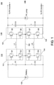
Figure 1 is a schematic diagram of a DC/DC converter according to an embodiment of the present invention. -
Figure 2 is a schematic diagram of a DC/DC converter according to another embodiment of the present invention which is not covered by the subject-matter of the claims. -
Figure 3 is a control structure for a DC/DC converter according to an embodiment of the present invention. -
Figure 4 is a schematic diagram of a DC/DC converter controlled by the control structure shown inFigure 2 according to an embodiment of the present invention. -
Figure 5 is a control structure for a DC/DC converter according to an embodiment of the present invention. -
Figure 6 is an exemplary power system employing a DC/DC converter according to an embodiment of the present invention. -
Figure 7 is a control structure for controlling the voltage difference between the voltage across capacitors of the first and second port according to an embodiment of the present invention. - Embodiments of the present invention include a DC/DC converter in which a voltage magnitude at one port can be controlled to be higher than, the same, and lower than the voltage at the opposing port.
- In one aspect, a DC/DC converter system includes the features of
independent claim 1. - The first conversion stage controller and the second conversion stage controller may include one of a proportional-integral-derivative (PID) controller, proportional-integral (PI) controllers, a proportional (P) controller, and a hysteresis controller.
- The outer control loop may include one of a proportional-integral-derivative (PID) controller, proportional-integral (PI) controllers, a proportional (P) controller, and a hysteresis controller for receiving the comparison of the command for voltage or current and the actual voltage or current to control the interface current.
- The first conversion stage may convert a voltage at the first port to an output voltage that is output at the second port when the voltage at the first port is higher than the voltage at the second port. The second conversion stage may convert a voltage at the second port to an output voltage that is output at the second port when the voltage at the second port is higher than the voltage at the first port. Each of the first conversion stage and the second conversion stage may operate to control the voltages at the first and second ports when the voltages at the first and second port are substantially the same.
- The first conversion stage and the second conversion stage are interfaced through first and second inductors or an isolation transformer.
- When the first conversion stage and the second conversion stage are interfaced through first and second inductors, the first inductor has a first terminal connected to a junction of the pair of first switches and a second terminal connected to the junction of the pair of third switches; and a second inductor having a first terminal connected to a junction of the pair of second switches and a second terminal connected to the pair of fourth switches.
- When the first conversion stage and the second conversion stage are interfaced through an isolation transformer, one side of a first winding of the isolation transformer may be connected to the junction of the pair of switches of the first half bridge, and the other side of the first winding may be connected to the junction of the pair of switches of the second half bridge; and one side of a second winding of the isolation transformer may be connected to the junction of the pair of switches of the third half bridge, and the other side of the second winding may be connected to the junction of the pair of switches of the fourth half bridge.
- The first conversion stage may be connected to an energy storage unit at the first port, and the second conversion stage may be connected to a PV array at the second port.
- The DC/DC converter system may also include: a first capacitor coupled to the first half bridge; a second capacitor coupled to the second half bridge; and the control system may further comprise a capacitance control system for controlling a voltage difference between a voltage across the first capacitor and a voltage across the second capacitor, the capacitance control system being configured to: calculate a difference between the voltage across the first capacitor and the voltage across the second capacitor; calculate a duty ratio offset according to the difference between the voltage across the first capacitor and the voltage across the second capacitor; apply the duty ratio offset to the duty value output by the first conversion stage controller.
- The DC/DC converter system may also include: a third capacitor coupled to the third half bridge; a fourth capacitor coupled to the fourth half bridge; and the control system may further comprise a capacitance control system for controlling a voltage difference between a voltage across the third capacitor and a voltage across the fourth capacitor, the capacitance control system being configured to: calculate a difference between the voltage across the first capacitor and the voltage across the second capacitor; calculate a duty ratio offset according to the difference between the voltage across the first capacitor and the voltage across the second capacitor; apply the duty ratio offset to the duty value output by the first conversion stage controller.
- In another aspect, a method for controlling a bidirectional DC/DC converter with the features of independent claim 9 is disclosed.
- The DC/DC converter may further include: first and second capacitors close coupled to the first and second half bridges; and third and fourth capacitors close coupled to the third and fourth have bridges.
- The first conversion stage and the second conversion stage may be interfaced through an isolation transformer, and one side of a first winding of the isolation transformer is connected to the junction of the pair of switches of the first half bridge, and the other side of the first winding is connected to the junction of the pair of switches of the second half bridge, and one side of a second winding of the isolation transformer is connected to the junction of the pair of switches of the third half bridge, and the other side of the second winding is connected to the junction of the pair of switches of the fourth half bridge.
- The first port may be configured to be coupled to an energy storage unit and the second port may be configured to be coupled to a photovoltaic array.
- Reference will now be made to the accompanying drawings, which form a part hereof, and which show, by way of illustration, specific exemplary embodiments. The principles described herein may, however, be embodied in many different forms. The components in the figures are not necessarily to scale, emphasis instead being placed upon illustrating the principles of the invention. Moreover, in the figures, like referenced numerals may be placed to designate corresponding parts throughout the different views.
- In the following description of the invention, certain terminology is used for the purpose of reference only, and is not intended to be limiting. For example, although the terms first, second, etc. may be used herein to describe various elements, these elements should not be limited by these terms. These terms are only used to distinguish one element from another. As used in the description of the invention and the appended claims, the singular forms "a," "an," and "the" are intended to include the plural forms as well, unless the context clearly indicates otherwise. It will also be understood that the term "and/or" as used herein refers to and encompasses any and all possible combinations of one or more of the associated listed terms. It will be further understood that the terms "comprises" and/or "comprising," when used in this specification, specify the presence of stated features, integers, steps, operations, elements, and/or components, but do not preclude the presence or addition of one or more other features, integers, steps operations, elements, components, and/or groups thereof.
- A typical DC/DC converter may be connected to a source, such as a battery, so that the source voltage can be increased (or decreased) to an intermediate DC bus. For example, if a battery voltage ranges from 300-600V, the DC/DC converter may boost this voltage to an output voltage such as 800V at an intermediate DC bus. Such designs require that the output voltage be always higher than the input voltage, while current control can be in either direction (e.g., to charge or discharge the battery). Such designs are restricted to either increasing or decreasing the source voltage
- Embodiments of the present invention include a DC/DC converter that is not limited to either a boost (i.e., increase) or buck (i.e., decrease) operation. The DC/DC converter includes first and second ports with a topology and control system that allow flexibility, in that a voltage magnitude at one port can be controlled to be higher than, the same, and lower than the voltage at the opposing port.
- Embodiments of the present invention include a DC/DC converter and a control system having a control structure for controlling the DC/DC converter to output a desired current, voltage or power reference. Embodiments of the present invention include a DC/DC converter and control system that enables interfacing of high voltage energy storage (e.g., batteries) and photovoltaic (PV) arrays while utilizing lower voltage rating switches (e.g., semiconductor devices such as insulated-gate bipolar transistors (IGBTs), metal-oxide-semiconductor field-effect transistors (MOSFETs), etc. Embodiments of the present invention also include a DC/DC converter and control system that enables interfacing energy storage (e.g., batteries) with PV arrays, where the output/input voltage of the energy storage and the output voltage of the PV arrays have overlapping voltage magnitudes.
- Referring to
Fig. 1 , a DC/DC converter 100 according to an embodiment of the present invention includes afirst conversion stage 110 and asecond conversion stage 120 connected to each other. The first conversion stage is connected to afirst port 130, which may in turn be connected to a power source such as an energy storage unit (e.g., a battery). The second conversion stage is connected to asecond port 140, which may in turn be connected to a power source such as a photovoltaic (PV) array or another power converter (e.g., a power inverter) or a load. The first and second conversion stages 110, 120 form a bi-directional DC/DC converter (i.e., the power flow is bidirectional). In the embodiment shown inFig. 1 , the magnitude of the voltage on the first convertingstage 110 at thefirst port 130 can be higher or lower than or substantially equal (i.e., close to equal) to the magnitude of the voltage on the second converting stage at thesecond port 140. Thus, either side of the DC/DC converter 100 can be used as a buck or a boost converter. It should be noted that, althoughfigure 1 illustrates a battery and a PV-array connected to the first andsecond ports second ports - In an embodiment, the
first conversion stage 110 is operative to convert the voltage at thefirst port 130 to a desired magnitude (i.e., output voltage) at theport 140 when the magnitude of the voltage of theport 130 is higher than the magnitude of the voltage at theport 140. This conversion may be accomplished using any one of a current command, a voltage command or a power reference that is compared to a feedback signal. Thesecond conversion stage 120 is operative to convert theport 140 voltage to a desired magnitude at theport 130 when the magnitude of the voltage atport 140 is greater than the magnitude of the voltage atport 130. This conversion may be accomplished using any one of a current command, a voltage command or a power reference that is compared to a feedback signal. - Accordingly, the DC to DC converter may be implemented in a design where the voltage magnitude at either port may range up to a predetermined voltage, e.g., 1500V on either side. In this example, the voltages on either
port port 130, the voltage can be 800 V, and onport 140, the voltage can be 1500 V, and the current can be controlled to be in either direction (e.g., to either charge or discharge a power source). Similarly,port 130 can be at 1500 V andport 140 can be at 800 V, and current can be controlled to be in either direction. Finally, the voltage magnitude atport 130 can be the substantially equal to the voltage magnitude atport 140, and the current can be controlled to be in either direction. - In an embodiment, the DC/
DC converter 100 comprises two sets of cascaded half bridges. Thefirst conversion stage 110 comprises afirst half bridge 112 and asecond half bridge 114 connected in series. Each of thefirst half bridge 112 and thesecond half bridge 114 comprises a pair of switches Q1, Q2 and Q3, Q4. The second convertingstage 120 comprises athird half bridge 122 and afourth half bridge 124 that are connected in series. Each of thethird half bridge 122 and thefourth half bridge 124 comprises a pair of switches Q5, Q6 and Q7, Q8. - In the embodiment illustrated in
Fig. 1 , the pair of switches Q1, Q2 of thefirst half bridge 112 are connected in series between a first terminal of thefirst port 130 and a junction of thefirst half bridge 112 and the second half bridge 114 (i.e., node connecting first half bridge to second half bridge). The pair of switches Q3, Q4 of thesecond half bridge 114 are connected in series between the junction of thefirst half bridge 112 and the second half bridge 114 (i.e., node connecting first half bridge to second half bridge) and a second terminal of theport 130. The pair of switches of thethird half bridge 122 are connected in series between a first terminal of thesecond port 140 and a junction of thethird half bridge 122 and thefourth half bridge 124. The pair of switches of thefourth half bridge 124 are connected between the junction of thethird half bridge 122 and thefourth half bridge 124 and a second terminal of thesecond port 140. - In an embodiment, the
first conversion stage 110 and the second conversion stage are interfaced using first and second inductors L1 and L2. One terminal of the first inductor L1 is connected to the junction of the pair of switches Q1, Q2 of the first half bridge 112 (i.e., the node connecting the switches Q1 and Q2). The other terminal of the first inductor L1 is connected to the junction of the pair of switches of thethird half bridge 122. One terminal of the second inductor L2 is connected to the junction of the pair of switches Q3, Q4 of thesecond half bridge 114, and the other terminal of the second inductor is connected to the junction of the pair of switches Q7, Q8 of thefourth half bridge 124. - In another embodiment, which is not covered by the subject-matter of the claims, the first and second inductors L1 and L2 may be replaced by an isolation transformer T1 as shown in
Fig. 2 . As illustrated inFig. 2 , one side of a first winding of the isolation transformer T1 is connected to the junction of the pair of switches Q1, Q2 of the first half bridge, and the other side of the first winding is connected to the junction of the pair of switches Q3, Q4 of the second half bridge. One side of a second winding of transformer T1 is connected to the junction of the pair of switches Q5, Q6 of the third half bridge, and the other side of the second winding is connected to the junction of the pair of switches Q7, Q8 of the fourhalf bridge 124. - In the embodiment in which the first and second conversion stages 110 and 120 are interfaced by the inductors L1 and L2 (
Fig. 1 ), the DC/DC converter 100 may further include an optionalcenter point connection 150. Referring toFig. 1 , thecenter point connection 150 may connect the junction of the first and second half bridges 112, 114 to the junction of the third and fourth half bridges 122, 124. Thecenter point connection 150 may be advantageous, for example, in a scenario in which the input/output 130 is connected to energy storage (e.g., battery/batteries) in that the noise on the battery terminals is reduced by the neutral center-point connection. However, there is a design trade-off to this connection in that the ripple performance (i.e. ripple current and voltage on the battery and PV ports) is compromised to some extent. - In an embodiment, each of the half bridges 112, 114, 122, 124 may be close coupled to a DC bus capacitor C1-C4 for filtering and semiconductor voltage overshoot reduction. For example, capacitor C1 is the filter capacitor for the half-bridge formed by Q1 and Q2. Each of these capacitors C1-C4 may be an individual capacitor or may be a series and parallel combination of several discrete capacitors to reach the appropriate rating.
- In an embodiment, switches Q1-Q8 are semiconductor switches with back-body diodes. Examples of semiconductor switches that may be used for Q1-Q8 include, but are not limited to, IGBT, MOSFETs, etc.
- In an embodiment, an energy storage unit may be provided on input/
output side 130 and a PV array and/or a PV inverter may be connected on the input/output side 140. One such layout is shown in the exemplary system ofFig. 6 . For example, the DC/DC converter 100 can be used between an energy storage unit 510 (such as a battery 610) and aPV array 620, and thePV array 620 may have aninverter 630 connected with autility AC grid 650. In this particular layout, it is preferable that the power flow through the DC/DC converter 100 be bidirectional, so that the system has the capability of charging the batteries with power from the PV array, while also being capable of discharging the batteries to the grid by way of the PV inverter. In this case, the battery voltage can be either higher or lower than or roughly equal to the PV voltage with both directions of power flow. When the battery voltage is higher than the PV voltage, the battery side converter (i.e., the first conversion stage 110) is switching. When the battery voltage is lower than the PV voltage, the PV side converter is switching (i.e., the second conversion stage 120). When the voltages are equal or substantially equal (i.e. close to equal), both sides' converters switch. A determination as to whether the voltages are close to equal may be based on design considerations, and programmed into the converter's 100 control system. For example, the voltages may be determined to be substantially equal when the value obtained from subtracting thefirst port 130 voltage magnitude from thesecond port 140 voltage magnitude is less than or equal to a predetermined value. For example, if the port voltages are within 5% or less than each other, it may be determined that they are substantially the same. Therefore, either side of the DC/DC converter 100 can be used as buck or boost. - In an embodiment,
control system 660 may include one or more controllers for controlling theinverter 630 and the DC/DC converter 100. In one embodiment, thecontrol system 660 may include a single controller for controlling each of the DC/DC converter 100 and theinverter 630. In another embodiment, thecontrol system 660 may include separate controllers for the DC/DC converter 100 and the PV inverter. The controllers of thecontrol system 660 may be housed within the DC/DC converter 100 and/orinverter 630 or may be housed separate from one or both. A separate master controller may also be used to send signals to and/or coordinate between the one or more controllers of the DC/DC converter andinverter 630. -
Fig. 3 shows acontrol structure 300 of a control system for controlling a DC/DC converter according to an embodiment of the present invention.Figure 4 is a schematic diagram of a DC/DC converter controlled by thecontrol structure 300 shown inFigure 3 according to an embodiment of the present invention.Figure 4 is similar toFig. 1 , but also includes symbols for certain measurements and gating/switching signals for sending to the switches of the DC/DC converter. - Referring to
Figs. 3 and4 , thecontrol structure 300 includes anouter control loop 310 and aninner control loop 320. Theouter loop 310 controls the magnitude of the voltage, current or power at thefirst port 130 or the second port 120 (in one example, this could be the magnitude of the battery/PV current or the magnitude of the battery/PV voltage). Theinner loop 320 controls the interface inductor current Im1. In the exemplary embodiment shown inFig. 4 , the battery current or voltage is the current or voltage atport 130, and the PV current or voltage is the voltage or current at theport 140. The interface inductor current Im1 is the current at the interface of the first conversion stage and the second conversion stage. In the embodiment in which first and second inductors L1 and L2 are used as the interface of the first and second conversion stages 110, 120 (Figs. 1 and4 ), one or both of the interface inductor currents (e.g. Im1, Im2 or Im1 and Im2) are controlled. In the embodiment in which the first and second inductors are replaced by an isolation transformer T1 (Fig. 2 ), which is not covered by the subject-matter of the claims, theinner loop 320 controls transformer current Im1. It should be understood that although the exemplary embodiment has battery/PV voltage or current as a source, other sources may be coupled to theports outer loop 310 would control the voltage/current/power of one of the first andsecond ports - In the embodiment shown in
Fig. 3 , the controller parameters (e.g., the two PI parameters) may be tuned to adapt to hardware parameters. The tuning may depend on multiple factors, for example: 1) Speed of response required - the control bandwidth of the system - e.g., whether it is desirable for the converter to reach rated current in 1ms or 100ms; and 2) The hardware parameters of the system: inductance, capacitance and switching frequency values. - The
outer control loop 310 receives as one input a command for a certain level (i.e. magnitude) of voltage, current or power at one of thefirst port 130 and the second port 140 (e.g. battery current or PV voltage), and receives as another input feedback of the actual level of voltage, current or power (e.g., actual magnitude of battery current or PV voltage). In the case of a command for power, power is calculated by using values obtained from voltage and current sensors at theport first port 130 or the second port 140). These commands may be generated internally in the DC/DC converter 100's controller based on the desired mode of operation or sent by a master controller. For example, if batteries are to be discharged, a positive battery current command may be used, and if the batteries are to be charged, a negative battery current command may be used. The feedback of battery current or PV voltage is the actual magnitude of the battery current or actual magnitude of the PV voltage that is measured at thefirst port 130 or thesecond port 140. The desired magnitude is then compared to the actual magnitude by, for example, taking the difference between the desired magnitude and actual magnitude. This difference is inputted into acontroller 312 for controlling one of the interface inductor currents (e.g., Im1) through one of the inductors (e.g., Lm1). Thecontroller 312 then outputs the current command Im_cmd for the interface inductor current to theinner control loop 320. Here, the current command Im_cmd may be viewed as a desired magnitude for the interface inductor current that can be compared to the actual magnitude of the interface inductor current in order to calculate a duty value D1 for one or more of the switching signals that are transmitted to the switches Q1-Q8 of the first and second conversion stages 110, 120. - In an embodiment in which the center-
point connection 150 is installed, in addition to controlling the inductor current Im1, thecontrol structure 300 may include additional outer and inner control loops for controlling Im2 in the same manner in which Im1 is controlled. When the center-point connection 150 is omitted, control of Im2 is not necessary, as the inductor current Im2 will be the same as Im1. - In the embodiment shown in
Fig. 3 , thecontrollers - The
inner control loop 320 receives as inputs the inductor current command Im_cmd and the actual magnitude of the inductor current Im1. The inductor current command Im_cmd is then compared to the interface inductor current Im1 by, for example, taking the difference between the inductor current command Im_cmd and the inductor current Im1. This difference is then inputted into acontroller 322 for calculating a duty value D1, which can be used to generate switching signals Gb1p, Gb1n, Gb2p, Gb2n, Gs1p, Gs1n, Gs2p, Gs2n that are input to switches Q1-Q8 (seeFig. 4 ).Controller 322 outputs the duty value or the switching signals Gb1p, Gb1n, Gb2p, Gb2n, Gs1p, Gs1n, Gs2p, Gs2n to the DC/DC converter. The duty value affects the duty cycle of the signals to the switches, which affects the magnitude of the step up/step down of the DC/DC converter 100, and the duty ratio depends on the ratio of the voltages at thefirst port 130 and thesecond port 140 of the DC/DC converter 100. - When the
control structure 300 calculates a duty value, current flowing from the input/output 130 may be defined as positive current (e.g., in an embodiment in which the battery is at the input/output 130, battery discharge current is defined as positive current), and the control structure may control the current of the upper interface inductor Lm1 (it should be understood that the control structure could similarly control the current of any of the interface inductors). Then the duty value (Db1) calculated from the battery side controller is for the gate of IGBT Tb1p (Gb1p). When, for example, the duty value Db1 is 1, Tb1p is fully on, and 0.5 for half on half off, and 0 for fully off. Gb1n may be the reverse of Gb1p with dead time. Gb2p/Gb2n may be ascertained from Gb1p/Gb1n in multiple ways. In one embodiment Gb2p/Gb2n may be ascertained by reversing Gb1p/Gb1n (i.e. Gb2p=Gb1n, Gb2n=Gb1p). In another embodiment, Gb2p/Gb2n may be ascertained by reversing Gb1p/Gb1n and shifting a half cycle (180 degree). Similar logic is applied for input/output side 140 switch signals. - In some situations, only diodes of some IGBTs are needed i.e. the IGBTs should be fully off. For example, when the PV side voltage is sufficiently higher than the battery side (i.e., they are not substantially equal to each other) and current is flowing from the battery side to the PV side, Ts1p/Ts2n should be off and only Ts1n/Ts2p are switching. In an embodiment, it is preferable to NOT turn off the switches gating (i.e., even though these switches are not needed, the switches still receive gate signals). However, the direction of the current is such that the switches do not conduct. Instead, the back body parallel diode conducts. Even though these switches are switching, there is no current through them, so there is no loss. In converters that use MOSFET's, it is desired that the MOSFET channel conduct current rather than the back body diodes - in this case, it is required that the gating not be turned OFF.
- Although the control structure of
Fig. 3 is able to calculate duty cycles of switching signals Gb1p, Gb1n, Gb2p, Gb2n, Gs1p, Gs1n, Gs2p, Gs2n to get the desired output, this control system has difficulty in avoiding switching of thefirst conversion stage 110 and thesecond conversion stage 120 at the same time. When the voltage magnitudes at the port 130 (e.g., battery) and port 140 (e.g., PV array or PV inverter) are different, the switches of only one of thefirst conversion stage 110 and thesecond conversion stage 120 need to be switching. For example, only the switches of the first orsecond conversion stage 120 at the input/output second conversion stage output 130 and a PV array / PV inverter is on input/output side 140, if PV=1000V and Battery = 500V, the batteryside conversion stage 110 should not switch and the PVside conversion stage 120 will have a duty ratio of close to 0.5. - Although the control structure shown in
Fig. 3 can provide control for switching both of the first and second conversion stages 120 to obtain the desired output, this control results in unnecessary switching loss (in this case, if switching all switches at both sides to make the voltage on the interface of the first and second conversion stages lower than both sides of battery and PV voltage, control can be accomplished, but switching loss occurs). -
Fig. 5 is acontrol structure 500 for a DC/DC converter according to an embodiment of the present invention. Thecontrol structure 500 ofFig. 5 controls the DC/DC converter 100 so that only one of thefirst conversion stage 110 and thesecond conversion stage 120 is switching at a time when the voltages at theseconversions stages first conversion stage 110 and thesecond conversion stage 120 are both switching when the voltage magnitudes at thefirst conversion stage 110 and thesecond conversion stage 120 are sufficient close (i.e., their difference is within the predetermined voltage value). In addition, the control structure ofFig. 5 provides for a smooth transition between switching of one of the conversion stages to the other of the conversion stages. - Referring to
Fig. 5 , thecontrol structure 500 comprises an outercontrol loop unit 510 and an innercontrol loop unit 520. The outercontrol loop unit 510 controls one of the ports' (110 or 120) voltage magnitude, current magnitude or power and produces an interface inductor current command Im_cmd (in an embodiment in which the first and second inductors are replaced by an isolation transformer T1 (seeFig. 5 ), which is not covered by the subject-matter of the claims, theinner loop 320 may control transformer current Im1). Theinner control loop 520 receives the inductor current command Im_cmd and generates two different inductor current commands, i.e., a first inductor current command Ib_cmd and a second inductor current command Is_cmd by comparing the interface current command to an interface current comparison value (or in other words, by adjusting the Im_cmd value for the two ports using an interface current comparison value Idelta). Theinner control loop 520 uses the first and second inductor current commands Ib_cmd and Is_cmd to generate first and second duty values Db1 and Ds1. The first duty value Db1 is for controlling the switching of the switches Q1-Q4 of thefirst conversion stage 110, and the second duty value Ds1 is for controlling the switching of the switches Q5-Q8 of thesecond conversion stage 120. - In an embodiment in which the center-
point connection 150 is installed, in addition to controlling the inductor current Im1, thecontrol structure 500 may include additional outer and inner control loops for controlling Im2 in the same manner in which Im1 is controlled. When the center-point connection 150 is omitted, control of Im2 is not necessary, as the inductor current Im2 will be the same as Im1. - In the embodiment shown in
Fig. 5 , thecontrollers - The outer
control loop unit 510 receives as one input a command for voltage magnitude, current magnitude or power at one of the first andsecond ports 130 and 140 (e.g. battery current or PV voltage). The outercontrol loop unit 510 receives as another input feedback of theport Fig. 3 , it should be understood that the battery/PV voltage or current as a source is exemplary, and other sources may be coupled to theports port 130 or 140 (e.g., battery current or actual magnitude of the PV voltage). The desired magnitude is then compared to the actual magnitude by, for example, taking the difference between the desired magnitude and actual magnitude. This difference is inputted into acontroller 512 for controlling one of the interface inductor currents (e.g., Im1) over one of the inductors (e.g., Lm1). Thecontroller 512 then outputs the current command Im_cmd for the interface inductor current to theinner control loop 520. Here, the current command Im_cmd may be a desired magnitude for the interface inductor current that is compared to the actual magnitude of the interface inductor current. - In the
inner control loop 520, interface inductor (Lm1) current (Im1) is controlled by calculating gate duties Db1, Ds1 for switching signals sent to the switches Q1-Q8 to make the magnitude of the current Im1 equal to the magnitude of the current command Im_cmd received from the outer control loop. In the case in which the first andsecond ports port output 130 and a PV array / PV inverter is on input/output side 140, if PV=1000V and Battery = 500V, the batteryside conversion stage 110 should be a constant 1 or 0 switch and the PVside conversion stage 120 will switch according to the duty value Ds1. - It should be noted that, for the DC/
DC converter 100 topology, if a controller makes mistakes as to which side is a higher voltage (i.e., voltage and thefirst conversion stage 110 or second conversion stage 120), there will be a large current disturbance. Considering the case in which the battery is connected to thefirst port 130 and the PV array is connected to thesecond port 140, it can be appreciated that the battery voltage does not change quickly, and it can be treated as constant within a few seconds. However, the PV voltage can and often does change quickly, because the PV voltage is reliant on the amount of sunlight incident on the PV array. If the voltage feedbacks into the control system have errors, it is possible to mistake which side voltage is higher (i.e., which of the voltage magnitude at thefirst port 130 andsecond port 140 is higher). Thus, a current disturbance can easily happen when the PV voltage is fast crossing the battery voltage. - The control structure of the embodiment shown in
Fig. 5 is able to smoothen the transfer from one conversion stage to the other. - In the embodiment shown in
Fig. 5 , theinner control loop 520 includes two controllers, a firstconversion stage controller 522 and a second conversion stage controller 524 (e.g., two PI controls - as noted above, the controllers are not limited to being a PI controller and can be any closed loop controller). The firstconversion stage controller 522 controls a gate duty Db1 for generating switching signals that are output to switches Q1-Q4 of thefirst conversion stage 110, and the secondconversion stage controller 524 controls a gate duty Ds1 for generating switching signals that are output to switches Q5-Q8 of thesecond conversion stage 120. - When implementing the control structure in the embodiment shown in
Fig. 5 , each of thefirst conversion stage 110 and thesecond conversion stage 120 can be thought of as wanting to control Im1 current. However, in reality, there is only one Im1 current to be controlled. By issuing different current commands for the two PI controls as shown inFig. 5 , the result of the twocontrollers 

- Idelta is referred to as an interface current comparison value. The interface current comparison value Idelta can be set as a constant positive value. However, it is preferable to change its value with Im_cmd as in the below equation.

- In the above equations, the interface current comparison value Idelta should be a positive value. Preferable, a minimum limit Idelta_min is set for the interface current comparison value Idelta, so that if Kdrp * abs( Im_cmd ) < Idelta_min, then Idelta = Idelta_min.
- The droop factor Kdrp is preferably a small ratio (e.g., 5-10%, Kdrp = 0.05-0.1). Idelta_min is preferable set to 5% of rated converter current as initial value for tuning.
- The duty ratios Db1 and Ds1 are normally limited to a maximum value of 1. When the voltages and the first and
second port second port second port 

- In accordance with the above equations, in the
inner control loop 520, the interface current command Im_cmd controlled by the outer control loop is compared to/adjusted by the interface current comparison value Idelta in order to output the first and second interface current commands Ib_cmd and Is_cmd. In the embodiment ofFig. 5 , the comparison to the interface current comparison value Idelta involves subtracting the interface current comparison value Idelta from the interface current command Im_cmd to generate the first interface current command Ib_cmd and adding the interface current comparison value Idelta to the interface current command Im_cmd to generate the second interface current command. The first and second interface current commands are then compared to the actual value of the interface current Im1 (e.g., the interface current over inductor L1 (Fig. 1 ) or the transformer current (Fig. 2 ) by, for example, subtracting the actual value of the interface current Im1 from these values, and the result of the comparison is output to the first and secondconversion stage controllers conversion stage controllers 522 then generate gate duty values Db1 and Ds1 for generating switching signals for the first and second conversion stages 110 and 120, respectively. - When controlling as above, it should be noted that the real Lm1 current Im1 can be different from the command Im_cmd. However, this is not problematic, because the final target is battery current or PV voltage, which is controlled by the
outer control loop 510. The current command Im_cmd will be auto adjusted by theouter control loop 510. - For the feedback to the inner control unit, the interface current Im1 is sampled. It should be noted that the interface inductor current Im1 can include high frequency ripple. The ripple is roughly linear up/down. The ripple frequency is equal to or double of the switching frequency of the switches of the first and second conversion stages 110 and 120. The ripple amplitude depends on the ripple frequency, the magnitude of the inductances Lm1 & Lm2 and the difference between first port 130 (e.g. battery) and second port 140 (e.g. PV) voltages. If the sample frequency for Lm1 current feedback is the same as the switching frequency, the sampled value for Lm1 current can have error. Therefore, it is preferable to sample at the middle point of the ripple, as otherwise, the sampled value is different from real average current. However, in any event, since Lm1 is not the final target, the outer control loop - which receives as inputs both the final target value (e.g., battery current or PV voltage) and its actual value - will auto adjust for errors in the Lm1 current.
- When the DC/
DC converter 100 is coupled to an energy storage (e.g., battery) and a PV array / inverter, for theouter control loop 310, the control target can be battery current or PV voltage, and thecontrol structure 500 can transfer between these two targets depending on which one the user wants to control. When the target is battery current, the actual battery current is sampled for the feedback in theouter loop 310; and when the target is PV voltage, actual PV voltage is sampled for the feedback in theouter loop 310. It should be noted that when battery current is sampled, this sampling is more critical than when sampling the interface inductor L1 current for the inner loop. Because interface inductor current Im1 is not the final target, the accuracy of Im1 current sampling is not as significant, because, as mentioned above, theouter control loop 510 will auto adjust for theinner control loop 520. Because battery current is the final target, its' accuracy when sampling is more significant. - As discussed above, on the terminals of the first conversion stage 110 (e.g., the battery side of the converter), there are capacitors C1 and C2. When there is current between the battery and the DC/DC converter, the (battery) current will include some ripples or oscillations. The ripple frequency is the switching frequency (or double). Assuming the switching frequency is fixed, the battery current ripple amplitude mainly depends on the impedance between the battery and the capacitors of the converter. If the capacitors on the battery side of the converter are not large enough or/and the switching frequency is not high enough, the battery current ripple may be over the specification. An additional inductor may be provided between the battery and the converter.
- Besides the fact that the battery current feedback needs more accuracy than Lm1 current, the middle point of the battery current moves when the impedance between the battery and the converter changes. Thus, it is difficult to sample the middle point of the battery current or to correct the error caused by sampling at the wrong point of the battery current. Therefore, in an embodiment, the battery current for the feedback is sampled at a higher frequency than the switching frequency of the switches of the first and second conversion stages 110 and 120. For example, in an embodiment, 16 points of the battery current are sampled during one switching cycle, and then the average of these 16 points is calculated and provided as the feedback for the battery current control. An increase in the number of sampling points can increase the delay and slow down the battery current control. Therefore, the number of sampling points may be determined based on the response time that is desired. Furthermore, if the battery current ripple is high, the number of sampling points may be increased..
-
Fig. 7 is a control structure/system for controlling the voltage difference between the voltage across capacitors of the first and second port according to an embodiment of the present invention. It is desirable to maintain the difference between the voltage over capacitor C1 and the voltage over capacitor C2 on the first port 130 (and similarly the voltage over capacitor C3 and the voltage over capacitor C4 on the second port 140) close to zero.Fig 7 shows a control structure/system that can be provided along with the control structure ofFig. 3 orFig. 5 to achieve this. This control structure 700 can be provided in on the same or separate physical controller as the control structure ofFig. 5 . - Referring to
Fig. 7 , the voltages across capacitors C1 and C2 (Figs 1 and2 ) are measured and their difference is calculated (Vc1 - Vc2). This value is then multiplied by 1 if the direction of the current flow in inductor L1 is fromport 130 toport 140. Current in L2 or current in transformer T1 may also be used for this purpose. If the current flow is in the reverse direction, then the voltage difference is multiplied by a -1 instead. A low-pass filter 710 may be used to filter the measured current and the direction of the filtered current may also be used. - The value thus obtained is then inputted into a
controller 702 for calculating the duty ratio offset that must be applied to the duty ratio obtained from controller 522 (infigure 5 ). The output of this controller is added to the output ofcontroller 522 for generating the switching signals for the switches Q1 and Q2 of thefirst half bridge 112 and subtracted from the output of thecontroller 522 for generating the switching signals for the switches Q3 and Q4 of thesecond half bridge 114. - The
controller 702 may be a closed loop controller such as a PI controller, a proportional-integral-derivative (PID) controller, a proportional (P) controller, a hysteresis controller, etc. - A similar approach is taken to maintain a close to zero voltage difference between capacitors C3 and C4 of
port 140. The voltages across capacitors C3 and C4 are measured and their difference is calculated (Vc3 - Vc4). This value is then multiplied by 1 if the direction of the current flow in inductor L1 is fromport 130 toport 140. Current in L2 or current in transformer T1 may also be used for this purpose. If the current flow is in the reverse direction, then the voltage difference is multiplied by -1 instead. A low pass filter may be used to filter the measured current and the direction of the filtered current (sign) may also be used. - The value thus obtained is then inputted into a controller for calculating the duty ratio offset that should be applied to the duty ratio obtained from controller 524 (in
fig 5 ). The output of this controller is subtracted from the output ofcontroller 524 for generating the switching signals for thethird half bridge 122 and added to the output of 524 for generating the switching signals for thefourth half bridge 124. - Although in certain exemplary embodiments discussed above, the DC/
DC converter 100 is described as being coupled between energy storage and a PV array / inverter, it should be understood the present invention is not limited to this application. It will be readily understood to a person of ordinary skill in the art that embodiments of the present invention are suitable for additional applications, such as applications where DC/DC conversion is required with overlapping voltages on the first and second 130 and 140 input/output sides. Additional examples include back up power in variable frequency drives (VFD) applications. The DC/DC converter may be interfaced with a VFD's DC bus. When the grid voltage is present, the DC bus voltage is established by the grid and the VFD is feeding the motor. When the grid goes away (e.g., a power outage), the DC/DC converter can hold up the DC bus by discharging the batteries into the VFD, allowing the VFD to run without interruption. - The
control structure control structure - It will be apparent to those skilled in the art that various modifications and variations can be made to the disclosed power system without departing from the scope of the claims. Other embodiments of the present disclosure will be apparent to those skilled in the art from consideration of the specification and practice of the present disclosure. It is intended that the specification and examples be considered as exemplary only, with a true scope of the present disclosure being indicated by the following claims.
Claims (9)
- A DC/DC converter system comprising:
a bidirectional DC/DC converter (100) for converting between voltage levels at first and second ports (130,140), the bidirectional DC/DC converter (100) comprising:a first conversion stage (110) connected to the first port (130) and comprising a plurality of switches (Q1,Q2,Q3,Q4); anda second conversion stage interfaced with the first conversion stage (110), the second conversion stage being connected to the second port (140) and comprising a plurality of switches (Q5,Q6,Q7,Q8);a control system (660) for controlling the DC/DC converter (100), the control system (660) comprising:an outer control loop unit (510) configured to compare a command for any one of a voltage level, a current level or power at one of the first port (130) and the second port (140) to an actual value of voltage level, current level or power level at the one of the first port (130) and the second port (140) and to output an interface current command based on the comparison;an inner control loop unit (520) configured to compare the interface current command (Im_cmd) to an actual value of interface current (Im1) at the interface of the first and second conversion stages (110,120), and to control a switching signal duty value based on the comparison; andwherein the first conversion stage (110) comprises a first half bridge (112) and a second half bridge (114) connected in series between a first terminal and a second terminal of a first port (130);the second conversion stage (120) comprises a third half bridge (122) and a fourth half bridge (124) connected in series between a third terminal and a fourth terminal of a second port (140);the first half bridge (112) comprises a pair of first switches (Q1,Q2) connected in series between the first terminal of the first port (130) and a junction of the first half bridge (112) and the second half bridge (112), and the second half bridge (114) comprises a pair of second switches (Q3,Q4) connected in series between the junction of the first half bridge (112) and the second half bridge (114) and the second terminal of the first port; andthe third half bridge (122) comprises a pair of third switches (Q5,Q6) connected in series between the third terminal of the second port (14) and a junction of the third half bridge (122) and the fourth half bridge (124), and the fourth half bridge (124) comprises a pair of fourth switches (Q7,Q8) connected in series between a junction of the third half bridge (122) and the fourth half bridge (124) and the fourth terminal of the second port (140),wherein the first conversion stage and the second conversion stage are interfaced through first and second inductors (L1, L2), wherein the first inductor (L1) has a first terminal connected to a junction between the pair of first switches (Q1, Q2) and a second terminal connected to a junction between the pair of third switches (Q5, Q6) and wherein the second inductor (L2) has a first terminal connected to a junction between the pair of second switches (Q3, Q4) and a second terminal connected to a junction between the pair of fourth switches (Q7, Q8),wherein the inner control loop unit (520) comprises a first conversion stage controller (522) and a second conversion stage controller (524), and the inner control loop unit (520) is further configured to:compare the interface current command (Im_cmd) to an interface current comparison value (Idelta) to generate first and second interface current commands (Ib_cmd, Is_cmd); wherein the interface current comparison value (Idelta) is defined by: wherein Kdrp is a positive droop factor, wherein the inner control loop unit is further configured to compare the first and second interface current commands to the actual value of interface current, wherein:the first conversion stage controller (522) is configured to control a duty value of a switching signal for the first conversion stage (110) according to the comparison of the first interface current command and the actual value of interface current; and the second conversion stage controller (524) is configured to control a duty value of a switching signal for the second conversion stage (120) according to a comparison of the second interface current command and the actual value of interface current,wherein in comparing the interface current command (Im_cmd) to an interface current comparison value (Idelta), the inner control loop unit (520) is configured to:subtract the interface current comparison value (Idelta) from the interface current command (Im_cmd) to generate the first interface current command (Ib_cmd);add the interface current comparison value (Idelta) to the interface current command to generate the second interface current command (Is_cmd);compare the first interface current command (Ib_cmd) to the actual value of interface current (Im1);and control, by the first conversion stage controller (522), the duty value of the switching signal for the first conversion stage (110) based on the comparison; andcompare the second interface current command (Ib_cmd) to the actual value of the interface current (Im1), and control, by the second conversion stage controller (524), the duty value of the switching signal for the second conversion stage (120) based on the comparison.
 - The DC/DC converter system of claim 1, wherein the first conversion stage controller (522) and the second conversion stage controller (524) comprise one of a proportional-integral-derivative (PID) controller, proportional-integral (PI) controllers, a proportional (P) controller, and a hysteresis controller.
- The DC/DC converter system of any one of claims 1-2, wherein the outer control loop (310) comprises one of a proportional-integral-derivative (PID) controller, proportional-integral (PD) controllers, a proportional (P) controller, and a hysteresis controller for receiving the comparison of the command for voltage or current and the actual voltage or current to control the interface current.
- The DC/DC converter system of any one of claims 1-3, wherein the first conversion stage (110) converts a voltage at the first port (130) to an output voltage that is output at the second port (140) when the voltage at the first port (130) is higher than the voltage at the second port (140), the second conversion stage (120) converts a voltage at the second port (140) to an output voltage that is output at the second port (140) when the voltage at the second port (140) is higher than the voltage at the first port (130), and each of the first conversion stage (110) and the second conversion stage (120) operate to control the voltages at the first and second ports (130,140) when the voltages at the first and second port (140) are the same.
- The DC/DC converter system of any one of claims 1-4, wherein the first conversion stage (110) is connected to an energy storage unit (510) at the first port (130), and the second conversion stage (120) is connected to a PV array (620) at the second port (140).
- The DC/DC converter system of claim 5, further comprising: a first capacitor (C1) coupled to the first half bridge (112);a second capacitor (C2) coupled to the second half bridge (114); andthe control system (660) further comprises a capacitance control system (660) for controllinga voltage difference between a voltage across the first capacitor (C1) and a voltage across thesecond capacitor (C2), the capacitance control system (660) being configured to:calculate a difference between the voltage across the first capacitor (C1) and the voltage across the second capacitor (C2);calculate a duty ratio offset according to the difference between the voltage across the first capacitor (C1) and the voltage across the second capacitor (C2);apply the duty ratio offset to the duty value output by the first conversion stage controller (522).
- The DC/DC converter system of any one of claims 5-6, further comprising: a third capacitor (C3) coupled to the third half bridge (122);a fourth capacitor (C4) coupled to the fourth half bridge (124); andthe control system (660) further comprises a capacitance control system (660) for controllinga voltage difference between a voltage across the third capacitor (C3) and a voltage across the fourth capacitor (C4), the capacitance control system (660) being configured to:calculate a difference between the voltage across the third capacitor (C3) and the voltage across the fourth capacitor (C4);calculate a duty ratio offset according to the difference between the voltage across the thirdcapacitor (C3) and the voltage across the fourth capacitor (C4);apply the duty ratio offset to the duty value output by the second conversion stage (120) controller (524).
- A method for controlling a bidirectional DC/DC converter (100) comprising a first conversion stage (110) including a first half bridge (112) and a second half bridge (114) connected in series between a first terminal and a second terminal of a first port (130) and interfaced with a second conversion stage (120) including a third half bridge (122) and a fourth half bridge (124) connected in series between a third terminal and a fourth terminal of a second port (140),the first half bridge (112) including a pair of first switches (Q1, Q2) connected in series between the first terminal of the first port (130) and a junction of the first half bridge (112) and the second half bridge (114), and the second half bridge (114) including a pair of second switches (Q3, Q4) connected in series between the junction of the first half bridge (112) and the second half bridge (114) and the second terminal of the first port (130); andthe third half bridge (122) including a pair of third switches (Q5, Q6) connected in series between a junction of the third half bridge (122) and the fourth half bridge (124), and the fourth half bridge (124) including a pair of fourth switches (Q7, Q8) connected in series between the junction of the third half bridge (122) and the fourth half bridge (124) and the fourth terminal of the second port (140),wherein the first conversion stage and the second conversion stage are interfaced through first and second inductors (L1, L2), wherein the first inductor (L1) has a first terminal connected to a junction between the pair of first switches (Q1, Q2) and a second terminal connected to a junction between the pair of third switches (Q5, Q6) and wherein the second inductor (L2) has a first terminal connected between a junction of the pair of second switches (Q3, Q4) and a second terminal connected between a junction of the pair of fourth switches (Q7, Q8),the method comprising:comparing a command for one of a current level, a voltage level or power at one of the first and second ports (130,140) to an actual value of current level, voltage level or power at the one of the first and second ports (130,140), and outputting an interface current command based on the comparison; andcomparing the interface current command to an actual value of an interface current at the interface of the first and second conversion stages (110,120), and controlling a switching signal based on the comparison,_ the step of comparing the interface current command to an actual value of an interface current at an interface of the first and second conversion stages (110,120), and controlling a switching signal based on the comparison comprising:comparing the interface current command (Im_cmd) to an interface current comparison value (Idelta) to generate first and second interface current commands (Ib_cmd, Is_cmd); wherein the interface current comparison value (Idelta) is defined by:
 wherein Kdrp is a positive droop factor, and comprising further the steps of comparing the first and second interface current commands (Ib_cmd, Is_cmd) to the actual value of interface current (Im1);controlling a duty value of a switching signal for the first conversion stage (110) according to the comparison of the first interface current command (Is_cmd) and the actual value of interface current (Im1); andcontrolling a duty value of a switching signal for the second conversion stage (120) according to a comparison of the second interface current command (Ib_cmd) and the actual value of interface current (Im1),wherein the step of comparing the interface current command to an interface current comparison value to generate first and second interface current commands and controlling the duty values of switching signals for the first and second conversion stages (110,120) comprises:subtracting the interface current comparison value (Idelta) from the interface current command (Im_cmd) to generate the first interface current command (Ib_cmd); adding the interface current comparison value (Idelta) to the interface current command (Im_cmd) to generate the second interface current command (Is_cmd);comparing the first interface current command (Im_cmd) to the actual value of interface current (Im1), and controlling the duty value of the switching signal for the first conversion stage (110) based on the comparison; andcomparing the second interface current command (Is_cmd) to the actual value of the interface current (Im1), andcontrolling the duty value of the switching signal for the second conversion stage (120) based on the comparison.
 - The method for controlling a bidirectional DC/DC converter (100) of claim 8,
wherein the first conversion stage (110) is connected to an energy storage unit (510) at the first port (130), and the second conversion stage (120) is connected to a PV array (620) at the second port (140).
Applications Claiming Priority (2)
| Application Number | Priority Date | Filing Date | Title |
|---|---|---|---|
| US201762506315P | 2017-05-15 | 2017-05-15 | |
| PCT/US2018/017964 WO2018212813A1 (en) | 2017-05-15 | 2018-02-13 | Dc/dc converter and control thereof |
Publications (2)
| Publication Number | Publication Date |
|---|---|
| EP3625883A1 EP3625883A1 (en) | 2020-03-25 |
| EP3625883B1 true EP3625883B1 (en) | 2025-04-30 |
Family
ID=61283369
Family Applications (1)
| Application Number | Title | Priority Date | Filing Date |
|---|---|---|---|
| EP18707538.7A Active EP3625883B1 (en) | 2017-05-15 | 2018-02-13 | Dc/dc converter and control thereof |
Country Status (9)
| Country | Link |
|---|---|
| US (2) | US10749435B2 (en) |
| EP (1) | EP3625883B1 (en) |
| JP (2) | JP7166293B2 (en) |
| KR (1) | KR102653533B1 (en) |
| CN (1) | CN110892628B (en) |
| AU (2) | AU2018268716A1 (en) |
| NZ (1) | NZ760094A (en) |
| WO (1) | WO2018212813A1 (en) |
| ZA (1) | ZA201908321B (en) |
Families Citing this family (21)
| Publication number | Priority date | Publication date | Assignee | Title |
|---|---|---|---|---|
| JP6883489B2 (en) * | 2017-08-22 | 2021-06-09 | ダイヤモンド電機株式会社 | converter |
| US10998820B2 (en) | 2018-08-23 | 2021-05-04 | Epc Power Corporation | Stacked DC-DC converter |
| CN111446860B (en) | 2019-01-16 | 2021-09-21 | 台达电子企业管理(上海)有限公司 | DC/DC converter and control method thereof |
| CN111446861B (en) * | 2019-01-16 | 2021-02-26 | 台达电子企业管理(上海)有限公司 | DC/DC converter and control method thereof |
| US12341418B2 (en) | 2019-06-24 | 2025-06-24 | Ge Grid Solutions Llc | Control circuit and method for bus voltage variation in power converters |
| KR102585282B1 (en) * | 2019-07-18 | 2023-10-04 | 엘에스일렉트릭(주) | Dc-dc converter in power transform system |
| US11101742B2 (en) * | 2020-01-03 | 2021-08-24 | Prince Sultan University | Buck-chopper and bi-directional chopper for multilevel cascaded H-bridge inverters |
| TWI743652B (en) * | 2020-01-09 | 2021-10-21 | 呂錦山 | Novel tt control zvs power inversion circuits |
| CN111664287B (en) * | 2020-05-21 | 2022-04-19 | 四川虹美智能科技有限公司 | Constant-current control device, method and system for electromagnetic valve |
| CN112600422A (en) * | 2020-12-11 | 2021-04-02 | 浙江师范大学 | Leading adjustable boost circuit of pulse power supply for electrostatic precipitator |
| KR20220096817A (en) * | 2020-12-31 | 2022-07-07 | 영화테크(주) | Power converter for electric vehicles |
| US11916424B2 (en) * | 2021-05-26 | 2024-02-27 | Rivian Ip Holdings, Llc | Controllers, devices, and methods for controlling direct current fast charging devices |
| CN113489325B (en) * | 2021-07-27 | 2025-05-09 | 上海正泰电源系统有限公司 | DC-DC bidirectional converter and control method thereof |
| CN113890343A (en) * | 2021-09-14 | 2022-01-04 | 宁波吉利罗佑发动机零部件有限公司 | Control method, device and system of boost converter and readable storage medium |
| CN118216054A (en) * | 2021-09-17 | 2024-06-18 | 杰耐瑞克动力系统公司 | Generator system with automatic power control |
| US11645222B1 (en) * | 2022-01-11 | 2023-05-09 | United States Of America As Represented By The Secretary Of The Air Force | Real time generation of differential serial bus traffic |
| CN114567176B (en) * | 2022-02-15 | 2024-08-23 | 中国科学院电工研究所 | Bidirectional direct current converter and wide-range operation modulation method thereof |
| KR102591100B1 (en) * | 2022-03-11 | 2023-10-19 | 가천대학교 산학협력단 | A energy flow and voltage control method for the distributed DC nanogrid system |
| US20240097572A1 (en) * | 2022-09-15 | 2024-03-21 | Virginia Tech Intellectual Properties, Inc. | Reduced common mode voltage emission converter |
| CN119727382A (en) * | 2023-09-28 | 2025-03-28 | 台达电子工业股份有限公司 | Power converter and power conversion method |
| US20250183807A1 (en) * | 2023-11-30 | 2025-06-05 | Rivian Ip Holdings, Llc | Dual active bridge control to minimize dc link resonance |
Citations (6)
| Publication number | Priority date | Publication date | Assignee | Title |
|---|---|---|---|---|
| US20110101944A1 (en) * | 2009-10-29 | 2011-05-05 | Renesas Electronics Corporation | Voltage boosting/lowering circuit |
| US20110187336A1 (en) * | 2010-01-29 | 2011-08-04 | Intersil Americas Inc. | Non-inverting buck boost voltage converter |
| EP2768130A1 (en) * | 2013-02-19 | 2014-08-20 | Siemens Aktiengesellschaft | Direct current converter |
| US20150244259A1 (en) * | 2014-02-21 | 2015-08-27 | Airbus Operations Gmbh | Bipolar high-voltage network and method for operating a bipolar high-voltage network |
| US20160072312A1 (en) * | 2013-07-08 | 2016-03-10 | Murata Manufacturing Co., Ltd. | Power conversion circuit, power transmission system, and power conversion system |
| EP1689070B1 (en) * | 2005-02-08 | 2016-04-13 | Linear Technology Corporation | Current-mode control for switched step up-step down regulators |
Family Cites Families (35)
| Publication number | Priority date | Publication date | Assignee | Title |
|---|---|---|---|---|
| AUPQ775100A0 (en) * | 2000-05-26 | 2000-06-15 | Cleansun Pty Ltd | Power conversion system |
| DE10038814A1 (en) * | 2000-08-09 | 2002-02-21 | Abb Research Ltd | High voltage direct current transformer |
| US6636431B2 (en) * | 2000-12-04 | 2003-10-21 | Nec Tokin Corporation | Symmetrical DC/DC converter |
| GB2376357B (en) * | 2001-06-09 | 2005-05-04 | 3D Instr Ltd | Power converter and method for power conversion |
| US6437462B1 (en) * | 2001-12-10 | 2002-08-20 | Delphi Technologies, Inc. | Bi-directional DC/DC converter and control method therefor |
| JP2006254518A (en) | 2005-03-08 | 2006-09-21 | Yaskawa Electric Corp | Chopper device and control method thereof |
| CN100583615C (en) * | 2005-04-01 | 2010-01-20 | Nxp股份有限公司 | Resonant converter and its control device and control method |
| US7157888B2 (en) * | 2005-06-06 | 2007-01-02 | Aimtron Technology Corp. | Light loading control circuit for a buck-boost voltage converter |
| US7944191B2 (en) * | 2005-10-14 | 2011-05-17 | Monolithic Power Systems, Inc. | Switching regulator with automatic multi mode conversion |
| RU2393618C1 (en) * | 2006-03-22 | 2010-06-27 | Мицубиси Денки Кабусики Кайся | Bidirectional intermediate booster transformer of direct current, control system of railway carriage drive, and feeder system of contact network power supply |
| KR100975485B1 (en) * | 2006-03-22 | 2010-08-11 | 미쓰비시덴키 가부시키가이샤 | Two-way step-down DCC converter device, railway vehicle drive control system, electric railway feeding system |
| CN101647182B (en) * | 2006-12-30 | 2013-01-30 | 先进模拟科技公司 | High Efficiency DC/DC Voltage Converter Including Boost Inductive Switching Pre-Regulator and Capacitive Switching Post-Converter |
| CN100461601C (en) * | 2007-03-16 | 2009-02-11 | 华为技术有限公司 | A system and method for realizing isolated high-frequency switch DC-DC conversion |
| WO2009030275A1 (en) * | 2007-09-05 | 2009-03-12 | Abb Technology Ag | Voltage source converter for high voltage direct current power transmission |
| US7808217B2 (en) * | 2007-10-18 | 2010-10-05 | Analog Devices, Inc. | DC to DC converter |
| WO2010086071A1 (en) * | 2009-01-27 | 2010-08-05 | Abb Research Ltd | Controlling a high-voltage direct-current (hvdc) link |
| US7768245B1 (en) * | 2009-04-28 | 2010-08-03 | Analog Devices, Inc. | Emulator circuit, a controller for a switched mode power supply, and a switched mode power supply |
| TWI389438B (en) * | 2009-11-02 | 2013-03-11 | Analog Integrations Corp | Voltage converter with high efficiency |
| CN102906983B (en) | 2010-07-15 | 2015-06-03 | Abb技术有限公司 | Cell based DC/DC converter |
| JP6038042B2 (en) * | 2010-12-22 | 2016-12-07 | フィリップス ライティング ホールディング ビー ヴィ | Power converter device for driving a solid state lighting load |
| EP2495858A1 (en) | 2011-03-01 | 2012-09-05 | Rheinisch-Westfälisch-Technische Hochschule Aachen | Bidirectional direct current converter |
| CN102222958B (en) * | 2011-06-21 | 2013-10-16 | 清华大学深圳研究生院 | Vehicle-mounted bidirectional charger for electric automobile |
| US9019732B2 (en) * | 2011-07-04 | 2015-04-28 | Abb Technology Ag | High voltage DC/DC converter |
| JP5762617B2 (en) | 2012-02-14 | 2015-08-12 | 三菱電機株式会社 | DC / DC converter |
| US9389617B2 (en) * | 2013-02-19 | 2016-07-12 | Nvidia Corporation | Pulsed current sensing |
| WO2015108613A1 (en) | 2014-01-15 | 2015-07-23 | Abb Technology Ag | Interleaved multi-channel, multi-level, multi-quadrant dc-dc converters |
| JP6185860B2 (en) | 2014-02-27 | 2017-08-23 | 株式会社 日立産業制御ソリューションズ | Bidirectional converter |
| US9602021B2 (en) * | 2014-03-07 | 2017-03-21 | General Electric Company | Hybrid high voltage direct current converter system and method of operating the same |
| US10020747B2 (en) | 2014-04-15 | 2018-07-10 | Danmarks Tekniske Universitet | Resonant DC-DC power converter assembly |
| US9882472B2 (en) * | 2014-09-25 | 2018-01-30 | Intel Corporation | Techniques for power supply topologies with capacitance management to reduce power loss associated with charging and discharging when cycling between power states |
| US9809119B2 (en) * | 2015-01-13 | 2017-11-07 | General Electric Company | Bi-directional DC-DC power converter for a vehicle system |
| TWI555319B (en) * | 2015-01-22 | 2016-10-21 | 通嘉科技股份有限公司 | Single-inductor multiple-output power converter employing adaptive gate biasing technology |
| US9973099B2 (en) | 2015-08-26 | 2018-05-15 | Futurewei Technologies, Inc. | AC/DC converters with wider voltage regulation range |
| US9893633B1 (en) * | 2016-03-23 | 2018-02-13 | The Florida State University Research Foundation, Inc. | Modular multilevel DC-DC converter and associated method of use |
| CN105932867B (en) | 2016-06-30 | 2018-11-06 | 阳光电源股份有限公司 | Bus capacitor charging method, controller and dcdc converter |
-
2018
- 2018-02-13 KR KR1020197037050A patent/KR102653533B1/en active Active
- 2018-02-13 WO PCT/US2018/017964 patent/WO2018212813A1/en not_active Ceased
- 2018-02-13 AU AU2018268716A patent/AU2018268716A1/en not_active Abandoned
- 2018-02-13 NZ NZ760094A patent/NZ760094A/en unknown
- 2018-02-13 JP JP2019563624A patent/JP7166293B2/en active Active
- 2018-02-13 CN CN201880046888.9A patent/CN110892628B/en active Active
- 2018-02-13 EP EP18707538.7A patent/EP3625883B1/en active Active
- 2018-02-13 US US15/895,565 patent/US10749435B2/en active Active
-
2019
- 2019-12-12 ZA ZA2019/08321A patent/ZA201908321B/en unknown
-
2020
- 2020-07-21 US US16/934,839 patent/US11757361B2/en active Active
-
2022
- 2022-10-25 JP JP2022170702A patent/JP7425155B2/en active Active
-
2023
- 2023-05-13 AU AU2023202994A patent/AU2023202994B2/en active Active
Patent Citations (6)
| Publication number | Priority date | Publication date | Assignee | Title |
|---|---|---|---|---|
| EP1689070B1 (en) * | 2005-02-08 | 2016-04-13 | Linear Technology Corporation | Current-mode control for switched step up-step down regulators |
| US20110101944A1 (en) * | 2009-10-29 | 2011-05-05 | Renesas Electronics Corporation | Voltage boosting/lowering circuit |
| US20110187336A1 (en) * | 2010-01-29 | 2011-08-04 | Intersil Americas Inc. | Non-inverting buck boost voltage converter |
| EP2768130A1 (en) * | 2013-02-19 | 2014-08-20 | Siemens Aktiengesellschaft | Direct current converter |
| US20160072312A1 (en) * | 2013-07-08 | 2016-03-10 | Murata Manufacturing Co., Ltd. | Power conversion circuit, power transmission system, and power conversion system |
| US20150244259A1 (en) * | 2014-02-21 | 2015-08-27 | Airbus Operations Gmbh | Bipolar high-voltage network and method for operating a bipolar high-voltage network |
Non-Patent Citations (1)
| Title |
|---|
| ZHOU JIANAN ET AL: "Control strategy of Li-Ion Battery module in Super UPS", 2014 INTERNATIONAL POWER ELECTRONICS AND APPLICATION CONFERENCE AND EXPOSITION, IEEE, 5 November 2014 (2014-11-05), pages 1236 - 1241, XP032734773, DOI: 10.1109/PEAC.2014.7038039 * |
Also Published As
| Publication number | Publication date |
|---|---|
| EP3625883A1 (en) | 2020-03-25 |
| CA3067365A1 (en) | 2018-11-22 |
| AU2023202994A1 (en) | 2023-06-01 |
| JP7425155B2 (en) | 2024-01-30 |
| CN110892628A (en) | 2020-03-17 |
| US20180331625A1 (en) | 2018-11-15 |
| JP7166293B2 (en) | 2022-11-07 |
| AU2018268716A1 (en) | 2020-01-16 |
| JP2023002744A (en) | 2023-01-10 |
| US20210006164A1 (en) | 2021-01-07 |
| KR102653533B1 (en) | 2024-04-02 |
| KR20200056957A (en) | 2020-05-25 |
| AU2023202994B2 (en) | 2024-02-15 |
| US10749435B2 (en) | 2020-08-18 |
| CN110892628B (en) | 2024-07-26 |
| ZA201908321B (en) | 2021-04-28 |
| WO2018212813A1 (en) | 2018-11-22 |
| JP2020520227A (en) | 2020-07-02 |
| NZ760094A (en) | 2021-07-30 |
| US11757361B2 (en) | 2023-09-12 |
Similar Documents
| Publication | Publication Date | Title |
|---|---|---|
| AU2023202994B2 (en) | DC/DC Converter and Control Thereof | |
| Khan et al. | A highly reliable and high-efficiency quasi single-stage buck–boost inverter | |
| EP2949035B1 (en) | Ac-ac converter device | |
| EP2523330A2 (en) | Matrix converter | |
| WO2006090675A1 (en) | Power converter | |
| US20180019688A1 (en) | Half Bridge Inverter Units and Inverter Thereof | |
| WO2016125682A1 (en) | Dc/dc converter | |
| JP5362657B2 (en) | Power converter | |
| Yadeo et al. | A new five level dual active bridge DC-DC converter for solid state transformer | |
| Hassan et al. | Double modulation control (DMC) for dual full bridge current flow controller (2FB-CFC) | |
| US12034301B2 (en) | Multi-way power controller and related methods | |
| CN117318504A (en) | Single-stage multi-channel AC-DC conversion circuit | |
| US12301121B2 (en) | System and method for a partial power transfer between two DC sources | |
| CA3067365C (en) | Dc/dc converter and control thereof | |
| CA2694507C (en) | Method for operation of a converter circuit, and apparatus for carrying out the method | |
| Haryani et al. | Design and Control of GaN based Three-Phase/Single-Phase Combo Three-Level Flying Capacitor PFC for OBC Applications | |
| Akar | A bidirectional multi-phase multi-input DC-DC converter |
Legal Events
| Date | Code | Title | Description |
|---|---|---|---|
| STAA | Information on the status of an ep patent application or granted ep patent |
Free format text: STATUS: UNKNOWN |
|
| STAA | Information on the status of an ep patent application or granted ep patent |
Free format text: STATUS: THE INTERNATIONAL PUBLICATION HAS BEEN MADE |
|
| PUAI | Public reference made under article 153(3) epc to a published international application that has entered the european phase |
Free format text: ORIGINAL CODE: 0009012 |
|
| STAA | Information on the status of an ep patent application or granted ep patent |
Free format text: STATUS: REQUEST FOR EXAMINATION WAS MADE |
|
| 17P | Request for examination filed |
Effective date: 20191212 |
|
| AK | Designated contracting states |
Kind code of ref document: A1 Designated state(s): AL AT BE BG CH CY CZ DE DK EE ES FI FR GB GR HR HU IE IS IT LI LT LU LV MC MK MT NL NO PL PT RO RS SE SI SK SM TR |
|
| AX | Request for extension of the european patent |
Extension state: BA ME |
|
| DAV | Request for validation of the european patent (deleted) | ||
| DAX | Request for extension of the european patent (deleted) | ||
| STAA | Information on the status of an ep patent application or granted ep patent |
Free format text: STATUS: EXAMINATION IS IN PROGRESS |
|
| 17Q | First examination report despatched |
Effective date: 20220321 |
|
| P01 | Opt-out of the competence of the unified patent court (upc) registered |
Effective date: 20230708 |
|
| REG | Reference to a national code |
Ref country code: DE Ref legal event code: R079 Free format text: PREVIOUS MAIN CLASS: H02M0003158000 Ipc: H02M0001000000 Ref document number: 602018081486 Country of ref document: DE |
|
| GRAP | Despatch of communication of intention to grant a patent |
Free format text: ORIGINAL CODE: EPIDOSNIGR1 |
|
| RIC1 | Information provided on ipc code assigned before grant |
Ipc: H02M 3/158 20060101ALI20241024BHEP Ipc: H02M 1/00 20060101AFI20241024BHEP |
|
| STAA | Information on the status of an ep patent application or granted ep patent |
Free format text: STATUS: GRANT OF PATENT IS INTENDED |
|
| INTG | Intention to grant announced |
Effective date: 20241128 |
|
| GRAS | Grant fee paid |
Free format text: ORIGINAL CODE: EPIDOSNIGR3 |
|
| GRAA | (expected) grant |
Free format text: ORIGINAL CODE: 0009210 |
|
| STAA | Information on the status of an ep patent application or granted ep patent |
Free format text: STATUS: THE PATENT HAS BEEN GRANTED |
|
| AK | Designated contracting states |
Kind code of ref document: B1 Designated state(s): AL AT BE BG CH CY CZ DE DK EE ES FI FR GB GR HR HU IE IS IT LI LT LU LV MC MK MT NL NO PL PT RO RS SE SI SK SM TR |
|
| REG | Reference to a national code |
Ref country code: CH Ref legal event code: EP Ref country code: GB Ref legal event code: FG4D |
|
| REG | Reference to a national code |
Ref country code: IE Ref legal event code: FG4D |
|
| REG | Reference to a national code |
Ref country code: DE Ref legal event code: R096 Ref document number: 602018081486 Country of ref document: DE |
|
| REG | Reference to a national code |
Ref country code: NL Ref legal event code: MP Effective date: 20250430 |
|
| REG | Reference to a national code |
Ref country code: AT Ref legal event code: MK05 Ref document number: 1791026 Country of ref document: AT Kind code of ref document: T Effective date: 20250430 |
|
| PG25 | Lapsed in a contracting state [announced via postgrant information from national office to epo] |
Ref country code: PT Free format text: LAPSE BECAUSE OF FAILURE TO SUBMIT A TRANSLATION OF THE DESCRIPTION OR TO PAY THE FEE WITHIN THE PRESCRIBED TIME-LIMIT Effective date: 20250901 Ref country code: FI Free format text: LAPSE BECAUSE OF FAILURE TO SUBMIT A TRANSLATION OF THE DESCRIPTION OR TO PAY THE FEE WITHIN THE PRESCRIBED TIME-LIMIT Effective date: 20250430 Ref country code: ES Free format text: LAPSE BECAUSE OF FAILURE TO SUBMIT A TRANSLATION OF THE DESCRIPTION OR TO PAY THE FEE WITHIN THE PRESCRIBED TIME-LIMIT Effective date: 20250430 |
|
| REG | Reference to a national code |
Ref country code: LT Ref legal event code: MG9D |
|
| PG25 | Lapsed in a contracting state [announced via postgrant information from national office to epo] |
Ref country code: GR Free format text: LAPSE BECAUSE OF FAILURE TO SUBMIT A TRANSLATION OF THE DESCRIPTION OR TO PAY THE FEE WITHIN THE PRESCRIBED TIME-LIMIT Effective date: 20250731 Ref country code: NO Free format text: LAPSE BECAUSE OF FAILURE TO SUBMIT A TRANSLATION OF THE DESCRIPTION OR TO PAY THE FEE WITHIN THE PRESCRIBED TIME-LIMIT Effective date: 20250730 |
|
| PG25 | Lapsed in a contracting state [announced via postgrant information from national office to epo] |
Ref country code: PL Free format text: LAPSE BECAUSE OF FAILURE TO SUBMIT A TRANSLATION OF THE DESCRIPTION OR TO PAY THE FEE WITHIN THE PRESCRIBED TIME-LIMIT Effective date: 20250430 Ref country code: NL Free format text: LAPSE BECAUSE OF FAILURE TO SUBMIT A TRANSLATION OF THE DESCRIPTION OR TO PAY THE FEE WITHIN THE PRESCRIBED TIME-LIMIT Effective date: 20250430 |
|
| PG25 | Lapsed in a contracting state [announced via postgrant information from national office to epo] |
Ref country code: BG Free format text: LAPSE BECAUSE OF FAILURE TO SUBMIT A TRANSLATION OF THE DESCRIPTION OR TO PAY THE FEE WITHIN THE PRESCRIBED TIME-LIMIT Effective date: 20250430 |
|
| PG25 | Lapsed in a contracting state [announced via postgrant information from national office to epo] |
Ref country code: HR Free format text: LAPSE BECAUSE OF FAILURE TO SUBMIT A TRANSLATION OF THE DESCRIPTION OR TO PAY THE FEE WITHIN THE PRESCRIBED TIME-LIMIT Effective date: 20250430 |
|
| PG25 | Lapsed in a contracting state [announced via postgrant information from national office to epo] |
Ref country code: AT Free format text: LAPSE BECAUSE OF FAILURE TO SUBMIT A TRANSLATION OF THE DESCRIPTION OR TO PAY THE FEE WITHIN THE PRESCRIBED TIME-LIMIT Effective date: 20250430 |
|
| PG25 | Lapsed in a contracting state [announced via postgrant information from national office to epo] |
Ref country code: RS Free format text: LAPSE BECAUSE OF FAILURE TO SUBMIT A TRANSLATION OF THE DESCRIPTION OR TO PAY THE FEE WITHIN THE PRESCRIBED TIME-LIMIT Effective date: 20250731 |
|
| PG25 | Lapsed in a contracting state [announced via postgrant information from national office to epo] |
Ref country code: IS Free format text: LAPSE BECAUSE OF FAILURE TO SUBMIT A TRANSLATION OF THE DESCRIPTION OR TO PAY THE FEE WITHIN THE PRESCRIBED TIME-LIMIT Effective date: 20250830 |
|
| PG25 | Lapsed in a contracting state [announced via postgrant information from national office to epo] |
Ref country code: LV Free format text: LAPSE BECAUSE OF FAILURE TO SUBMIT A TRANSLATION OF THE DESCRIPTION OR TO PAY THE FEE WITHIN THE PRESCRIBED TIME-LIMIT Effective date: 20250430 |
|
| PG25 | Lapsed in a contracting state [announced via postgrant information from national office to epo] |
Ref country code: SM Free format text: LAPSE BECAUSE OF FAILURE TO SUBMIT A TRANSLATION OF THE DESCRIPTION OR TO PAY THE FEE WITHIN THE PRESCRIBED TIME-LIMIT Effective date: 20250430 Ref country code: DK Free format text: LAPSE BECAUSE OF FAILURE TO SUBMIT A TRANSLATION OF THE DESCRIPTION OR TO PAY THE FEE WITHIN THE PRESCRIBED TIME-LIMIT Effective date: 20250430 |
|
| PG25 | Lapsed in a contracting state [announced via postgrant information from national office to epo] |
Ref country code: CZ Free format text: LAPSE BECAUSE OF FAILURE TO SUBMIT A TRANSLATION OF THE DESCRIPTION OR TO PAY THE FEE WITHIN THE PRESCRIBED TIME-LIMIT Effective date: 20250430 |
|
| PG25 | Lapsed in a contracting state [announced via postgrant information from national office to epo] |
Ref country code: EE Free format text: LAPSE BECAUSE OF FAILURE TO SUBMIT A TRANSLATION OF THE DESCRIPTION OR TO PAY THE FEE WITHIN THE PRESCRIBED TIME-LIMIT Effective date: 20250430 |
|
| PG25 | Lapsed in a contracting state [announced via postgrant information from national office to epo] |
Ref country code: RO Free format text: LAPSE BECAUSE OF FAILURE TO SUBMIT A TRANSLATION OF THE DESCRIPTION OR TO PAY THE FEE WITHIN THE PRESCRIBED TIME-LIMIT Effective date: 20250430 Ref country code: SK Free format text: LAPSE BECAUSE OF FAILURE TO SUBMIT A TRANSLATION OF THE DESCRIPTION OR TO PAY THE FEE WITHIN THE PRESCRIBED TIME-LIMIT Effective date: 20250430 |
|
| PG25 | Lapsed in a contracting state [announced via postgrant information from national office to epo] |
Ref country code: IT Free format text: LAPSE BECAUSE OF FAILURE TO SUBMIT A TRANSLATION OF THE DESCRIPTION OR TO PAY THE FEE WITHIN THE PRESCRIBED TIME-LIMIT Effective date: 20250430 |
|
| REG | Reference to a national code |
Ref country code: DE Ref legal event code: R097 Ref document number: 602018081486 Country of ref document: DE |
|
| PLBE | No opposition filed within time limit |
Free format text: ORIGINAL CODE: 0009261 |
|
| STAA | Information on the status of an ep patent application or granted ep patent |
Free format text: STATUS: NO OPPOSITION FILED WITHIN TIME LIMIT |
|
| REG | Reference to a national code |
Ref country code: CH Ref legal event code: L10 Free format text: ST27 STATUS EVENT CODE: U-0-0-L10-L00 (AS PROVIDED BY THE NATIONAL OFFICE) Effective date: 20260311 |
|
| REG | Reference to a national code |
Ref country code: DE Ref legal event code: R082 Ref document number: 602018081486 Country of ref document: DE Representative=s name: GULDE & PARTNER PATENT- UND RECHTSANWALTSKANZL, DE |
|
| 26N | No opposition filed |
Effective date: 20260202 |
|
| PGFP | Annual fee paid to national office [announced via postgrant information from national office to epo] |
Ref country code: GB Payment date: 20260227 Year of fee payment: 9 |
|
| PGFP | Annual fee paid to national office [announced via postgrant information from national office to epo] |
Ref country code: DE Payment date: 20260227 Year of fee payment: 9 |