US7808217B2 - DC to DC converter - Google Patents
DC to DC converter Download PDFInfo
- Publication number
- US7808217B2 US7808217B2 US11/975,305 US97530507A US7808217B2 US 7808217 B2 US7808217 B2 US 7808217B2 US 97530507 A US97530507 A US 97530507A US 7808217 B2 US7808217 B2 US 7808217B2
- Authority
- US
- United States
- Prior art keywords
- inductor
- converter
- phase
- current flow
- current
- Prior art date
- Legal status (The legal status is an assumption and is not a legal conclusion. Google has not performed a legal analysis and makes no representation as to the accuracy of the status listed.)
- Active, expires
Links
Images


Classifications
-
- H—ELECTRICITY
- H02—GENERATION; CONVERSION OR DISTRIBUTION OF ELECTRIC POWER
- H02M—APPARATUS FOR CONVERSION BETWEEN AC AND AC, BETWEEN AC AND DC, OR BETWEEN DC AND DC, AND FOR USE WITH MAINS OR SIMILAR POWER SUPPLY SYSTEMS; CONVERSION OF DC OR AC INPUT POWER INTO SURGE OUTPUT POWER; CONTROL OR REGULATION THEREOF
- H02M3/00—Conversion of dc power input into dc power output
- H02M3/02—Conversion of dc power input into dc power output without intermediate conversion into ac
- H02M3/04—Conversion of dc power input into dc power output without intermediate conversion into ac by static converters
- H02M3/10—Conversion of dc power input into dc power output without intermediate conversion into ac by static converters using discharge tubes with control electrode or semiconductor devices with control electrode
- H02M3/145—Conversion of dc power input into dc power output without intermediate conversion into ac by static converters using discharge tubes with control electrode or semiconductor devices with control electrode using devices of a triode or transistor type requiring continuous application of a control signal
- H02M3/155—Conversion of dc power input into dc power output without intermediate conversion into ac by static converters using discharge tubes with control electrode or semiconductor devices with control electrode using devices of a triode or transistor type requiring continuous application of a control signal using semiconductor devices only
- H02M3/156—Conversion of dc power input into dc power output without intermediate conversion into ac by static converters using discharge tubes with control electrode or semiconductor devices with control electrode using devices of a triode or transistor type requiring continuous application of a control signal using semiconductor devices only with automatic control of output voltage or current, e.g. switching regulators
- H02M3/158—Conversion of dc power input into dc power output without intermediate conversion into ac by static converters using discharge tubes with control electrode or semiconductor devices with control electrode using devices of a triode or transistor type requiring continuous application of a control signal using semiconductor devices only with automatic control of output voltage or current, e.g. switching regulators including plural semiconductor devices as final control devices for a single load
- H02M3/1582—Buck-boost converters
-
- H—ELECTRICITY
- H02—GENERATION; CONVERSION OR DISTRIBUTION OF ELECTRIC POWER
- H02M—APPARATUS FOR CONVERSION BETWEEN AC AND AC, BETWEEN AC AND DC, OR BETWEEN DC AND DC, AND FOR USE WITH MAINS OR SIMILAR POWER SUPPLY SYSTEMS; CONVERSION OF DC OR AC INPUT POWER INTO SURGE OUTPUT POWER; CONTROL OR REGULATION THEREOF
- H02M1/00—Details of apparatus for conversion
- H02M1/0003—Details of control, feedback or regulation circuits
- H02M1/0009—Devices or circuits for detecting current in a converter
Definitions
- the present invention relates to a DC to DC converter.
- DC to DC converters can be made to step down, that is BUCK, or step up, that is BOOST, a DC input voltage to a DC output voltage.
- the DC to DC converter may comprise an inductor in association with two or more transistors such that the current in the inductor can be built up such that energy is stored in it by virtue of its magnetic field, and then that energy can be discharged from the inductor in order to charge a storage capacitor at the output of the DC to DC converter.
- a DC to DC converter comprising: an inductor; a plurality of switches for controlling current flow in the inductor such that the inductor is connected to a supply in a first phase of operation such that the inductor receives energy from the supply, and such that the inductor is connected to an output in a second phase of operation in order to deliver energy to the output; and a controller arranged to monitor the current flow in the inductor at the end of the second phase of operation and to modify the relative duration of the second phase compared to the first phase as a function of the current flow.
- the current is built (increases) in the inductor during an energising or magnetising phase until such time as the current reaches a predetermined peak current value.
- the switches associated with the inductor are then operated so as to discharge the inductor thereby reducing the current therein to the target value.
- the target value is zero current.
- the inductor has a fixed value, although this may vary due to manufacturing tolerances, then a control strategy can be implemented in which the time in which the inductor is magnetised is inversely proportional to the input voltage to the DC to DC converter. Therefore, at the end of the charging period, the current in the inductor should have built to around a peak value. Similarly, the time for which the inductor is discharged or demagnetised should be inversely proportional to the output voltage.
- the DC to DC converter is also operable in a further mode, wherein the transistors which form the switches associated with the inductor are placed in a high impedance state such that the output of the converter is isolated from the input of the DC to DC converter and that any current drawn by a load is drawn solely from the charge store.
- the voltage across the charge store can be monitored such that DC to DC voltage conversion mode is disabled and the further mode enabled once the voltage on the charge store exceeds an upper voltage threshold, and the further mode is exited, and optionally the DC to DC conversion mode or some other charging mode entered once the voltage on the charge store drops below a low voltage threshold.
- the switches are placed in a high impedance state just as the current flow through the inductor is measured.
- Current flow paths are provided, preferably by unidirectional current flow devices in parallel with the switches, such that the direction of current flow can be determined merely by measuring the voltage at one terminal of the inductor.
- the parallel unidirectional current flow devices associated with each of the switches are diodes and the switches are transistors.
- the diodes are advantageously the parasitic diodes that are inherently formed during the fabrication of transistors on an integrated circuit. These diodes function like fly-back diodes in order to allow current to continue to flow immediately after the transistors have been switched into a high impedance state.
- a diode When a diode is conducting the voltage across it drops to approximately 0.6 to 0.7 volts, and consequently current flow from or to the inductor can be inferred by measuring the voltage drop across the unidirectional devices connected between the first node and the common node and between the second node and the common node.
- the inventor has noted that it is sufficient to merely have an indication of the direction of current flow at the time instant immediately following the end of the discharge cycle of the inductor, without having to have knowledge of the magnitude of the current flow.
- a DC to DC converter comprising: first, second, third and fourth electrically controlled switches, each in parallel with a unidirectional current flow device; an inductor; and input; an output and a controller, the first switch extending between the input and a first node, the inductor extending between the first node and a second node, the second switch extends between the second node and a common node, the third switch extends between the common node and the first node, and the fourth switch extends between the second node and the output, and a charge store extends between the output, and a common node, wherein the controller is adapted to control the switches in a first mode of operation so as to build the current in the inductor and then to reduce the current, thereby delivering charge to the charge store, and wherein the controller monitors the current flow after a reducing period, and varies one of the time for which the current is built in the inductor and the time for which the current is reduced so as to
- the time for which the current is reduced is varied.
- a method of operating a DC to DC converter where the converter comprises an inductor and a plurality of switches for controlling current flow in the inductor such that the inductor is cyclically magnetised and demagnetised, the method comprising the steps of estimating the direction of current flow at the end of the demagnetisation step, and adjusting the duration of the next demagnetisation step based on the direction current flow.
- FIG. 1 schematically illustrates a DC to DC converter
- FIG. 2 shows voltage and current waveforms for the converter to FIG. 1 when operated in a pulse skipping mode
- FIG. 3 illustrates in detail how timing errors can give rise to a current error
- FIGS. 4 a and 4 b illustrate how a small current error can build to cause the converter to draw current from the storage capacitor at its output
- FIG. 5 illustrates a DC to DC converter constituting an embodiment of the present invention
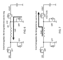
- FIG. 6 illustrates the current flow and voltages in the converter if the “demagnetise” time is too long
- FIG. 7 illustrates the current flow and voltage in the converter if the “demagnetise” time is too short.
- FIG. 8 illustrates a filter that can replace the counter of FIG. 5 to improve stability of the DC to DC converter.
- FIG. 1 shows, in simplified form, a well known configuration of a BUCK-BOOST converter 2 .
- the converter 2 comprises an inductor 4 in combination with first to fourth electrically controlled switches 6 , 8 , 10 and 12 .
- the first switch 6 is connected between an input node 20 and a first node 22 .
- the inductor is connected between the first node 22 and a second node 24 .
- the second switch is connected between the second node 24 and a common node 26 , which typically is a local ground, which in the case of a battery powered device is one of the battery terminals.
- the third switch 10 extends between the common node 26 and the first node 22 .
- the fourth switch is connected between the second node 24 and an output node 30 .
- An energy storage device such as a capacitor 32 , is connected between the output node 30 and the common node 26 so as to store charge for delivery to a load 34 , and also to smooth the voltage at the output node 30 .
- switching converters are well known, but for simplicity it can be regarded as selectively building current in the inductor by placing the first and second switches 6 and 8 into a conducting state while the third and fourth are placed into a non-conducting state. Once the current in the inductor has built to a desired value the first and second switches are made non-conducting and the third and fourth switches are made conducting.
- the magnetic field around the inductor collapses and the energy therein is transferred to the energy storage capacitor 32 .
- the voltage converter has to work over a wide input voltage range.
- the circuit is specified to work for the worst case condition, i.e. lowest permissible input voltage and highest permissible output current.
- the charging current to the inductor is chosen such that peak current is several hundred milliamps.
- the switches are implemented as transistors and each time transistor is switched from non-conducting to conducting it spends a proportion of that time in a regime where the resistance of the transistor is significant enough to give rise to device heating and hence power dissipation—which can be regarded as degrading the conversion efficiency of the DC to DC voltage converter. Energy is also lost charging and discharging parasitic components associated with the control terminal of the transistor. The switching losses are minimal when the converter is supplying a large output current. However, as the output current decreases the switching losses remain substantially unchanged so the proportion of energy lost in the conversion increases.
- FIG. 2 schematically illustrates a pulse skipping mode of operation for the converter topology of FIG. 1 .
- FIG. 2 a shows the coil current, which rises in a first period “ 1 ” when the first and second switches 6 and 8 are closed (conducting) and falls in a second period “ 2 ” when the first and second switches 6 and 8 are non-conducting, but the third and fourth switches are conducting.
- the current in the coil rises and falls cyclically.
- an output current at the output node 30 only has a non-zero value during the time that the magnetic field of the inductor is collapsing.
- magnetization collapsing the field to transfer energy to the capacitor 32 will be referred to as demagnetisation.
- the voltage Vout at the capacitor is monitored, and is allowed to move between an upper voltage threshold V max and a lower voltage threshold V min .
- the converter is arranged that its operation is inhibited once the voltage exceeds V max and is reinstated once the voltage on the capacitor 32 drops below V min . This gives rise to periods labelled “Burst” when the converter is operating and other periods labelled “skip” when the converter is disabled and hence there are no switching losses.
- the skip time can last 100 ms or so whereas the burst time could only be tens of microseconds. Under these circumstances switching losses are reduced by around ten thousand times compared to leaving the converter switching all of the time.
- the inductor may be 2 ⁇ H and V out is 3 V.
- V out is 3 V.
- the offset at the input stage of the comparator needs to be less than 100 ⁇ V.
- the rate of change of coil current is fast, so if we want the comparator to react by the time the discharge current rises by a further 10 mA then the comparator must react around
- parasitic components associated with the real transistor switches can be used to measure the direction of current flow in the coil.
- FIG. 5 shows a DC to DC converter constituting an embodiment of the invention.
- the first to fourth switches 6 , 8 , 10 and 12 are implemented as FETs, and the parasitic diodes D 1 to D 4 associated with the first to fourth switches, 6 , 8 , 10 and 12 , respectively have been shown in the Figure.
- the circuit also includes a first current monitor 50 for detecting when the magnetising current has reached a threshold value. During the magnetization phase current flows into a capacitor C 1 via a series resistor 52 which is connected to input node 20 .
- a shorting switch 54 is in parallel with the capacitor C 1 and is kept in a conducing state until the magnetization sequence is started. As switch 6 closes switch 54 is opened allowing the voltage across the compactor C 1 to build. The voltage across C 1 is compared with a first reference voltage V ref by a comparator 56 . Selection of the relative sizes of C 1 , resistor 52 , and voltage V ref allows the comparator to provide a signal that varies substantially linearly with input voltage V in to indicate when the magnetisation phase is complete. An output of the comparator is provided to a first input of a control circuit 60 which can be as simple as a set-reset flip flop 62 .
- the demagnetise time is measured in the same way as the demagnetise time should also be inversely proportional to V out .
- a shorting switch 76 is provided in parallel with the capacitor C 2 and acts to short the capacitor C 2 out until the demagnetisation phase is started. Once this is commenced the switch is opened a current flowing from the output node via the resistor 72 charges the capacitor C 2 .
- the voltage across C 2 is compared with a second reference voltage V ref by a second comparator 78 who's output is provided to the control circuit 60 .
- resistor 72 and V ref the time taken form the voltage on C 2 to rise to V ref should be substantially inversely proportional to V out .
- Resistors 52 and 72 are typically chosen to have values of several hundred kilo ohm.
- the circuit also includes a mechanism for determining whether the demagnetization time was too long or too short, and means for adjusting the demagnetisation time, although the magnetisation time could be adjusted instead.
- the inventors realised that a short measurement time could be appended to the demagnetisation phase, but prior to the magnetisation phase.
- the first to fourth switches are all placed into their off (non-conducting) state, such that any current flow in the inductor switches the parallel diodes that are inherently formed with the switches into conduction as appropriate for the direction of current flow.
- the diodes are parasitic within an integrated circuit, but can be explicitly provided if desired or if the circuit is built using discrete components.
- a Schmitt trigger 100 has its input connected to node 24 and its output is provided to a direction control pin of an up/down converter 102 .
- the counter receives a clock signal at the end of each measurement period such that it responds to the output of the Schmitt trigger by incrementing or decrementing a control word.
- a latch such as a set-reset latch may be provided intermediate the Schmitt trigger 100 and the counter 102 and reset or set as appropriate just prior to each measurement phase such that it can be used to capture and remember the decision made by the Schmitt trigger (however fleeting) to indicate that demagnetise was too short.
- the capacitor C 2 is implemented as a digitally adjustable capacitor. Thus a plurality of capacitors can be switched into or out of connection to the resistor 72 so as to vary the value of C 2 .
- the number of capacitors is controlled by the output of the counter 102 . Thus if demagnetise was too short, the counter 102 counts up and increases the value of C 2 , thus increasing the duration of the demagnetise time for the next cycle. If demagnetise is too long, the counter counts down, decreasing the length of the demagnetise for the next cycle.
- This feedback loop corrects the value of demagnetise so that it oscillates around its optimum value.
- the feedback mechanism can exhibit a long term oscillatory behaviour because the inductor starts each cycle with a current that corresponds to that of the previous cycle and hence acts as an integrator.
- a second pole is provided is provided by the inductor. It's current is
- the design is also easy to implement.
- the counter 102 can be replaced by a filter implementing this response.
- a filter is illustrated in FIG. 8 and only requires two flip flops to provide the two clock delay elements, a divide by two (which can be done as a shift) and an adder.
Landscapes
- Engineering & Computer Science (AREA)
- Power Engineering (AREA)
- Dc-Dc Converters (AREA)
Abstract
Description
second in this example). Such a fast and accurate comparator would need a lot of bias current and would need a substantial amount of silicon in order to enable it to be trimmed to achieve this level of accuracy. Thus the solution can easily burn more power than would be lost merely by leaving the DC to DC converter running.
and this transforms to the Z domain as
which is unstable, but which can be stabilised by adding a left hand plane zero. If this is also done in the digital domain the transfer function becomes
where Dout(Z) is the digital code used to trim the capacitor and Din(Z) is the value from the Schmitt trigger, i.e. 0 or 1, then for the counter
Claims (32)
Priority Applications (1)
| Application Number | Priority Date | Filing Date | Title |
|---|---|---|---|
| US11/975,305 US7808217B2 (en) | 2007-10-18 | 2007-10-18 | DC to DC converter |
Applications Claiming Priority (1)
| Application Number | Priority Date | Filing Date | Title |
|---|---|---|---|
| US11/975,305 US7808217B2 (en) | 2007-10-18 | 2007-10-18 | DC to DC converter |
Publications (2)
| Publication Number | Publication Date |
|---|---|
| US20090102441A1 US20090102441A1 (en) | 2009-04-23 |
| US7808217B2 true US7808217B2 (en) | 2010-10-05 |
Family
ID=40562826
Family Applications (1)
| Application Number | Title | Priority Date | Filing Date |
|---|---|---|---|
| US11/975,305 Active 2028-10-20 US7808217B2 (en) | 2007-10-18 | 2007-10-18 | DC to DC converter |
Country Status (1)
| Country | Link |
|---|---|
| US (1) | US7808217B2 (en) |
Cited By (8)
| Publication number | Priority date | Publication date | Assignee | Title |
|---|---|---|---|---|
| US20100039086A1 (en) * | 2008-07-07 | 2010-02-18 | Dennis Aan De Stegge | Voltage converter |
| US20100045248A1 (en) * | 2008-08-19 | 2010-02-25 | Advanced Analogic Technologies, Inc. | Bi-directional Boost-Buck Voltage Converter |
| US20100194344A1 (en) * | 2009-02-05 | 2010-08-05 | Infineon Technologies Ag | Combining Two or More DC to DC Converters to Limit External Coils |
| US20100320992A1 (en) * | 2009-06-18 | 2010-12-23 | Micrel, Inc. | Buck-Boost Converter With Sample And Hold Circuit In Current Loop |
| US20110050192A1 (en) * | 2009-08-27 | 2011-03-03 | Richtek Technology Corp. | Methods for light load efficiency improvement of a buck boost voltage regulator |
| US20110086195A1 (en) * | 2006-07-05 | 2011-04-14 | Seagate Technology Llc | Method Of Producing Self-Assembled Cubic FePt Nanoparticles And Apparatus Using Same |
| US20130162171A1 (en) * | 2011-06-03 | 2013-06-27 | Panasonic Corporation | Step up/down converter |
| US20160079790A1 (en) * | 2014-09-12 | 2016-03-17 | Nxp B.V. | Controller for a switched mode power supply and associated methods |
Families Citing this family (10)
| Publication number | Priority date | Publication date | Assignee | Title |
|---|---|---|---|---|
| US7994762B2 (en) * | 2007-12-11 | 2011-08-09 | Analog Devices, Inc. | DC to DC converter |
| EP2515421A1 (en) * | 2009-12-15 | 2012-10-24 | Fujitsu Limited | Power supply device |
| US8446133B2 (en) * | 2010-01-08 | 2013-05-21 | Mediatek Inc. | Methods and control circuits for controlling buck-boost converting circuit to generate regulated output voltage under reduced average inductor current |
| EP2362532A1 (en) * | 2010-02-25 | 2011-08-31 | Dialog Semiconductor GmbH | DC-DC converter efficiency improvement and area reduction using a novel switching technique |
| EP2608357B1 (en) * | 2011-12-19 | 2014-07-23 | Vetco Gray Controls Limited | Protecting against transients in a communication system |
| EP2835900B1 (en) | 2013-08-06 | 2016-10-05 | ams AG | Inductive buck-boost-converter and method for driving an inductive buck-boost-converter |
| EP2897021B1 (en) * | 2014-01-21 | 2020-04-29 | Dialog Semiconductor (UK) Limited | An apparatus and method for a low voltage reference and oscillator |
| CN106208697B (en) * | 2016-08-08 | 2019-03-22 | 成都芯源系统有限公司 | Step-up and step-down switching power converter and control circuit and control method thereof |
| AU2018268716A1 (en) * | 2017-05-15 | 2020-01-16 | Dynapower Company Llc | DC/DC converter and control thereof |
| US10491121B2 (en) * | 2017-10-30 | 2019-11-26 | Renesas Electronics America Inc. | Window comparator structure for low power hysteretic buck-boost DC-DC controller |
Citations (16)
| Publication number | Priority date | Publication date | Assignee | Title |
|---|---|---|---|---|
| US5734258A (en) * | 1996-06-03 | 1998-03-31 | General Electric Company | Bidirectional buck boost converter |
| US5831418A (en) | 1996-12-03 | 1998-11-03 | Fujitsu Ltd. | Step-up/down DC-to-DC converter |
| US6037755A (en) | 1998-07-07 | 2000-03-14 | Lucent Technologies Inc. | Switching controller for a buck+boost converter and method of operation thereof |
| US6087816A (en) * | 1999-06-29 | 2000-07-11 | Maxim Integrated Products, Inc. | Step-up/step-down switching regulators and pulse width modulation control therefor |
| US6166527A (en) | 2000-03-27 | 2000-12-26 | Linear Technology Corporation | Control circuit and method for maintaining high efficiency in a buck-boost switching regulator |
| US6215286B1 (en) * | 1998-11-20 | 2001-04-10 | Texas Instruments Deutschland Gmbh | Step-up/step-down switching regulator operation |
| US6788033B2 (en) * | 2002-08-08 | 2004-09-07 | Vlt, Inc. | Buck-boost DC-DC switching power conversion |
| US6812676B2 (en) | 2002-07-08 | 2004-11-02 | Texas Instruments Incorporated | DC-DC converter and controller for DC-DC converter |
| US6984967B2 (en) | 2003-10-29 | 2006-01-10 | Allegro Microsystems, Inc. | Multi-mode switching regulator |
| US20060176038A1 (en) | 2005-02-08 | 2006-08-10 | Flatness Randy G | Current-mode control for switched step up-step down regulators |
| US7157888B2 (en) | 2005-06-06 | 2007-01-02 | Aimtron Technology Corp. | Light loading control circuit for a buck-boost voltage converter |
| US7176667B2 (en) | 2005-06-20 | 2007-02-13 | Aimtron Technology Corp. | Buck-boost voltage converter |
| US7256570B2 (en) | 2005-02-08 | 2007-08-14 | Linear Technology Corporation | Light load current-mode control for switched step up-step down regulators |
| US7265524B2 (en) | 2004-09-14 | 2007-09-04 | Linear Technology Corporation | Adaptive control for inducer based buck-boost voltage regulators |
| US7298119B1 (en) | 2005-06-03 | 2007-11-20 | Maxim Integrated Products, Inc. | Step-up/step-down (buck/boost) switching regulator control methods |
| US7646179B2 (en) * | 2006-03-20 | 2010-01-12 | Ricoh Company, Ltd. | Electric power supply circuit and electronic device |
-
2007
- 2007-10-18 US US11/975,305 patent/US7808217B2/en active Active
Patent Citations (16)
| Publication number | Priority date | Publication date | Assignee | Title |
|---|---|---|---|---|
| US5734258A (en) * | 1996-06-03 | 1998-03-31 | General Electric Company | Bidirectional buck boost converter |
| US5831418A (en) | 1996-12-03 | 1998-11-03 | Fujitsu Ltd. | Step-up/down DC-to-DC converter |
| US6037755A (en) | 1998-07-07 | 2000-03-14 | Lucent Technologies Inc. | Switching controller for a buck+boost converter and method of operation thereof |
| US6215286B1 (en) * | 1998-11-20 | 2001-04-10 | Texas Instruments Deutschland Gmbh | Step-up/step-down switching regulator operation |
| US6087816A (en) * | 1999-06-29 | 2000-07-11 | Maxim Integrated Products, Inc. | Step-up/step-down switching regulators and pulse width modulation control therefor |
| US6166527A (en) | 2000-03-27 | 2000-12-26 | Linear Technology Corporation | Control circuit and method for maintaining high efficiency in a buck-boost switching regulator |
| US6812676B2 (en) | 2002-07-08 | 2004-11-02 | Texas Instruments Incorporated | DC-DC converter and controller for DC-DC converter |
| US6788033B2 (en) * | 2002-08-08 | 2004-09-07 | Vlt, Inc. | Buck-boost DC-DC switching power conversion |
| US6984967B2 (en) | 2003-10-29 | 2006-01-10 | Allegro Microsystems, Inc. | Multi-mode switching regulator |
| US7265524B2 (en) | 2004-09-14 | 2007-09-04 | Linear Technology Corporation | Adaptive control for inducer based buck-boost voltage regulators |
| US20060176038A1 (en) | 2005-02-08 | 2006-08-10 | Flatness Randy G | Current-mode control for switched step up-step down regulators |
| US7256570B2 (en) | 2005-02-08 | 2007-08-14 | Linear Technology Corporation | Light load current-mode control for switched step up-step down regulators |
| US7298119B1 (en) | 2005-06-03 | 2007-11-20 | Maxim Integrated Products, Inc. | Step-up/step-down (buck/boost) switching regulator control methods |
| US7157888B2 (en) | 2005-06-06 | 2007-01-02 | Aimtron Technology Corp. | Light loading control circuit for a buck-boost voltage converter |
| US7176667B2 (en) | 2005-06-20 | 2007-02-13 | Aimtron Technology Corp. | Buck-boost voltage converter |
| US7646179B2 (en) * | 2006-03-20 | 2010-01-12 | Ricoh Company, Ltd. | Electric power supply circuit and electronic device |
Cited By (15)
| Publication number | Priority date | Publication date | Assignee | Title |
|---|---|---|---|---|
| US20110086195A1 (en) * | 2006-07-05 | 2011-04-14 | Seagate Technology Llc | Method Of Producing Self-Assembled Cubic FePt Nanoparticles And Apparatus Using Same |
| US8383254B2 (en) * | 2006-07-05 | 2013-02-26 | Seagate Technology Llc | Method of producing self-assembled cubic FePt nanoparticles and apparatus using same |
| US8072195B2 (en) * | 2008-07-07 | 2011-12-06 | St-Ericsson Sa | Voltage converter |
| US20100039086A1 (en) * | 2008-07-07 | 2010-02-18 | Dennis Aan De Stegge | Voltage converter |
| US20100045248A1 (en) * | 2008-08-19 | 2010-02-25 | Advanced Analogic Technologies, Inc. | Bi-directional Boost-Buck Voltage Converter |
| US20100194344A1 (en) * | 2009-02-05 | 2010-08-05 | Infineon Technologies Ag | Combining Two or More DC to DC Converters to Limit External Coils |
| US8159181B2 (en) * | 2009-02-05 | 2012-04-17 | Infineon Technologies Ag | Combining two or more DC to DC converters to limit external coils |
| US20100320992A1 (en) * | 2009-06-18 | 2010-12-23 | Micrel, Inc. | Buck-Boost Converter With Sample And Hold Circuit In Current Loop |
| US8085005B2 (en) * | 2009-06-18 | 2011-12-27 | Micrel, Inc. | Buck-boost converter with sample and hold circuit in current loop |
| US20110050192A1 (en) * | 2009-08-27 | 2011-03-03 | Richtek Technology Corp. | Methods for light load efficiency improvement of a buck boost voltage regulator |
| US8547078B2 (en) * | 2009-08-27 | 2013-10-01 | Richtek Technology Corp. | Methods for light load efficiency improvement of a buck boost voltage regulator |
| US20130162171A1 (en) * | 2011-06-03 | 2013-06-27 | Panasonic Corporation | Step up/down converter |
| US8928248B2 (en) * | 2011-06-03 | 2015-01-06 | Panasonic Corporation | Step up/down converter |
| US20160079790A1 (en) * | 2014-09-12 | 2016-03-17 | Nxp B.V. | Controller for a switched mode power supply and associated methods |
| US10003210B2 (en) * | 2014-09-12 | 2018-06-19 | Nxp B.V. | Controller for a switched mode power supply and associated methods |
Also Published As
| Publication number | Publication date |
|---|---|
| US20090102441A1 (en) | 2009-04-23 |
Similar Documents
| Publication | Publication Date | Title |
|---|---|---|
| US7808217B2 (en) | DC to DC converter | |
| US10581328B2 (en) | Synchronous rectifier for buck converter without the need for a comparator | |
| US8179105B2 (en) | Systems and methods for controlling output currents of power converters | |
| EP1579554B1 (en) | Controller for dc to dc converter | |
| US6057675A (en) | DC/DC converter | |
| US7969134B2 (en) | Method of forming a power supply controller and structure therefor | |
| EP1936792B1 (en) | Synchronous rectifier having precise on/off switching times | |
| EP1679780B1 (en) | DC/DC converter with current limit protection | |
| US7161333B2 (en) | System and method for determining load current in switching regulators operable in pulse skipping mode | |
| US9030182B2 (en) | Controller for a DC to DC converter, a combination of a controller and a DC to DC converter, and a method of operating a DC to DC converter | |
| US9479059B2 (en) | Voltage converter for first and second modes of operation | |
| US20140133194A1 (en) | Apparatus and method for detecting a change in output voltage of an isolated power converter | |
| US10693376B2 (en) | Electronic converter and method of operating an electronic converter | |
| US10038385B2 (en) | Flyback converter and controller using counter and current emulator | |
| US7868596B2 (en) | Method of controlling a step-up DC-DC converter and related converter | |
| EP0173697A1 (en) | Flyback switching regulator. | |
| EP1381060A1 (en) | Solenoid drive apparatus and drive method | |
| US20060244429A1 (en) | Free wheeling MOSFET control circuit for pre-biased loads | |
| US9401634B2 (en) | Saturation prevention in an energy transfer element of a power converter | |
| CN111279599A (en) | Timer for power converter controller | |
| US7613017B1 (en) | Gated pulse power converter systems and methods | |
| US6476588B2 (en) | Voltage transformer and associated operating method | |
| US11817773B2 (en) | Systems and methods of adjusting slope compensation | |
| US11233456B2 (en) | Methods and systems of operating power converters | |
| Ko et al. | Load-balance-independent high efficiency single-inductor multiple-output (SIMO) DC-DC converters |
Legal Events
| Date | Code | Title | Description |
|---|---|---|---|
| AS | Assignment |
Owner name: ANALOG DEVICES, INC., MASSACHUSETTS Free format text: ASSIGNMENT OF ASSIGNORS INTEREST;ASSIGNORS:DE CREMOUX, GUILLAUME;GRAY, INNES J.A.;REEL/FRAME:020044/0152 Effective date: 20071012 |
|
| STCF | Information on status: patent grant |
Free format text: PATENTED CASE |
|
| FPAY | Fee payment |
Year of fee payment: 4 |
|
| MAFP | Maintenance fee payment |
Free format text: PAYMENT OF MAINTENANCE FEE, 8TH YEAR, LARGE ENTITY (ORIGINAL EVENT CODE: M1552) Year of fee payment: 8 |
|
| MAFP | Maintenance fee payment |
Free format text: PAYMENT OF MAINTENANCE FEE, 12TH YEAR, LARGE ENTITY (ORIGINAL EVENT CODE: M1553); ENTITY STATUS OF PATENT OWNER: LARGE ENTITY Year of fee payment: 12 |