EP3624172A1 - Method for producing semiconductor device and intermediate for semiconductor device - Google Patents
Method for producing semiconductor device and intermediate for semiconductor device Download PDFInfo
- Publication number
- EP3624172A1 EP3624172A1 EP18797739.2A EP18797739A EP3624172A1 EP 3624172 A1 EP3624172 A1 EP 3624172A1 EP 18797739 A EP18797739 A EP 18797739A EP 3624172 A1 EP3624172 A1 EP 3624172A1
- Authority
- EP
- European Patent Office
- Prior art keywords
- sealing
- semiconductor chips
- semiconductor
- supporting substrate
- producing
- Prior art date
- Legal status (The legal status is an assumption and is not a legal conclusion. Google has not performed a legal analysis and makes no representation as to the accuracy of the status listed.)
- Pending
Links
Images


Classifications
-
- H—ELECTRICITY
- H10—SEMICONDUCTOR DEVICES; ELECTRIC SOLID-STATE DEVICES NOT OTHERWISE PROVIDED FOR
- H10W—GENERIC PACKAGES, INTERCONNECTIONS, CONNECTORS OR OTHER CONSTRUCTIONAL DETAILS OF DEVICES COVERED BY CLASS H10
- H10W74/00—Encapsulations, e.g. protective coatings
- H10W74/01—Manufacture or treatment
- H10W74/019—Manufacture or treatment using temporary auxiliary substrates
-
- H—ELECTRICITY
- H10—SEMICONDUCTOR DEVICES; ELECTRIC SOLID-STATE DEVICES NOT OTHERWISE PROVIDED FOR
- H10W—GENERIC PACKAGES, INTERCONNECTIONS, CONNECTORS OR OTHER CONSTRUCTIONAL DETAILS OF DEVICES COVERED BY CLASS H10
- H10W42/00—Arrangements for protection of devices
- H10W42/20—Arrangements for protection of devices protecting against electromagnetic or particle radiation, e.g. light, X-rays, gamma-rays or electrons
- H10W42/261—Arrangements for protection of devices protecting against electromagnetic or particle radiation, e.g. light, X-rays, gamma-rays or electrons characterised by their shapes or dispositions
- H10W42/276—Arrangements for protection of devices protecting against electromagnetic or particle radiation, e.g. light, X-rays, gamma-rays or electrons characterised by their shapes or dispositions the arrangements being on an external surface of the package, e.g. on the outer surface of an encapsulation
-
- H—ELECTRICITY
- H10—SEMICONDUCTOR DEVICES; ELECTRIC SOLID-STATE DEVICES NOT OTHERWISE PROVIDED FOR
- H10W—GENERIC PACKAGES, INTERCONNECTIONS, CONNECTORS OR OTHER CONSTRUCTIONAL DETAILS OF DEVICES COVERED BY CLASS H10
- H10W70/00—Package substrates; Interposers; Redistribution layers [RDL]
- H10W70/60—Insulating or insulated package substrates; Interposers; Redistribution layers
-
- H—ELECTRICITY
- H10—SEMICONDUCTOR DEVICES; ELECTRIC SOLID-STATE DEVICES NOT OTHERWISE PROVIDED FOR
- H10W—GENERIC PACKAGES, INTERCONNECTIONS, CONNECTORS OR OTHER CONSTRUCTIONAL DETAILS OF DEVICES COVERED BY CLASS H10
- H10W74/00—Encapsulations, e.g. protective coatings
- H10W74/01—Manufacture or treatment
-
- H—ELECTRICITY
- H10—SEMICONDUCTOR DEVICES; ELECTRIC SOLID-STATE DEVICES NOT OTHERWISE PROVIDED FOR
- H10W—GENERIC PACKAGES, INTERCONNECTIONS, CONNECTORS OR OTHER CONSTRUCTIONAL DETAILS OF DEVICES COVERED BY CLASS H10
- H10W74/00—Encapsulations, e.g. protective coatings
- H10W74/01—Manufacture or treatment
- H10W74/014—Manufacture or treatment using batch processing
-
- H—ELECTRICITY
- H10—SEMICONDUCTOR DEVICES; ELECTRIC SOLID-STATE DEVICES NOT OTHERWISE PROVIDED FOR
- H10W—GENERIC PACKAGES, INTERCONNECTIONS, CONNECTORS OR OTHER CONSTRUCTIONAL DETAILS OF DEVICES COVERED BY CLASS H10
- H10W74/00—Encapsulations, e.g. protective coatings
- H10W74/40—Encapsulations, e.g. protective coatings characterised by their materials
- H10W74/47—Encapsulations, e.g. protective coatings characterised by their materials comprising organic materials, e.g. plastics or resins
-
- H—ELECTRICITY
- H10—SEMICONDUCTOR DEVICES; ELECTRIC SOLID-STATE DEVICES NOT OTHERWISE PROVIDED FOR
- H10W—GENERIC PACKAGES, INTERCONNECTIONS, CONNECTORS OR OTHER CONSTRUCTIONAL DETAILS OF DEVICES COVERED BY CLASS H10
- H10W42/00—Arrangements for protection of devices
- H10W42/121—Arrangements for protection of devices protecting against mechanical damage
-
- H—ELECTRICITY
- H10—SEMICONDUCTOR DEVICES; ELECTRIC SOLID-STATE DEVICES NOT OTHERWISE PROVIDED FOR
- H10W—GENERIC PACKAGES, INTERCONNECTIONS, CONNECTORS OR OTHER CONSTRUCTIONAL DETAILS OF DEVICES COVERED BY CLASS H10
- H10W42/00—Arrangements for protection of devices
- H10W42/20—Arrangements for protection of devices protecting against electromagnetic or particle radiation, e.g. light, X-rays, gamma-rays or electrons
-
- H—ELECTRICITY
- H10—SEMICONDUCTOR DEVICES; ELECTRIC SOLID-STATE DEVICES NOT OTHERWISE PROVIDED FOR
- H10W—GENERIC PACKAGES, INTERCONNECTIONS, CONNECTORS OR OTHER CONSTRUCTIONAL DETAILS OF DEVICES COVERED BY CLASS H10
- H10W70/00—Package substrates; Interposers; Redistribution layers [RDL]
- H10W70/01—Manufacture or treatment
- H10W70/05—Manufacture or treatment of insulating or insulated package substrates, or of interposers, or of redistribution layers
- H10W70/08—Manufacture or treatment of insulating or insulated package substrates, or of interposers, or of redistribution layers by depositing layers on the chip or wafer, e.g. "chip-first" RDLs
- H10W70/09—Manufacture or treatment of insulating or insulated package substrates, or of interposers, or of redistribution layers by depositing layers on the chip or wafer, e.g. "chip-first" RDLs extending onto an encapsulation that laterally surrounds the chip or wafer, e.g. fan-out wafer level package [FOWLP] RDLs
-
- H—ELECTRICITY
- H10—SEMICONDUCTOR DEVICES; ELECTRIC SOLID-STATE DEVICES NOT OTHERWISE PROVIDED FOR
- H10W—GENERIC PACKAGES, INTERCONNECTIONS, CONNECTORS OR OTHER CONSTRUCTIONAL DETAILS OF DEVICES COVERED BY CLASS H10
- H10W72/00—Interconnections or connectors in packages
- H10W72/01—Manufacture or treatment
- H10W72/0198—Manufacture or treatment batch processes
-
- H—ELECTRICITY
- H10—SEMICONDUCTOR DEVICES; ELECTRIC SOLID-STATE DEVICES NOT OTHERWISE PROVIDED FOR
- H10W—GENERIC PACKAGES, INTERCONNECTIONS, CONNECTORS OR OTHER CONSTRUCTIONAL DETAILS OF DEVICES COVERED BY CLASS H10
- H10W72/00—Interconnections or connectors in packages
- H10W72/20—Bump connectors, e.g. solder bumps or copper pillars; Dummy bumps; Thermal bumps
- H10W72/241—Dispositions, e.g. layouts
-
- H—ELECTRICITY
- H10—SEMICONDUCTOR DEVICES; ELECTRIC SOLID-STATE DEVICES NOT OTHERWISE PROVIDED FOR
- H10W—GENERIC PACKAGES, INTERCONNECTIONS, CONNECTORS OR OTHER CONSTRUCTIONAL DETAILS OF DEVICES COVERED BY CLASS H10
- H10W74/00—Encapsulations, e.g. protective coatings
- H10W74/10—Encapsulations, e.g. protective coatings characterised by their shape or disposition
- H10W74/111—Encapsulations, e.g. protective coatings characterised by their shape or disposition the semiconductor body being completely enclosed
- H10W74/114—Encapsulations, e.g. protective coatings characterised by their shape or disposition the semiconductor body being completely enclosed by a substrate and the encapsulations
- H10W74/117—Encapsulations, e.g. protective coatings characterised by their shape or disposition the semiconductor body being completely enclosed by a substrate and the encapsulations the substrate having spherical bumps for external connection
Definitions
- the present invention relates to a method for producing a semiconductor apparatus and an intermediate of the semiconductor apparatus.
- semiconductor devices such as an IC using a silicon semiconductor or an organic EL device using an organic semiconductor are generally produced by forming many devices on a wafer substrate surface in a matrix form and then dividing the devices into individual devices by dicing.
- the semiconductor chips are packaged by being applied with resin sealing and the like, and are mounted on various electronic devices.
- a technology called fan-out wafer-level packaging is proposed (for example, see Patent Literature (hereinafter, abbreviated as PTL) 1).
- PTL Patent Literature
- a rear surface side (a side opposite to the circuit surface) of the semiconductor chip is sealed with resin.
- a re-distribution layer is formed on a front surface (circuit surface) of the semiconductor chip, and an external terminal is further formed on the re-distribution layer.
- a large-area packaging technology is needed in terms of cost reduction.
- collective sealing of a plurality of semiconductor chips and collective formation of an RDL (re-distribution layer) in a large area that is a high-cost process are needed.
- PTL 1 discloses a method for producing a semiconductor apparatus through (1) a step of fixing a plurality of semiconductor chips on a supporting substrate so that front surfaces (circuit surfaces) thereof face down; (2) a step of collectively sealing rear surfaces of the plurality of semiconductor chips with a sealing material; (3) a step of obtaining a sealed body by removing the supporting substrate; (4) a step of forming re-distribution layers on front surfaces (circuit surfaces) of the semiconductor chips of the sealed body that are exposed, and further forming external connection terminals such as metal bumps thereon; and (5) a step of dividing the semiconductor chips into individual semiconductor chips or packages each formed from a plurality of semiconductor chips.
- the sealing resin is formed on the entire surface of the supporting substrate including places between the plurality of semiconductor chips.
- the contact area between the sealing material and the supporting substrate is large, and hence there has been a problem in that a warp is easily generated in the sealed body and misalignment (die shift) of the semiconductor chips easily occur due to the difference in the coefficient of thermal expansion between the sealing material and the supporting substrate at the time of sealing and when the supporting substrate is removed.
- the present invention has been made in view of the abovementioned situation, and an object thereof is to provide a method for producing a semiconductor apparatus and an intermediate of the semiconductor apparatus that may suppress a warp in a sealed body and misalignment of a plurality of semiconductor chips when the sealed body is obtained by collectively sealing the semiconductor chips, and suppress the reduction of the handleability of the sealed body and the reliability of the semiconductor apparatus after the sealed body is obtained.
- the present invention relates to the following method for manufacturing a semiconductor apparatus and also to an intermediate of a semiconductor apparatus.
- the method for producing the semiconductor apparatus that may suppress the warp in the sealed body and the misalignment of the semiconductor chips when the sealed body is obtained by collectively sealing the semiconductor chips, and suppress the reduction of the handleability of the sealed body and the reliability of the semiconductor apparatus after the sealed body is obtained can be provided.
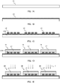
- FIGS. 1A to 1I illustrate an example of a method for producing a semiconductor apparatus according to an embodiment of the present invention.
- the method for producing the semiconductor apparatus according to this embodiment includes a first step of fixing plurality of semiconductor chips 13 on supporting substrate 11; a second step of applying sealing material 17 to plurality of semiconductor chips 13, and forming plurality of sealing layers 19, each sealing layer 19 containing one or more semiconductor chips 13 covered with sealing material 17; a third step of curing or solidifying sealing layers 19; and a fourth step of obtaining sealed bodies 21 by removing cured or solidified sealing layers 19 from supporting substrate 11.
- the method for producing the semiconductor apparatus may further include, as necessary, one or more other steps out of a step of forming re-distribution layer 23 on a surface of each obtained sealed body 21 on which one or more semiconductor chips are exposed, a step of forming bumps 25 on re-distribution layer 23, a step of forming ground wire on the outer peripheries of semiconductor chips 13 of obtained sealed body 21, and a step of forming an electromagnetic wave shield layer on a surface of obtained sealed body 21 on which one or more semiconductor chips 13 are not exposed.
- the order of the other steps is not particularly limited.
- a method for producing a semiconductor apparatus by successively forming the re-distribution layer or an external terminal on a circuit surface of the semiconductor chip, as necessary, after sealing the side of semiconductor chip opposite to the circuit surface by resin is also referred to as a fan-out wafer-level packaging method.
- supporting substrate 11 is prepared (see FIG. 1A ).
- supporting substrate 11 include glass substrates such as a quartz substrate and an alkali-free glass substrate, metal plates such as an SUS substrate, wafer substrates such as a silicon wafer, a SiC wafer, and a GaAs wafer, and resin substrates.
- the linear expansion coefficient is preferred to be low, and the glass substrates and the SUS substrate are preferred.
- the thickness of supporting substrate 11 is not particularly limited, but may be 10 ⁇ m to 20 mm, for example, in terms of reducing the warp and the deformation of sealed bodies 21 even more and increasing the handleability.
- the thickness of supporting substrate 11 is 10 ⁇ m or more, the warp and the deformation of sealed bodies 21 is much less likely to be generated in the production step, and conveyance trouble during the production step is less likely to occur, and hence productivity decline due to the decrease in the yield rate is less likely to occur.
- the thickness of supporting substrate 11 is 20 mm or less, the weight does not become too heavy, and hence the conveyance is less likely to become difficult and excellent handleability is provided.
- the size of supporting substrate 11 is not particularly limited, but the maximum width is preferred to be 5 cm to 50 cm, more preferred to be 10 cm to 30 cm (12 inches), and further preferred to be 10 cm to 20 cm (8 inches) in terms of reducing the warp and the deformation of sealed bodies 21 even more and improving the yield.
- plurality of semiconductor chips 13 are fixed on supporting substrate 11 so that front surfaces 13A (circuit surfaces) thereof are on supporting substrate 11 side.
- the method for fixing plurality of semiconductor chips 13 is not particularly limited, but can be performed, for example, by disposing adhesive sheet 15 on supporting substrate 11, and then further disposing plurality of semiconductor chips 13 on adhesive sheet 15 (see FIGS. 1B to 1C ).
- Examples of adhesive sheet 15 include a photocurable adhesive sheet that is cured and adhesive force thereof decreases by being irradiated with light, and a thermally-expandable adhesive sheet, which thermally expands and adhesive force thereof decreases by heating.
- Sealing material 17 containing a sealing resin is applied to rear surfaces 13B (surfaces on a side opposite to the circuit surfaces) of plurality of semiconductor chips 13 fixed on supporting substrate 11. As a result, plurality of sealing layers 19 are formed on supporting substrate 11 at intervals, and each sealing layer 19 contains one or more semiconductor chips 13 covered with sealing material 17.
- FIGS. 2A and 2B illustrate an example of a step of forming plurality of sealing layers 19.
- FIG. 2A is a plan view
- FIG. 2B is a cross-sectional view.
- plurality of sealing layers 19 are formed on supporting substrate 11 at intervals.
- the contact area between supporting substrate 11 and each sealing layer 19 can be small, and hence the warp in sealed bodies 21 and the misalignment of semiconductor chips 13 due to the difference in the coefficient of linear expansion between supporting substrate 11 and sealing layers 19 (or sealing material 17) can be reduced.
- the shape of sealing layer 19 is not particularly limited, and may be a rectangular shape or a circular shape, and is preferred to be a rectangular shape in terms of increasing the yield.
- the misalignment of semiconductor chips 13 and the warp in sealed bodies 21 due to the difference in the coefficient of linear expansion between sealing layers 19 and supporting substrate 11 is proportional to the contact area between one continuous sealing layer 19 and supporting substrate 11.
- sealing material 17 includes "a thermosetting resin that causes (sealing layers 19) ⁇ (supporting substrate 11) to be satisfied in terms of the coefficient of linear expansion" as the sealing resin, the misalignment of semiconductor chips 13 easily occur and the warp is easily generated in sealed bodies 21 due to the difference in the shrinkage rate (the difference in the coefficient of linear expansion) between sealing layers 19 and supporting substrate 11 in a cooling process when sealing material 17 is cooled after being applied and cured by heating.
- the shrinkage rate of supporting substrate 11 is larger than the shrinkage rate of sealing layers 19, the interval between adjacent sealing layers 19 is narrowed in the cooling process, thereby causing a fear of contact between adjacent sealing layers 19.
- sealing material 17 includes "a thermosetting resin or a photocurable resin that causes (sealing layers 19)>(supporting substrate 11) to be satisfied in terms of the coefficient of linear expansion" as the sealing resin, the misalignment of semiconductor chips 13 easily occur and the warp is easily generated in sealed bodies 21 due to the difference in the expansion rate (the difference in the coefficient of linear expansion) between sealing layers 19 and supporting substrate 11 in the process of heating sealing material 17 after applying and curing sealing material 17.
- the expansion rate of supporting substrate 11 is smaller than the expansion rate of sealing layer 19, the interval between adjacent sealing layers 19 is narrowed in the heating process after the curing, thereby causing a fear of contact between adjacent sealing layers 19.
- the percentage of minimum width d of the interval between sealing layer 19 and sealing layer 19 that are adjacent to each other in plan view with respect to maximum width W of sealing layer 19 ((minimum width d of the interval between sealing layer 19 and sealing layer 19)/(maximum width W of sealing layer 19) ⁇ 100 (%)) is preferred to be 0.19% to 10% of maximum width W of sealing layer 19.
- d/W ⁇ 100 the contact between adjacent sealing layers 19 caused by interval d between adjacent sealing layers 19 being narrowed can be suppressed to a high degree.
- the abovementioned numeric range can be obtained with use of analysis software ANSYS and the like.
- the maximum value of the moving distance of semiconductor chips 13 in the cooling process after the heating and curing or the heating process after the curing when the materials of supporting substrate 11, semiconductor chips 13, and sealing layers 19 are combined in a predetermined manner is calculated with use of analysis software ANSYS.
- a value exceeding the obtained maximum value of the moving distance of semiconductor chips 13 is set as the minimum value of interval d between adjacent sealing layers 19, and is divided by maximum width W of sealing layer 19, to thereby compute the abovementioned percentage (d/W ⁇ 100).
- the operation can be performed by changing the combination of the materials, and the minimum value out of the obtained percentages (d/W ⁇ 100) can be set as the lower limit value of the abovementioned percentage (d/W ⁇ 100).
- supporting substrate 11 be at least one type selected from an SUS substrate, a glass substrate, and a silicon wafer
- sealing layers 19 contain at least one type from a thermosetting resin and a photocurable resin
- supporting substrate 11 be an SUS substrate and sealing layers 19 contain an epoxy resin.
- Maximum width W of sealing layer 19 differs according to the size of semiconductor chip 13, the producing apparatus, and the like, and is not particularly limited, but is preferred to be 10 mm to 60 mm, for example.
- maximum width W of sealing layer 19 is 10 mm or more, a sufficient number of semiconductor chips 13 are easily disposed on one sealing layer 19.
- maximum width W of sealing layer 19 is 60 mm or less, the contact area between one sealing layer 19 and supporting substrate 11 may be sufficiently reduced. Therefore, the warp in sealed bodies 21 and the misalignment of semiconductor chips 13 are sufficiently suppressed in an easy manner.
- Minimum value d of the interval between sealing layer 19 and sealing layer 19 that are adjacent to each other is not particularly limited as long as the abovementioned percentage (d/W ⁇ 100) is satisfied, but is preferred to be 0.18 mm to 6.0 mm, and more preferred to be 0.5 mm to 3.0 mm, for example.
- minimum value d is within the abovementioned range, the suppression of the warp in sealed bodies 21 and the misalignment of semiconductor chips 13 and the yield of semiconductor chips 13 may be both achieved to a high degree.
- Thickness t1 of sealing layer 19 only needs to be a thickness with which entire semiconductor chip 13 can be embedded after the curing or solidifying, and may be set so that the thickness after the curing or solidifying reaches about 0.1 mm to about 5 mm, for example (see FIG. 2B ).
- the absolute value of the difference in the coefficient of linear expansion between supporting substrate 11 and sealing material 17 is preferred to be 15 ppm/K or less, and is more preferred to be 9.3 ppm/K or less in terms of causing the misalignment of semiconductor chips 13 and the warp in sealed bodies 21 to be easily suppressed.
- the number of semiconductor chips 13 included in one sealing layer 19 is preferred to be small in terms of suppressing the misalignment of semiconductor chips 13 and the warp in sealed bodies more by reducing the area of one continuous sealing layer 19. Specifically, the number of semiconductor chips 13 included in one sealing layer 19 is preferred to be one to ten, more preferred to be one to three, and particularly preferred to be one.
- sealing layers 19, that is, the application of sealing material 17 is performed from a three-dimensional molding method.
- heat is less likely to be generated when sealing, curing, or solidifying are performed unlike a mold molding method such as transfer molding of the related art.
- the warp due to the difference in the coefficient of thermal expansion between supporting substrate 11 and sealing layers 19 may be suppressed, and the misalignment of semiconductor chips 13 may be suppressed.
- the three-dimensional molding method is not particularly limited, but may be any of a stereo lithography method (STL method), a material jetting method (ink-jet method), a fused deposition modeling method (FDM method), and a selective laser sintering method (SLS method).
- STL method stereo lithography method
- FDM method fused deposition modeling method
- SLS method selective laser sintering method
- the stereo lithography method is a method of forming and depositing a resin layer on supporting substrate 11 on which plurality of semiconductor chips 13 are fixed that is disposed on a molding stage in a tank filled with a liquid photocurable resin composition by irradiating only a desired portion of a liquid surface of the tank with light.
- the material jetting method is a method of forming and depositing a resin layer by jetting out a liquid photocurable resin composition or thermosetting resin composition and curing the liquid photocurable resin composition that has been jetted out by irradiating the liquid photocurable resin composition that has been jetted out with light or curing the liquid thermosetting resin composition that has been jetted out by heating.
- the fused deposition modeling method is a method of forming and depositing a resin layer by pushing out a thermoplastic resin composition melted by heat from a head (nozzle) and then cooling the thermoplastic resin composition.
- the selective laser sintering method is a method of forming and depositing a resin layer by jetting out thermoplastic resin powder and then sintering (fusing) the thermoplastic resin powder by a laser.
- the material jetting method ink-jet method
- the fused deposition modeling method FDM method
- Sealing material 17 to be used may be selected in accordance with the type of the three-dimensional molding method.
- Sealing material 17 may be a curable resin composition containing a curable resin as the sealing resin, or may be a thermoplastic resin composition containing a thermoplastic resin as the sealing resin.
- the curable resin composition may be a photocurable resin composition or may be a thermosetting resin composition.
- the photocurable resin composition includes a curing agent and a photocurable resin as the sealing resin.
- the photocurable resin include photo-radical curable compounds such as a (meth)acrylic ester compound, and photo-cationic curable compounds such as an epoxy resin.
- the curing agent of the photo-radical curable compound include photo-radical initiators such as a benzoin compound, an acylphosphine-oxide compound, and benzophenone compound, and acetophenones.
- Examples of the curing agent of the photo-cationic curable compound include photo-cationic initiators such as a photoacid generator.
- thermosetting resin composition contains a curing agent and a thermosetting resin as the sealing resin.
- thermosetting resin include an epoxy resin.
- curing agent of the thermosetting resin include acid anhydrides, an amine compound, and a phenolic compound.
- the thermoplastic resin composition contains a thermoplastic resin as the sealing resin.
- the thermoplastic resin include polylactic acid (PLA resin), an acrylonitrile-butadiene-styrene copolymer (ABS resin), polyolefin, polyester, polyamide, polyimide, polyether ketone, polybenzoxazole, and an acrylic resin.
- Sealing material 17 is preferred to be a thermosetting resin composition or a photocurable resin composition in terms of mechanical strength, heat resistance, water vapor permeability, and the like.
- the thermosetting resin used in the thermosetting resin composition or the photocurable resin used in the photocurable resin composition is preferred to be at least one type selected from a group consisting of an epoxy resin, a polyimide resin, and a urea resin.
- sealing material 17 is preferred to be a photocurable resin composition or a thermoplastic resin composition in terms of causing heat to be less likely to be generated during the sealing.
- the photocurable resin composition, the thermosetting resin composition, and the thermoplastic resin composition may each further include an insulating filling agent such as a ceramic filler and an inorganic filler, as necessary, in terms of suppressing the warp in obtained sealed bodies 21 even more and improving the reliability and the yield of semiconductor package 27 or 27' (see FIGS. 1H and 1I ) even more, for example, by increasing the heat resistance and reducing the coefficient of linear expansion of sealing layer 19 after the curing or solidifying.
- an insulating filling agent such as a ceramic filler and an inorganic filler
- sealing material 17 may further contain a filling agent.
- the content percentage of the filling agent in sealing material 17 is preferred to be 10mass% or less, more preferred to be 5mass% or less, and further preferred to be 1mass% or less with respect to the total mass of sealing material 17 in terms of easily suppressing the clogging in the apparatus and preventing the ejection property from being impaired when sealing material 17 is applied to semiconductor chips 13 in the three-dimensional molding method.
- the filling agent examples include silicate such as talc, baked clay, unbaked clay, mica, and glass, oxide such as titanium oxide, alumina, fused silica (fused spherical silica, fractured fused silica), and crystalline silica powder, carbonate such as calcium carbonate, magnesium carbonate, and hydrotalcite, hydroxides such as aluminum hydroxide, magnesium hydroxide, and calcium hydroxide, sulfate or sulfite such as barium sulfate, calcium sulfate, and calcium sulfite, borate such as zinc borate, barium metaborate, aluminum borate, calcium borate, and sodium borate, and nitride such as aluminum nitride, boron nitride, and silicon nitride.
- silicate such as talc, baked clay, unbaked clay, mica, and glass
- oxide such as titanium oxide, alumina
- fused silica fused silica (fused sp
- sealing resin contained in sealing material 17 be an epoxy resin and the content percentage of the filling agent (filler) be 10mass% or less with respect to the total mass of sealing material 17, and it is more preferred that the sealing resin be an epoxy resin and the content percentage of the filling agent (filler) be 5mass% or less with respect to the total mass of sealing material 17.
- the coefficient of viscosity of sealing material 17 when sealing material 17 is ejected from the apparatus in the three-dimensional molding method is preferred to be 1 mPa ⁇ s to 20 mPa ⁇ s.
- the coefficient of viscosity of sealing material 17 is in the abovementioned range, the clogging of the apparatus in the three-dimensional molding method is easily suppressed, and hence the ejection property easily becomes satisfactory and sealing layer 19 is easily formed in a desired shape.
- Obtained sealing layers 19 are cured or solidified (see FIG. IE).
- Sealing layers 19 may be cured by photo-curing or thermal curing. In other words, when sealing layers 19 are formed from a photocurable resin composition, sealing layers 19 are irradiated with light, to thereby be cured (see FIG. IE). When sealing layers 19 are formed from a thermosetting resin composition, sealing layers 19 are heated, to thereby be cured.
- Sealing layers 19 may be solidified by solidifying by cooling. In other words, when sealing layers 19 are formed from a thermoplastic resin composition, sealing layers 19 are solidified by cooling.
- the glass transition temperature of sealing layers 19 after the curing or solidifying is preferred to be 110°C or more, more preferred to be 150°C or more, and further preferred to be 200°C or more.
- the glass transition temperature can be measured by a method below.
- a test piece formed of cured or solidified sealing material 17 with a width of 4 mm and a length of 20 mm is prepared.
- TMA measurement of the glass transition temperature of the test piece is performed with use of a thermomechanical analyzer (TMA-50) made by Shimadzu Corporation with the measurement condition of a temperature range from 25°C to 350°C, a temperature rising rate of 5°C/minute, a load of 14 g/mm2, and a tension mode.
- TMA-50 thermomechanical analyzer
- the glass transition temperature (Tg) can be specified from the inflection point of the obtained temperature-test piece elongation curve.
- the glass transition temperature of sealing layer 19 after the curing or solidifying can be mainly adjusted by the composition of sealing material 17.
- the curable resin composition be selected as sealing material 17 or the filling agent (filler) be added.
- the content percentage of the filling agent in sealing layers 19 is preferred to be 50mass% to 95mass%, and more preferred to be from 60mass% to 90mass% with respect to the total mass of sealing layer 19.
- the contained amount of the filling agent is within the abovementioned range, the deterioration of semiconductor chips 13 due to moisture in the atmosphere is suppressed to a high degree and the generation of cracks is easily suppressed.
- sealing layers 19 containing the filling agent may be formed by applying sealing material 17 containing the filling agent by a three-dimensional molding method, or may be formed by applying the filling agent around semiconductor chips 13 in advance and further applying sealing material 17 that does not contain the filling agent thereon.
- each sealing layer 19 containing one or more semiconductor chips 13 embedded in sealing material 17 is obtained.
- Sealed bodies 21 are obtained by removing cured or solidified sealing layers 19 of the obtained intermediate from supporting substrate 11 (see FIG. IF).
- the method for removing cured or solidified sealing layers 19 from supporting substrate 11 is not particularly limited.
- adhesive sheet 15 is a photocurable adhesive sheet
- cured or solidified sealing layers 19 are removed by reducing the adhesive force by irradiating adhesive sheet 15 with light (see FIG. IF).
- adhesive sheet 15 is a thermally-expandable adhesive sheet
- cured or solidified sealing layers 19 are removed by reducing the adhesive force by heating adhesive sheet 15.
- Obtained sealed body 21 includes one or more semiconductor chips 13, and a layer formed of cured or solidified sealing material 17' in which the entirety of one or more semiconductor chips 13 except for front surfaces 13A thereof are embedded.
- Re-distribution layer 23 may be formed on a surface of obtained sealed body 21 on which one or more semiconductor chips 13 are exposed (a step of forming re-distribution layer 23, see FIG. 1G ).
- Re-distribution layer 23 includes a rewiring portion (not shown) and a rewiring insulating layer (not shown).
- the material of the rewiring portion may be a metal material generally used for wiring, and examples thereof include copper and aluminum.
- the material of the rewiring insulating layer may be resins such as an epoxy resin, polyolefin, an acrylic resin, polyester, an ABS resin, polyimide, polyether ketone, and polybenzoxazole.
- resins such as an epoxy resin, polyolefin, an acrylic resin, polyester, an ABS resin, polyimide, polyether ketone, and polybenzoxazole.
- a curable resin whose glass transition temperature after the curing is 110°C or more, preferably 150°C or more, more preferably 200°C or more is preferred, and examples thereof include an epoxy resin, thermosetting polyolefin, polyimide, polyether ketone, and polybenzoxazole.
- the glass transition temperature of the cured product of the curable resin can be measured by a method similar to that for the glass transition temperature of cured or solidified sealing layers 19.
- the rewiring insulating layer may further include an insulating filling material such as a ceramic filler and an inorganic filler, as necessary, in terms of suppressing the warp of semiconductor package 27 or 27' (see FIGS. 1H and FIG. 1I ) and improving the reliability and the yield of semiconductor package 27 or 27' by increasing the heat resistance and reducing the coefficient of linear expansion, and in terms of reducing the permittivity of the material and reducing transmission loss.
- an insulating filling material such as a ceramic filler and an inorganic filler
- the method for forming re-distribution layer 23 is not particularly limited, and may be a semi-additive method, a subtractive method, a three-dimensional molding method, or the like. Among the above, the three-dimensional molding method is preferred.
- the generation of heat when re-distribution layer 23 is formed can be reduced, and hence the warp in sealed bodies 21 and the misalignment of semiconductor chips 13 may be suppressed even more.
- the formation of detailed wiring that has been difficult to form becomes possible, and the designs of sealed bodies 21 are easily changed, as necessary, for each sealed body 21.
- the wiring portion can be formed from a material jetting method (ink-jet method) using a metallic paste such as a copper paste, and a selective metal laser sintering method (SLS method) using metal microparticles of gold, silver, copper, nickel, and the like.
- a material jetting method ink-jet method
- a metallic paste such as a copper paste
- SLS method selective metal laser sintering method
- a step of forming bumps 25 on the surface of obtained sealed body 21 on which one or more semiconductor chips 13 are exposed or re-distribution layer 23 may be further performed (a step of forming bumps 25, see FIG. 1H ).
- the material of the bumps may be a well-known metal material generally used for bumps.
- a step of forming ground wire (not shown) on the surface of obtained sealed body 21 on which one or more semiconductor chips 13 are exposed so that the ground wire is formed on the outer peripheries of one or more semiconductor chips 13 may be further performed (a step of forming ground wire, not shown).
- the material of the ground wire may be a well-known metal material generally used for wiring, and examples thereof include copper and aluminum.
- the method for forming the ground wire is not particularly limited, but is preferred to be a three-dimensional molding method because the generation of heat when the wiring is formed can be reduced and detailed wiring can be formed.
- the ground wire can be formed from a material jetting method (ink-jet method) using a metallic paste such as a copper paste, and a selective metal laser sintering method (SLS method) using metal microparticles of gold, silver, copper, nickel, and the like.
- a step of forming an electromagnetic wave shield layer (not shown) on at least one portion of a surface of obtained sealed body 21 on which one or more semiconductor chips 13 are not exposed may be further performed (a step of forming an electromagnetic wave shield layer, not shown).
- the material of the electromagnetic wave shield layer may be a metal material generally used for an electromagnetic wave shield, and examples thereof include silver, copper, gold, aluminum, magnesium, tungsten, cobalt, zinc, nickel, iron, platinum, tin, chromium, lead, titanium, manganese, and stainless steel. Among the above, silver, copper, gold, and aluminum that have low resistivity are preferred.
- the method for forming the electromagnetic wave shield layer is not particularly limited, but is preferred to be a three-dimensional molding method.
- the electromagnetic wave shield layer can be formed from a material jetting method (ink-jet method) using a metallic paste, and a selective metal laser sintering method (SLS method) using a metal microparticle.
- Sealed body 21 obtained as described above may be directly made into semiconductor package 27 (semiconductor apparatus) (see FIG. 1H ), or may be made into semiconductor packages 27' (semiconductor apparatuses) by further dividing sealed body 21 into each of semiconductor chips 13 or each of packages formed from a plurality of semiconductor chips 13 (see FIG. 1I ).
- sealing layers 19 are formed at intervals. As a result, the contact area between each of sealing layers 19 and supporting substrate 11 can be reduced. Sealing layers 19 are formed by the three-dimensional molding method. As a result, the generation of heat when sealing layers 19 are formed can be reduced as compared to the mold molding method of the related art. As a result, the warp in sealed bodies 21 and the misalignment of semiconductor chips 13 (die shift) due to the difference in the coefficient of thermal expansion between supporting substrate 11 and sealing layers 19 can be suppressed.
- one sealing layer 19 seals plurality of semiconductor chips 13 so as to include plurality of semiconductor chips 13 is described in the second step.
- one sealing layer 19 may seal one semiconductor chip 13 so as to include one semiconductor chip 13.
- a frame body is not used.
- the present invention is not limited thereto, and a frame body may be further used.
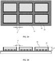
- FIGS. 3A and 3B illustrate another example of a step of forming plurality of sealing layers 19.
- FIG. 3A is a plan view
- FIG. 3B is a cross-sectional view.
- a step of forming frame bodies 29 that surround the outer peripheries of sealing layers 19 may further be performed.
- Frame bodies 29 may be formed before or after the second step.
- frame bodies 29 are preferred to be formed before the second step in terms of easily suppressing the deformation of sealing layers 19 due to heat generated at the time of sealing.
- sealing layers 19 be formed by applying sealing material 17 on the inner side of frame bodies 29 in the second step.
- the method for forming frame bodies 29 may be a method of disposing frame bodies that are molded in advance, or may be a method of directly forming frame bodies 29 on supporting substrate 11 by coating.
- Frame bodies 29 may have a function of suppressing deformation caused by the thermal expansion of sealing layers 19. Frame bodies 29 may also have a function of causing sealing layers 19 to be less likely to stick to each other even when the minimum interval between adjacent sealing layers 19 is small and sealing layers 19 may easily stick to each other by thermal expansion.
- Frame bodies 29 are preferred to include a material whose linear expansion coefficient at the temperature of 60°C to 250°C is 35 ppm/K or less, or a resin whose tensile modulus of elasticity at the temperature of 60°C to 250°C is less than the tensile modulus of elasticity of sealing material 17 after the curing or solidifying by 0.5 GPa or more.
- frame bodies 29 include a material whose linear expansion coefficient is 35 ppm/K or less at the temperature of 60°C to 250°C, the force of sealing layer 19 that is about to thermally expand can be suppressed. As a result, the warp in sealed bodies 21 and the misalignment of semiconductor chips 13 can be suppressed even more.
- the coefficient of linear expansion of the material can be measured by a method below.
- a sample piece (about 30 ⁇ m, length 20 mm) formed of the material to be measured is prepared.
- a thermomechanical analyzer TMA-50, made by Shimadzu Corporation
- a constant load 14 g for 1 mm 2 of the cross section of the film
- the linear expansion coefficient (unit: ppm/K) is measured from the elongation (shrinkage) when the temperature is changed.
- Examples of a material whose linear expansion coefficient at the temperature of 60°C to 250°C is 35 ppm/K or less include metal materials such as aluminum (23 ppm/K), iron (12 ppm/K), tungsten (4.3 ppm/K), chromium (6.8 ppm/K), carbon steel (10.8 ppm/K), stainless steel (10 ppm/K to 17 ppm/K), nickel (12.8 ppm/K), copper (16.8 ppm/K), and magnesium (25.4 ppm/K), and inorganic materials such as Pyrex (R) glass (3.2 ppm/K), silicon carbide (6.6 ppm/K), hard glass (8.5 ppm/K), and silicon (24 ppm/K).
- metal materials such as aluminum (23 ppm/K), iron (12 ppm/K), tungsten (4.3 ppm/K), chromium (6.8 ppm/K), carbon steel (10.8 ppm/K), stainless steel (10 ppm/K to 17 ppm
- frame bodies 29 include a resin whose tensile modulus of elasticity at the temperature of 60°C to 250°C is lower than the tensile modulus of elasticity of the sealing material after the curing or solidifying by 0.5 GPa or more, the force of the thermal expansion of sealing layer 19 can be absorbed and alleviated. As a result, the warp in sealed bodies 21 and the misalignment of semiconductor chips 13 can be suppressed even more.
- the tensile modulus of elasticity of the resin can be measured by a method below.
- a sheet-like test piece with a thickness of 1 mm formed of the resin to be measured is prepared.
- the tensile modulus of elasticity (GPa) of the test piece is measured by a tensile testing apparatus under an atmosphere at a temperature of any of the temperature of 60°C to 250°C and the relative humidity of 50% based on ASTM D638.
- Examples of a resin whose tensile modulus of elasticity at the temperature of 60°C to 250°C is less than the tensile modulus of elasticity of the sealing material after the curing or solidifying by 0.5G Pa or more include elastomers such as butadiene rubber, isoprene rubber, silicon rubber, styrene-butadiene rubber, chloroprene rubber, nitrile rubber, butyl rubber, ethylene-propylene rubber, acrylic rubber, chlorosulfonated polyethylene rubber, fluoro rubber, hydrogenated nitrile rubber, and epichlorohydrin rubber.
- elastomers such as butadiene rubber, isoprene rubber, silicon rubber, styrene-butadiene rubber, chloroprene rubber, nitrile rubber, butyl rubber, ethylene-propylene rubber, acrylic rubber, chlorosulfonated polyethylene rubber, fluoro rubber, hydrogenated nitrile rubber, and epichlorohydr
- Thickness t2 of frame body 29 may be the same as or different from thickness t1 of sealing layer 19, but is preferred to be the same as thickness t1 of sealing layer 19 in terms of improving the handleability and the external appearance of sealed body 21 (see FIG. 3B ).
- minimum width d of the interval between sealing layer 19 and sealing layer 19 that are adjacent to each other corresponds to a width obtained by adding the wall thickness of two adjacent frame bodies 29 and the interval between frame bodies 29 together (see FIG. 3B ).
- Frame bodies 29 may be removed in a subsequent step, or may be left to be mounted on semiconductor packages 27 or 27' without being removed.
- frame bodies 29 are formed from a metal material and the like, a heat radiation property and an electromagnetic-wave shielding property may be further applied to obtained semiconductor packages 27 or 27' by leaving frame bodies 29 to be mounted on semiconductor packages 27 or 27' without removing frame bodies 29.
- frame bodies 29 As described above, by further forming frame bodies 29, the warp in sealed bodies 21 and the misalignment of semiconductor chips 13 when sealed bodies 21 are obtained can be suppressed even more.
- frame bodies 29 By forming frame bodies 29 by a metal material and leaving frame bodies 29 to be mounted on packages without removing frame bodies 29, the heat radiation property and the electromagnetic-wave shielding property of obtained semiconductor packages 27 or 27' can be increased.
- the range of the percentage (d/W ⁇ 100) of minimum value d of the interval between sealing layers 19 with respect to maximum width W of sealing layer 19 was specified in consideration of the fact that the contact between sealing layers 19 can be suppressed when interval d between adjacent sealing layers 19 exceeds the maximum value of the moving distance of semiconductor chips 13 and the moving distance of semiconductor chips 13 is proportional to the maximum width (W) of each of sealing layers 19.
- the analytical model was obtained by disposing a plurality of silicon chips (semiconductor chips 13) (size: 10 mm ⁇ 10 mm ⁇ 500 ⁇ m) on a 12-inch wafer (supporting substrate 11) at intervals of 5 mm, and sealing the entire surface of the 12-inch wafer with an epoxy resin (sealing material 17) (sealing thickness of 700 ⁇ m).
- the simulation was performed on the condition below.
- the material of supporting substrate 11 an SUS substrate (Young's modulus: 197000 MPa, Poisson's ratio: 0.30, linear expansion coefficient: 17.3 ppm/°C)
- sealing layers 19 an epoxy resin (Young's modulus: 3000 MPa, Poisson's ratio: 0.34, linear expansion coefficient: 8 ppm/°C (a temperature less than Tg), 17.3 ppm/°C (a temperature exceeding Tg), curing temperature: 150°C)
- the material of semiconductor chips 13 silicon (Young's modulus: 131000 MPa, Poisson's ratio: 0.27, linear expansion coefficient: 2.62 ppm/°C)
- the maximum value of the moving distance of semiconductor chips 13 (in other words, the moving distance of semiconductor chip 13 in the position that is the farthest from the center of the wafer (supporting substrate 11)) in the cooling process is 0.27 mm, and the percentage of the maximum value of the moving distance of semiconductor chips 13 with respect to the maximum width (W) of sealing layer 19 is 0.18%. From the above, it was understood that the contact between adjacent sealing layers 19 can be suppressed to a high degree when the interval between adjacent sealing layers 19 is set so that the percentage (d/W ⁇ 100) of minimum value d of the interval between two adjacent sealing layers 19 with respect to maximum width W of sealing layer 19 is 0.19% or more.
- a method for producing a semiconductor apparatus that may suppress a warp in a sealed body and the misalignment of a plurality of semiconductor chips when the sealed body is obtained by collectively sealing the semiconductor chips, and may suppress the reduction of the handleability of the sealed body and the reliability of the semiconductor apparatus after the sealed body is obtained can be provided.
Landscapes
- Encapsulation Of And Coatings For Semiconductor Or Solid State Devices (AREA)
- Structures Or Materials For Encapsulating Or Coating Semiconductor Devices Or Solid State Devices (AREA)
Abstract
Description
- The present invention relates to a method for producing a semiconductor apparatus and an intermediate of the semiconductor apparatus.
- Hitherto, semiconductor devices (semiconductor chips) such as an IC using a silicon semiconductor or an organic EL device using an organic semiconductor are generally produced by forming many devices on a wafer substrate surface in a matrix form and then dividing the devices into individual devices by dicing. In general, the semiconductor chips are packaged by being applied with resin sealing and the like, and are mounted on various electronic devices.
- As a packaging technology for the semiconductor chips, in recent years, a technology called fan-out wafer-level packaging is proposed (for example, see Patent Literature (hereinafter, abbreviated as PTL) 1). In the fan-out wafer-level packaging, a rear surface side (a side opposite to the circuit surface) of the semiconductor chip is sealed with resin. Then, a re-distribution layer is formed on a front surface (circuit surface) of the semiconductor chip, and an external terminal is further formed on the re-distribution layer.
- A large-area packaging technology is needed in terms of cost reduction. In particular, collective sealing of a plurality of semiconductor chips and collective formation of an RDL (re-distribution layer) in a large area that is a high-cost process are needed.
- Meanwhile, PTL 1 discloses a method for producing a semiconductor apparatus through (1) a step of fixing a plurality of semiconductor chips on a supporting substrate so that front surfaces (circuit surfaces) thereof face down; (2) a step of collectively sealing rear surfaces of the plurality of semiconductor chips with a sealing material; (3) a step of obtaining a sealed body by removing the supporting substrate; (4) a step of forming re-distribution layers on front surfaces (circuit surfaces) of the semiconductor chips of the sealed body that are exposed, and further forming external connection terminals such as metal bumps thereon; and (5) a step of dividing the semiconductor chips into individual semiconductor chips or packages each formed from a plurality of semiconductor chips.
- PTL 1
Japanese Patent Application Laid-Open No.2001-308116 - However, in the step of the resin sealing step (2) in PTL 1, the sealing resin is formed on the entire surface of the supporting substrate including places between the plurality of semiconductor chips. As described above, the contact area between the sealing material and the supporting substrate is large, and hence there has been a problem in that a warp is easily generated in the sealed body and misalignment (die shift) of the semiconductor chips easily occur due to the difference in the coefficient of thermal expansion between the sealing material and the supporting substrate at the time of sealing and when the supporting substrate is removed. As a result, there has been a fear that the handleability of the sealed body may be reduced and the reliability of the obtained semiconductor apparatus may be reduced after the sealing and removal.
- The present invention has been made in view of the abovementioned situation, and an object thereof is to provide a method for producing a semiconductor apparatus and an intermediate of the semiconductor apparatus that may suppress a warp in a sealed body and misalignment of a plurality of semiconductor chips when the sealed body is obtained by collectively sealing the semiconductor chips, and suppress the reduction of the handleability of the sealed body and the reliability of the semiconductor apparatus after the sealed body is obtained.
- The present invention relates to the following method for manufacturing a semiconductor apparatus and also to an intermediate of a semiconductor apparatus.
- [1] A method for producing a semiconductor apparatus, the method comprising:
- a first step of fixing a plurality of semiconductor chips on a supporting substrate so that circuit surfaces of the plurality of semiconductor chips face the supporting substrate;
- a second step of forming, at intervals, a plurality of sealing layers by applying a sealing material containing a sealing resin on the semiconductor chips by a three-dimensional molding method, each sealing layer containing one or more semiconductor chips covered with the sealing material;
- a third step of curing or solidifying the sealing layers; and
- a fourth step of obtaining sealed bodies by removing the cured or solidified sealing layers from the supporting substrate.
- [2] The method for producing the semiconductor apparatus according to [1], wherein a percentage of a minimum value of an interval between adjacent two of the sealing layers with respect to a maximum width of the sealing layer is 0.19% to 10% in the second step when the supporting substrate is seen in plan view.
- [3] The method for producing the semiconductor apparatus according to [1] or [2], further comprising forming a plurality of frame bodies that surround the semiconductor chips on the supporting substrate, wherein the second step comprises forming the sealing layers by applying the sealing material on inner sides of the frame bodies, each sealing layer containing one or more semiconductor chips covered with the sealing material.
- [4] The method for producing the semiconductor apparatus according to [3], wherein the frame bodies contain a material whose coefficient of linear expansion at a temperature of 60°C to 250°C is 35 ppm/K or less.
- [5] The method for producing the semiconductor apparatus according to [3], wherein the frame bodies contain a resin whose tensile modulus of elasticity at a temperature of 60°C to 250°C is less than a tensile modulus of elasticity of the sealing material after curing or solidifying by 0.5 GPa or more.
- [6] The method for producing the semiconductor apparatus according to any one of [1] to [5], wherein:
- the sealing material is allowed to further contain a filling agent; and
- a content percentage of the filling agent with respect to a total mass of the sealing material is 10mass% or less.
- [7] The method for producing the semiconductor apparatus according to any one of [1] to [6], wherein a coefficient of viscosity of the sealing material when the sealing material is applied on the semiconductor chips by the three-dimensional molding method is 1 mPa·s to 20 mPa·s.
- [8] The method for producing the semiconductor apparatus according to any one of [1] to [7], wherein a glass transition temperature of the sealing layers is 110°C or more.
- [9] The method for producing the semiconductor apparatus according to any one of [1] to [8], wherein the sealing resin is at least one member selected from a group consisting of an epoxy resin, a polyimide resin, and a urea resin.
- [10] The method for producing the semiconductor apparatus according to any one of [1] to [9], further comprising forming, by the three-dimensional molding method, a re-distribution layer on a surface of each of the sealed bodies on which one or more semiconductor chips are exposed.
- [11] The method for producing the semiconductor apparatus according to any one of [1] to [10], further comprising forming, by the three-dimensional molding method, ground wire on outer peripheries of the semiconductor chips on a surface of each of the sealed bodies on which one or more semiconductor chips are exposed.
- [12] The method for producing the semiconductor apparatus according to any one of [1] to [11], further comprising forming, by the three-dimensional molding method, an electromagnetic wave shield layer on at least one portion of a surface of each of the sealed bodies on which one or more semiconductor chips are not exposed.
- [13] The method for producing the semiconductor apparatus according to any one of [1] to [12], wherein:
- the sealed bodies each comprise a plurality of the semiconductor chips; and
- the method further comprises cutting a place between the plurality of semiconductor chips included in each of the sealed bodies.
- [14] An intermediate of a semiconductor apparatus, the intermediate comprising:
- a supporting substrate;
- a plurality of semiconductor chips fixed on the supporting substrate so that circuit surfaces face the supporting substrate; and
- a plurality of sealing layers being disposed at intervals, each sealing layer containing one or more semiconductor chips embedded in a sealing material.
- [15] The intermediate of the semiconductor apparatus according to [14], wherein a percentage of a minimum value of an interval between adjacent two of the sealing layers with respect to a maximum width of the sealing layer is 0.19% to 10% when the supporting substrate is seen in plan view.
- [16] The intermediate of the semiconductor apparatus according to [15], wherein the minimum value of an interval between the sealing layers is 0.18 mm to 6 mm and the maximum width of each of the sealing layers is 10 mm to 60 mm.
- According to the present invention, the method for producing the semiconductor apparatus that may suppress the warp in the sealed body and the misalignment of the semiconductor chips when the sealed body is obtained by collectively sealing the semiconductor chips, and suppress the reduction of the handleability of the sealed body and the reliability of the semiconductor apparatus after the sealed body is obtained can be provided.
-
-
FIGS. 1A to IE illustrate an example of a method for producing a semiconductor apparatus according to an embodiment; - FIGS. IF to 1I illustrate an example of a method for producing a semiconductor apparatus according to an embodiment;
-
FIGS. 2A and 2B illustrate an example of a step of forming a plurality of sealing layers; and -
FIG. 3A and 3B illustrate another example of a step of forming the plurality of sealing layers. -
FIGS. 1A to 1I illustrate an example of a method for producing a semiconductor apparatus according to an embodiment of the present invention. The method for producing the semiconductor apparatus according to this embodiment includes a first step of fixing plurality ofsemiconductor chips 13 on supportingsubstrate 11; a second step of applying sealingmaterial 17 to plurality ofsemiconductor chips 13, and forming plurality ofsealing layers 19, eachsealing layer 19 containing one ormore semiconductor chips 13 covered with sealingmaterial 17; a third step of curing or solidifyingsealing layers 19; and a fourth step of obtainingsealed bodies 21 by removing cured or solidifiedsealing layers 19 from supportingsubstrate 11. The method for producing the semiconductor apparatus according to this embodiment may further include, as necessary, one or more other steps out of a step of formingre-distribution layer 23 on a surface of each obtained sealedbody 21 on which one or more semiconductor chips are exposed, a step of formingbumps 25 onre-distribution layer 23, a step of forming ground wire on the outer peripheries ofsemiconductor chips 13 of obtained sealedbody 21, and a step of forming an electromagnetic wave shield layer on a surface of obtained sealedbody 21 on which one ormore semiconductor chips 13 are not exposed. Note that the order of the other steps is not particularly limited. As described above, a method for producing a semiconductor apparatus by successively forming the re-distribution layer or an external terminal on a circuit surface of the semiconductor chip, as necessary, after sealing the side of semiconductor chip opposite to the circuit surface by resin is also referred to as a fan-out wafer-level packaging method. - Each step is described with reference to the accompanying drawings.
- First, supporting
substrate 11 is prepared (seeFIG. 1A ). Examples of supportingsubstrate 11 include glass substrates such as a quartz substrate and an alkali-free glass substrate, metal plates such as an SUS substrate, wafer substrates such as a silicon wafer, a SiC wafer, and a GaAs wafer, and resin substrates. Among the above, in terms of controlling the coefficient of thermal expansion in order to suppress the warp and the die shift of sealedbodies 21, the linear expansion coefficient is preferred to be low, and the glass substrates and the SUS substrate are preferred. - The thickness of supporting
substrate 11 is not particularly limited, but may be 10 µm to 20 mm, for example, in terms of reducing the warp and the deformation of sealedbodies 21 even more and increasing the handleability. When the thickness of supportingsubstrate 11 is 10 µm or more, the warp and the deformation of sealedbodies 21 is much less likely to be generated in the production step, and conveyance trouble during the production step is less likely to occur, and hence productivity decline due to the decrease in the yield rate is less likely to occur. When the thickness of supportingsubstrate 11 is 20 mm or less, the weight does not become too heavy, and hence the conveyance is less likely to become difficult and excellent handleability is provided. - The size of supporting
substrate 11 is not particularly limited, but the maximum width is preferred to be 5 cm to 50 cm, more preferred to be 10 cm to 30 cm (12 inches), and further preferred to be 10 cm to 20 cm (8 inches) in terms of reducing the warp and the deformation of sealedbodies 21 even more and improving the yield. - Next, plurality of
semiconductor chips 13 are fixed on supportingsubstrate 11 so thatfront surfaces 13A (circuit surfaces) thereof are on supportingsubstrate 11 side. The method for fixing plurality ofsemiconductor chips 13 is not particularly limited, but can be performed, for example, by disposingadhesive sheet 15 on supportingsubstrate 11, and then further disposing plurality ofsemiconductor chips 13 on adhesive sheet 15 (seeFIGS. 1B to 1C ). - Examples of
adhesive sheet 15 include a photocurable adhesive sheet that is cured and adhesive force thereof decreases by being irradiated with light, and a thermally-expandable adhesive sheet, which thermally expands and adhesive force thereof decreases by heating. - Sealing
material 17 containing a sealing resin is applied torear surfaces 13B (surfaces on a side opposite to the circuit surfaces) of plurality ofsemiconductor chips 13 fixed on supportingsubstrate 11. As a result, plurality of sealinglayers 19 are formed on supportingsubstrate 11 at intervals, and each sealinglayer 19 contains one ormore semiconductor chips 13 covered with sealingmaterial 17. -
FIGS. 2A and 2B illustrate an example of a step of forming plurality of sealing layers 19. Out ofFIGS. 2A and 2B, FIG. 2A is a plan view, andFIG. 2B is a cross-sectional view. As illustrated inFIGS. 2A and 2B , plurality of sealinglayers 19 are formed on supportingsubstrate 11 at intervals. As a result, the contact area between supportingsubstrate 11 and each sealinglayer 19 can be small, and hence the warp in sealedbodies 21 and the misalignment ofsemiconductor chips 13 due to the difference in the coefficient of linear expansion between supportingsubstrate 11 and sealing layers 19 (or sealing material 17) can be reduced. - The shape of sealing
layer 19 is not particularly limited, and may be a rectangular shape or a circular shape, and is preferred to be a rectangular shape in terms of increasing the yield. - As described above, the misalignment of
semiconductor chips 13 and the warp in sealedbodies 21 due to the difference in the coefficient of linear expansion between sealinglayers 19 and supportingsubstrate 11 is proportional to the contact area between onecontinuous sealing layer 19 and supportingsubstrate 11. - When sealing
material 17 includes "a thermosetting resin that causes (sealing layers 19)<(supporting substrate 11) to be satisfied in terms of the coefficient of linear expansion" as the sealing resin, the misalignment ofsemiconductor chips 13 easily occur and the warp is easily generated in sealedbodies 21 due to the difference in the shrinkage rate (the difference in the coefficient of linear expansion) between sealinglayers 19 and supportingsubstrate 11 in a cooling process when sealingmaterial 17 is cooled after being applied and cured by heating. In particular, when the shrinkage rate of supportingsubstrate 11 is larger than the shrinkage rate of sealinglayers 19, the interval between adjacent sealing layers 19 is narrowed in the cooling process, thereby causing a fear of contact between adjacent sealing layers 19. When the contact as above occurs and adjacent sealing layers 19 are joined together to form onecontinuous sealing layer 19, the misalignment ofsemiconductor chips 13 and the warp in sealedbodies 21 increase in a much easier manner. Therefore, in order to reduce the misalignment ofsemiconductor chips 13 and the warp in sealedbodies 21, the contact between adjacent sealing layers 19 in the cooling process is desired to be suppressed. - When sealing
material 17 includes "a thermosetting resin or a photocurable resin that causes (sealing layers 19)>(supporting substrate 11) to be satisfied in terms of the coefficient of linear expansion" as the sealing resin, the misalignment ofsemiconductor chips 13 easily occur and the warp is easily generated in sealedbodies 21 due to the difference in the expansion rate (the difference in the coefficient of linear expansion) between sealinglayers 19 and supportingsubstrate 11 in the process ofheating sealing material 17 after applying and curing sealingmaterial 17. In particular, when the expansion rate of supportingsubstrate 11 is smaller than the expansion rate of sealinglayer 19, the interval between adjacent sealing layers 19 is narrowed in the heating process after the curing, thereby causing a fear of contact between adjacent sealing layers 19. When the contact as above occurs and adjacent sealing layers 19 are joined together to form onecontinuous sealing layer 19, the misalignment ofsemiconductor chips 13 and the warp in sealedbodies 21 increase in a much easier manner. Therefore, in order to reduce the misalignment ofsemiconductor chips 13 and the warp in sealedbodies 21, the contact between adjacent sealing layers 19 in the heating process after the curing is desired to be suppressed. - The percentage of minimum width d of the interval between sealing
layer 19 and sealinglayer 19 that are adjacent to each other in plan view with respect to maximum width W of sealing layer 19 ((minimum width d of the interval between sealinglayer 19 and sealing layer 19)/(maximum width W of sealing layer 19)×100 (%)) is preferred to be 0.19% to 10% of maximum width W of sealinglayer 19. When the abovementioned percentage (d/W×100) is 0.19% or more, in the cooling process after the heating and curing and the heating process after the curing, the contact between adjacent sealing layers 19 caused by interval d between adjacent sealing layers 19 being narrowed can be suppressed to a high degree. As a result, the interval between sealinglayer 19 and sealinglayer 19 that are adjacent to each other is maintained, and hence the warp in sealedbodies 21 and the misalignment ofsemiconductor chips 13 due to the difference in the thermal expansion coefficient between supportingsubstrate 11 and sealinglayers 19 can be suppressed to a high degree. When the abovementioned percentage (d/W×100) is 10% or less, the decrease in yield caused by the areas of sealinglayers 19 becoming too small can be suppressed. - The abovementioned numeric range can be obtained with use of analysis software ANSYS and the like. In other words, the maximum value of the moving distance of
semiconductor chips 13 in the cooling process after the heating and curing or the heating process after the curing when the materials of supportingsubstrate 11,semiconductor chips 13, and sealinglayers 19 are combined in a predetermined manner is calculated with use of analysis software ANSYS. A value exceeding the obtained maximum value of the moving distance ofsemiconductor chips 13 is set as the minimum value of interval d between adjacent sealing layers 19, and is divided by maximum width W of sealinglayer 19, to thereby compute the abovementioned percentage (d/W×100). The operation can be performed by changing the combination of the materials, and the minimum value out of the obtained percentages (d/W×100) can be set as the lower limit value of the abovementioned percentage (d/W×100). - As the combination of supporting
substrate 11 and sealinglayers 19, it is preferred that supportingsubstrate 11 be at least one type selected from an SUS substrate, a glass substrate, and a silicon wafer, and sealinglayers 19 contain at least one type from a thermosetting resin and a photocurable resin, and it is more preferred that supportingsubstrate 11 be an SUS substrate and sealinglayers 19 contain an epoxy resin. By setting the abovementioned percentage (d/W×100) to be 0.19% to 10% when the combination as above is used, a case where adjacent sealing layers 19 come into contact with each other in the cooling process after the heating and curing and the heating process after the curing can be easily suppressed, and the misalignment ofsemiconductor chips 13 and the warp in sealedbodies 21 can be suppressed in a much easier manner. - Maximum width W of sealing
layer 19 differs according to the size ofsemiconductor chip 13, the producing apparatus, and the like, and is not particularly limited, but is preferred to be 10 mm to 60 mm, for example. When maximum width W of sealinglayer 19 is 10 mm or more, a sufficient number ofsemiconductor chips 13 are easily disposed on onesealing layer 19. When maximum width W of sealinglayer 19 is 60 mm or less, the contact area between one sealinglayer 19 and supportingsubstrate 11 may be sufficiently reduced. Therefore, the warp in sealedbodies 21 and the misalignment ofsemiconductor chips 13 are sufficiently suppressed in an easy manner. - Minimum value d of the interval between sealing
layer 19 and sealinglayer 19 that are adjacent to each other is not particularly limited as long as the abovementioned percentage (d/W×100) is satisfied, but is preferred to be 0.18 mm to 6.0 mm, and more preferred to be 0.5 mm to 3.0 mm, for example. When minimum value d is within the abovementioned range, the suppression of the warp in sealedbodies 21 and the misalignment ofsemiconductor chips 13 and the yield ofsemiconductor chips 13 may be both achieved to a high degree. - Thickness t1 of sealing
layer 19 only needs to be a thickness with whichentire semiconductor chip 13 can be embedded after the curing or solidifying, and may be set so that the thickness after the curing or solidifying reaches about 0.1 mm to about 5 mm, for example (seeFIG. 2B ). - The absolute value of the difference in the coefficient of linear expansion between supporting
substrate 11 and sealingmaterial 17 is preferred to be 15 ppm/K or less, and is more preferred to be 9.3 ppm/K or less in terms of causing the misalignment ofsemiconductor chips 13 and the warp in sealedbodies 21 to be easily suppressed. - The number of
semiconductor chips 13 included in onesealing layer 19 is preferred to be small in terms of suppressing the misalignment ofsemiconductor chips 13 and the warp in sealed bodies more by reducing the area of onecontinuous sealing layer 19. Specifically, the number ofsemiconductor chips 13 included in onesealing layer 19 is preferred to be one to ten, more preferred to be one to three, and particularly preferred to be one. - The formation of sealing
layers 19, that is, the application of sealingmaterial 17 is performed from a three-dimensional molding method. In the three-dimensional molding method, heat is less likely to be generated when sealing, curing, or solidifying are performed unlike a mold molding method such as transfer molding of the related art. As a result, the warp due to the difference in the coefficient of thermal expansion between supportingsubstrate 11 and sealinglayers 19 may be suppressed, and the misalignment ofsemiconductor chips 13 may be suppressed. - The three-dimensional molding method is not particularly limited, but may be any of a stereo lithography method (STL method), a material jetting method (ink-jet method), a fused deposition modeling method (FDM method), and a selective laser sintering method (SLS method).
- The stereo lithography method (STL method) is a method of forming and depositing a resin layer on supporting
substrate 11 on which plurality ofsemiconductor chips 13 are fixed that is disposed on a molding stage in a tank filled with a liquid photocurable resin composition by irradiating only a desired portion of a liquid surface of the tank with light. - The material jetting method (ink-jet method) is a method of forming and depositing a resin layer by jetting out a liquid photocurable resin composition or thermosetting resin composition and curing the liquid photocurable resin composition that has been jetted out by irradiating the liquid photocurable resin composition that has been jetted out with light or curing the liquid thermosetting resin composition that has been jetted out by heating.
- The fused deposition modeling method (FDM method) is a method of forming and depositing a resin layer by pushing out a thermoplastic resin composition melted by heat from a head (nozzle) and then cooling the thermoplastic resin composition.
- The selective laser sintering method (SLS method) is a method of forming and depositing a resin layer by jetting out thermoplastic resin powder and then sintering (fusing) the thermoplastic resin powder by a laser.
- Among the above, the material jetting method (ink-jet method) and the fused deposition modeling method (FDM method) are preferred in terms of causing heat to be less likely to be generated during the sealing and also enabling the apparatus configuration to be simplified.
- Sealing
material 17 to be used may be selected in accordance with the type of the three-dimensional molding method. Sealingmaterial 17 may be a curable resin composition containing a curable resin as the sealing resin, or may be a thermoplastic resin composition containing a thermoplastic resin as the sealing resin. - The curable resin composition may be a photocurable resin composition or may be a thermosetting resin composition.
- The photocurable resin composition includes a curing agent and a photocurable resin as the sealing resin. Examples of the photocurable resin include photo-radical curable compounds such as a (meth)acrylic ester compound, and photo-cationic curable compounds such as an epoxy resin. Examples of the curing agent of the photo-radical curable compound include photo-radical initiators such as a benzoin compound, an acylphosphine-oxide compound, and benzophenone compound, and acetophenones. Examples of the curing agent of the photo-cationic curable compound include photo-cationic initiators such as a photoacid generator.
- The thermosetting resin composition contains a curing agent and a thermosetting resin as the sealing resin. Examples of the thermosetting resin include an epoxy resin. Examples of the curing agent of the thermosetting resin include acid anhydrides, an amine compound, and a phenolic compound.
- The thermoplastic resin composition contains a thermoplastic resin as the sealing resin. Examples of the thermoplastic resin include polylactic acid (PLA resin), an acrylonitrile-butadiene-styrene copolymer (ABS resin), polyolefin, polyester, polyamide, polyimide, polyether ketone, polybenzoxazole, and an acrylic resin.
- Sealing
material 17 is preferred to be a thermosetting resin composition or a photocurable resin composition in terms of mechanical strength, heat resistance, water vapor permeability, and the like. The thermosetting resin used in the thermosetting resin composition or the photocurable resin used in the photocurable resin composition is preferred to be at least one type selected from a group consisting of an epoxy resin, a polyimide resin, and a urea resin. Meanwhile, sealingmaterial 17 is preferred to be a photocurable resin composition or a thermoplastic resin composition in terms of causing heat to be less likely to be generated during the sealing. - The photocurable resin composition, the thermosetting resin composition, and the thermoplastic resin composition may each further include an insulating filling agent such as a ceramic filler and an inorganic filler, as necessary, in terms of suppressing the warp in obtained sealed
bodies 21 even more and improving the reliability and the yield ofsemiconductor package 27 or 27' (seeFIGS. 1H and 1I ) even more, for example, by increasing the heat resistance and reducing the coefficient of linear expansion of sealinglayer 19 after the curing or solidifying. - As described above, sealing
material 17 may further contain a filling agent. However, the content percentage of the filling agent in sealingmaterial 17 is preferred to be 10mass% or less, more preferred to be 5mass% or less, and further preferred to be 1mass% or less with respect to the total mass of sealingmaterial 17 in terms of easily suppressing the clogging in the apparatus and preventing the ejection property from being impaired when sealingmaterial 17 is applied tosemiconductor chips 13 in the three-dimensional molding method. - Examples of the filling agent include silicate such as talc, baked clay, unbaked clay, mica, and glass, oxide such as titanium oxide, alumina, fused silica (fused spherical silica, fractured fused silica), and crystalline silica powder, carbonate such as calcium carbonate, magnesium carbonate, and hydrotalcite, hydroxides such as aluminum hydroxide, magnesium hydroxide, and calcium hydroxide, sulfate or sulfite such as barium sulfate, calcium sulfate, and calcium sulfite, borate such as zinc borate, barium metaborate, aluminum borate, calcium borate, and sodium borate, and nitride such as aluminum nitride, boron nitride, and silicon nitride.
- In terms of easily forming sealing
layers 19 whose glass transition temperature is high while suppressing the clogging in the apparatus in the three-dimensional molding method, it is preferred that the sealing resin contained in sealingmaterial 17 be an epoxy resin and the content percentage of the filling agent (filler) be 10mass% or less with respect to the total mass of sealingmaterial 17, and it is more preferred that the sealing resin be an epoxy resin and the content percentage of the filling agent (filler) be 5mass% or less with respect to the total mass of sealingmaterial 17. - The coefficient of viscosity of sealing
material 17 when sealingmaterial 17 is ejected from the apparatus in the three-dimensional molding method is preferred to be 1 mPa·s to 20 mPa·s. When the coefficient of viscosity of sealingmaterial 17 is in the abovementioned range, the clogging of the apparatus in the three-dimensional molding method is easily suppressed, and hence the ejection property easily becomes satisfactory and sealinglayer 19 is easily formed in a desired shape. - Obtained sealing
layers 19 are cured or solidified (see FIG. IE). - Sealing layers 19 may be cured by photo-curing or thermal curing. In other words, when sealing layers 19 are formed from a photocurable resin composition, sealing layers 19 are irradiated with light, to thereby be cured (see FIG. IE). When sealing layers 19 are formed from a thermosetting resin composition, sealing layers 19 are heated, to thereby be cured.
- Sealing layers 19 may be solidified by solidifying by cooling. In other words, when sealing layers 19 are formed from a thermoplastic resin composition, sealing layers 19 are solidified by cooling.
- The glass transition temperature of sealing
layers 19 after the curing or solidifying is preferred to be 110°C or more, more preferred to be 150°C or more, and further preferred to be 200°C or more. - The glass transition temperature can be measured by a method below. In other words, a test piece formed of cured or solidified sealing
material 17 with a width of 4 mm and a length of 20 mm is prepared. TMA measurement of the glass transition temperature of the test piece is performed with use of a thermomechanical analyzer (TMA-50) made by Shimadzu Corporation with the measurement condition of a temperature range from 25°C to 350°C, a temperature rising rate of 5°C/minute, a load of 14 g/mm2, and a tension mode. The glass transition temperature (Tg) can be specified from the inflection point of the obtained temperature-test piece elongation curve. - The glass transition temperature of sealing
layer 19 after the curing or solidifying can be mainly adjusted by the composition of sealingmaterial 17. In order to set the glass transition temperature of sealinglayer 19 after the curing or solidifying to a certain temperature or more, it is preferred that, for example, the curable resin composition be selected as sealingmaterial 17 or the filling agent (filler) be added. - The content percentage of the filling agent in sealing
layers 19 is preferred to be 50mass% to 95mass%, and more preferred to be from 60mass% to 90mass% with respect to the total mass of sealinglayer 19. When the contained amount of the filling agent is within the abovementioned range, the deterioration ofsemiconductor chips 13 due to moisture in the atmosphere is suppressed to a high degree and the generation of cracks is easily suppressed. - Note that sealing layers 19 containing the filling agent may be formed by applying sealing
material 17 containing the filling agent by a three-dimensional molding method, or may be formed by applying the filling agent aroundsemiconductor chips 13 in advance and further applying sealingmaterial 17 that does not contain the filling agent thereon. - As described above, an intermediate of the semiconductor apparatus including supporting
substrate 11, plurality ofsemiconductor chips 13 disposed on supportingsubstrate 11, and plurality of sealinglayers 19 disposed at intervals, each sealinglayer 19 containing one ormore semiconductor chips 13 embedded in sealingmaterial 17 is obtained. -
Sealed bodies 21 are obtained by removing cured or solidified sealinglayers 19 of the obtained intermediate from supporting substrate 11 (see FIG. IF). - The method for removing cured or solidified sealing
layers 19 from supportingsubstrate 11 is not particularly limited. For example, whenadhesive sheet 15 is a photocurable adhesive sheet, cured or solidified sealinglayers 19 are removed by reducing the adhesive force by irradiatingadhesive sheet 15 with light (see FIG. IF). Whenadhesive sheet 15 is a thermally-expandable adhesive sheet, cured or solidified sealinglayers 19 are removed by reducing the adhesive force by heatingadhesive sheet 15. - Obtained sealed
body 21 includes one ormore semiconductor chips 13, and a layer formed of cured or solidified sealing material 17' in which the entirety of one ormore semiconductor chips 13 except forfront surfaces 13A thereof are embedded. -
Re-distribution layer 23 may be formed on a surface of obtained sealedbody 21 on which one ormore semiconductor chips 13 are exposed (a step of formingre-distribution layer 23, seeFIG. 1G ). -
Re-distribution layer 23 includes a rewiring portion (not shown) and a rewiring insulating layer (not shown). - The material of the rewiring portion may be a metal material generally used for wiring, and examples thereof include copper and aluminum.
- The material of the rewiring insulating layer may be resins such as an epoxy resin, polyolefin, an acrylic resin, polyester, an ABS resin, polyimide, polyether ketone, and polybenzoxazole. Among the above, a curable resin whose glass transition temperature after the curing is 110°C or more, preferably 150°C or more, more preferably 200°C or more is preferred, and examples thereof include an epoxy resin, thermosetting polyolefin, polyimide, polyether ketone, and polybenzoxazole.
- The glass transition temperature of the cured product of the curable resin can be measured by a method similar to that for the glass transition temperature of cured or solidified sealing layers 19.
- The rewiring insulating layer may further include an insulating filling material such as a ceramic filler and an inorganic filler, as necessary, in terms of suppressing the warp of
semiconductor package 27 or 27' (seeFIGS. 1H and FIG. 1I ) and improving the reliability and the yield ofsemiconductor package 27 or 27' by increasing the heat resistance and reducing the coefficient of linear expansion, and in terms of reducing the permittivity of the material and reducing transmission loss. - The method for forming
re-distribution layer 23 is not particularly limited, and may be a semi-additive method, a subtractive method, a three-dimensional molding method, or the like. Among the above, the three-dimensional molding method is preferred. By formingre-distribution layer 23 by a three-dimensional molding method, the generation of heat whenre-distribution layer 23 is formed can be reduced, and hence the warp in sealedbodies 21 and the misalignment ofsemiconductor chips 13 may be suppressed even more. The formation of detailed wiring that has been difficult to form becomes possible, and the designs of sealedbodies 21 are easily changed, as necessary, for each sealedbody 21. For example, the wiring portion can be formed from a material jetting method (ink-jet method) using a metallic paste such as a copper paste, and a selective metal laser sintering method (SLS method) using metal microparticles of gold, silver, copper, nickel, and the like. - A step of forming
bumps 25 on the surface of obtained sealedbody 21 on which one ormore semiconductor chips 13 are exposed orre-distribution layer 23 may be further performed (a step of formingbumps 25, seeFIG. 1H ). The material of the bumps may be a well-known metal material generally used for bumps. - A step of forming ground wire (not shown) on the surface of obtained sealed
body 21 on which one ormore semiconductor chips 13 are exposed so that the ground wire is formed on the outer peripheries of one ormore semiconductor chips 13 may be further performed (a step of forming ground wire, not shown). - The material of the ground wire may be a well-known metal material generally used for wiring, and examples thereof include copper and aluminum.
- The method for forming the ground wire is not particularly limited, but is preferred to be a three-dimensional molding method because the generation of heat when the wiring is formed can be reduced and detailed wiring can be formed. Specifically, the ground wire can be formed from a material jetting method (ink-jet method) using a metallic paste such as a copper paste, and a selective metal laser sintering method (SLS method) using metal microparticles of gold, silver, copper, nickel, and the like.
- A step of forming an electromagnetic wave shield layer (not shown) on at least one portion of a surface of obtained sealed
body 21 on which one ormore semiconductor chips 13 are not exposed may be further performed (a step of forming an electromagnetic wave shield layer, not shown). - The material of the electromagnetic wave shield layer may be a metal material generally used for an electromagnetic wave shield, and examples thereof include silver, copper, gold, aluminum, magnesium, tungsten, cobalt, zinc, nickel, iron, platinum, tin, chromium, lead, titanium, manganese, and stainless steel. Among the above, silver, copper, gold, and aluminum that have low resistivity are preferred.
- The method for forming the electromagnetic wave shield layer is not particularly limited, but is preferred to be a three-dimensional molding method. Specifically, the electromagnetic wave shield layer can be formed from a material jetting method (ink-jet method) using a metallic paste, and a selective metal laser sintering method (SLS method) using a metal microparticle.
-
Sealed body 21 obtained as described above may be directly made into semiconductor package 27 (semiconductor apparatus) (seeFIG. 1H ), or may be made into semiconductor packages 27' (semiconductor apparatuses) by further dividing sealedbody 21 into each ofsemiconductor chips 13 or each of packages formed from a plurality of semiconductor chips 13 (seeFIG. 1I ). - According to this embodiment, as described above, plurality of sealing
layers 19 are formed at intervals. As a result, the contact area between each of sealinglayers 19 and supportingsubstrate 11 can be reduced. Sealing layers 19 are formed by the three-dimensional molding method. As a result, the generation of heat when sealing layers 19 are formed can be reduced as compared to the mold molding method of the related art. As a result, the warp in sealedbodies 21 and the misalignment of semiconductor chips 13 (die shift) due to the difference in the coefficient of thermal expansion between supportingsubstrate 11 and sealinglayers 19 can be suppressed. - Note that, according to this embodiment, an example in which one
sealing layer 19 seals plurality ofsemiconductor chips 13 so as to include plurality ofsemiconductor chips 13 is described in the second step. However, the present invention is not limited thereto, and onesealing layer 19 may seal onesemiconductor chip 13 so as to include onesemiconductor chip 13. - According to this embodiment, an example in which a frame body is not used is described. However, the present invention is not limited thereto, and a frame body may be further used.
-
FIGS. 3A and 3B illustrate another example of a step of forming plurality of sealing layers 19. Out ofFIGS. 3A and 3B, FIG. 3A is a plan view andFIG. 3B is a cross-sectional view. As illustrated inFIGS. 3A and 3B , a step of formingframe bodies 29 that surround the outer peripheries of sealinglayers 19 may further be performed.Frame bodies 29 may be formed before or after the second step. Among the above,frame bodies 29 are preferred to be formed before the second step in terms of easily suppressing the deformation of sealinglayers 19 due to heat generated at the time of sealing. - In other words, it is preferred that, after forming plurality of
frame bodies 29 surroundingsemiconductor chips 13 on supportingsubstrate 11 on which plurality ofsemiconductor chips 13 are fixed, sealinglayers 19 be formed by applying sealingmaterial 17 on the inner side offrame bodies 29 in the second step. - The method for forming
frame bodies 29 may be a method of disposing frame bodies that are molded in advance, or may be a method of directly formingframe bodies 29 on supportingsubstrate 11 by coating. -
Frame bodies 29 may have a function of suppressing deformation caused by the thermal expansion of sealing layers 19.Frame bodies 29 may also have a function of causing sealing layers 19 to be less likely to stick to each other even when the minimum interval between adjacent sealing layers 19 is small and sealinglayers 19 may easily stick to each other by thermal expansion. -
Frame bodies 29 are preferred to include a material whose linear expansion coefficient at the temperature of 60°C to 250°C is 35 ppm/K or less, or a resin whose tensile modulus of elasticity at the temperature of 60°C to 250°C is less than the tensile modulus of elasticity of sealingmaterial 17 after the curing or solidifying by 0.5 GPa or more. - When
frame bodies 29 include a material whose linear expansion coefficient is 35 ppm/K or less at the temperature of 60°C to 250°C, the force of sealinglayer 19 that is about to thermally expand can be suppressed. As a result, the warp in sealedbodies 21 and the misalignment ofsemiconductor chips 13 can be suppressed even more. - The coefficient of linear expansion of the material can be measured by a method below. In other words, a sample piece (about 30 µm, length 20 mm) formed of the material to be measured is prepared. Next, by a thermomechanical analyzer (TMA-50, made by Shimadzu Corporation), a constant load (14 g for 1 mm2 of the cross section of the film) is applied to both ends of the sample piece, and the linear expansion coefficient (unit: ppm/K) is measured from the elongation (shrinkage) when the temperature is changed.
- Examples of a material whose linear expansion coefficient at the temperature of 60°C to 250°C is 35 ppm/K or less include metal materials such as aluminum (23 ppm/K), iron (12 ppm/K), tungsten (4.3 ppm/K), chromium (6.8 ppm/K), carbon steel (10.8 ppm/K), stainless steel (10 ppm/K to 17 ppm/K), nickel (12.8 ppm/K), copper (16.8 ppm/K), and magnesium (25.4 ppm/K), and inorganic materials such as Pyrex (R) glass (3.2 ppm/K), silicon carbide (6.6 ppm/K), hard glass (8.5 ppm/K), and silicon (24 ppm/K).
- Meanwhile, when
frame bodies 29 include a resin whose tensile modulus of elasticity at the temperature of 60°C to 250°C is lower than the tensile modulus of elasticity of the sealing material after the curing or solidifying by 0.5 GPa or more, the force of the thermal expansion of sealinglayer 19 can be absorbed and alleviated. As a result, the warp in sealedbodies 21 and the misalignment ofsemiconductor chips 13 can be suppressed even more. - The tensile modulus of elasticity of the resin can be measured by a method below. In other words, a sheet-like test piece with a thickness of 1 mm formed of the resin to be measured is prepared. The tensile modulus of elasticity (GPa) of the test piece is measured by a tensile testing apparatus under an atmosphere at a temperature of any of the temperature of 60°C to 250°C and the relative humidity of 50% based on ASTM D638.
- Examples of a resin whose tensile modulus of elasticity at the temperature of 60°C to 250°C is less than the tensile modulus of elasticity of the sealing material after the curing or solidifying by 0.5G Pa or more include elastomers such as butadiene rubber, isoprene rubber, silicon rubber, styrene-butadiene rubber, chloroprene rubber, nitrile rubber, butyl rubber, ethylene-propylene rubber, acrylic rubber, chlorosulfonated polyethylene rubber, fluoro rubber, hydrogenated nitrile rubber, and epichlorohydrin rubber.
- Thickness t2 of
frame body 29 may be the same as or different from thickness t1 of sealinglayer 19, but is preferred to be the same as thickness t1 of sealinglayer 19 in terms of improving the handleability and the external appearance of sealed body 21 (seeFIG. 3B ). - When
frame bodies 29 are formed on the outer peripheries of sealinglayers 19, minimum width d of the interval between sealinglayer 19 and sealinglayer 19 that are adjacent to each other corresponds to a width obtained by adding the wall thickness of twoadjacent frame bodies 29 and the interval betweenframe bodies 29 together (seeFIG. 3B ). -
Frame bodies 29 may be removed in a subsequent step, or may be left to be mounted onsemiconductor packages 27 or 27' without being removed. Whenframe bodies 29 are formed from a metal material and the like, a heat radiation property and an electromagnetic-wave shielding property may be further applied to obtainedsemiconductor packages 27 or 27' by leavingframe bodies 29 to be mounted onsemiconductor packages 27 or 27' without removingframe bodies 29. - As described above, by further forming
frame bodies 29, the warp in sealedbodies 21 and the misalignment ofsemiconductor chips 13 when sealedbodies 21 are obtained can be suppressed even more. By formingframe bodies 29 by a metal material and leavingframe bodies 29 to be mounted on packages without removingframe bodies 29, the heat radiation property and the electromagnetic-wave shielding property of obtainedsemiconductor packages 27 or 27' can be increased. - The maximum value of the moving distance of
semiconductor chips 13 when the materials of supportingsubstrates 11,semiconductor chips 13, and sealinglayers 19 are combined as below, heated from room temperature (24°C) to 150°C, and then cooled to room temperature were calculated by a finite element method with use of analysis software ANSYS. - The range of the percentage (d/W×100) of minimum value d of the interval between sealing
layers 19 with respect to maximum width W of sealinglayer 19 was specified in consideration of the fact that the contact between sealinglayers 19 can be suppressed when interval d between adjacent sealing layers 19 exceeds the maximum value of the moving distance ofsemiconductor chips 13 and the moving distance ofsemiconductor chips 13 is proportional to the maximum width (W) of each of sealing layers 19. - The analytical model was obtained by disposing a plurality of silicon chips (semiconductor chips 13) (size: 10 mm×10 mm×500 µm) on a 12-inch wafer (supporting substrate 11) at intervals of 5 mm, and sealing the entire surface of the 12-inch wafer with an epoxy resin (sealing material 17) (sealing thickness of 700 µm). The simulation was performed on the condition below.
- The material of supporting substrate 11: an SUS substrate (Young's modulus: 197000 MPa, Poisson's ratio: 0.30, linear expansion coefficient: 17.3 ppm/°C)
- The material of sealing layers 19: an epoxy resin (Young's modulus: 3000 MPa, Poisson's ratio: 0.34, linear expansion coefficient: 8 ppm/°C (a temperature less than Tg), 17.3 ppm/°C (a temperature exceeding Tg), curing temperature: 150°C)
- The material of semiconductor chips 13: silicon (Young's modulus: 131000 MPa, Poisson's ratio: 0.27, linear expansion coefficient: 2.62 ppm/°C)
- It was computed that the maximum value of the moving distance of semiconductor chips 13 (in other words, the moving distance of
semiconductor chip 13 in the position that is the farthest from the center of the wafer (supporting substrate 11)) in the cooling process is 0.27 mm, and the percentage of the maximum value of the moving distance ofsemiconductor chips 13 with respect to the maximum width (W) of sealinglayer 19 is 0.18%. From the above, it was understood that the contact between adjacent sealing layers 19 can be suppressed to a high degree when the interval between adjacent sealing layers 19 is set so that the percentage (d/W×100) of minimum value d of the interval between two adjacent sealing layers 19 with respect to maximum width W of sealinglayer 19 is 0.19% or more. - This application claims priority from Japanese Patent Application No.
2017-093599 filed on May 10, 2017 - According to the present invention, a method for producing a semiconductor apparatus that may suppress a warp in a sealed body and the misalignment of a plurality of semiconductor chips when the sealed body is obtained by collectively sealing the semiconductor chips, and may suppress the reduction of the handleability of the sealed body and the reliability of the semiconductor apparatus after the sealed body is obtained can be provided.
-
- 11 Supporting substrate
- 13 Semiconductor chip
- 15 Adhesive sheet
- 17 Sealing material
- 17' Cured or solidified sealing material
- 19 Sealing layer
- 21 Sealed body
- 23 Re-distribution layer
- 25 Bump
- 27, 27' Semiconductor package
- 29 Frame body
- W Maximum width (of sealing layer 19)
- d Minimum width of interval (between sealing layers 19)
- L Light
Claims (16)
- A method for producing a semiconductor apparatus, the method comprising:a first step of fixing a plurality of semiconductor chips on a supporting substrate so that circuit surfaces of the plurality of semiconductor chips face the supporting substrate;a second step of forming, at intervals, a plurality of sealing layers by applying a sealing material containing a sealing resin on the semiconductor chips by a three-dimensional molding method, each sealing layer containing one or more semiconductor chips covered with the sealing material;a third step of curing or solidifying the sealing layers; anda fourth step of obtaining sealed bodies by removing the cured or solidified sealing layers from the supporting substrate.
- The method for producing the semiconductor apparatus according to claim 1, wherein a percentage of a minimum value of an interval between adjacent two of the sealing layers with respect to a maximum width of the sealing layer is 0.19% to 10% in the second step when the supporting substrate is seen in plan view.
- The method for producing the semiconductor apparatus according to claim 1 or 2, further comprising forming a plurality of frame bodies that surround the semiconductor chips on the supporting substrate, wherein the second step comprises forming the sealing layers by applying the sealing material on inner sides of the frame bodies, each sealing layer containing one or more semiconductor chips covered with the sealing material.
- The method for producing the semiconductor apparatus according to claim 3, wherein the frame bodies contain a material whose coefficient of linear expansion at a temperature of 60°C to 250°C is 35 ppm/K or less.
- The method for producing the semiconductor apparatus according to claim 3, wherein the frame bodies contain a resin whose tensile modulus of elasticity at a temperature of 60°C to 250°C is less than a tensile modulus of elasticity of the sealing material after curing or solidifying by 0.5 GPa or more.
- The method for producing the semiconductor apparatus according to any one of claims 1 to 5, wherein:the sealing material is allowed to further contain a filling agent; anda content percentage of the filling agent with respect to a total mass of the sealing material is 10mass% or less.
- The method for producing the semiconductor apparatus according to any one of claims 1 to 6, wherein a coefficient of viscosity of the sealing material when the sealing material is applied on the semiconductor chips by the three-dimensional molding method is 1 mPa·s to 20 mPa·s.
- The method for producing the semiconductor apparatus according to any one of claims 1 to 7, wherein a glass transition temperature of the sealing layers is 110°C or more.
- The method for producing the semiconductor apparatus according to any one of claims 1 to 8, wherein the sealing resin is at least one member selected from a group consisting of an epoxy resin, a polyimide resin, and a urea resin.
- The method for producing the semiconductor apparatus according to any one of claims 1 to 9, further comprising forming, by the three-dimensional molding method, a re-distribution layer on a surface of each of the sealed bodies on which one or more semiconductor chips are exposed.
- The method for producing the semiconductor apparatus according to any one of claims 1 to 10, further comprising forming, by the three-dimensional molding method, ground wire on outer peripheries of the semiconductor chips on a surface of each of the sealed bodies on which one or more semiconductor chips are exposed.
- The method for producing the semiconductor apparatus according to any one of claims 1 to 11, further comprising forming, by the three-dimensional molding method, an electromagnetic wave shield layer on at least one portion of a surface of each of the sealed bodies on which one or more semiconductor chips are not exposed.
- The method for producing the semiconductor apparatus according to any one of claims 1 to 12, wherein:the sealed bodies each comprise a plurality of the semiconductor chips; andthe method further comprises cutting a place between the plurality of semiconductor chips included in each of the sealed bodies.
- An intermediate of a semiconductor apparatus, the intermediate comprising:a supporting substrate;a plurality of semiconductor chips fixed on the supporting substrate so that circuit surfaces face the supporting substrate; anda plurality of sealing layers being disposed at intervals, each sealing layer containing one or more semiconductor chips embedded in a sealing material.
- The intermediate of the semiconductor apparatus according to claim 14, wherein a percentage of a minimum value of an interval between adjacent two of the sealing layers with respect to a maximum width of the sealing layer is 0.19% to 10% when the supporting substrate is seen in plan view.
- The intermediate of the semiconductor apparatus according to claim 15, wherein the minimum value of an interval between the sealing layers is 0.18 mm to 6 mm and the maximum width of each of the sealing layers is 10 mm to 60 mm.
Applications Claiming Priority (2)
| Application Number | Priority Date | Filing Date | Title |
|---|---|---|---|
| JP2017093599 | 2017-05-10 | ||
| PCT/JP2018/018069 WO2018207862A1 (en) | 2017-05-10 | 2018-05-10 | Method for producing semiconductor device and intermediate for semiconductor device |
Publications (2)
| Publication Number | Publication Date |
|---|---|
| EP3624172A1 true EP3624172A1 (en) | 2020-03-18 |
| EP3624172A4 EP3624172A4 (en) | 2020-12-02 |
Family
ID=64102797
Family Applications (1)
| Application Number | Title | Priority Date | Filing Date |
|---|---|---|---|
| EP18797739.2A Pending EP3624172A4 (en) | 2017-05-10 | 2018-05-10 | METHOD FOR MANUFACTURING A SEMICONDUCTOR COMPONENT AND INTERMEDIATE PRODUCT FOR A SEMICONDUCTOR COMPONENT |
Country Status (5)
| Country | Link |
|---|---|
| US (1) | US11581197B2 (en) |
| EP (1) | EP3624172A4 (en) |
| JP (1) | JP6777815B2 (en) |
| TW (1) | TWI751331B (en) |
| WO (1) | WO2018207862A1 (en) |
Families Citing this family (4)
| Publication number | Priority date | Publication date | Assignee | Title |
|---|---|---|---|---|
| US12002780B2 (en) * | 2020-11-12 | 2024-06-04 | Taiwan Semiconductor Manufacturing Company Ltd. | Package structure including a base and a lid disposed over the base and method of forming the package structure |
| WO2023032355A1 (en) | 2021-08-30 | 2023-03-09 | 富士フイルム株式会社 | Electronic device production method |
| JP2025005855A (en) * | 2023-06-28 | 2025-01-17 | 住友理工株式会社 | Cooling Heat Exchanger |
| WO2025253498A1 (en) * | 2024-06-04 | 2025-12-11 | 三井化学Ictマテリア株式会社 | Electronic device production method |
Family Cites Families (18)
| Publication number | Priority date | Publication date | Assignee | Title |
|---|---|---|---|---|
| JPH08293509A (en) * | 1995-04-21 | 1996-11-05 | Hitachi Ltd | Semiconductor device manufacturing method and semiconductor device using the same |
| JP4403631B2 (en) | 2000-04-24 | 2010-01-27 | ソニー株式会社 | Manufacturing method of chip-shaped electronic component and manufacturing method of pseudo wafer used for manufacturing the same |
| US6537482B1 (en) | 2000-08-08 | 2003-03-25 | Micron Technology, Inc. | Underfill and encapsulation of carrier substrate-mounted flip-chip components using stereolithography |
| EP1861880B1 (en) * | 2005-03-25 | 2012-06-20 | FUJIFILM Corporation | Method of manufacturing solid state imaging device |
| US8963341B2 (en) * | 2007-10-16 | 2015-02-24 | Edward Binkley | Process for placing, securing and interconnecting electronic components |
| US8338936B2 (en) * | 2008-07-24 | 2012-12-25 | Infineon Technologies Ag | Semiconductor device and manufacturing method |
| JP4966931B2 (en) * | 2008-08-26 | 2012-07-04 | シャープ株式会社 | Electronic element wafer module and manufacturing method thereof, electronic element module and manufacturing method thereof, electronic information device |
| JP2012199342A (en) * | 2011-03-20 | 2012-10-18 | Fujitsu Ltd | Method for manufacturing resin-molded substrate, and resin-molded substrate |
| JP2013069807A (en) * | 2011-09-21 | 2013-04-18 | Shinko Electric Ind Co Ltd | Semiconductor package and method for manufacturing the same |
| KR20150056531A (en) * | 2012-09-24 | 2015-05-26 | 르네사스 일렉트로닉스 가부시키가이샤 | Method for producing semiconductor device, and semiconductor device |
| JP6320239B2 (en) * | 2013-09-24 | 2018-05-09 | 日東電工株式会社 | Semiconductor chip sealing thermosetting resin sheet and semiconductor package manufacturing method |
| US20150147845A1 (en) * | 2013-11-26 | 2015-05-28 | Texas Instruments Incorporated | Dual sided embedded die and fabrication of same background |
| US9508623B2 (en) * | 2014-06-08 | 2016-11-29 | UTAC Headquarters Pte. Ltd. | Semiconductor packages and methods of packaging semiconductor devices |
| JP2016046469A (en) * | 2014-08-26 | 2016-04-04 | 日東電工株式会社 | Method of manufacturing semiconductor device and sealing sheet |
| KR101968428B1 (en) * | 2014-08-29 | 2019-04-11 | 스미토모 베이클리트 컴퍼니 리미티드 | Method of manufacturing semiconductor device, and semiconductor device |
| JP6461770B2 (en) | 2015-11-19 | 2019-01-30 | 株式会社ニューギン | Game machine |
| US10535611B2 (en) * | 2015-11-20 | 2020-01-14 | Apple Inc. | Substrate-less integrated components |
| JP2016221518A (en) * | 2016-08-26 | 2016-12-28 | アピックヤマダ株式会社 | Conductive film formation device and method of the same |
-
2018
- 2018-05-10 TW TW107115973A patent/TWI751331B/en active
- 2018-05-10 WO PCT/JP2018/018069 patent/WO2018207862A1/en not_active Ceased
- 2018-05-10 EP EP18797739.2A patent/EP3624172A4/en active Pending
- 2018-05-10 JP JP2019517685A patent/JP6777815B2/en active Active
- 2018-05-10 US US16/611,653 patent/US11581197B2/en active Active
Also Published As
| Publication number | Publication date |
|---|---|
| TW201907494A (en) | 2019-02-16 |
| JP6777815B2 (en) | 2020-10-28 |
| US20200168476A1 (en) | 2020-05-28 |
| US11581197B2 (en) | 2023-02-14 |
| JPWO2018207862A1 (en) | 2020-03-12 |
| EP3624172A4 (en) | 2020-12-02 |
| WO2018207862A1 (en) | 2018-11-15 |
| TWI751331B (en) | 2022-01-01 |
Similar Documents
| Publication | Publication Date | Title |
|---|---|---|
| US11581197B2 (en) | Method for producing semiconductor device and intermediate for semiconductor device | |
| US8293583B2 (en) | Method for manufacturing semiconductor device | |
| KR102678902B1 (en) | Manufacturing method of mounting structure | |
| KR101026591B1 (en) | Methods of forming thin TIM coreless, high density, bumpless packages and structures formed thereby | |
| JP2022009941A (en) | Manufacturing method of electronic component device and electronic component device | |
| KR101393701B1 (en) | Manufacturing of fan-out wafer level packaging for preventing warpage and emittingthermal energy of wafer | |
| US9073748B2 (en) | Microelectro mechanical system encapsulation scheme | |
| JP2011211242A5 (en) | ||
| KR20170015086A (en) | Film-like epoxy resin composition, method of producing film-like epoxy resin composition, and method of producing semiconductor device | |
| KR20160013011A (en) | Electronic-component-device manufacturing method, laminated sheet, and electronic-component device | |
| KR20160002718A (en) | Thermosetting sealing resin sheet and method for producing electronic component package | |
| US20150303170A1 (en) | Singulated unit substrate for a semicondcutor device | |
| TW201509659A (en) | Resin sheet for electronic device packaging and method for manufacturing electronic device package | |
| KR101393700B1 (en) | Manufacturing of fan-out wafer level packaging fortified preventing warpage of wafer | |
| US7776648B2 (en) | High thermal performance packaging for circuit dies | |
| JP6461031B2 (en) | Manufacturing method of semiconductor device | |
| KR20230165396A (en) | Sealing structure, method for manufacturing same, and sealing material | |
| KR100611548B1 (en) | Semiconductor device and process for producing the same, and tablet comprising epoxy resin composition | |
| US20150041182A1 (en) | Package substrate and chip package using the same | |
| JP2008181922A (en) | Thermally conductive substrate, manufacturing method thereof, and semiconductor device using the thermally conductive substrate | |
| JP7327499B2 (en) | Method for manufacturing electronic component device, and electronic component device | |
| TW201911429A (en) | Production method for semiconductor device | |
| JP2008179724A (en) | Epoxy resin composition for semiconductor encapsulation and semiconductor device obtained using the same | |
| JP7167303B2 (en) | MODULE, MODULE MANUFACTURING METHOD AND RESIN SHEET | |
| JP7172022B2 (en) | Semiconductor device manufacturing method |
Legal Events
| Date | Code | Title | Description |
|---|---|---|---|
| STAA | Information on the status of an ep patent application or granted ep patent |
Free format text: STATUS: THE INTERNATIONAL PUBLICATION HAS BEEN MADE |
|
| PUAI | Public reference made under article 153(3) epc to a published international application that has entered the european phase |
Free format text: ORIGINAL CODE: 0009012 |
|
| STAA | Information on the status of an ep patent application or granted ep patent |
Free format text: STATUS: REQUEST FOR EXAMINATION WAS MADE |
|
| 17P | Request for examination filed |
Effective date: 20191108 |
|
| AK | Designated contracting states |
Kind code of ref document: A1 Designated state(s): AL AT BE BG CH CY CZ DE DK EE ES FI FR GB GR HR HU IE IS IT LI LT LU LV MC MK MT NL NO PL PT RO RS SE SI SK SM TR |
|
| AX | Request for extension of the european patent |
Extension state: BA ME |
|
| DAV | Request for validation of the european patent (deleted) | ||
| DAX | Request for extension of the european patent (deleted) | ||
| A4 | Supplementary search report drawn up and despatched |
Effective date: 20201102 |
|
| RIC1 | Information provided on ipc code assigned before grant |
Ipc: H01L 23/31 20060101ALN20201027BHEP Ipc: H01L 21/60 20060101ALI20201027BHEP Ipc: H01L 21/56 20060101AFI20201027BHEP Ipc: H01L 23/12 20060101ALI20201027BHEP |
|
| RAP3 | Party data changed (applicant data changed or rights of an application transferred) |
Owner name: MITSUI CHEMICALS, INC. |