EP3623914A1 - Dispositif, son utilisation et système de génération d'un signal périodique sur un capteur superficiel capacitif - Google Patents
Dispositif, son utilisation et système de génération d'un signal périodique sur un capteur superficiel capacitif Download PDFInfo
- Publication number
- EP3623914A1 EP3623914A1 EP19164305.5A EP19164305A EP3623914A1 EP 3623914 A1 EP3623914 A1 EP 3623914A1 EP 19164305 A EP19164305 A EP 19164305A EP 3623914 A1 EP3623914 A1 EP 3623914A1
- Authority
- EP
- European Patent Office
- Prior art keywords
- electrically conductive
- conductive structure
- area sensor
- periodic signal
- capacitive
- Prior art date
- Legal status (The legal status is an assumption and is not a legal conclusion. Google has not performed a legal analysis and makes no representation as to the accuracy of the status listed.)
- Withdrawn
Links
Images


Classifications
-
- G—PHYSICS
- G06—COMPUTING; CALCULATING OR COUNTING
- G06F—ELECTRIC DIGITAL DATA PROCESSING
- G06F3/00—Input arrangements for transferring data to be processed into a form capable of being handled by the computer; Output arrangements for transferring data from processing unit to output unit, e.g. interface arrangements
- G06F3/01—Input arrangements or combined input and output arrangements for interaction between user and computer
- G06F3/03—Arrangements for converting the position or the displacement of a member into a coded form
- G06F3/041—Digitisers, e.g. for touch screens or touch pads, characterised by the transducing means
- G06F3/0416—Control or interface arrangements specially adapted for digitisers
- G06F3/04166—Details of scanning methods, e.g. sampling time, grouping of sub areas or time sharing with display driving
-
- G—PHYSICS
- G06—COMPUTING; CALCULATING OR COUNTING
- G06F—ELECTRIC DIGITAL DATA PROCESSING
- G06F3/00—Input arrangements for transferring data to be processed into a form capable of being handled by the computer; Output arrangements for transferring data from processing unit to output unit, e.g. interface arrangements
- G06F3/01—Input arrangements or combined input and output arrangements for interaction between user and computer
- G06F3/03—Arrangements for converting the position or the displacement of a member into a coded form
- G06F3/033—Pointing devices displaced or positioned by the user, e.g. mice, trackballs, pens or joysticks; Accessories therefor
- G06F3/039—Accessories therefor, e.g. mouse pads
- G06F3/0393—Accessories for touch pads or touch screens, e.g. mechanical guides added to touch screens for drawing straight lines, hard keys overlaying touch screens or touch pads
-
- G—PHYSICS
- G06—COMPUTING; CALCULATING OR COUNTING
- G06F—ELECTRIC DIGITAL DATA PROCESSING
- G06F3/00—Input arrangements for transferring data to be processed into a form capable of being handled by the computer; Output arrangements for transferring data from processing unit to output unit, e.g. interface arrangements
- G06F3/01—Input arrangements or combined input and output arrangements for interaction between user and computer
- G06F3/03—Arrangements for converting the position or the displacement of a member into a coded form
- G06F3/041—Digitisers, e.g. for touch screens or touch pads, characterised by the transducing means
- G06F3/044—Digitisers, e.g. for touch screens or touch pads, characterised by the transducing means by capacitive means
- G06F3/0442—Digitisers, e.g. for touch screens or touch pads, characterised by the transducing means by capacitive means using active external devices, e.g. active pens, for transmitting changes in electrical potential to be received by the digitiser
Definitions
- the invention relates to a device and a system for generating a periodic signal on a capacitive area sensor, and the use of the device for generating a periodic signal on a capacitive area sensor.
- the device is formed by a three-dimensional object, on at least the underside of which an electrically conductive structure is arranged.
- the system comprises such a device, as well as a capacitive area sensor, wherein the device can be used to generate periodic signals on the area sensor.
- WO 2011 154524 A1 describes a system for transmitting information from an information carrier to a capacitive area sensor.
- the information carrier has an electrically conductive layer on an electrically non-conductive substrate, the electrically conductive layer being designed as a “touch structure” and comprising at least one touch point, a coupling surface and / or a conductor track.
- the touch points reproduce the properties of fingertips.
- the use of the system and a method for acquiring information is described, which is based on a static or dynamic interaction between the area sensor and the information carrier.
- WO 2011 154524 A1 shows a variant of the interaction in which the device having the area sensor is moved over the information carrier and the complete information of the information carrier can be read out gradually.
- the document discloses the coding of the information, which is based in particular on the positions of the partial areas.
- WO 2012 072648 A1 describes a method for acquiring information from an information carrier using a capacitive touchscreen.
- the content of this application relates to a system similar to the aforementioned document.
- the information carrier described essentially consists of two different materials which differ in terms of conductivity or dielectric coefficient. An interaction occurs through a relative movement between the information carrier and the touchscreen between information carrier and surface sensor, which is based on the different material properties and generates a touch signal.
- the electrically conductive pattern comprises the basic elements touch points, coupling surface and conductor tracks, the conductor tracks connecting the touch points to one another and / or to the coupling surface.
- WO 2016 131963 A1 describes a capacitive information carrier which comprises first and second electrically conductive regions which are at least partially connected to one another. At least two sub-areas of the first electrically conductive area cover at least two different intersection points of transmit and receive electrodes of the touchscreen.
- WO 2018 141478 A1 describes a method for generating a time-dependent signal on a capacitive area sensor, the conductive structure of which consists of many individual elements and the time-dependent signal is generated by a relative movement between an input means and the card-like object.
- WO 2018 141479 A1 discloses a device for generating a time-dependent signal on a capacitive area sensor. Both applications provide an input means which is in dynamic operative contact with the electrically conductive structure. The need for an input means can be disadvantageous for certain applications.
- a device for generating a periodic signal on a capacitive area sensor comprising an electrically conductive structure which is arranged on a non-conductive substrate.
- the device is characterized in that the device is a three-dimensional object, the three-dimensional object having an underside, the electrically conductive structure being arranged at least on the underside of the three-dimensional object and determining the course of the periodic signal.
- the inventors have found that there is a connection between the concrete structure of the electrically conductive elements on the device or their arrangement to one another and the way in which the periodic signal proceeds.
- the signal in the sense of the invention is preferably understood to be the spatial course of the input on the screen of an area sensor, which the area sensor or its touch controller perceives. If a user moves a finger over the screen of an area sensor, this movement of the finger is detected by the area sensor as a spatial signal, the course of this spatial signal essentially corresponding to or corresponding to the course of the finger movement.
- This movement of the user finger or the signal perceived by the area sensor can be displayed on the screen of the area sensor, for example in a coordinate system with two axes, which are designated with x-axis for the horizontal axis and y-axis for the vertical axis in accordance with the mathematical custom .
- a change in the x coordinate thus preferably corresponds to a shift of a point to the right or left, while a change in the y coordinate of a point corresponds to a shift up or down.
- the movement perceived and detected by the area sensor does not necessarily correspond to the movement of the device the screen, but the detected signals is changed by the electrically conductive structure compared to the actual movement of the device, this change in the sense of the invention is preferably referred to as a deviation or distortion.
- the proposed device can be used to input on a capacitive area sensor without the need to use a special input means.
- the need for an input means, which is otherwise customary and recognized in the prior art, can thus be dispensed with, which enables a particularly user-friendly and simple operation of an area sensor or the use of a system of area sensor and device.
- the advantages that result from the fact that the input means can be dispensed with are, for example, that the user no longer has to use his finger for an input on the area sensor. This may be desirable, for example, because the device is thus easier to use.
- the user can hold the device containing the area sensor in one hand and guide the device over the area sensor with the other hand.
- the way in which the device is used is advantageous since it is very intuitive for the user to bring the device and the device together in this simple manner.
- Dispensing with the use of an input means can also be advantageous because it avoids forgetting or losing input means such as stylos or special pens.
- the use of the device is particularly facilitated in that, in the context of the present invention, the device has to be “simply” pulled over the area sensor without this pulling movement using any input means or the like must be accompanied, followed up or supported.
- the pulling movement of the three-dimensional object is preferably also referred to in the sense of the invention as a “relative movement” between the device and the area sensor.
- the device according to the invention advantageously enables a particularly intuitive and user-friendly interactive object, which can be verified and / or identified with the aid of a capacitive area sensor.
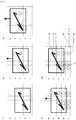
- an xy coordinate system is conceptually placed on the screen of a surface sensor, there are different courses for the actual movement of the device and the signals detected by the surface sensor, the deviations being in particular due to the presence of the electrically conductive structure.
- the inventors have recognized that when performing a Relative movement between a device which has a suitable electrically conductive structure and a surface sensor generates a periodic signal which manifests itself in the conceptually xy coordinate system described above, in particular as a wiggle, loop or zigzag pattern.
- the signal detected by the area sensor "oscillates" around a fixed central position, the deviations downward or upward being referred to as "amplitudes".
- the terms “oscillate”, “oscillate” or “wiggle” are used synonymously with one another.
- the theoretical coordinate system can be placed on the screen of the area sensor in such a way that the x-axis of the coordinate system coincides with the fixed central position around which the periodic signal fluctuates.
- the course of the periodic signal can then advantageously be represented as a function y (x), it being preferred in the sense of the invention that this function y (x) has a periodicity.
- the terms “repeating”, “repeating”, “repeating at intervals", "cyclically” or “repetitive” are used synonymously for the term "periodic” and among themselves.
- the periodicity described here in connection with the mental coordinate system is preferably referred to in the sense of the invention as spatial periodicity.
- the periodic signal has a periodicity in terms of time.
- the x and / or the y coordinate of the periodically running signal can each be represented as a function of time, that is to say as a function of the x coordinate x (t) and as a function of the y coordinate of the periodic signal y ( t).
- the periodic signal represents a temporally periodic change in size, while in the case described above it represents a spatially periodic change in size, in which preferably spatially varying sizes are described.
- the periodic signal that is generated in the context of the present invention is also time-dependent.
- the temporal periodicity is preferably characterized by the period of the signal.
- a dynamic signal which in the sense of the present invention is intended to mean in particular that the periodic signal changes while the device is being moved over the area sensor, ie during the relative movement between the electrically conductive structure and the area sensor.
- the electrically conductive structure acts as a signal transmitter or functions as such.
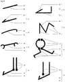
- the electrically conductive structure can additionally be characterized by the design of at least one partial element.
- the term design includes, but is not limited to, shape, size, geometry, length, width, orientation, position and angle of the element of the electrically conductive structure.
- Preferred design variants include, for example, linear main and / or partial elements, which are characterized by length, width and angle. It is preferred that the sub-elements are galvanically connected to the main element and in their entirety form the electrically conductive structure. It is particularly preferred that the electrically conductive structure is open, ie has open ends or in other words is characterized by a start and an end and / or is not connected to a ring or a similar self-contained figure or geometry.
- the course of the periodic signal is influenced or fixed in particular by the centroid of the area of the electrically conductive structure or by partial areas of the electrically conductive structure. It is particularly preferred that the area center of gravity of partial areas interacts with the electrode grid of the capacitive area sensor. In other words, it can be particularly preferred that the centroid overlaps with selected electrode crossings and thus interacts at this point.
- the area center of gravity of the electrically conductive structure can be formed, for example, by the geometric center of gravity of the area covered by the electrically conductive structure. It can also be preferred that each partial element forms a center of gravity together with the main element.
- the center of gravity of the electrically conductive structure is influenced by the mass distribution and / or area coverage of the electrically conductive material that forms the electrically conductive structure, so that a weighted centroid of the area of the electrically conductive structure can be determined.
- a period length can be assigned to the periodic signal as a characterizing variable of the periodic signal, the period length preferably corresponding to the reciprocal of the spatial frequency with which the periodic signal fluctuates.
- the period length is determined by the arrangement and / or design of the electrode grid of the area sensor. It was particularly surprising that the spatial frequency of the periodic signal correlated with the lattice constant of the electrode lattice of the area sensor. In other words, in the sense of the invention it is preferred that the spatial or local periodicity of the periodic signal is determined by the arrangement and / or the design of the electrode grid of the area sensor.
- the period length of the periodic signal is determined by the geometry of the electrode grid in the capacitive surface sensor, the arrangement and / or design of the electrode grid of the surface sensor preferably also being referred to as the "geometry of the electrode grid".
- the period length of the signal reflects the arrangement of the electrodes in the electrode grid of the area sensor.
- the period length of the signal is between 2 and 9 mm.
- the period length of the signal correlates with the geometry of the electrode grid, in particular with the grid constant.
- the lattice constant in capacitive area sensors is preferably in the range between 2 and 9 mm.
- the period length is preferably at least 3 mm and a maximum of 7 mm, since this area surprisingly correlates with the lattice constant of capacitive area sensors, in particular from mobile telephones, smartphones, tablets or comparable devices. It is particularly preferred that the period length of the signal is between 4 and 5 mm.
- a corresponding lattice constant in capacitive area sensors is particularly suitable for reliably detecting finger inputs on capacitive area sensors.
- the periodic signal can also be assigned a period as a characterizing variable of the periodic signal, the period duration preferably corresponding to the reciprocal of the frequency with which the periodic signal fluctuates.
- the period ie the temporal periodicity of the periodic signal, is determined by the geometry of the electrode grid of the surface sensor in conjunction with the speed of the relative movement with which the device is moved via the surface sensor.
- the x and / or the y coordinate of the periodically running signal can each be represented as a function of time, that is to say as a function of the x coordinate x (t) and as a function of the y coordinate of the periodic signal y ( t).
- the periodic signal has a period of at least 25 ms and particularly preferably of at least 50 ms. It is furthermore particularly preferred that the periodic signal has a period of at most 1 s and particularly preferably of at most 500 ms.
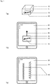
- the device or the three-dimensional object is formed by a packaging or a folding box. It is further preferred that the three-dimensional object is abbreviated as "object”.
- the object is preferably a cuboid structure that has a height, a width and a length.
- the object has six side faces.
- the side surface of the object which faces the surface sensor is preferably referred to as the underside of the object.
- the surface of the object that faces the surface sensor is alternatively also referred to as the contact surface and does not necessarily have to be the underside of the object in relation to the intended use of the object.
- the underside and the contact surface are used synonymously and refer here to the function of this surface, to be suitable for interacting with the capacitive surface sensor.
- the side surface of the object that lies opposite the underside is preferably referred to as the top of the object.
- the remaining four surfaces of the object are preferably referred to as side surfaces.
- the wording that the electrically conductive structure is arranged at least on the underside of the three-dimensional object means in the sense of the invention that the electrically conductive structure is in any case on the underside of the object and in a preferred embodiment of the invention only there. In other words, the entire electrically conductive structure is present in this preferred embodiment of the invention on the underside or contact surface of the device. In the sense of the invention, it is particularly preferred that the entire electrically conductive structure is suitable for interacting with the electrode grid of the capacitive area sensor.
- the electrically conductive structure is essentially completely arranged on the underside of the object.
- the electrically conductive structure is arranged on the inside of the underside of the three-dimensional object, for example a folding box.
- the electrically conductive structure can be provided by a color layer and / or a lacquer layer and / or optically covered by a laminate material so that the electrically conductive structure is not visible to the user.
- the interaction between the electrically conductive structure and the capacitive area sensor is preferably a capacitive interaction, ie there is no direct galvanic contact between the electrically conductive structure and the area sensor.
- the shape of the object is not limited to cuboid or cube-shaped geometries. Other shapes, for example cylinders, tetrahedra or other shapes or bodies, are also possible embodiments.
- individual elements or subregions of the electrically conductive structure also, i.e. additionally also exist on one side surface or several side surfaces of the object.
- at least a part of the electrically conductive structure is suitable for interacting with the electrode grid of the capacitive area sensor.
- a contact surface can be arranged on one of the side surfaces of the device or the three-dimensional object.
- a contact surface is a sub-element of the electrically conductive structure, which is designed such that it is conductively connected to the electrically conductive structure, so that by touching the contact surface of the electrically conductive structure, a potential change in the system comprising the electrically conductive structure and the area sensor is caused, this potential change can preferably be detected by the area sensor.
- touch surface is used synonymously for touch surface.
- the width and length of the object is significantly larger than the height of the object.
- Such an object can be described, for example, as a card-shaped object and is characterized in that it represents an essentially flat object. It may further be preferred that the flat object is flexible and / or bendable.
- the side surface of the object that faces the surface sensor is preferably referred to as the underside of the object, while the side surface of the object that lies opposite the underside is referred to as the top of the object.
- the remaining four side surfaces are preferably referred to as side surfaces.
- the electrically conductive structure is arranged at least on the underside of the three-dimensional object preferably means in the sense of the invention that the electrically conductive structure is in any case the underside of the object is present and in a preferred embodiment of the invention only there. In other words, the entire electrically conductive structure is present on the underside of the device in this preferred embodiment of the invention. In the sense of the invention, it is particularly preferred that the entire electrically conductive structure is suitable for interacting with the electrode grid of the capacitive area sensor. This is preferably achieved in that the electrically conductive structure is essentially completely arranged on the underside of the object.
- Surface sensors include in particular at least one active circuit, which is preferably referred to as a touch controller, which can be connected to a structure of electrodes.
- this electrode structure is preferably also referred to as an “electrode grid”.
- Surface sensors are known in the prior art, the electrodes of which comprise groups of electrodes which differ from one another in their function, for example. These can be, for example, transmitting and receiving electrodes, which can be arranged in a particularly preferred arrangement in column and row form, that is to say in particular form nodes or intersections at which at least one transmitting and one receiving electrode cross each other or overlap.
- the intersecting transmitting and receiving electrodes are preferably aligned with one another in the region of the nodes such that they essentially enclose a 90 ° angle with one another.
- an electrostatic field is formed between the transmitting and receiving electrodes of the area sensor, which field is sensitive to changes. These changes can be caused, for example, by touching the surface of the surface sensor with a finger or a conductive object, by touching a touching or touching surface of an electrically conductive structure that is at least partially on the surface sensor, or in particular by bringing the surface sensor into contact with an electrically conductive structure, which is arranged, for example, on the underside of a device.
- Such changes lead to potential changes within the electrostatic field, which is preferably caused by the fact that, for example, touching a contact surface of an electrically conductive structure locally reduces the electrical field between the transmitting and receiving electrodes.
- Such a change in the potential relationships is detected and processed by the electronics of the touch controller.
- the touch controller preferably controls the electrodes in such a way that a signal is transmitted between one or more transmitting electrodes and one or more receiving electrodes, which is preferably an electrical signal, for example a voltage, a current or a potential (difference) can act.
- a signal is transmitted between one or more transmitting electrodes and one or more receiving electrodes, which is preferably an electrical signal, for example a voltage, a current or a potential (difference) can act.
- These electrical signals in a capacitive area sensor are preferably evaluated by the touch controller and processed for the operating system of the device.
- the information transmitted from the touch controller to the operating system describes so-called individual “touches” or “touch events”, which can be thought of as individual detected touches or as individual inputs.
- These touches are preferably characterized by the parameters "x coordinate of the touch", "y coordinate of the touch”, "time stamp of the touch” and "type of touch”.
- the "x and y coordinate” parameters describe the position of the input on the touchscreen. Each pair of coordinates is preferably assigned a time stamp that describes when the entry was made at the corresponding point.
- the "Type of touch event” parameter describes the detected status of the input on the touchscreen.
- the specialist is, among others, the types Touch Start, Touch Move, Touch End and Touch Cancel are known. With the help of the parameters Touch Start, at least one Touch Move and Touch End as well as the associated coordinates and time stamps, a touch input on the capacitive area sensor can be described. It is preferred and known in the prior art as multitouch technology that several touch inputs can be evaluated simultaneously.
- the periodic signal preferably comprises a number of such touches or touch inputs, the properties of the signal preferably depending on the specific shape of the electrically conductive structure and on the structural arrangement of the transmit and receive electrodes of the area sensor.
- the periodic signal is formed by a set of touches and / or touch inputs which have recurring properties and / or a periodicity in spatial and / or temporal terms.
- the course of the periodic signal is determined by the electrically conductive structure.
- the term “capacitive area sensor” preferably refers to devices that have touch sensors and are able to perceive external influences or influences, for example contacts, on the surface of the touch sensor and to evaluate them by means of integrated logic. Such Area sensors are used, for example, to make machines easier to use.
- touch sensors which are primarily used for input
- touchscreens that are also display and / or output devices.
- special input pens or similar devices can be used in addition to the fingers.
- fingers and special input pens are preferably combined under the term input means. These are preferably able to change an electrostatic field between row and column electrodes within the area sensor.
- the capacitive, preferably touch-sensitive screen is preferably set up to detect the position of the finger or stylus.
- the invention represents a significant deviation from the known prior art, since experts have previously assumed that activation of an electrically conductive structure, for example by touching a user, is necessary in order to be recognized by the capacitive area sensor.
- the present invention now discloses a device and a system in which an input means for generating a periodic signal can surprisingly be dispensed with.
- the area sensor is able to recognize the electrically conductive structure of the device without the structure being activated by user contact is advantageously based on a coupling between the capacitive area sensor and the electrically conductive structure, which exists in particular if the electrically conductive structure with at least two rows and at least two columns, or at least two transmitting electrodes and at least two receiving electrodes, of the electrode grid of the capacitive area sensor interacts.
- the electrically conductive structure overlaps with at least two electrode crossings. A charge carrier exchange can then occur between the surface sensor, or its electrodes, and the electrically conductive structure.
- the electrically conductive structure on the three-dimensional object causes the electrodes of the electrode grid in the area sensor to interact indirectly with one another via the electrically conductive structure. It is very particularly preferred in the sense of the invention that the electrically conductive structure is set up to bridge a distance between the at least two transmitting and receiving electrodes. In this way, a capacitive connection between at least two different electrode crossings is preferably created, which is produced and held in particular by the electrically conductive structure. In the sense of the invention, it is preferred that the electrically conductive structure connects the columns and rows of the electrode grid of the area sensor to one another, so that an interaction between the at least four affected electrodes (two transmitting electrodes and two receiving electrodes) is brought about here.
- the electrically conductive structure is set up to effect bridging and / or connections of electrode crossings within the electrode grid of the area sensor.
- the connection and / or bridging of the electrode crossings is preferably based on a capacitive interaction, which is also referred to as capacitive coupling.
- the connection and / or bridging is not based on a galvanic connection, but on a capacitive connection. This can advantageously lead to self-induced signal generation, in particular to generation of the desired periodic signal when the device is moved via the capacitive area sensor.
- the electrically conductive structure comprises at least one main element. In a further preferred embodiment, the electrically conductive structure comprises at least one partial element in addition to the main element.
- the main element and one or more sub-elements are galvanically connected to one another and form the electrically conductive structure as a whole.
- the electrically conductive structure can be characterized by the design of the main element and the design of the sub-elements.
- the term design includes, but is not limited to, shape, size, geometry, length, width, orientation, position and angle of the element of the electrically conductive structure.
- Main and / or sub-elements can, for example, be linear, circular or arc-shaped without being limited to this.
- the transition between the sub-element and the main element can also be fluid or curved. It can also be preferred to connect a partial element to a further partial element galvanically instead of the partial element.
- the number, arrangement and orientation of the sub-elements is not limited to the variants described.
- the entirety of the main and partial elements that are galvanically connected to one another is referred to as an electrically conductive structure. It can also be preferred that two or more electrically conductive structures are located on a contact surface of the object, which are characterized in that they are not galvanically connected to one another.
- the electrically conductive structure interacts with the electrode grid of the capacitive area sensor.
- various electrode crossings interact with the electrically conductive structure or one or more centroids of the area of the electrically conductive structure.
- An electrode crossing interacts with the electrically conductive structure in particular when the electrically conductive structure overlaps selected electrode crossings at a time x.
- the centroids of the electrically conductive structure interact with the capacitive area sensor or the electrode grid.
- the capacitive area sensor is activated or, in other words, a touch event is generated.
- the electrically conductive structure or the centroids gradually interact with other electrode crossings. This results in a superimposition of two different geometries: on the one hand the geometry of the electrode grid and on the other hand the geometry of the electrically conductive structure. If these two geometries are shifted against each other, the two geometries overlap. This superposition is repeated cyclically or periodically. This leads to periodically arranged touch events on the capacitive area sensor, which in their entirety form the periodic signal.
- the electrically conductive structure interacts with at least two rows and at least two columns at any time during the movement. It is particularly preferred that the two columns and / or two rows are not adjacent. In other words, it is preferred that the electrically conductive structure connects two bridged rows and / or two spaced columns with one another or bridges them.
- this connection between different electrode crossings or the transmitting and receiving electrodes of the electrode grid makes the activation of the electrically conductive structure by touching a user obsolete, so that surprisingly in the context of the present invention the use of a Input means, such as a user's finger, can be omitted.
- the advantageous effects and technical effects of the invention are preferably based on the interaction between the electrically conductive structure and the area sensor, particularly preferably between the electrically conductive structure and the electrode grid of the area sensor and most preferably between the electrically conductive structure and the columns and rows or the Transmitting and receiving electrodes of the electrode grid of the area sensor.
- this interaction preferably leads to a change in the electrostatic field between the electrodes in a surface sensor and / or to a measurable change in the capacitance.
- the change in the electrostatic field can be brought about in particular by a relative movement between the surface sensor and the three-dimensional object.
- the periodic signal is generated by a relative movement between the electrically conductive structure and the area sensor.
- this relative movement can preferably also be referred to as a dynamic operative contact.
- the duration of the relative movement determines the duration of the periodic signal. Duration in this context means in particular the total duration of the signal.
- the periodic signal has a duration of at least 250 ms, preferably of at least 500 ms and particularly preferably of at least 750 ms.
- the present invention also turns away from the prior art in that a touch structure on the device is no longer required to generate a signal on the surface sensor.
- a touch structure presupposes a certain spatial structure of predefined elements of an electrically conductive structure, namely in particular a touch point, a coupling surface and line means for connection.
- the presence of these predefined elements and their functionalities is not necessary in the context of the present invention, as is the need to emulate or imitate the properties of fingertips with the electrically conductive structure.
- the proposed device does not require a special coupling surface that must be touched by a user in order to activate the electrically conductive structure for the surface sensor.
- Area sensors are usually provided in an electrical device, which may be smartphones, cell phones, displays, tablet PCs, tablet notebooks, touchpad devices, graphics tablets, televisions, PDAs, MP3 players, trackpads and / or capacitive input devices, without being limited to it.
- Touchscreens are preferably also referred to as touch screens, area sensors or sensor screens.
- a surface sensor does not necessarily have to be used in connection with a display or a touchscreen. It can also be preferred in the sense of the invention that the surface sensor is visible or invisible integrated in devices, objects and / or devices. For the purposes of the invention, it can be preferred, for example, to use multitouch-capable surface sensors. Such surface sensors are preferably set up to detect multiple touches at the same time, which means that, for example, elements that are displayed on a touchscreen can be rotated or scaled using special gestures.
- the electrically conductive structure is set up to determine a course of the periodic signal with regard to a curve course, an amplitude and / or a flank course.
- the design of the electrically conductive structure defines the course of the periodic signal, in particular the course of the curve, the amplitudes and / or the slope.
- the term “curve profile” preferably describes the graphical representation or reproduction of the y (x) function in the coordinate system, which can be placed on the screen of the area sensor.
- the term describes the course of the y (x) function in the virtual coordinate system.
- amplitude describes prefers the maximum deviation from a fixed central position around which the periodic signal can fluctuate. It is preferred in the sense of the invention that the amplitude of the signal is at least 1 mm, so that the amplitude of the periodic signal can be evaluated when evaluating the amount of touch signals or touch events.
- the amplitude is preferably at least 2 mm and particularly preferably at least 3 mm. It was particularly surprising that possible deviations or tolerances, which can be caused by the relative movement between the device and the capacitive area sensor, can be neglected in the analysis of the signal and the signal-to-noise ratio is as large as possible, ie the amplitude of the periodic signal is as large as possible compared to possible deviations.
- the amplitude of the periodic signal is a maximum of 60 mm, since this corresponds to the approximate maximum width of today's capacitive area sensors in mobile telephones or smartphones.
- the amplitude of the periodic signal is particularly preferably a maximum of 40 mm, since a corresponding periodic signal can be evaluated particularly well.
- a corresponding signal can be evaluated particularly well in combination with a further periodic signal.
- edge profile preferably describes the profile of the signal in more detail and includes, but is not limited to, the variables rise, fall and edge steepness.
- the electrically conductive structure is set up to define a periodic non-harmonic signal.
- Non-harmonic signals can preferably be represented from an overlap of several harmonic signals.
- the appearance of the signal can also be described as fidgeting, wobbling or trembling.
- the location-dependent signal has a loop-shaped course.
- the electrically conductive structure is set up so that the coordinate of the signal, in the direction of which the device is moved via the capacitive area sensor, periodically increases and decreases, i.e. the signal runs partially backwards relative to the direction of movement of the electrically conductive structure.
- the course on the capacitive area sensor can be represented as a loop or I-shaped course (small script L) of the signal.
- the electrically conductive structure both on the contact surface, ie on the surface of the device, for the active contact with the surface sensor is provided, and is also present on at least one further surface of the device.
- the electrically conductive structure is present both on the underside, which serves as a contact surface, and on at least one side surface of the device. This feature is essentially synonymous with the statement that at least part of the electrically conductive structure is suitable for interacting with the electrode grid of the capacitive surface sensor.
- the part of the electrically conductive structure that interacts with the surface sensor is preferably the part of the electrically conductive structure that is arranged on the contact surface of the three-dimensional object.
- At least a part of the electrically conductive structure is present on the contact surface of the three-dimensional object, while in preferred embodiments of the invention it can also be preferred that in addition to the parts of the electrically conductive structure that are present on the contact surface of the device, further parts of the electrically conductive structure Structure on the adjacent surfaces of the device. It can therefore be preferred in the sense of the invention that essentially the entire electrically conductive structure is present on the contact surface of the three-dimensional object or only a portion of the electrically conductive structure.
- the corresponding device is particularly simple to manufacture, since only one side of the three-dimensional object has to be printed or provided with electrically conductive material.
- This feature is essentially synonymous with the statement that the entire electrically conductive structure is suitable for interacting with the electrode grid of the capacitive area sensor.
- this embodiment of the invention avoids difficulties which may arise, for example, if an element of the electrically conductive structure is present on two sides of the object, in the sense that this element must then run over an edge of the object.
- a disadvantage in the prior art is the need for the electrically conductive structure to be guided over one or more edges of a three-dimensional object.
- edges of the object are exposed to greater mechanical loads than, for example, the inner surfaces of the side surfaces or the underside of the object.
- the manufacturing process of a folding box particularly in the processes of creasing, punching, erecting, gluing and assembling, there are strong mechanical loads, particularly in the area of the edges of the folding box.
- This can lead to a reduction in the electrical conductivity or even breakage of the electrically conductive structure.
- the arrangement of the electrically conductive structure only on one side of the object represents a decisive advantage over the solutions known from the prior art.
- the electrically conductive structure is set up to interact with at least two rows and at least two columns of an electrode grid of the capacitive area sensor. It is preferred in the sense of the invention that the rows of the electrode grid of the area sensor are essentially formed by transmitting electrodes and the columns of the electrode grid of the area sensor are essentially formed by receiving electrodes, or vice versa. In the sense of the invention, it is particularly preferred that the columns of the electrode grid of the area sensor comprise either only transmitting electrodes or only receiving electrodes. It is further preferred that the rows of the electrode grid of the area sensor are also formed by type, either only from transmitting electrodes or only from receiving electrodes.
- the electrically conductive structure of the three-dimensional object is set up to interact with at least two receiving electrodes and at least two transmitting electrodes of the electrode grid of the capacitive area sensor. It can be preferred that there are two adjacent transmission and reception electrodes. In a further embodiment, it can in particular also be preferred that the transmitting and / or receiving electrodes are spaced apart, that is to say that there are further electrodes between the electrodes which interact.
- the transmitter electrodes, which are preferably arranged next to one another, are preferably arranged essentially parallel to one another. It is also preferred that the reception electrodes, which are preferably arranged next to one another, are arranged essentially parallel to one another.
- the receiving electrodes of the electrode grid of the area sensor are arranged essentially perpendicular to the transmitting electrodes of the electrode grid, the term “essentially” being not unclear to the average person skilled in the art, because the average person skilled in the art knows how the term is to be understood in practice.
- the person skilled in the art also knows, in particular, that slight deviations from exact parallelism or orthogonality can arise, for example, due to the manufacturing process. However, within the meaning of the invention, such deviations should also be encompassed by the formulations “essentially parallel” and “essentially perpendicular”.
- a pattern similar to a check pattern preferably results between two transmitting and receiving electrodes, which are preferably located next to one another. It is very particularly preferred in the sense of the invention that the electrically conductive structure interacts with at least two rows and at least two columns, or at least two transmitting electrodes and at least two receiving electrodes, of the electrode grid of the capacitive area sensor. It has surprisingly been found that the course of the periodic signal is determined by the interaction of partial areas of the electrically conductive structure with the electrode grid of the capacitive area sensor, this determination of the periodic signal in particular by the interaction between the specific design of the electrically conductive structure with the at least two transmitting and receiving electrodes is reached.
- the invention relates to a system for generating a periodic signal on a capacitive area sensor, the system comprising a device, and a capacitive area sensor.
- the system is characterized in that the periodic signal on the capacitive area sensor is generated by a relative movement between the electrically conductive structure and the area sensor.
- the electrically conductive structure on the device is set up to interact with the electrode grid of the capacitive area sensor to determine the course of the periodic signal.
- a system for generating a periodic signal on a capacitive area sensor can be provided in such a way that the provision or use of a special input means can be dispensed with.
- the invention surprisingly manages without human coupling.
- the proposed system comprises a device, which is preferably a three-dimensional object, and a capacitive area sensor, which in the sense of the invention is preferably abbreviated as "area sensor".
- area sensor preferably abbreviated as "area sensor”.
- the course of the periodic signal is determined in particular by the configuration of the electrically conductive structure on the device, while the period length of the periodic signal is determined by the configuration of the area sensor, in particular its electrode grid composed of transmit and receive electrodes.
- the period length of the periodic signal is determined by the geometry of the electrode grid in the capacitive area sensor.
- the arrangement and / or design of the electrode grid of the surface sensor can preferably also be referred to as “geometry of the electrode grid”.
- the duration of the interaction between the electrically conductive structure and the area sensor determines the duration of the periodic signal.
- the duration of the periodic signal in this context means in particular the total duration of the periodic signal. It is particularly preferred in the sense of the invention that the periodic signal has a duration of at least 250 ms, since a minimum duration of the periodic signal is required so that the characteristic values of the signal can be evaluated accordingly.
- the duration of the periodic signal is particularly preferably at least 500 ms, since a larger number of touch data or touch events are available for evaluation and mean values can be formed from the key figures, for example the amplitude of the signal.
- the periodic signal has a particularly preferred minimum duration of at least 750 ms.
- the proposed system thus makes it possible to generate a periodic signal on a surface sensor by moving a device, in particular a three-dimensional object, over the surface sensor.
- a device in particular a three-dimensional object
- the deliberate and intentional generation of periodic signals by a specific configuration or design of an electrically conductive structure on a device or by a specific configuration or geometry of the electrode grid of a surface sensor has not previously been described in the prior art. It was completely surprising that the properties of the periodic signal to be generated can be deliberately influenced, varied and / or changed by the specific configuration or influence and / or change in the structural configuration of the electrically conductive structure and / or the electrode grid.
- the properties of the periodic signal that can be set in this way are preferably the spatial and / or temporal properties of the periodic signal, for example its amplitude or period length or period duration. It was completely surprising that the spatial and / or temporal properties of a periodic signal can be influenced by the provision of a system comprising a device with an electrically conductive structure and an area sensor. It was completely surprising that the invention made it particularly intuitive and user-friendly Interactive system can be provided, with the help of which an object or its user can be verified and / or identified particularly reliably and uniquely by a capacitive area sensor. The proposed device and the proposed system are particularly secure against manipulation and the corresponding electrically conductive structure in particular cannot be copied by fingertips or manipulated by a user.
- the term “identification” preferably means that a device or an object is recognized by the area sensor and can be assigned, for example, to a data record stored in the electrical device that contains the area sensor.
- the data record may also not be stored directly in the electrical device, but may be accessible to it by being available, for example, on a server, on the Internet and / or in a cloud.
- the detection of the object by the area sensor takes place in particular by the detection of the electrically conductive structure which is arranged on the object. This electrically conductive structure is determined in particular by the design of the entire electrically conductive structure and / or its partial areas.
- the term “verification” preferably means that the authenticity or the authenticity of an object can be ascertained or proven.
- holograms have long been known in the prior art. However, it is often only possible for experts to check or prove the authenticity of a hologram. It was completely surprising that the present invention enables the feature in the form of the electrically conductive structure to be verified beyond any doubt with the aid of a device which includes a surface sensor, for example a smartphone. Areas of application for such an application are in the area of product and document protection.
- the electrically conductive structure on an object serves as an access key to digital content.
- the electrically conductive feature be used as a key for the activation of digital content, for example guarantee certificates, vouchers, coupons, digital media, etc. serves.
- the periodic signal on the capacitive area sensor is generated by a relative movement between the electrically conductive structure and the area sensor.
- the device or the object is preferably for generating such a periodic signal on a Capacitive area sensor set up, wherein the periodic signal is generated in particular by a relative movement between the electrically conductive structure and the area sensor.
- this preferably means that the device and the area sensor are displaced relative to one another, so that a movement of the two objects relative to one another is brought about. This can be done, for example, by moving the object on the screen of an area sensor or moving it over it.
- the device or its contact surface preferably lies on the screen of the surface sensor. It is very particularly preferred in the sense of the invention that the device is pulled over the area sensor in order to obtain a relative movement with which the periodic signal is generated on the area sensor. This pulling or pushing movement is preferably referred to as a relative movement.
- the duration of the relative movement determines the duration of the periodic signal. Duration in this context means in particular the total duration of the signal. It is particularly preferred in the sense of the invention that the periodic signal has a duration of at least 250 ms, preferably of at least 500 ms and particularly preferably of at least 750 ms.
- the invention relates to the use of the proposed device for generating a periodic signal on a capacitive area sensor, the electrically conductive structure of the device being brought into active contact with the capacitive area sensor and the device being moved relative to the capacitive area sensor.
- the electrically conductive structure is applied to a substrate material by means of film transfer processes, for example cold film transfer, hot stamping and / or thermal transfer, without being restricted to these application processes.
- film transfer processes for example cold film transfer, hot stamping and / or thermal transfer
- printing processes such as, for example, offset printing, gravure printing, flexographic printing, screen printing and / or inkjet methods, can be used to produce the electrically conductive structure on the non-conductive substrate, without being limited thereto.
- Suitable electrically conductive paints include materials that are based, for example, on metal particles, nanoparticles, carbon, graphene and / or electrically conductive polymers, without being limited to these materials.
- the electrically conductive structure can also be preferred to cover the electrically conductive structure with at least one further layer, this layer being a paper or film-based laminate material or at least one lacquer / color layer.
- This layer can be optically transparent or opaque his.
- the electrically conductive structure is applied on the inside of a side surface of the object, for example on the inside of the contact surface or underside of a folding box.
- a feature of classic conventional printing processes is the simple and quick duplication of a motif, in that the motif to be printed is applied to a printing form, for example a gravure cylinder or an offset printing plate, and can then be reproduced several times and at high speed.
- Conventional printing processes are not suitable for producing individualized content, since the printing form production represents a significant part of the total production costs. This means that only larger print runs can be produced economically.
- graphic printing digital printing processes exist for the production of short runs and individualized products, with which individual contents can be printed economically. These printing processes include, for example, electrophotography, laser printing or inkjet printing. It is also possible to produce individualized electrically conductive structures by means of process combinations of conventional printing processes and additive or subtractive processes.
Landscapes
- Engineering & Computer Science (AREA)
- General Engineering & Computer Science (AREA)
- Theoretical Computer Science (AREA)
- Human Computer Interaction (AREA)
- Physics & Mathematics (AREA)
- General Physics & Mathematics (AREA)
- Position Input By Displaying (AREA)
Priority Applications (5)
| Application Number | Priority Date | Filing Date | Title |
|---|---|---|---|
| KR1020217011207A KR20210057165A (ko) | 2018-09-17 | 2019-09-17 | 용량성 표면 센서에서 주기적 신호를 생성하기 위한 디바이스, 사용 및 시스템 |
| US17/276,259 US20220035505A1 (en) | 2018-09-17 | 2019-09-17 | Device, its use and system for generating a periodic signal on a capacitive surface sensor |
| CN201980060682.6A CN112703465A (zh) | 2018-09-17 | 2019-09-17 | 在电容表面传感器上产生周期性信号的装置、用途及系统 |
| EP19773757.0A EP3853701B1 (fr) | 2018-09-17 | 2019-09-17 | Dispositif, son utilisation et système de génération d'un signal périodique sur un capteur superficiel capacitif |
| PCT/EP2019/074783 WO2020058231A1 (fr) | 2018-09-17 | 2019-09-17 | Dispositif, son utilisation et système pour générer un signal périodique sur un capteur surfacique capacitif |
Applications Claiming Priority (1)
| Application Number | Priority Date | Filing Date | Title |
|---|---|---|---|
| EP18000747 | 2018-09-17 |
Publications (1)
| Publication Number | Publication Date |
|---|---|
| EP3623914A1 true EP3623914A1 (fr) | 2020-03-18 |
Family
ID=63787650
Family Applications (2)
| Application Number | Title | Priority Date | Filing Date |
|---|---|---|---|
| EP19164305.5A Withdrawn EP3623914A1 (fr) | 2018-09-17 | 2019-03-21 | Dispositif, son utilisation et système de génération d'un signal périodique sur un capteur superficiel capacitif |
| EP19773757.0A Active EP3853701B1 (fr) | 2018-09-17 | 2019-09-17 | Dispositif, son utilisation et système de génération d'un signal périodique sur un capteur superficiel capacitif |
Family Applications After (1)
| Application Number | Title | Priority Date | Filing Date |
|---|---|---|---|
| EP19773757.0A Active EP3853701B1 (fr) | 2018-09-17 | 2019-09-17 | Dispositif, son utilisation et système de génération d'un signal périodique sur un capteur superficiel capacitif |
Country Status (5)
| Country | Link |
|---|---|
| US (1) | US20220035505A1 (fr) |
| EP (2) | EP3623914A1 (fr) |
| KR (1) | KR20210057165A (fr) |
| CN (1) | CN112703465A (fr) |
| WO (1) | WO2020058231A1 (fr) |
Families Citing this family (1)
| Publication number | Priority date | Publication date | Assignee | Title |
|---|---|---|---|---|
| DE102021003493A1 (de) | 2021-07-06 | 2023-01-12 | Giesecke+Devrient Currency Technology Gmbh | Sicherheitsdokument und Verfahren zur Herstellung eines Sicherheitsdokuments |
Citations (5)
| Publication number | Priority date | Publication date | Assignee | Title |
|---|---|---|---|---|
| WO2011154524A1 (fr) | 2010-06-11 | 2011-12-15 | Printechnologics Gmbh | Système doté d'un support d'informations capacitif servant à détecter des informations |
| WO2012072648A1 (fr) | 2010-11-29 | 2012-06-07 | Printechnologics Gmbh | Système et procédé de récupération d'informations à partir d'un support d'informations au moyen d'un écran tactile capacitif |
| WO2016131963A1 (fr) | 2015-02-19 | 2016-08-25 | T+Ink Gmbh | Support d'informations capacitif de mise à la terre autonome et son utilisation |
| WO2018141479A1 (fr) | 2017-01-31 | 2018-08-09 | Prismade Labs Gmbh | Dispositif et son utilisation pour générer un signal fonction du temps sur un capteur surfacique capacitif, ainsi qu'une structure électroconductrice destinée à un tel dispositif |
| WO2018141478A1 (fr) | 2017-01-31 | 2018-08-09 | Prismade Labs Gmbh | Procédé de génération d'un signal dépendant du temps sur un capteur surfacique capacitif, procédé d'identification d'un objet de type carte, objet de type carte et son utilisation |
Family Cites Families (2)
| Publication number | Priority date | Publication date | Assignee | Title |
|---|---|---|---|---|
| US7762470B2 (en) * | 2003-11-17 | 2010-07-27 | Dpd Patent Trust Ltd. | RFID token with multiple interface controller |
| US8803814B2 (en) * | 2009-03-13 | 2014-08-12 | Adobe Systems Incorporated | Surface scanning with a capacitive touch screen |
-
2019
- 2019-03-21 EP EP19164305.5A patent/EP3623914A1/fr not_active Withdrawn
- 2019-09-17 US US17/276,259 patent/US20220035505A1/en not_active Abandoned
- 2019-09-17 KR KR1020217011207A patent/KR20210057165A/ko unknown
- 2019-09-17 EP EP19773757.0A patent/EP3853701B1/fr active Active
- 2019-09-17 CN CN201980060682.6A patent/CN112703465A/zh active Pending
- 2019-09-17 WO PCT/EP2019/074783 patent/WO2020058231A1/fr unknown
Patent Citations (5)
| Publication number | Priority date | Publication date | Assignee | Title |
|---|---|---|---|---|
| WO2011154524A1 (fr) | 2010-06-11 | 2011-12-15 | Printechnologics Gmbh | Système doté d'un support d'informations capacitif servant à détecter des informations |
| WO2012072648A1 (fr) | 2010-11-29 | 2012-06-07 | Printechnologics Gmbh | Système et procédé de récupération d'informations à partir d'un support d'informations au moyen d'un écran tactile capacitif |
| WO2016131963A1 (fr) | 2015-02-19 | 2016-08-25 | T+Ink Gmbh | Support d'informations capacitif de mise à la terre autonome et son utilisation |
| WO2018141479A1 (fr) | 2017-01-31 | 2018-08-09 | Prismade Labs Gmbh | Dispositif et son utilisation pour générer un signal fonction du temps sur un capteur surfacique capacitif, ainsi qu'une structure électroconductrice destinée à un tel dispositif |
| WO2018141478A1 (fr) | 2017-01-31 | 2018-08-09 | Prismade Labs Gmbh | Procédé de génération d'un signal dépendant du temps sur un capteur surfacique capacitif, procédé d'identification d'un objet de type carte, objet de type carte et son utilisation |
Also Published As
| Publication number | Publication date |
|---|---|
| EP3853701A1 (fr) | 2021-07-28 |
| CN112703465A (zh) | 2021-04-23 |
| US20220035505A1 (en) | 2022-02-03 |
| EP3853701B1 (fr) | 2023-12-06 |
| WO2020058231A1 (fr) | 2020-03-26 |
| KR20210057165A (ko) | 2021-05-20 |
Similar Documents
| Publication | Publication Date | Title |
|---|---|---|
| DE102015108278B4 (de) | Integriertes elektromagnetisches und kapazitives berührungssubstrat, berührungsfeld und berührungs-anzeigefeld | |
| EP3577601B1 (fr) | Procédé de production d'un signal dépendant du temps sur un capteur de zone capacitif et procédé d'identification d'un objet de carte, et objet de carte et utilisation de celui-ci | |
| DE102009017419B4 (de) | Kapazitiver Positionssensor | |
| DE102014210267A1 (de) | Kapazitive Mehrzustandstaste | |
| DE102010027732A1 (de) | Zweidimensionaler Positionssensor | |
| DE102014215662A1 (de) | Elektronisches Gerät und Koordinatenerfassungsverfahren | |
| DE202012101382U1 (de) | Flexibler Berührungssensor | |
| DE202012101478U1 (de) | Berührungssensor mit Gegenkapazitätselektroden und Eigenkapazitätselektroden | |
| DE202012102572U1 (de) | Differentielle Detektion in einem aktiven Stift | |
| DE202012103379U1 (de) | Berührungssensor mit Stromspiegel zur Eigenkapazitätsmessung | |
| DE202012101769U1 (de) | Berührungssensor mit einer Puls- oder Rahmenbasierten Kommunikation unter Verwendung eines aktiven Eingabestifts | |
| DE202012103231U1 (de) | Berührungssensor mit reduzierten Anti-Berührungseffekten | |
| DE102011075852A1 (de) | Paneel für Positionssensoren | |
| WO2016169738A1 (fr) | Dispositif de détection tactile projetée et capacitive à résolution spatiale avec structure d'électrode déformée localement améliorée | |
| WO2013087930A1 (fr) | Support de données tactile et procédé | |
| DE102014214937A1 (de) | Positionsdetektion eines Objekts in der Nähe eines Berührungssensors | |
| EP2508966A1 (fr) | Procédé de détection d'une ou plusieurs zone conductrices | |
| DE202012102427U1 (de) | Berührungssensor-Gerät mit moduliertem Ansteuersignal für Kommunikation mit aktivem Stylus | |
| DE102016112202A1 (de) | Anzeigefeld und Anzeigevorrichtung | |
| DE112017004367T5 (de) | Kapazitiver sensor | |
| EP3577595B1 (fr) | Dispositif et son utilisation destiné à produire un signal en fonction du temps sur un capteur de surface capacitif et structure électroconductrice pour un tel dispositif | |
| DE102013112651A1 (de) | Mehrschichtkörper zur Bereitstellung einer transparenten Tastaturfunktionalität | |
| EP3623914A1 (fr) | Dispositif, son utilisation et système de génération d'un signal périodique sur un capteur superficiel capacitif | |
| DE112016003753T5 (de) | Kapazitive Eingabevorrichtung | |
| EP3853700B1 (fr) | Procédé, dispositif et système pour générer un signal variable en fonction du temps sur un capteur surfacique capacitif |
Legal Events
| Date | Code | Title | Description |
|---|---|---|---|
| PUAI | Public reference made under article 153(3) epc to a published international application that has entered the european phase |
Free format text: ORIGINAL CODE: 0009012 |
|
| STAA | Information on the status of an ep patent application or granted ep patent |
Free format text: STATUS: THE APPLICATION HAS BEEN PUBLISHED |
|
| AK | Designated contracting states |
Kind code of ref document: A1 Designated state(s): AL AT BE BG CH CY CZ DE DK EE ES FI FR GB GR HR HU IE IS IT LI LT LU LV MC MK MT NL NO PL PT RO RS SE SI SK SM TR |
|
| AX | Request for extension of the european patent |
Extension state: BA ME |
|
| 18D | Application deemed to be withdrawn |
Effective date: 20200919 |