EP3623867A1 - Patterning process - Google Patents
Patterning process Download PDFInfo
- Publication number
- EP3623867A1 EP3623867A1 EP19193091.6A EP19193091A EP3623867A1 EP 3623867 A1 EP3623867 A1 EP 3623867A1 EP 19193091 A EP19193091 A EP 19193091A EP 3623867 A1 EP3623867 A1 EP 3623867A1
- Authority
- EP
- European Patent Office
- Prior art keywords
- film
- silicon
- pattern
- organic underlayer
- upper layer
- Prior art date
- Legal status (The legal status is an assumption and is not a legal conclusion. Google has not performed a legal analysis and makes no representation as to the accuracy of the status listed.)
- Granted
Links
Images

Classifications
-
- G—PHYSICS
- G03—PHOTOGRAPHY; CINEMATOGRAPHY; ANALOGOUS TECHNIQUES USING WAVES OTHER THAN OPTICAL WAVES; ELECTROGRAPHY; HOLOGRAPHY
- G03F—PHOTOMECHANICAL PRODUCTION OF TEXTURED OR PATTERNED SURFACES, e.g. FOR PRINTING, FOR PROCESSING OF SEMICONDUCTOR DEVICES; MATERIALS THEREFOR; ORIGINALS THEREFOR; APPARATUS SPECIALLY ADAPTED THEREFOR
- G03F7/00—Photomechanical, e.g. photolithographic, production of textured or patterned surfaces, e.g. printing surfaces; Materials therefor, e.g. comprising photoresists; Apparatus specially adapted therefor
- G03F7/004—Photosensitive materials
- G03F7/09—Photosensitive materials characterised by structural details, e.g. supports, auxiliary layers
- G03F7/094—Multilayer resist systems, e.g. planarising layers
-
- G—PHYSICS
- G03—PHOTOGRAPHY; CINEMATOGRAPHY; ANALOGOUS TECHNIQUES USING WAVES OTHER THAN OPTICAL WAVES; ELECTROGRAPHY; HOLOGRAPHY
- G03F—PHOTOMECHANICAL PRODUCTION OF TEXTURED OR PATTERNED SURFACES, e.g. FOR PRINTING, FOR PROCESSING OF SEMICONDUCTOR DEVICES; MATERIALS THEREFOR; ORIGINALS THEREFOR; APPARATUS SPECIALLY ADAPTED THEREFOR
- G03F7/00—Photomechanical, e.g. photolithographic, production of textured or patterned surfaces, e.g. printing surfaces; Materials therefor, e.g. comprising photoresists; Apparatus specially adapted therefor
- G03F7/20—Exposure; Apparatus therefor
- G03F7/2022—Multi-step exposure, e.g. hybrid; backside exposure; blanket exposure, e.g. for image reversal; edge exposure, e.g. for edge bead removal; corrective exposure
-
- H—ELECTRICITY
- H10—SEMICONDUCTOR DEVICES; ELECTRIC SOLID-STATE DEVICES NOT OTHERWISE PROVIDED FOR
- H10P—GENERIC PROCESSES OR APPARATUS FOR THE MANUFACTURE OR TREATMENT OF DEVICES COVERED BY CLASS H10
- H10P76/00—Manufacture or treatment of masks on semiconductor bodies, e.g. by lithography or photolithography
- H10P76/40—Manufacture or treatment of masks on semiconductor bodies, e.g. by lithography or photolithography of masks comprising inorganic materials
- H10P76/408—Manufacture or treatment of masks on semiconductor bodies, e.g. by lithography or photolithography of masks comprising inorganic materials characterised by their sizes, orientations, dispositions, behaviours or shapes
- H10P76/4088—Processes for improving the resolution of the masks
-
- G—PHYSICS
- G03—PHOTOGRAPHY; CINEMATOGRAPHY; ANALOGOUS TECHNIQUES USING WAVES OTHER THAN OPTICAL WAVES; ELECTROGRAPHY; HOLOGRAPHY
- G03F—PHOTOMECHANICAL PRODUCTION OF TEXTURED OR PATTERNED SURFACES, e.g. FOR PRINTING, FOR PROCESSING OF SEMICONDUCTOR DEVICES; MATERIALS THEREFOR; ORIGINALS THEREFOR; APPARATUS SPECIALLY ADAPTED THEREFOR
- G03F7/00—Photomechanical, e.g. photolithographic, production of textured or patterned surfaces, e.g. printing surfaces; Materials therefor, e.g. comprising photoresists; Apparatus specially adapted therefor
- G03F7/0035—Multiple processes, e.g. applying a further resist layer on an already in a previously step, processed pattern or textured surface
-
- G—PHYSICS
- G03—PHOTOGRAPHY; CINEMATOGRAPHY; ANALOGOUS TECHNIQUES USING WAVES OTHER THAN OPTICAL WAVES; ELECTROGRAPHY; HOLOGRAPHY
- G03F—PHOTOMECHANICAL PRODUCTION OF TEXTURED OR PATTERNED SURFACES, e.g. FOR PRINTING, FOR PROCESSING OF SEMICONDUCTOR DEVICES; MATERIALS THEREFOR; ORIGINALS THEREFOR; APPARATUS SPECIALLY ADAPTED THEREFOR
- G03F7/00—Photomechanical, e.g. photolithographic, production of textured or patterned surfaces, e.g. printing surfaces; Materials therefor, e.g. comprising photoresists; Apparatus specially adapted therefor
- G03F7/004—Photosensitive materials
- G03F7/038—Macromolecular compounds which are rendered insoluble or differentially wettable
-
- G—PHYSICS
- G03—PHOTOGRAPHY; CINEMATOGRAPHY; ANALOGOUS TECHNIQUES USING WAVES OTHER THAN OPTICAL WAVES; ELECTROGRAPHY; HOLOGRAPHY
- G03F—PHOTOMECHANICAL PRODUCTION OF TEXTURED OR PATTERNED SURFACES, e.g. FOR PRINTING, FOR PROCESSING OF SEMICONDUCTOR DEVICES; MATERIALS THEREFOR; ORIGINALS THEREFOR; APPARATUS SPECIALLY ADAPTED THEREFOR
- G03F7/00—Photomechanical, e.g. photolithographic, production of textured or patterned surfaces, e.g. printing surfaces; Materials therefor, e.g. comprising photoresists; Apparatus specially adapted therefor
- G03F7/004—Photosensitive materials
- G03F7/039—Macromolecular compounds which are photodegradable, e.g. positive electron resists
- G03F7/0392—Macromolecular compounds which are photodegradable, e.g. positive electron resists the macromolecular compound being present in a chemically amplified positive photoresist composition
- G03F7/0397—Macromolecular compounds which are photodegradable, e.g. positive electron resists the macromolecular compound being present in a chemically amplified positive photoresist composition the macromolecular compound having an alicyclic moiety in a side chain
-
- G—PHYSICS
- G03—PHOTOGRAPHY; CINEMATOGRAPHY; ANALOGOUS TECHNIQUES USING WAVES OTHER THAN OPTICAL WAVES; ELECTROGRAPHY; HOLOGRAPHY
- G03F—PHOTOMECHANICAL PRODUCTION OF TEXTURED OR PATTERNED SURFACES, e.g. FOR PRINTING, FOR PROCESSING OF SEMICONDUCTOR DEVICES; MATERIALS THEREFOR; ORIGINALS THEREFOR; APPARATUS SPECIALLY ADAPTED THEREFOR
- G03F7/00—Photomechanical, e.g. photolithographic, production of textured or patterned surfaces, e.g. printing surfaces; Materials therefor, e.g. comprising photoresists; Apparatus specially adapted therefor
- G03F7/004—Photosensitive materials
- G03F7/075—Silicon-containing compounds
- G03F7/0752—Silicon-containing compounds in non photosensitive layers or as additives, e.g. for dry lithography
-
- G—PHYSICS
- G03—PHOTOGRAPHY; CINEMATOGRAPHY; ANALOGOUS TECHNIQUES USING WAVES OTHER THAN OPTICAL WAVES; ELECTROGRAPHY; HOLOGRAPHY
- G03F—PHOTOMECHANICAL PRODUCTION OF TEXTURED OR PATTERNED SURFACES, e.g. FOR PRINTING, FOR PROCESSING OF SEMICONDUCTOR DEVICES; MATERIALS THEREFOR; ORIGINALS THEREFOR; APPARATUS SPECIALLY ADAPTED THEREFOR
- G03F7/00—Photomechanical, e.g. photolithographic, production of textured or patterned surfaces, e.g. printing surfaces; Materials therefor, e.g. comprising photoresists; Apparatus specially adapted therefor
- G03F7/004—Photosensitive materials
- G03F7/075—Silicon-containing compounds
- G03F7/0757—Macromolecular compounds containing Si-O, Si-C or Si-N bonds
-
- G—PHYSICS
- G03—PHOTOGRAPHY; CINEMATOGRAPHY; ANALOGOUS TECHNIQUES USING WAVES OTHER THAN OPTICAL WAVES; ELECTROGRAPHY; HOLOGRAPHY
- G03F—PHOTOMECHANICAL PRODUCTION OF TEXTURED OR PATTERNED SURFACES, e.g. FOR PRINTING, FOR PROCESSING OF SEMICONDUCTOR DEVICES; MATERIALS THEREFOR; ORIGINALS THEREFOR; APPARATUS SPECIALLY ADAPTED THEREFOR
- G03F7/00—Photomechanical, e.g. photolithographic, production of textured or patterned surfaces, e.g. printing surfaces; Materials therefor, e.g. comprising photoresists; Apparatus specially adapted therefor
- G03F7/26—Processing photosensitive materials; Apparatus therefor
- G03F7/34—Imagewise removal by selective transfer, e.g. peeling away
- G03F7/343—Lamination or delamination methods or apparatus for photolitographic photosensitive material
-
- G—PHYSICS
- G03—PHOTOGRAPHY; CINEMATOGRAPHY; ANALOGOUS TECHNIQUES USING WAVES OTHER THAN OPTICAL WAVES; ELECTROGRAPHY; HOLOGRAPHY
- G03F—PHOTOMECHANICAL PRODUCTION OF TEXTURED OR PATTERNED SURFACES, e.g. FOR PRINTING, FOR PROCESSING OF SEMICONDUCTOR DEVICES; MATERIALS THEREFOR; ORIGINALS THEREFOR; APPARATUS SPECIALLY ADAPTED THEREFOR
- G03F7/00—Photomechanical, e.g. photolithographic, production of textured or patterned surfaces, e.g. printing surfaces; Materials therefor, e.g. comprising photoresists; Apparatus specially adapted therefor
- G03F7/26—Processing photosensitive materials; Apparatus therefor
- G03F7/40—Treatment after imagewise removal, e.g. baking
-
- G—PHYSICS
- G03—PHOTOGRAPHY; CINEMATOGRAPHY; ANALOGOUS TECHNIQUES USING WAVES OTHER THAN OPTICAL WAVES; ELECTROGRAPHY; HOLOGRAPHY
- G03F—PHOTOMECHANICAL PRODUCTION OF TEXTURED OR PATTERNED SURFACES, e.g. FOR PRINTING, FOR PROCESSING OF SEMICONDUCTOR DEVICES; MATERIALS THEREFOR; ORIGINALS THEREFOR; APPARATUS SPECIALLY ADAPTED THEREFOR
- G03F7/00—Photomechanical, e.g. photolithographic, production of textured or patterned surfaces, e.g. printing surfaces; Materials therefor, e.g. comprising photoresists; Apparatus specially adapted therefor
- G03F7/26—Processing photosensitive materials; Apparatus therefor
- G03F7/42—Stripping or agents therefor
-
- G—PHYSICS
- G03—PHOTOGRAPHY; CINEMATOGRAPHY; ANALOGOUS TECHNIQUES USING WAVES OTHER THAN OPTICAL WAVES; ELECTROGRAPHY; HOLOGRAPHY
- G03F—PHOTOMECHANICAL PRODUCTION OF TEXTURED OR PATTERNED SURFACES, e.g. FOR PRINTING, FOR PROCESSING OF SEMICONDUCTOR DEVICES; MATERIALS THEREFOR; ORIGINALS THEREFOR; APPARATUS SPECIALLY ADAPTED THEREFOR
- G03F7/00—Photomechanical, e.g. photolithographic, production of textured or patterned surfaces, e.g. printing surfaces; Materials therefor, e.g. comprising photoresists; Apparatus specially adapted therefor
- G03F7/26—Processing photosensitive materials; Apparatus therefor
- G03F7/42—Stripping or agents therefor
- G03F7/422—Stripping or agents therefor using liquids only
- G03F7/423—Stripping or agents therefor using liquids only containing mineral acids or salts thereof, containing mineral oxidizing substances, e.g. peroxy compounds
-
- H—ELECTRICITY
- H10—SEMICONDUCTOR DEVICES; ELECTRIC SOLID-STATE DEVICES NOT OTHERWISE PROVIDED FOR
- H10B—ELECTRONIC MEMORY DEVICES
- H10B12/00—Dynamic random access memory [DRAM] devices
-
- H—ELECTRICITY
- H10—SEMICONDUCTOR DEVICES; ELECTRIC SOLID-STATE DEVICES NOT OTHERWISE PROVIDED FOR
- H10P—GENERIC PROCESSES OR APPARATUS FOR THE MANUFACTURE OR TREATMENT OF DEVICES COVERED BY CLASS H10
- H10P14/00—Formation of materials, e.g. in the shape of layers or pillars
- H10P14/60—Formation of materials, e.g. in the shape of layers or pillars of insulating materials
- H10P14/63—Formation of materials, e.g. in the shape of layers or pillars of insulating materials characterised by the formation processes
- H10P14/6326—Deposition processes
- H10P14/6328—Deposition from the gas or vapour phase
- H10P14/6334—Deposition from the gas or vapour phase using decomposition or reaction of gaseous or vapour phase compounds, i.e. chemical vapour deposition
-
- H—ELECTRICITY
- H10—SEMICONDUCTOR DEVICES; ELECTRIC SOLID-STATE DEVICES NOT OTHERWISE PROVIDED FOR
- H10P—GENERIC PROCESSES OR APPARATUS FOR THE MANUFACTURE OR TREATMENT OF DEVICES COVERED BY CLASS H10
- H10P50/00—Etching of wafers, substrates or parts of devices
- H10P50/20—Dry etching; Plasma etching; Reactive-ion etching
- H10P50/24—Dry etching; Plasma etching; Reactive-ion etching of semiconductor materials
- H10P50/242—Dry etching; Plasma etching; Reactive-ion etching of semiconductor materials of Group IV materials
-
- H—ELECTRICITY
- H10—SEMICONDUCTOR DEVICES; ELECTRIC SOLID-STATE DEVICES NOT OTHERWISE PROVIDED FOR
- H10P—GENERIC PROCESSES OR APPARATUS FOR THE MANUFACTURE OR TREATMENT OF DEVICES COVERED BY CLASS H10
- H10P76/00—Manufacture or treatment of masks on semiconductor bodies, e.g. by lithography or photolithography
-
- H—ELECTRICITY
- H10—SEMICONDUCTOR DEVICES; ELECTRIC SOLID-STATE DEVICES NOT OTHERWISE PROVIDED FOR
- H10P—GENERIC PROCESSES OR APPARATUS FOR THE MANUFACTURE OR TREATMENT OF DEVICES COVERED BY CLASS H10
- H10P76/00—Manufacture or treatment of masks on semiconductor bodies, e.g. by lithography or photolithography
- H10P76/20—Manufacture or treatment of masks on semiconductor bodies, e.g. by lithography or photolithography of masks comprising organic materials
- H10P76/204—Manufacture or treatment of masks on semiconductor bodies, e.g. by lithography or photolithography of masks comprising organic materials of organic photoresist masks
- H10P76/2041—Photolithographic processes
-
- H—ELECTRICITY
- H10—SEMICONDUCTOR DEVICES; ELECTRIC SOLID-STATE DEVICES NOT OTHERWISE PROVIDED FOR
- H10P—GENERIC PROCESSES OR APPARATUS FOR THE MANUFACTURE OR TREATMENT OF DEVICES COVERED BY CLASS H10
- H10P76/00—Manufacture or treatment of masks on semiconductor bodies, e.g. by lithography or photolithography
- H10P76/40—Manufacture or treatment of masks on semiconductor bodies, e.g. by lithography or photolithography of masks comprising inorganic materials
- H10P76/405—Manufacture or treatment of masks on semiconductor bodies, e.g. by lithography or photolithography of masks comprising inorganic materials characterised by their composition, e.g. multilayer masks
-
- H—ELECTRICITY
- H10—SEMICONDUCTOR DEVICES; ELECTRIC SOLID-STATE DEVICES NOT OTHERWISE PROVIDED FOR
- H10P—GENERIC PROCESSES OR APPARATUS FOR THE MANUFACTURE OR TREATMENT OF DEVICES COVERED BY CLASS H10
- H10P76/00—Manufacture or treatment of masks on semiconductor bodies, e.g. by lithography or photolithography
- H10P76/40—Manufacture or treatment of masks on semiconductor bodies, e.g. by lithography or photolithography of masks comprising inorganic materials
- H10P76/408—Manufacture or treatment of masks on semiconductor bodies, e.g. by lithography or photolithography of masks comprising inorganic materials characterised by their sizes, orientations, dispositions, behaviours or shapes
- H10P76/4083—Manufacture or treatment of masks on semiconductor bodies, e.g. by lithography or photolithography of masks comprising inorganic materials characterised by their sizes, orientations, dispositions, behaviours or shapes characterised by their behaviours during the lithography processes, e.g. soluble masks or redeposited masks
-
- H—ELECTRICITY
- H10—SEMICONDUCTOR DEVICES; ELECTRIC SOLID-STATE DEVICES NOT OTHERWISE PROVIDED FOR
- H10P—GENERIC PROCESSES OR APPARATUS FOR THE MANUFACTURE OR TREATMENT OF DEVICES COVERED BY CLASS H10
- H10P76/00—Manufacture or treatment of masks on semiconductor bodies, e.g. by lithography or photolithography
- H10P76/40—Manufacture or treatment of masks on semiconductor bodies, e.g. by lithography or photolithography of masks comprising inorganic materials
- H10P76/408—Manufacture or treatment of masks on semiconductor bodies, e.g. by lithography or photolithography of masks comprising inorganic materials characterised by their sizes, orientations, dispositions, behaviours or shapes
- H10P76/4085—Manufacture or treatment of masks on semiconductor bodies, e.g. by lithography or photolithography of masks comprising inorganic materials characterised by their sizes, orientations, dispositions, behaviours or shapes characterised by the processes involved to create the masks
-
- G—PHYSICS
- G03—PHOTOGRAPHY; CINEMATOGRAPHY; ANALOGOUS TECHNIQUES USING WAVES OTHER THAN OPTICAL WAVES; ELECTROGRAPHY; HOLOGRAPHY
- G03F—PHOTOMECHANICAL PRODUCTION OF TEXTURED OR PATTERNED SURFACES, e.g. FOR PRINTING, FOR PROCESSING OF SEMICONDUCTOR DEVICES; MATERIALS THEREFOR; ORIGINALS THEREFOR; APPARATUS SPECIALLY ADAPTED THEREFOR
- G03F7/00—Photomechanical, e.g. photolithographic, production of textured or patterned surfaces, e.g. printing surfaces; Materials therefor, e.g. comprising photoresists; Apparatus specially adapted therefor
- G03F7/004—Photosensitive materials
- G03F7/09—Photosensitive materials characterised by structural details, e.g. supports, auxiliary layers
- G03F7/11—Photosensitive materials characterised by structural details, e.g. supports, auxiliary layers having cover layers or intermediate layers, e.g. subbing layers
-
- G—PHYSICS
- G03—PHOTOGRAPHY; CINEMATOGRAPHY; ANALOGOUS TECHNIQUES USING WAVES OTHER THAN OPTICAL WAVES; ELECTROGRAPHY; HOLOGRAPHY
- G03F—PHOTOMECHANICAL PRODUCTION OF TEXTURED OR PATTERNED SURFACES, e.g. FOR PRINTING, FOR PROCESSING OF SEMICONDUCTOR DEVICES; MATERIALS THEREFOR; ORIGINALS THEREFOR; APPARATUS SPECIALLY ADAPTED THEREFOR
- G03F7/00—Photomechanical, e.g. photolithographic, production of textured or patterned surfaces, e.g. printing surfaces; Materials therefor, e.g. comprising photoresists; Apparatus specially adapted therefor
- G03F7/16—Coating processes; Apparatus therefor
- G03F7/162—Coating on a rotating support, e.g. using a whirler or a spinner
-
- G—PHYSICS
- G03—PHOTOGRAPHY; CINEMATOGRAPHY; ANALOGOUS TECHNIQUES USING WAVES OTHER THAN OPTICAL WAVES; ELECTROGRAPHY; HOLOGRAPHY
- G03F—PHOTOMECHANICAL PRODUCTION OF TEXTURED OR PATTERNED SURFACES, e.g. FOR PRINTING, FOR PROCESSING OF SEMICONDUCTOR DEVICES; MATERIALS THEREFOR; ORIGINALS THEREFOR; APPARATUS SPECIALLY ADAPTED THEREFOR
- G03F7/00—Photomechanical, e.g. photolithographic, production of textured or patterned surfaces, e.g. printing surfaces; Materials therefor, e.g. comprising photoresists; Apparatus specially adapted therefor
- G03F7/16—Coating processes; Apparatus therefor
- G03F7/168—Finishing the coated layer, e.g. drying, baking, soaking
-
- G—PHYSICS
- G03—PHOTOGRAPHY; CINEMATOGRAPHY; ANALOGOUS TECHNIQUES USING WAVES OTHER THAN OPTICAL WAVES; ELECTROGRAPHY; HOLOGRAPHY
- G03F—PHOTOMECHANICAL PRODUCTION OF TEXTURED OR PATTERNED SURFACES, e.g. FOR PRINTING, FOR PROCESSING OF SEMICONDUCTOR DEVICES; MATERIALS THEREFOR; ORIGINALS THEREFOR; APPARATUS SPECIALLY ADAPTED THEREFOR
- G03F7/00—Photomechanical, e.g. photolithographic, production of textured or patterned surfaces, e.g. printing surfaces; Materials therefor, e.g. comprising photoresists; Apparatus specially adapted therefor
- G03F7/20—Exposure; Apparatus therefor
- G03F7/2002—Exposure; Apparatus therefor with visible light or UV light, through an original having an opaque pattern on a transparent support, e.g. film printing, projection printing; by reflection of visible or UV light from an original such as a printed image
- G03F7/2004—Exposure; Apparatus therefor with visible light or UV light, through an original having an opaque pattern on a transparent support, e.g. film printing, projection printing; by reflection of visible or UV light from an original such as a printed image characterised by the use of a particular light source, e.g. fluorescent lamps or deep UV light
- G03F7/2006—Exposure; Apparatus therefor with visible light or UV light, through an original having an opaque pattern on a transparent support, e.g. film printing, projection printing; by reflection of visible or UV light from an original such as a printed image characterised by the use of a particular light source, e.g. fluorescent lamps or deep UV light using coherent light; using polarised light
-
- G—PHYSICS
- G03—PHOTOGRAPHY; CINEMATOGRAPHY; ANALOGOUS TECHNIQUES USING WAVES OTHER THAN OPTICAL WAVES; ELECTROGRAPHY; HOLOGRAPHY
- G03F—PHOTOMECHANICAL PRODUCTION OF TEXTURED OR PATTERNED SURFACES, e.g. FOR PRINTING, FOR PROCESSING OF SEMICONDUCTOR DEVICES; MATERIALS THEREFOR; ORIGINALS THEREFOR; APPARATUS SPECIALLY ADAPTED THEREFOR
- G03F7/00—Photomechanical, e.g. photolithographic, production of textured or patterned surfaces, e.g. printing surfaces; Materials therefor, e.g. comprising photoresists; Apparatus specially adapted therefor
- G03F7/26—Processing photosensitive materials; Apparatus therefor
- G03F7/30—Imagewise removal using liquid means
- G03F7/32—Liquid compositions therefor, e.g. developers
- G03F7/322—Aqueous alkaline compositions
Definitions
- the present invention relates to a patterning process by a sidewall spacer method.
- EUV extreme-ultraviolet beam
- problems of the EUV lithography include a higher output power of the laser, a higher sensitivity of the resist film, a higher resolution, a lower line edge roughness (LER), a non-defect MoSi laminate mask, a lower aberration of the reflective mirror, and so forth. Hence, there are innumerable problems to be solved.
- a photo resist pattern with a line-and-space interval of 1:3 is formed by a first photo-exposure and development; an underlying hard mask is processed by dry etching; another hard mask is formed thereon; in the space portion formed by the first photo-exposure, a line pattern is formed by photo-exposure and development for a photo resist film; and then, the hard mask is dry-etched to form a line-and-space pattern having a half width of the first pattern pitch.
- a photo resist pattern with a space-and-line interval of 1:3 is formed by a first photo-exposure and development; an underlying hard mask is processed by dry etching, and coated with a photo resist film; the remaining part of the hard mask is subjected to photo-exposure for a second space pattern; and then, the hard mask is dry-etched.
- the hard mask is processed twice by dry etching.
- the hard mask needs to be formed twice.
- one layer of the hard mask is enough, but a trench pattern needs to be formed in which resolution is more difficult to achieve than a line pattern.
- a negative resist material may be used to form the trench pattern.
- high-contrast light may be used as in a case of forming a line using a positive development pattern.
- a negative resist material has a lower dissolution contrast than a positive resist material.
- a thermal flow method is applicable in which a wide trench pattern is formed using a positive resist material, and the trench pattern is then shrunk by heating the substrate;
- a RELACS method is applicable in which a trench pattern after development is coated with a water-soluble film, and the trench is shrunk by heating and crosslinking of the resist film surface.
- the substrate needs to be etched twice. This causes problems of lower throughput as well as pattern deformation and misalignment by the two etchings.
- a negative resist material is used in the first photo-exposure and a positive resist material is used in the second photo-exposure.
- a positive resist material is used in the first photo-exposure, and a negative resist material dissolved in a higher alcohol that has 4 or more carbon atoms but does not dissolve the positive resist material is used in the second photo-exposure. In these methods, the resolution is lowered due to the use of the negative resist material having a low resolution.
- Patent Document 1 a method has been proposed in which patterns formed by a first photo-exposure and development are treated with a reactive metal compound to insolubilize the patterns; then, second patterns are newly formed between the first patterns by photo-exposure and development.
- the most critical problem in such double patterning is the overlay accuracy of the first and the second patterns. Variation of the line dimensions depends on the magnitude of the position displacement. Thus, for example, to form 32-nm lines with 10% accuracy, the overlay accuracy within 3.2 nm is necessary. Because the overlay accuracy of a current scanner is about 8 nm, a substantial improvement in the accuracy is necessary.
- Non Patent Document 2 a sidewall spacer method in which a pitch is halved by forming films on both sides of a line pattern sidewall.
- this sidewall spacer method there have been proposed: a spacer space method in which a hard mask of a resist underlayer and a film embedded in a space between films attached on sidewalls of the hard mask are used as an etching pattern; and a spacer line method in which films attached on hard mask sidewalls of a resist underlayer are used as an etching pattern (Non Patent Document 3).
- the sidewall spacer method As the sidewall spacer method, another method has been proposed in which sidewalls of SiO 2 , ⁇ -Si, ⁇ -C, or the like are formed to a core pattern by a CVD method, and then the core pattern is removed by dry etching, thereby forming the sidewall pattern, so that the pattern pitch is halved.
- the heating temperature of 150°C or higher is necessary to form the sidewalls. Accordingly, when the resist pattern formed by photo-exposure is used as the core, the pattern is collapsed at such a high temperature; thus, the core strength is insufficient for the spacer. Hence, the smoothness of the formed pattern is poor in comparison with the original resist pattern.
- Patent Document 1 Japanese Unexamined Patent Application Publication No. 2008-33174
- the resulting resist pattern is not directly utilized as a core pattern.
- a core material made of SiO 2 or ⁇ -C is used, and the resist pattern is transferred to this core material by dry etching. Then, sidewalls are formed to the core material having the transferred pattern. Subsequently, the core material is removed, so that a pattern having a halved pattern pitch can be formed.
- the core material made of SiO 2 or ⁇ -C is formed by CVD or ALD, the strength is quite high and the core material has favorable properties.
- the high strength hinders a sufficient etching selectivity ratio relative to a substrate. The substrate is damaged in the dry etching step for removing the core material.
- An object of the present invention is to improve the above-described situations and to provide a patterning process capable of solving the problems of poor product performance and yield decrease.
- the present invention provides a patterning process comprising the steps of:
- the organic underlayer film can be removed simultaneously with the silicon middle layer, which might remain after the dry etching, by washing with the stripping liquid that does not damage the inorganic silicon film constituting sidewalls and the substrate.
- the inorganic silicon film is preferably made of polysilicon, amorphous silicon, silicon oxide, silicon nitride, silicon oxynitride, silicon carbide, or a composite material thereof.
- the inorganic silicon film in the present invention can be ones as described above.
- a water-repellent coating film may be further formed on the upper layer resist film.
- the patterning process as described above is adoptable.
- the organic underlayer film pattern may have the silicon-containing middle layer film remaining on the organic underlayer film.
- the organic underlayer film pattern may not have the silicon-containing middle layer film remaining on the organic underlayer film.
- the inorganic silicon film pattern can be formed without damaging the sidewalls and the substrate.
- the stripping liquid preferably contains one or both of hydrogen peroxide and sulfuric acid.
- Such a stripping liquid is capable of more surely removing the organic underlayer film pattern by washing without damaging the inorganic silicon film constituting sidewalls and the substrate to thus form the inorganic silicon film pattern (sidewall pattern).
- the silicon-containing middle layer film is preferably formed from a composition for forming a silicon middle layer, the composition containing a compound having a crosslinking organic structure.
- Such a silicon-containing middle layer film can be more surely removed simultaneously with the organic underlayer film by the washing with the stripping liquid after the dry etching.
- the crosslinking organic structure is preferably one or more selected from an oxirane ring, an oxetane ring, a hydroxyl group, or a carboxyl group.
- Such a crosslinking organic structure makes the silicon-containing middle layer film further surely removable simultaneously with the organic underlayer film by the washing with the stripping liquid after the dry etching.
- the composition for forming a silicon middle layer further contains an acid generator which generates an acid by one or both of heat and light.
- the composition for forming a silicon middle layer further contains a crosslinking agent.
- Such a composition(s) for forming a silicon middle layer promote crosslinking of the oxirane ring, oxetane ring, hydroxyl group, carboxyl group, or the like contained as the crosslinking organic structure.
- the composition is capable of forming a silicon-containing middle layer film that is surely removable by washing simultaneously with the organic underlayer film even after the dry etching.
- the present invention enables patterning with excellent smoothness without causing the problems of poor product performance and yield decrease because the use of the organic underlayer film as a core material in the sidewall spacer process allows the stripping liquid to remove the core material by washing without damaging the substrate after the dry etching. Therefore, the present invention makes it possible to provide a highly practical patterning process which is capable of easily and efficiently forming a finer pattern and is applicable to semiconductor manufacturing processes.
- FIG. 1 shows explanatory drawings of one example of a patterning process according to the present invention.
- the present inventors have earnestly studied and consequently found that when a resist pattern formed by photo-exposure and development is transferred to an organic underlayer film and then sidewalls are formed by CVD or ALD on this organic underlayer film having the transferred pattern, the organic underlayer film serving as a core material can be easily removed with a stripping liquid without damaging the substrate. This finding has led to the completion of the present invention.
- the present invention is a patterning process comprising the steps of:
- FIG. 1 shows explanatory drawings for illustrating one example of the patterning process according to the present invention.
- an organic underlayer film (coating-type organic underlayer film) 2 is formed on a substrate (substrate to be processed) 1.
- a silicon-containing middle layer film (silicon-containing, coating-type middle layer film) 3 is formed on the organic underlayer film 2.
- an upper layer resist film 4 is formed on the silicon-containing middle layer film 3 ( FIG. 1(a), (b), (c), (d) ).
- the upper layer resist film 4 is subjected to photo-exposure ( FIG.
- the upper layer resist pattern 5 is transferred to the silicon-containing middle layer film 3 by dry etching using the pattern as a mask ( FIG. 1(g) ). Further, the pattern formed in the silicon-containing middle layer film is transferred to the organic underlayer film 2 using the pattern as a mask. Thereby, an organic underlayer film pattern 6 is formed ( FIG. 1(h) ). In this event, to make the organic underlayer film pattern have rectangular cross sections, the dry etching conditions are commonly set such that the silicon-containing middle layer film 3 remains on an upper portion of the organic underlayer film pattern 6.
- the silicon-containing middle layer film 3 does not always have to be left in this way in the present invention.
- the organic underlayer film pattern 6 obtained in the step (3) is then covered with an inorganic silicon film 7 by a CVD method or an ALD method ( FIG. 1(i) ).
- the inorganic silicon film 7 is etched by dry etching to expose the upper portion of the organic underlayer film pattern 6 ( FIG. 1(j) ).
- the silicon-containing middle layer film 3 remains on the upper portion of the organic underlayer film pattern 6, what is actually exposed as the upper portion of the organic underlayer film pattern 6 is the silicon-containing middle layer film 3 which remains after the dry etching step.
- a silicon-containing middle layer film residue and the organic underlayer film pattern 6 remaining as a core within the inorganic silicon film 7 are simultaneously removed by washing with a stripping liquid, so that an inorganic silicon film pattern 8 can be formed whose pitch is 1/2 of a pitch of the upper layer resist pattern 5 ( FIG. 1(k) ).
- the substrate can be processed using the obtained inorganic silicon film pattern 8 ( FIG. 1(l) ).
- the step (1) is a step of forming on a substrate an organic underlayer film, a silicon-containing middle layer film thereon, and further an upper layer resist film thereon.
- the substrate it is possible to use, for example, a substrate for manufacturing a semiconductor, the substrate having any of a metal film, a metal carbide film, a metal oxide film, a metal nitride film, and a composite of these films formed thereon as a layer to be processed (portion to be processed).
- a silicon substrate is generally used, but the substrate is not particularly limited thereto.
- a material different from that of the layer to be processed may be used such as Si, amorphous silicon ( ⁇ -Si), p-Si, SiO 2 , SiN, SiON, W, TiN, and Al.
- the metal constituting the layer to be processed it is possible to use any of silicon, titanium, tungsten, hafnium, zirconium, chromium, germanium, copper, aluminum, and iron, or an alloy thereof.
- the layer to be processed containing such a metal used are, for example, Si, SiO 2 , SiN, SiON, SiOC, p-Si, ⁇ -Si, TiN, WSi, BPSG, SOG, Cr, CrO, CrON, MoSi, W, W-Si, Al, Cu, Al-Si, and the like; various low dielectric films, and etching stopper films thereof.
- the layer can be formed to have a thickness of normally 50 to 10,000 nm, particularly 100 to 5,000 nm.
- the organic underlayer film (coating-type organic underlayer film) used in the present invention is not particularly limited. Many resins constituting the organic underlayer film are known. In the present invention, preferable are resins containing aromatic skeleton-containing compounds such as a naphthalene skeleton-containing compound, a fluorene skeleton-containing compound, a carbazole skeleton-containing compound, an acenaphthylene skeleton-containing compound, a naphthol skeleton-containing compound, and a bisnaphthol skeleton-containing compound.
- aromatic skeleton-containing compounds such as a naphthalene skeleton-containing compound, a fluorene skeleton-containing compound, a carbazole skeleton-containing compound, an acenaphthylene skeleton-containing compound, a naphthol skeleton-containing compound, and a bisnaphthol skeleton-containing compound.
- R 1 and R 2 are the same or different and each independently represent a hydrogen atom, a linear, branched, or cyclic alkyl group having 1 to 10 carbon atoms, an aryl group having 6 to 10 carbon atoms, or an alkenyl group having 2 to 10 carbon atoms;
- R 3 represents a single bond, or an alkylene group having a linear, branched, or cyclic structure with 1 to 30 carbon atoms, and optionally has a bridged cyclic hydrocarbon group, a double bond, a hetero atom, or an aromatic group having 6 to 30 carbon atoms;
- R 4 and R 5 each independently represent a hydrogen atom or a glycidyl group; and "n" represents an integer of 1 to 4.
- R 1 and R 2 are the same or different and each independently represent a hydrogen atom, a linear, branched, or cyclic alkyl group having 1 to 10 carbon atoms, an aryl group having 6 to 10 carbon atoms, or an alkenyl group having 2 to 10 carbon atoms;
- R 3 represents a single bond, or an alkylene group having a linear, branched, or cyclic structure with 1 to 30 carbon atoms, and optionally has a bridged cyclic hydrocarbon group, a double bond, a hetero atom, or an aromatic group having 6 to 30 carbon atoms;
- R 4 and R 5 each independently represent a hydrogen atom or a glycidyl group; and
- R 6 represents a single bond or a linear or branched alkylene group having 1 to 10 carbon atoms.
- R 1 and R 2 are the same or different and each represent a hydrogen atom, a linear, branched, or cyclic alkyl group having 1 to 10 carbon atoms, an aryl group having 6 to 10 carbon atoms, or an alkenyl group having 2 to 10 carbon atoms;
- R 3 and R 4 each represent a hydrogen atom or a glycidyl group;
- R 5 represents a single bond or a linear or branched alkylene group having 1 to 10 carbon atoms;
- R 6 and R 7 each represent a benzene ring or a naphthalene ring;
- "p" and "q” each represent 1 or 2; and
- "n” represents 0 ⁇ n ⁇ 1.
- the fluorene compound includes a resin as follows, which is described in Japanese Unexamined Patent Application Publication No. 2008-274250 and so forth.
- the ring Z 1 and the ring Z 2 each represent a condensed polycyclic aromatic hydrocarbon ring;
- R 1a , R 1b , R 2a , and R 2b represent the same or different substituents;
- k1 and k2 are the same or different and each represent an integer of 0 or 1 to 4;
- m1 and m2 each represent an integer of 0 or 1 or more; and
- n1 and n2 each represent an integer of 0 or 1 or more, given that n1+n2 ⁇ 1.
- naphthalene compound examples include resins as follows, which are described in Japanese Unexamined Patent Application Publication Nos. 2004-264710 , 2005-043471 , 2005-250434 , 2007-293294 , 2008-65303 , and so forth.
- R 1 and R 2 each represent a hydrogen atom, an alkyl group having 1 to 3 carbon atoms, or an aryl group
- R 3 represents an alkyl group having 1 to 3 carbon atoms, a vinyl group, an allyl group, or an optionally substituted aryl group
- "n" represents 0 or 1
- "m" represents 0, 1, or 2.
- R 1 represents a monovalent atom or group other than a hydrogen atom
- "n" represents an integer of 0 to 4, given that when "n" is 2 to 4, these R 1 's may be the same or different
- R 2 and R 3 each independently represent a monovalent atom or group
- X represents a divalent group.
- R 1 represents a hydrogen atom or a methyl group
- R 2 represents any of a single bond, a linear, branched, or cyclic alkylene group having 1 to 20 carbon atoms, and an arylene group having 6 to 10 carbon atoms, and optionally has any of ether, ester, lactone, and amide
- R 3 and R 4 each represent a hydrogen atom or a glycidyl group
- X represents a polymer of any of an indene skeleton-containing hydrocarbon, a cycloolefin having 3 to 10 carbon atoms, and maleimide, and optionally has any of ether, ester, lactone, and carboxylic acid anhydride
- R 5 and R 6 each represent any of a hydrogen atom, a fluorine atom, a methyl group, and a trifluoromethyl group
- R 7 represents any of a hydrogen atom, a linear, branched, or cyclic alkyl group having 1 to 6 carbon
- R 1 to R 8 each independently represent a hydrogen atom, a hydroxyl group, an optionally substituted alkyl group having 1 to 6 carbon atoms, an optionally substituted alkoxy group having 1 to 6 carbon atoms, an optionally substituted alkoxycarboxyl group having 2 to 6 carbon atoms, an optionally substituted aryl group having 6 to 10 carbon atoms, a hydroxyalkyl group having 1 to 6 carbon atoms, an isocyanate group, or a glycidyl group; and "m” and "n” each represent a positive integer.
- R 1 and R 6 each represent a hydrogen atom or a methyl group
- R 2 , R 3 , and R 4 each represent a hydrogen atom, an alkyl group having 1 to 4 carbon atoms, an alkoxy group, a hydroxy group, an acetoxy group, an alkoxycarbonyl group, or an aryl group having 6 to 10 carbon atoms
- "m" represents 1 or 2
- "n” represents an integer of 0 to 4
- "p” represents an integer of 0 to 6
- R 7 represents an organic group having 7 to 30 carbon atoms
- R 8 represents a hydrogen atom or a hydrocarbon group having 1 to 6 carbon atoms
- R 1 represents an optionally substituted methylene group, an optionally substituted alkylene group having 2 to 20 carbon atoms, or an optionally substituted arylene group having 6 to 20 carbon atoms
- R 2 represents a hydrogen atom, an optionally substituted alkyl group having 1 to 20 carbon atoms, or an optionally substituted aryl group having 6 to 20 carbon atoms
- R 3 to R 7 each represent a hydroxyl group, an optionally substituted alkyl group having 1 to 6 carbon atoms, an optionally substituted alkoxy group having 1 to 6 carbon atoms, an optionally substituted alkoxycarbonyl group having 2 to 10 carbon atoms, an optionally substituted aryl group having 6 to 14 carbon atoms, or an optionally substituted glycidyl ether group having 2 to 6 carbon atoms;
- R 9 represents a hydrogen atom, a linear, branched, or cyclic alkyl group having 1 to 10 carbon
- the examples of the organic underlayer film include resins and compositions described in WO2007-105776 , WO2009-72465 , WO2010-61774 , WO2010-147155 , WO2011-125839 , WO2012-50064 , WO2012-77640 , WO2013-5797 , WO2013-47106 , WO2013-47516 , WO2013-80929 , WO2013-115097 , WO2013-146670 , WO2014-24836 , WO2014-208324 , WO2014-208499 , WO2015-170736 , WO2015-194273 , WO2016-147989 , Japanese Unexamined Patent Application Publication Nos.
- the silicon-containing middle layer film (silicon-containing, coating-type middle layer film) used in the inventive patterning process is not particularly limited. Many silicon-containing middle layer films usable herein are known.
- the silicon content in the silicon-containing middle layer film is preferably 40 weight% or less, more preferably 35 weight% or less, and particularly preferably 30 weight% or less.
- the silicon-containing middle layer film is preferably formed from a composition for forming a silicon middle layer (the silicon-containing middle layer film), the composition containing a compound having a crosslinking organic structure.
- Such a composition makes the resulting silicon-containing middle layer film more surely removable simultaneously with the organic underlayer film by the washing with the stripping liquid after the dry etching.
- the crosslinking organic structure preferably include one or more selected from an oxirane ring, an oxetane ring, a hydroxyl group, or a carboxyl group.
- Such a crosslinking organic structure makes the silicon-containing middle layer film further surely removable simultaneously with the organic underlayer film by the washing with the stripping liquid after the dry etching.
- composition for forming a silicon middle layer preferably further contains an acid generator which generates an acid by one or both of heat and light.
- composition for forming a silicon middle layer preferably further contains a crosslinking agent.
- Such a composition(s) for forming a silicon middle layer promote crosslinking of the oxirane ring, oxetane ring, hydroxyl group, carboxyl group, or the like incorporated in the crosslinking organic structure. Furthermore, the composition makes it possible to form the silicon-containing middle layer film that is surely removable by the washing simultaneously with the organic underlayer film even after the dry etching.
- compositions for forming a silicon middle layer as described above and resins used in the compositions are not particularly limited. Examples thereof include compositions and resins described in Japanese Unexamined Patent Application Publication Nos. 2004-310019 , 2005-15779 , 2005-18054 , 2005-352104 , 2007-226170 , and so forth.
- resins contained in the compositions for forming a silicon middle layer used in the present invention include polysiloxanes containing one or more of a compound shown by the following general formula (A-1), a hydrolysate, a condensate, and a hydrolysis condensate thereof.
- A-1 general formula
- R 0A represents a hydrocarbon group having 1 to 6 carbon atoms
- R 1A , R 2A , and R 3A each represent a hydrogen atom or a monovalent organic group
- A1, A2, A3 each represent 0 or 1 while satisfying 0 ⁇ A1+A2+A3 ⁇ 3.
- organic groups represented by R 1A , R 2A , and R 3A include organic groups having at least one carbon-oxygen single bond or carbon-oxygen double bond. Specific examples thereof include organic groups having one or more moieties selected from the group consisting of an oxirane ring, an oxetane ring, an ester bond, an alkoxy group, and a hydroxyl group.
- An example of such organic groups includes one shown by the following general formula (A-2).
- P represents a hydrogen atom, an oxirane ring, an oxetane ring, a hydroxyl group, an alkoxy group having 1 to 4 carbon atoms, an alkylcarbonyloxy group having 1 to 6 carbon atoms, or an alkylcarbonyl group having 1 to 6 carbon atoms;
- u represents an integer of 0 to 3;
- S 1 and S 2 each independently represent -O-, -CO
- T represents a divalent group of an alicyclic or aromatic ring optionally containing a hetero atom, an oxirane ring, and an oxetane ring.
- T represents a divalent group of an alicyclic or aromatic ring optionally containing a hetero atom, an oxirane ring, and an oxetane ring. Examples of the alicyclic or aromatic ring of T optionally containing a hetero atom such as an oxygen atom will be shown later.
- positions where T bonds to Q 2 and Q 3 are not particularly limited, and can be appropriately selected by considering reactivity attributable to a steric factor, availability of a commercial reagent used in the reaction, and so on.
- the upper layer resist film usable in the inventive patterning process is not particularly limited, and any of various conventionally known resist films is usable.
- a water-repellent coating film may be further formed on the upper layer resist film.
- the water-repellent coating film is not particularly limited, and various water-repellent coating films are usable.
- the step (2) is a step of subjecting the upper layer resist film to exposure and development to form an upper layer resist pattern.
- the upper layer resist film is subjected to pattern exposure according to a conventional method by adopting a light source based on this resist film, for example, a KrF excimer laser beam or ArF excimer laser beam. Further, the upper layer resist film is subjected to a heat treatment under conditions based on the individual resist films. Then, a development operation with a developer is performed, and the resist pattern can be obtained.
- a light source based on this resist film for example, a KrF excimer laser beam or ArF excimer laser beam.
- the step (3) is a step of transferring the upper layer resist pattern to the silicon-containing middle layer film by dry etching using the upper layer resist film having the formed upper layer resist pattern as a mask, and further transferring the upper layer resist pattern to the organic underlayer film by dry etching using the silicon-containing middle layer film having the transferred upper layer resist pattern as a mask to form an organic underlayer film pattern.
- step (3) when the silicon-containing middle layer film is etched using the upper layer resist pattern as an etching mask under a dry etching condition where the etching speed of the silicon-containing middle layer film is significantly high relative to the organic underlayer film, for example, when dry etching is performed with fluorine-based gas plasma, this enables the silicon-containing middle layer film to have the upper layer resist pattern with little influence from the pattern change due to side etching of the resist film.
- the organic underlayer film is etched under a dry etching condition where the etching speed of the organic underlayer film is significantly high relative to the substrate having the silicon-containing middle layer film with the transferred upper layer resist pattern, for example, reactive dry etching is performed with gas plasma containing oxygen or with gas plasma containing hydrogen and nitrogen.
- the organic underlayer film pattern is obtained by this etching step. Nevertheless, although the resist layer located uppermost is normally lost simultaneously with this step, a portion of the silicon-containing middle layer film served as the etching mask may be left on the upper portion of the organic underlayer film pattern as described below.
- the organic underlayer film pattern may have the silicon-containing middle layer film remaining on the organic underlayer film.
- the organic underlayer film pattern may not have the silicon-containing middle layer film remaining on the organic underlayer film.
- the inorganic silicon film pattern can be formed without damaging the sidewalls and the substrate.
- the rectangular shape of the pattern after the dry etching is ensured by setting such a condition that a portion of a patterned material serving as a mask is left on an upper portion of the transferred pattern in many cases.
- the step can be advanced under such a condition that a portion of the upper layer resist is left in order to ensure the rectangular shape of the cross section of the pattern of the silicon-containing middle layer film.
- the pattern transferring step can be advanced similarly in such a state that a portion of the silicon-containing middle layer film is left on the upper portion of the organic underlayer film to ensure the rectangular shape of the cross section of the pattern of the organic underlayer film.
- the resulting organic underlayer film pattern is used as a core material in a sidewall spacer method, that is, after sidewalls are formed using the inorganic silicon film, the organic underlayer film pattern is removed to form the inorganic silicon film pattern.
- the step (4) is a step of forming an inorganic silicon film by a CVD method or an ALD method so as to cover the organic underlayer film pattern.
- the inorganic silicon film is not particularly limited.
- Preferable examples thereof include polysilicon, amorphous silicon, silicon oxide, silicon nitride, silicon oxynitride, silicon carbide, and composite materials thereof.
- the step (5) is a step of removing a portion of the inorganic silicon film by dry etching to expose an upper portion of the organic underlayer film pattern.
- the dry etching conditions in this event are not particularly limited. Depending on the composition of the inorganic silicon film, the gas condition and so forth can be determined.
- the step (6) is a step of removing the organic underlayer film pattern with a stripping liquid to form an inorganic silicon film pattern whose pattern pitch is 1/2 of that of the upper layer resist pattern.
- the stripping liquid preferably contains one or both of hydrogen peroxide and sulfuric acid.
- Japanese Unexamined Patent Application Publication No. 2009-212163 has proposed a method in which a core material is removed by wet processing.
- paragraph [0010] of this gazette discloses that when an underlayer film mainly made of carbon is used as a core material, an inorganic film is preferably formed between the upper layer resist and the underlayer film in order to ensure the dry etching selectivity.
- paragraph [0019] of the gazette discloses that when the core material is removed, if its main component is carbon, a treatment with sulfuric acid and hydrogen peroxide solution (SH treatment) can be performed.
- SH treatment sulfuric acid and hydrogen peroxide solution
- the inorganic film is left on the upper portion of the underlayer film to keep the rectangular shape of the core material after dry etching.
- this inorganic film residue is removed with hydrofluoric acid, hot phosphoric acid, or the like, and then the remaining carbon content is removed by the SH treatment.
- This removal step is cumbersome and uneconomical.
- the combination that can ensure the selectivity of dry etching processing and the selectivity of wet processing among the substrate, the sidewall spacer, the core material, and the inorganic film below the upper layer resist is very complicated and can be a major obstacle to constructing a process for manufacturing a semiconductor device.
- the organic underlayer film pattern can be removed simultaneously with the silicon-containing film residue, if remaining thereon, by using a stripping liquid.
- a stripping liquid for the wet stripping of the organic underlayer film pattern, it is more preferable to use the stripping liquid containing hydrogen peroxide.
- an acid or an alkali is further preferably added to adjust the pH to promote the stripping.
- pH adjuster examples include inorganic acids such as hydrochloric acid and sulfuric acid; organic acids such as acetic acid, oxalic acid, tartaric acid, citric acid, and lactic acid; nitrogen-containing alkalis such as ammonia, ethanolamine, and tetramethylammonium hydroxide; nitrogen-containing organic acid compounds such as EDTA (ethylenediamine tetraacetic acid); and the like.
- inorganic acids such as hydrochloric acid and sulfuric acid
- organic acids such as acetic acid, oxalic acid, tartaric acid, citric acid, and lactic acid
- nitrogen-containing alkalis such as ammonia, ethanolamine, and tetramethylammonium hydroxide
- nitrogen-containing organic acid compounds such as EDTA (ethylenediamine tetraacetic acid); and the like.
- the stripping liquid is normally an aqueous solution, but may contain an organic solvent in some cases.
- This organic solvent includes water-soluble alcohols, ethers, ketones, esters, amides, imides, and the like. Specific examples thereof includes methanol, ethanol, propanol, butanol, ethylene glycol, propylene glycol, diethylene glycol, dipropylene glycol, ethylene glycol methyl ether, ethylene glycol dimethyl ether, ethylene glycol ethyl ether, ethylene glycol diethyl ether, diethylene glycol methyl ether, diethylene glycol dimethyl ether, diethylene glycol ethyl ether, diethylene glycol diethyl ether, propylene glycol methyl ether, propylene glycol dimethyl ether, propylene glycol dimethyl ether, propylene glycol ethyl ether, propylene glycol diethyl ether, dipropylene glycol methyl ether, dipropylene glycol
- the wet stripping can be performed only by: preparing a stripping liquid at 0°C to 200°C, preferably 20°C to 180°C; and immersing therein a silicon wafer having a target substrate to be processed. Furthermore, if necessary, the organic film pattern can be readily removed according to a conventional procedure such as spraying the stripping liquid onto the surface, or applying the stripping liquid thereto while the wafer is being rotated.
- the organic underlayer film on the substrate ODL-306 manufactured by Shin-Etsu Chemical Co., Ltd. was used and applied onto a Si wafer by spin-coating. After baking at 350°C for 60 seconds, a carbon film having a thickness of 80 nm was prepared. The carbon proportion of the carbon film was 88%.
- the silicon-containing middle layer film was prepared on the carbon film using a composition including the following raw materials. Specifically, the composition was applied onto the organic underlayer film by spin-coating and baked at 200°C for 60 seconds to prepare the silicon-containing middle layer film having a thickness of 30 nm.
- an upper layer resist film having the following composition was applied onto the silicon-containing middle layer film by spin-coating, and baked at 110°C for 60 seconds. Thereby, the resist film had a thickness of 120 nm.
- the resultant was subjected to exposure using an ArF excimer laser scanner (NSR-S307E manufactured by Nikon Corporation, NA: 0.85, ⁇ : 0.93/0.69, 20° dipole illumination, 6% halftone phase shift mask). Immediately after the photo-exposure, the resultant was baked at 100°C for 60 seconds and subjected to development with a 2.38 mass% tetramethylammonium hydroxide aqueous solution for 30 seconds. Thus, a positive isolated pattern (resist pattern) with a dimension of 50 nm and a pitch of 130 nm was obtained.
- the silicon-containing middle layer film was processed by dry etching under the following conditions (1). Then, the pattern was transferred to the organic underlayer film under the following conditions (2).
- Etching conditions (2) Chamber pressure 2 Pa Upper/Lower RF power 1000 W/300 W O 2 gas flow rate 300 ml/min N 2 gas flow rate 100 ml/min Ar gas flow rate 100 ml/min Treatment time 30 sec
- a silicon oxide film (ALD film) with a thickness of 30 nm was formed according to the method described from [0043] to [0053] in Example of Japanese Unexamined Patent Application Publication No. 2005-197561 using an ALD apparatus. Subsequently, to expose an upper portion of the organic underlayer film pattern, the ALD film was dry-etched under the following conditions (3). Thereby, a test wafer A was obtained from which the core material was exposed.
- Etching conditions (3) Chamber pressure 10 Pa Upper/Lower RF power 200 W/100 W CHF 3 gas flow rate 50 ml/min CF 4 gas flow rate 50 ml/min Ar gas flow rate 100 ml/min Treatment time 20 sec
- the above-described treatments were performed, except that the silicon-containing middle layer film was prepared using a composition including the following raw materials. No damage to the sidewall pattern and the substrate was verified.
- test wafer A obtained in Example 1 was treated under the following dry etching conditions to remove the core material. The result verified that the sidewall pattern and the substrate were damaged when the core pattern was removed.
Landscapes
- Physics & Mathematics (AREA)
- General Physics & Mathematics (AREA)
- Spectroscopy & Molecular Physics (AREA)
- Engineering & Computer Science (AREA)
- Architecture (AREA)
- Structural Engineering (AREA)
- Photosensitive Polymer And Photoresist Processing (AREA)
- Materials For Photolithography (AREA)
- Exposure And Positioning Against Photoresist Photosensitive Materials (AREA)
- Chemical & Material Sciences (AREA)
- Chemical Kinetics & Catalysis (AREA)
- Plasma & Fusion (AREA)
Abstract
Description
- The present invention relates to a patterning process by a sidewall spacer method.
- In photo-exposure widely employed in 1980s, a g-beam (436 nm) or an i-beam (365 nm) of a mercury lamp had been utilized as a light source of exposure light used in the resist patterning. As a means for further miniaturization, shifting to exposure light having shorter wavelength was considered effective. Hence, for the mass production processes of DRAM (Dynamic Random Access Memory) with 64 M bits (work size of 0.25 µm or less) in 1990s and later ones, a KrF excimer laser having a shorter wavelength (248 nm) has been utilized in place of the i-beam (365 nm) as the exposure light source.
- However, for production of DRAMs with integration of 256 M and 1 G or more which require further finer processing technologies (work size of 0.2 µm or less), a light source having a shorter wavelength is necessary. Thus, a photolithography using an ArF excimer laser (193 nm) has been investigated seriously over a decade. At first, it was expected that the ArF lithography would be applied to the fabrication of 180 nm-node devices. However, the KrF excimer lithography was continuously employed until the mass production of 130 nm-node devices. The full-fledged application of the ArF lithography started from the 90 nm-node. Further, the mass production of 65 nm-node devices is now underway by combining the ArF lithography with a lens having an increased numerical aperture (NA) of 0.9. In pursuit of further shortening of the exposure light wavelength for the next 45 nm-node devices, F2 lithography with 157 nm wavelength became a candidate. Nevertheless, there are many problems in the F2 lithography: increased cost for a scanner due to use of large quantities of expensive CaF2 single crystal for a projection lens; extremely poor durability of a soft pellicle, which leads to change of an optical system due to introduction of a hard pellicle; decrease in etching resistance of a resist film, and so forth. Because of these problems, development of the F2 lithography was suspended, and the ArF immersion lithography was introduced.
- In the ArF immersion lithography, water having a refractive index of 1.44 is introduced between a projection lens and a wafer by a partial fill method, thereby enabling high speed scanning. Thus, mass production of the 45 nm-node devices is now underway by using a lens with a NA of 1.3.
- For the 32 nm-node lithography technology, lithography with a vacuum extreme-ultraviolet beam (EUV) of 13.5 nm wavelength is considered as a candidate. Problems of the EUV lithography include a higher output power of the laser, a higher sensitivity of the resist film, a higher resolution, a lower line edge roughness (LER), a non-defect MoSi laminate mask, a lower aberration of the reflective mirror, and so forth. Hence, there are innumerable problems to be solved. Development of the immersion lithography with a high refractive index, which is another candidate for the 32 nm-node, was suspended because the transmittance of LUAG, a candidate for a high-refractive-index lens, is low and because the refractive index of the liquid could not reach an aimed value of 1.8. Accordingly, in the photo exposure used as a general technology, the resolution based on the wavelength of a light source is approaching to its inherent limit.
- Hence, recently, a double patterning process has drawn an attention as one miniaturization technology, in which a pattern is formed by a first photo-exposure and development; then, a pattern is formed by a second photo-exposure exactly in the space of the first pattern (Non Patent Document 1). Many processes have been proposed as double patterning methods. For example, there is a method (1) in which a photo resist pattern with a line-and-space interval of 1:3 is formed by a first photo-exposure and development; an underlying hard mask is processed by dry etching; another hard mask is formed thereon; in the space portion formed by the first photo-exposure, a line pattern is formed by photo-exposure and development for a photo resist film; and then, the hard mask is dry-etched to form a line-and-space pattern having a half width of the first pattern pitch. There is also another method (2) in which a photo resist pattern with a space-and-line interval of 1:3 is formed by a first photo-exposure and development; an underlying hard mask is processed by dry etching, and coated with a photo resist film; the remaining part of the hard mask is subjected to photo-exposure for a second space pattern; and then, the hard mask is dry-etched. In both of these methods, the hard mask is processed twice by dry etching.
- In the former method, the hard mask needs to be formed twice. In the latter method, one layer of the hard mask is enough, but a trench pattern needs to be formed in which resolution is more difficult to achieve than a line pattern. Moreover, in the latter method, a negative resist material may be used to form the trench pattern. In this method, high-contrast light may be used as in a case of forming a line using a positive development pattern. However, a negative resist material has a lower dissolution contrast than a positive resist material. Thus, in comparison between a case of forming a line with a positive resist material and a case of forming a trench pattern of the same dimension with a negative resist material, the use of a negative resist material results in a lower resolution. In the latter method, a thermal flow method is applicable in which a wide trench pattern is formed using a positive resist material, and the trench pattern is then shrunk by heating the substrate; alternatively, a RELACS method is applicable in which a trench pattern after development is coated with a water-soluble film, and the trench is shrunk by heating and crosslinking of the resist film surface. These methods however have disadvantages of deterioration of a proximity bias and a low throughput due to the further complicated process.
- In both of the former and latter methods, the substrate needs to be etched twice. This causes problems of lower throughput as well as pattern deformation and misalignment by the two etchings.
- To perform the etching only once, there is a method in which a negative resist material is used in the first photo-exposure and a positive resist material is used in the second photo-exposure. There is another method in which a positive resist material is used in the first photo-exposure, and a negative resist material dissolved in a higher alcohol that has 4 or more carbon atoms but does not dissolve the positive resist material is used in the second photo-exposure. In these methods, the resolution is lowered due to the use of the negative resist material having a low resolution.
- As another method, a method has been proposed in which patterns formed by a first photo-exposure and development are treated with a reactive metal compound to insolubilize the patterns; then, second patterns are newly formed between the first patterns by photo-exposure and development (Patent Document 1).
- The most critical problem in such double patterning is the overlay accuracy of the first and the second patterns. Variation of the line dimensions depends on the magnitude of the position displacement. Thus, for example, to form 32-nm lines with 10% accuracy, the overlay accuracy within 3.2 nm is necessary. Because the overlay accuracy of a current scanner is about 8 nm, a substantial improvement in the accuracy is necessary.
- Because of the overlay accuracy problem of a scanner and the difficulty to divide one pattern into two, a method is investigated by which a pitch is halved in a single photo-exposure. For example, a sidewall spacer method has been proposed in which a pitch is halved by forming films on both sides of a line pattern sidewall (Non Patent Document 2). As this sidewall spacer method, there have been proposed: a spacer space method in which a hard mask of a resist underlayer and a film embedded in a space between films attached on sidewalls of the hard mask are used as an etching pattern; and a spacer line method in which films attached on hard mask sidewalls of a resist underlayer are used as an etching pattern (Non Patent Document 3).
- As the sidewall spacer method, another method has been proposed in which sidewalls of SiO2, α-Si, α-C, or the like are formed to a core pattern by a CVD method, and then the core pattern is removed by dry etching, thereby forming the sidewall pattern, so that the pattern pitch is halved. However, in this case, the heating temperature of 150°C or higher is necessary to form the sidewalls. Accordingly, when the resist pattern formed by photo-exposure is used as the core, the pattern is collapsed at such a high temperature; thus, the core strength is insufficient for the spacer. Hence, the smoothness of the formed pattern is poor in comparison with the original resist pattern.
- Patent Document 1: Japanese Unexamined Patent Application Publication No.
2008-33174 -
- Non Patent Document 1: Proc. SPIE, Vol. 5754, p. 1508 (2005)
- Non Patent Document 2: J. Vac. Sci. Technol., B17 (6), Nov/Dec 1999
- Non Patent Document 3: Fourth Symposium on Liquid Immersion (2007), Presentation No.: PR-01, Title: Implementation of immersion lithography to NAND/CMOS device manufacturing
- Accordingly, the resulting resist pattern is not directly utilized as a core pattern. Instead, a core material made of SiO2 or α-C is used, and the resist pattern is transferred to this core material by dry etching. Then, sidewalls are formed to the core material having the transferred pattern. Subsequently, the core material is removed, so that a pattern having a halved pattern pitch can be formed. In this event, since the core material made of SiO2 or α-C is formed by CVD or ALD, the strength is quite high and the core material has favorable properties. However, after the sidewall formation, when the unnecessary core material is removed by dry etching, the high strength hinders a sufficient etching selectivity ratio relative to a substrate. The substrate is damaged in the dry etching step for removing the core material. These result in problems of insufficient product performance and yield decrease.
- As has been described above, to cope with the recent miniaturization of pattern rule, a patterning process capable of easily and efficiently forming a finer pattern, and also a smoother pattern has been demanded.
- An object of the present invention is to improve the above-described situations and to provide a patterning process capable of solving the problems of poor product performance and yield decrease.
- To achieve the object, the present invention provides a patterning process comprising the steps of:
- (1) forming on a substrate an organic underlayer film, a silicon-containing middle layer film thereon, and further an upper layer resist film thereon;
- (2) subjecting the upper layer resist film to exposure and development to form an upper layer resist pattern;
- (3) transferring the upper layer resist pattern to the silicon-containing middle layer film by dry etching using the upper layer resist film having the formed upper layer resist pattern as a mask, and further transferring the upper layer resist pattern to the organic underlayer film by dry etching using the silicon-containing middle layer film having the transferred upper layer resist pattern as a mask to form an organic underlayer film pattern;
- (4) forming an inorganic silicon film by a CVD method or an ALD method so as to cover the organic underlayer film pattern;
- (5) removing a portion of the inorganic silicon film by dry etching to expose an upper portion of the organic underlayer film pattern; and
- (6) removing the organic underlayer film pattern with a stripping liquid to form an inorganic silicon film pattern whose pattern pitch is 1/2 of that of the upper layer resist pattern.
- According to such a patterning process, the organic underlayer film can be removed simultaneously with the silicon middle layer, which might remain after the dry etching, by washing with the stripping liquid that does not damage the inorganic silicon film constituting sidewalls and the substrate. This makes it possible to form the inorganic silicon film pattern (sidewall pattern) whose pattern pitch is 1/2 of that of the upper layer resist pattern without damaging the sidewalls and the substrate.
- Moreover, the inorganic silicon film is preferably made of polysilicon, amorphous silicon, silicon oxide, silicon nitride, silicon oxynitride, silicon carbide, or a composite material thereof.
- The inorganic silicon film in the present invention can be ones as described above.
- In addition, in the step (1), a water-repellent coating film may be further formed on the upper layer resist film.
- When the upper layer resist pattern is formed, if the upper layer resist needs a top coat to employ immersion exposure, the patterning process as described above is adoptable.
- Further, in the step (3), the organic underlayer film pattern may have the silicon-containing middle layer film remaining on the organic underlayer film.
- Alternatively, in the step (3), the organic underlayer film pattern may not have the silicon-containing middle layer film remaining on the organic underlayer film.
- In the inventive patterning process, even when the material having served as a mask remains or does not remain after the pattern is transferred by the dry etching, the inorganic silicon film pattern (sidewall pattern) can be formed without damaging the sidewalls and the substrate.
- Further, in the step (6), the stripping liquid preferably contains one or both of hydrogen peroxide and sulfuric acid.
- Such a stripping liquid is capable of more surely removing the organic underlayer film pattern by washing without damaging the inorganic silicon film constituting sidewalls and the substrate to thus form the inorganic silicon film pattern (sidewall pattern).
- Moreover, the silicon-containing middle layer film is preferably formed from a composition for forming a silicon middle layer, the composition containing a compound having a crosslinking organic structure.
- Such a silicon-containing middle layer film can be more surely removed simultaneously with the organic underlayer film by the washing with the stripping liquid after the dry etching.
- In this event, the crosslinking organic structure is preferably one or more selected from an oxirane ring, an oxetane ring, a hydroxyl group, or a carboxyl group.
- Such a crosslinking organic structure makes the silicon-containing middle layer film further surely removable simultaneously with the organic underlayer film by the washing with the stripping liquid after the dry etching.
- Preferably, the composition for forming a silicon middle layer further contains an acid generator which generates an acid by one or both of heat and light.
- Preferably, the composition for forming a silicon middle layer further contains a crosslinking agent.
- Such a composition(s) for forming a silicon middle layer promote crosslinking of the oxirane ring, oxetane ring, hydroxyl group, carboxyl group, or the like contained as the crosslinking organic structure. In addition, the composition is capable of forming a silicon-containing middle layer film that is surely removable by washing simultaneously with the organic underlayer film even after the dry etching.
- The present invention enables patterning with excellent smoothness without causing the problems of poor product performance and yield decrease because the use of the organic underlayer film as a core material in the sidewall spacer process allows the stripping liquid to remove the core material by washing without damaging the substrate after the dry etching. Therefore, the present invention makes it possible to provide a highly practical patterning process which is capable of easily and efficiently forming a finer pattern and is applicable to semiconductor manufacturing processes.
-
FIG. 1 shows explanatory drawings of one example of a patterning process according to the present invention. - As described above, as the recent pattern rule progresses toward further miniaturization, there have been increased needs for a highly practical patterning process capable of easily and efficiently forming a finer pattern and applicable to semiconductor manufacturing processes.
- To achieve the above object, the present inventors have earnestly studied and consequently found that when a resist pattern formed by photo-exposure and development is transferred to an organic underlayer film and then sidewalls are formed by CVD or ALD on this organic underlayer film having the transferred pattern, the organic underlayer film serving as a core material can be easily removed with a stripping liquid without damaging the substrate. This finding has led to the completion of the present invention.
- Specifically, the present invention is a patterning process comprising the steps of:
- (1) forming on a substrate an organic underlayer film, a silicon-containing middle layer film thereon, and further an upper layer resist film thereon;
- (2) subjecting the upper layer resist film to exposure and development to form an upper layer resist pattern;
- (3) transferring the upper layer resist pattern to the silicon-containing middle layer film by dry etching using the upper layer resist film having the formed upper layer resist pattern as a mask, and further transferring the upper layer resist pattern to the organic underlayer film by dry etching using the silicon-containing middle layer film having the transferred upper layer resist pattern as a mask to form an organic underlayer film pattern;
- (4) forming an inorganic silicon film by a CVD method or an ALD method so as to cover the organic underlayer film pattern;
- (5) removing a portion of the inorganic silicon film by dry etching to expose an upper portion of the organic underlayer film pattern; and
- (6) removing the organic underlayer film pattern with a stripping liquid to form an inorganic silicon film pattern whose pattern pitch is 1/2 of that of the upper layer resist pattern.
- Hereinafter, the present invention will be described in detail. However, the present invention is not limited thereto.
- An embodiment of the present invention will be described with reference to the drawing, but the present invention is not limited thereto.
FIG. 1 shows explanatory drawings for illustrating one example of the patterning process according to the present invention. First, in the step (1), an organic underlayer film (coating-type organic underlayer film) 2 is formed on a substrate (substrate to be processed) 1. A silicon-containing middle layer film (silicon-containing, coating-type middle layer film) 3 is formed on theorganic underlayer film 2. Further, an upper layer resist film 4 is formed on the silicon-containing middle layer film 3 (FIG. 1(a), (b), (c), (d) ). Next, in the step (2), the upper layer resist film 4 is subjected to photo-exposure (FIG. 1(e) ), development, and rinsing to obtain an upper layer resist pattern 5 (FIG. 1(f) ). Next, in the step (3), the upper layer resist pattern 5 is transferred to the silicon-containingmiddle layer film 3 by dry etching using the pattern as a mask (FIG. 1(g) ). Further, the pattern formed in the silicon-containing middle layer film is transferred to theorganic underlayer film 2 using the pattern as a mask. Thereby, an organic underlayer film pattern 6 is formed (FIG. 1(h) ). In this event, to make the organic underlayer film pattern have rectangular cross sections, the dry etching conditions are commonly set such that the silicon-containingmiddle layer film 3 remains on an upper portion of the organic underlayer film pattern 6. Nevertheless, the silicon-containingmiddle layer film 3 does not always have to be left in this way in the present invention. In the step (4), the organic underlayer film pattern 6 obtained in the step (3) is then covered with aninorganic silicon film 7 by a CVD method or an ALD method (FIG. 1(i) ). Subsequently, in the step (5), theinorganic silicon film 7 is etched by dry etching to expose the upper portion of the organic underlayer film pattern 6 (FIG. 1(j) ). In this event, in the case where the silicon-containingmiddle layer film 3 remains on the upper portion of the organic underlayer film pattern 6, what is actually exposed as the upper portion of the organic underlayer film pattern 6 is the silicon-containingmiddle layer film 3 which remains after the dry etching step. Thereafter, in the step (6), a silicon-containing middle layer film residue and the organic underlayer film pattern 6 remaining as a core within theinorganic silicon film 7 are simultaneously removed by washing with a stripping liquid, so that an inorganicsilicon film pattern 8 can be formed whose pitch is 1/2 of a pitch of the upper layer resist pattern 5 (FIG. 1(k) ). After that, the substrate can be processed using the obtained inorganic silicon film pattern 8 (FIG. 1(l) ). - Hereinafter, each step will be sequentially described in detail.
- The step (1) is a step of forming on a substrate an organic underlayer film, a silicon-containing middle layer film thereon, and further an upper layer resist film thereon.
- As the substrate, it is possible to use, for example, a substrate for manufacturing a semiconductor, the substrate having any of a metal film, a metal carbide film, a metal oxide film, a metal nitride film, and a composite of these films formed thereon as a layer to be processed (portion to be processed).
- As the substrate for manufacturing a semiconductor, a silicon substrate is generally used, but the substrate is not particularly limited thereto. A material different from that of the layer to be processed may be used such as Si, amorphous silicon (α-Si), p-Si, SiO2, SiN, SiON, W, TiN, and Al.
- As the metal constituting the layer to be processed, it is possible to use any of silicon, titanium, tungsten, hafnium, zirconium, chromium, germanium, copper, aluminum, and iron, or an alloy thereof. As the layer to be processed containing such a metal, used are, for example, Si, SiO2, SiN, SiON, SiOC, p-Si, α-Si, TiN, WSi, BPSG, SOG, Cr, CrO, CrON, MoSi, W, W-Si, Al, Cu, Al-Si, and the like; various low dielectric films, and etching stopper films thereof. The layer can be formed to have a thickness of normally 50 to 10,000 nm, particularly 100 to 5,000 nm.
- The organic underlayer film (coating-type organic underlayer film) used in the present invention is not particularly limited. Many resins constituting the organic underlayer film are known. In the present invention, preferable are resins containing aromatic skeleton-containing compounds such as a naphthalene skeleton-containing compound, a fluorene skeleton-containing compound, a carbazole skeleton-containing compound, an acenaphthylene skeleton-containing compound, a naphthol skeleton-containing compound, and a bisnaphthol skeleton-containing compound.
- Examples of the bisnaphthol compound include resins as follows, which are described in Japanese Unexamined Patent Application Publication Nos.
2007-199653 2010-122656 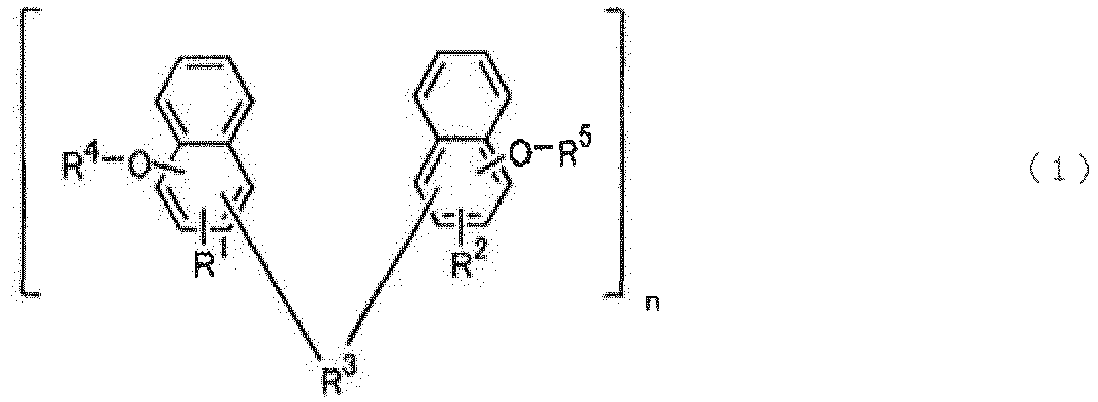


- An example of the fluorene compound includes a resin as follows, which is described in Japanese Unexamined Patent Application Publication No.
2008-274250 
- Examples of the naphthalene compound include resins as follows, which are described in Japanese Unexamined Patent Application Publication Nos.
2004-264710 2005-043471 2005-250434 2007-293294 2008-65303 


- Examples of the naphthol compound include resins as follows, which are described in Japanese Unexamined Patent Application Publication Nos.
2004-205685 2007-171895 2009-14816 


- Besides, the examples of the organic underlayer film include resins and compositions described in
WO2007-105776 ,WO2009-72465 WO2010-61774 WO2010-147155 ,WO2011-125839 ,WO2012-50064 WO2012-77640 WO2013-5797 WO2013-47106 WO2013-47516 WO2013-80929 WO2013-115097 ,WO2013-146670 ,WO2014-24836 WO2014-208324 ,WO2014-208499 ,WO2015-170736 ,WO2015-194273 ,WO2016-147989 , Japanese Unexamined Patent Application Publication Nos.2001-40293 2002-214777 2002-296789 2005-128509 2006-259249 2006-285046 2008-65081 2009-229666 2009-251130 2010-15112 2010-271654 2011-107684 2011-170059 2012-1687 2012-77295 2012-214720 2012-215842 2013-83939 2014-24831 2014-157169 2015-131954 2015-183046 2016-29160 2016-44272 2016-60886 2016-145849 2016-167047 2016-216367 2017-3959 2017-119670 2017-119671 2013-516643 2015-515112 - The silicon-containing middle layer film (silicon-containing, coating-type middle layer film) used in the inventive patterning process is not particularly limited. Many silicon-containing middle layer films usable herein are known. In the present invention, in the case where the organic underlayer film pattern has the silicon-containing middle layer film remaining on the organic underlayer film, the dry-etched silicon-containing film residue and the organic underlayer film need to be simultaneously removed by washing with a stripping liquid. For this reason, the silicon content in the silicon-containing middle layer film is preferably 40 weight% or less, more preferably 35 weight% or less, and particularly preferably 30 weight% or less.
- Moreover, the silicon-containing middle layer film is preferably formed from a composition for forming a silicon middle layer (the silicon-containing middle layer film), the composition containing a compound having a crosslinking organic structure.
- Such a composition makes the resulting silicon-containing middle layer film more surely removable simultaneously with the organic underlayer film by the washing with the stripping liquid after the dry etching.
- In this event, the crosslinking organic structure preferably include one or more selected from an oxirane ring, an oxetane ring, a hydroxyl group, or a carboxyl group.
- Such a crosslinking organic structure makes the silicon-containing middle layer film further surely removable simultaneously with the organic underlayer film by the washing with the stripping liquid after the dry etching.
- Moreover, the composition for forming a silicon middle layer preferably further contains an acid generator which generates an acid by one or both of heat and light.
- Additionally, the composition for forming a silicon middle layer preferably further contains a crosslinking agent.
- Such a composition(s) for forming a silicon middle layer promote crosslinking of the oxirane ring, oxetane ring, hydroxyl group, carboxyl group, or the like incorporated in the crosslinking organic structure. Furthermore, the composition makes it possible to form the silicon-containing middle layer film that is surely removable by the washing simultaneously with the organic underlayer film even after the dry etching.
- The compositions for forming a silicon middle layer as described above and resins used in the compositions are not particularly limited. Examples thereof include compositions and resins described in Japanese Unexamined Patent Application Publication Nos.
2004-310019 2005-15779 2005-18054 2005-352104 2007-226170 - Specific examples of the resins contained in the compositions for forming a silicon middle layer used in the present invention include polysiloxanes containing one or more of a compound shown by the following general formula (A-1), a hydrolysate, a condensate, and a hydrolysis condensate thereof.
R1A A1R2A A2R3A A3Si(OR0A)(4-A1-A2-A3) (A-1)
In the formula, R0A represents a hydrocarbon group having 1 to 6 carbon atoms; R1A, R2A, and R3A each represent a hydrogen atom or a monovalent organic group; and A1, A2, A3 each represent 0 or 1 while satisfying 0≤A1+A2+A3≤3. - Other examples of the organic group represented by R1A, R2A, and R3A include organic groups having at least one carbon-oxygen single bond or carbon-oxygen double bond. Specific examples thereof include organic groups having one or more moieties selected from the group consisting of an oxirane ring, an oxetane ring, an ester bond, an alkoxy group, and a hydroxyl group. An example of such organic groups includes one shown by the following general formula (A-2).
(P-Q1-(S1)v1-Q2-)u-(T)v2-Q3-(S2)v3-Q4- (A-2)
In the general formula (A-2), P represents a hydrogen atom, an oxirane ring, an oxetane ring, a hydroxyl group, an alkoxy group having 1 to 4 carbon atoms, an alkylcarbonyloxy group having 1 to 6 carbon atoms, or an alkylcarbonyl group having 1 to 6 carbon atoms; Q1, Q2, Q3, and Q4 each independently represent -CqH(2q-p)Pp-, where P is as defined above, "p" represents an integer of 0 to 3, and "q" represents an integer of 0 to 10, given that q=0 means a single bond; "u" represents an integer of 0 to 3; S1 and S2 each independently represent -O-, -CO-, -OCO-, -COO-, or -OCOO-; v1, v2, and v3 each independently represent 0 or 1. In addition to these, T represents a divalent group of an alicyclic or aromatic ring optionally containing a hetero atom, an oxirane ring, and an oxetane ring. Examples of the alicyclic or aromatic ring of T optionally containing a hetero atom such as an oxygen atom will be shown later. In T, positions where T bonds to Q2 and Q3 are not particularly limited, and can be appropriately selected by considering reactivity attributable to a steric factor, availability of a commercial reagent used in the reaction, and so on. - The upper layer resist film usable in the inventive patterning process is not particularly limited, and any of various conventionally known resist films is usable.
- Further, when the upper layer resist pattern is formed, if the upper layer resist needs a top coat to employ immersion exposure, a water-repellent coating film may be further formed on the upper layer resist film. The water-repellent coating film is not particularly limited, and various water-repellent coating films are usable.
- The step (2) is a step of subjecting the upper layer resist film to exposure and development to form an upper layer resist pattern.
- In the step (2), the upper layer resist film is subjected to pattern exposure according to a conventional method by adopting a light source based on this resist film, for example, a KrF excimer laser beam or ArF excimer laser beam. Further, the upper layer resist film is subjected to a heat treatment under conditions based on the individual resist films. Then, a development operation with a developer is performed, and the resist pattern can be obtained.
- The step (3) is a step of transferring the upper layer resist pattern to the silicon-containing middle layer film by dry etching using the upper layer resist film having the formed upper layer resist pattern as a mask, and further transferring the upper layer resist pattern to the organic underlayer film by dry etching using the silicon-containing middle layer film having the transferred upper layer resist pattern as a mask to form an organic underlayer film pattern.
- In the step (3), when the silicon-containing middle layer film is etched using the upper layer resist pattern as an etching mask under a dry etching condition where the etching speed of the silicon-containing middle layer film is significantly high relative to the organic underlayer film, for example, when dry etching is performed with fluorine-based gas plasma, this enables the silicon-containing middle layer film to have the upper layer resist pattern with little influence from the pattern change due to side etching of the resist film.
- Next, the organic underlayer film is etched under a dry etching condition where the etching speed of the organic underlayer film is significantly high relative to the substrate having the silicon-containing middle layer film with the transferred upper layer resist pattern, for example, reactive dry etching is performed with gas plasma containing oxygen or with gas plasma containing hydrogen and nitrogen.
- The organic underlayer film pattern is obtained by this etching step. Nevertheless, although the resist layer located uppermost is normally lost simultaneously with this step, a portion of the silicon-containing middle layer film served as the etching mask may be left on the upper portion of the organic underlayer film pattern as described below.
- In the step (3), the organic underlayer film pattern may have the silicon-containing middle layer film remaining on the organic underlayer film.
- Alternatively, in the step (3), the organic underlayer film pattern may not have the silicon-containing middle layer film remaining on the organic underlayer film.
- In the inventive patterning process, even when the material having served as the mask remains or does not remain after the pattern is transferred by the dry etching, the inorganic silicon film pattern (sidewall pattern) can be formed without damaging the sidewalls and the substrate.
- Note that when a pattern is transferred through multiple resist layers by dry etching which is actually employed in the process of manufacturing a semiconductor device, the rectangular shape of the pattern after the dry etching is ensured by setting such a condition that a portion of a patterned material serving as a mask is left on an upper portion of the transferred pattern in many cases. Specifically, in the inventive patterning process also, when the pattern is transferred to the silicon-containing middle layer film by dry etching using the upper layer resist as a mask, the step can be advanced under such a condition that a portion of the upper layer resist is left in order to ensure the rectangular shape of the cross section of the pattern of the silicon-containing middle layer film. Next, when the pattern is transferred to the organic underlayer film using the silicon-containing middle layer film as a mask also, the pattern transferring step can be advanced similarly in such a state that a portion of the silicon-containing middle layer film is left on the upper portion of the organic underlayer film to ensure the rectangular shape of the cross section of the pattern of the organic underlayer film. Then, the resulting organic underlayer film pattern is used as a core material in a sidewall spacer method, that is, after sidewalls are formed using the inorganic silicon film, the organic underlayer film pattern is removed to form the inorganic silicon film pattern. However, when the residue of the silicon-containing middle layer film remaining on the upper portion of the organic underlayer film pattern is to be removed by dry etching, the sidewalls formed of the inorganic silicon film and the substrate are damaged by the dry etching, resulting in the problems of poor product performance and yield decrease. Accordingly, in the inventive patterning process, wet processing is performed using a stripping liquid, as will be described later, to remove the silicon-containing middle layer film, so that such problems can be prevented.
- The step (4) is a step of forming an inorganic silicon film by a CVD method or an ALD method so as to cover the organic underlayer film pattern.
- In this event, the inorganic silicon film is not particularly limited. Preferable examples thereof include polysilicon, amorphous silicon, silicon oxide, silicon nitride, silicon oxynitride, silicon carbide, and composite materials thereof.
- The step (5) is a step of removing a portion of the inorganic silicon film by dry etching to expose an upper portion of the organic underlayer film pattern.
- The dry etching conditions in this event are not particularly limited. Depending on the composition of the inorganic silicon film, the gas condition and so forth can be determined.
- The step (6) is a step of removing the organic underlayer film pattern with a stripping liquid to form an inorganic silicon film pattern whose pattern pitch is 1/2 of that of the upper layer resist pattern.
- Additionally, in the step (6), the stripping liquid preferably contains one or both of hydrogen peroxide and sulfuric acid.
- For example, Japanese Unexamined Patent Application Publication No.
2009-212163 - In the step (6) in the present invention, the organic underlayer film pattern can be removed simultaneously with the silicon-containing film residue, if remaining thereon, by using a stripping liquid. For the wet stripping of the organic underlayer film pattern, it is more preferable to use the stripping liquid containing hydrogen peroxide. In this event, an acid or an alkali is further preferably added to adjust the pH to promote the stripping. Examples of the pH adjuster include inorganic acids such as hydrochloric acid and sulfuric acid; organic acids such as acetic acid, oxalic acid, tartaric acid, citric acid, and lactic acid; nitrogen-containing alkalis such as ammonia, ethanolamine, and tetramethylammonium hydroxide; nitrogen-containing organic acid compounds such as EDTA (ethylenediamine tetraacetic acid); and the like.
- The stripping liquid is normally an aqueous solution, but may contain an organic solvent in some cases. This organic solvent includes water-soluble alcohols, ethers, ketones, esters, amides, imides, and the like. Specific examples thereof includes methanol, ethanol, propanol, butanol, ethylene glycol, propylene glycol, diethylene glycol, dipropylene glycol, ethylene glycol methyl ether, ethylene glycol dimethyl ether, ethylene glycol ethyl ether, ethylene glycol diethyl ether, diethylene glycol methyl ether, diethylene glycol dimethyl ether, diethylene glycol ethyl ether, diethylene glycol diethyl ether, propylene glycol methyl ether, propylene glycol dimethyl ether, propylene glycol ethyl ether, propylene glycol diethyl ether, dipropylene glycol methyl ether, dipropylene glycol dimethyl ether, dipropylene glycol ethyl ether, dipropylene glycol diethyl ether, tetrahydrofuran, tetrahydrofurfuryl alcohol, acetone, methyl ethyl ketone, ethyl lactate, N-methylpyrrolidinone, N,N-dimethyl formamide, N,N-dimethylacetamide, and the like.
- The wet stripping can be performed only by: preparing a stripping liquid at 0°C to 200°C, preferably 20°C to 180°C; and immersing therein a silicon wafer having a target substrate to be processed. Furthermore, if necessary, the organic film pattern can be readily removed according to a conventional procedure such as spraying the stripping liquid onto the surface, or applying the stripping liquid thereto while the wafer is being rotated.
- Hereinafter, the present invention will be specifically described with reference to Examples and Comparative Example. However, the present invention is not limited thereto.
- As the organic underlayer film on the substrate, ODL-306 manufactured by Shin-Etsu Chemical Co., Ltd. was used and applied onto a Si wafer by spin-coating. After baking at 350°C for 60 seconds, a carbon film having a thickness of 80 nm was prepared. The carbon proportion of the carbon film was 88%. The silicon-containing middle layer film was prepared on the carbon film using a composition including the following raw materials. Specifically, the composition was applied onto the organic underlayer film by spin-coating and baked at 200°C for 60 seconds to prepare the silicon-containing middle layer film having a thickness of 30 nm.
-

-

- Further, an upper layer resist film having the following composition was applied onto the silicon-containing middle layer film by spin-coating, and baked at 110°C for 60 seconds. Thereby, the resist film had a thickness of 120 nm.
- Molecular weight (Mw)=8,100
Dispersity (Mw/Mn)=1.77
-

-

- The resultant was subjected to exposure using an ArF excimer laser scanner (NSR-S307E manufactured by Nikon Corporation, NA: 0.85, σ: 0.93/0.69, 20° dipole illumination, 6% halftone phase shift mask). Immediately after the photo-exposure, the resultant was baked at 100°C for 60 seconds and subjected to development with a 2.38 mass% tetramethylammonium hydroxide aqueous solution for 30 seconds. Thus, a positive isolated pattern (resist pattern) with a dimension of 50 nm and a pitch of 130 nm was obtained.
- Using the resist pattern as a mask, the silicon-containing middle layer film was processed by dry etching under the following conditions (1). Then, the pattern was transferred to the organic underlayer film under the following conditions (2).
-
Etching conditions (1): Chamber pressure 10 Pa Upper/Lower RF power 500 W/300 W CHF3 gas flow rate 50 ml/min CF4 gas flow rate 150 ml/min Ar gas flow rate 100 ml/min Treatment time 40 sec -
Etching conditions (2): Chamber pressure 2 Pa Upper/Lower RF power 1000 W/300 W O2 gas flow rate 300 ml/min N2 gas flow rate 100 ml/min Ar gas flow rate 100 ml/min Treatment time 30 sec - On the obtained organic underlayer film pattern, a silicon oxide film (ALD film) with a thickness of 30 nm was formed according to the method described from [0043] to [0053] in Example of Japanese Unexamined Patent Application Publication No.
2005-197561 -
Etching conditions (3): Chamber pressure 10 Pa Upper/Lower RF power 200 W/100 W CHF3 gas flow rate 50 ml/min CF4 gas flow rate 50 ml/min Ar gas flow rate 100 ml/min Treatment time 20 sec - The obtained test wafer A was treated with a sulfuric acid-hydrogen peroxide solution (H2SO4/H2O2/H2O=96/1/3), and then the cross-sectional shape was observed with S-4700 manufactured by Hitachi High-Technologies Corporation. The result verified that the sidewall pattern and the substrate were not damaged when the core material was removed.
- Similarly, the above-described treatments were performed, except that the silicon-containing middle layer film was prepared using a composition including the following raw materials. No damage to the sidewall pattern and the substrate was verified.
-

-

- The test wafer A obtained in Example 1 was treated under the following dry etching conditions to remove the core material. The result verified that the sidewall pattern and the substrate were damaged when the core pattern was removed.
-
Etching conditions (4): Chamber pressure 5 Pa Upper/Lower RF power 1000 W/300 W O2 gas flow rate 300 ml/min N2 gas flow rate 100 ml/min Ar gas flow rate 100 ml/min Treatment time 30 sec - From the above results, in Examples employing the inventive patterning process, the sidewall patterns and the substrates were not damaged by removing the core patterns. This revealed that the inventive patterning process is capable of solving the problems of poor product performance and yield decrease. Meanwhile, in Comparative Example, not the wet processing but the dry etching was employed when the core pattern was removed. Consequently, the sidewall pattern and the substrate were damaged.
- It should be noted that the present invention is not limited to the above-described embodiments. The embodiments are just examples, and any examples that have substantially the same feature and demonstrate the same functions and effects as those in the technical concept disclosed in claims of the present invention are included in the technical scope of the present invention.
Claims (10)
- A patterning process comprising the steps of:(1) forming on a substrate an organic underlayer film, a silicon-containing middle layer film thereon, and further an upper layer resist film thereon;(2) subjecting the upper layer resist film to exposure and development to form an upper layer resist pattern;(3) transferring the upper layer resist pattern to the silicon-containing middle layer film by dry etching using the upper layer resist film having the formed upper layer resist pattern as a mask, and further transferring the upper layer resist pattern to the organic underlayer film by dry etching using the silicon-containing middle layer film having the transferred upper layer resist pattern as a mask to form an organic underlayer film pattern;(4) forming an inorganic silicon film by a CVD method or an ALD method so as to cover the organic underlayer film pattern;(5) removing a portion of the inorganic silicon film by dry etching to expose an upper portion of the organic underlayer film pattern; and(6) removing the organic underlayer film pattern with a stripping liquid to form an inorganic silicon film pattern whose pattern pitch is 1/2 of that of the upper layer resist pattern.
- The patterning process according to claim 1, wherein the inorganic silicon film is made of polysilicon, amorphous silicon, silicon oxide, silicon nitride, silicon oxynitride, silicon carbide, or a composite material thereof.
- The patterning process according to claim 1 or 2, wherein, in the step (1), a water-repellent coating film is further formed on the upper layer resist film.
- The patterning process according to any one of claims 1 to 3, wherein, in the step (3), the organic underlayer film pattern has the silicon-containing middle layer film remaining on the organic underlayer film.
- The patterning process according to any one of claims 1 to 3, wherein, in the step (3), the organic underlayer film pattern does not have the silicon-containing middle layer film remaining on the organic underlayer film.
- The patterning process according to any one of claims 1 to 5, wherein, in the step (6), the stripping liquid contains one or both of hydrogen peroxide and sulfuric acid.
- The patterning process according to any one of claims 1 to 6, wherein the silicon-containing middle layer film is formed from a composition for forming a silicon middle layer, the composition containing a compound having a crosslinking organic structure.
- The patterning process according to claim 7, wherein the crosslinking organic structure is one or more selected from an oxirane ring, an oxetane ring, a hydroxyl group, or a carboxyl group.
- The patterning process according to claim 7 or 8, wherein the composition for forming a silicon middle layer further contains an acid generator which generates an acid by one or both of heat and light.
- The patterning process according to any one of claims 7 to 9, wherein the composition for forming a silicon middle layer further contains a crosslinking agent.
Applications Claiming Priority (1)
| Application Number | Priority Date | Filing Date | Title |
|---|---|---|---|
| JP2018171333A JP6981945B2 (en) | 2018-09-13 | 2018-09-13 | Pattern formation method |
Publications (2)
| Publication Number | Publication Date |
|---|---|
| EP3623867A1 true EP3623867A1 (en) | 2020-03-18 |
| EP3623867B1 EP3623867B1 (en) | 2024-08-14 |
Family
ID=67734543
Family Applications (1)
| Application Number | Title | Priority Date | Filing Date |
|---|---|---|---|
| EP19193091.6A Active EP3623867B1 (en) | 2018-09-13 | 2019-08-22 | Patterning process |
Country Status (6)
| Country | Link |
|---|---|
| US (1) | US20200090935A1 (en) |
| EP (1) | EP3623867B1 (en) |
| JP (1) | JP6981945B2 (en) |
| KR (1) | KR102290945B1 (en) |
| CN (1) | CN110895380A (en) |
| TW (1) | TWI722561B (en) |
Cited By (2)
| Publication number | Priority date | Publication date | Assignee | Title |
|---|---|---|---|---|
| EP4369100A1 (en) * | 2022-11-08 | 2024-05-15 | Shin-Etsu Chemical Co., Ltd. | Compound for forming metal-containing film, composition for forming metal-containing film, and patterning process |
| EP4660706A3 (en) * | 2024-05-29 | 2025-12-24 | Shin-Etsu Chemical Co., Ltd. | Patterning process |
Families Citing this family (4)
| Publication number | Priority date | Publication date | Assignee | Title |
|---|---|---|---|---|
| US20220091513A1 (en) * | 2020-09-18 | 2022-03-24 | Applied Materials, Inc. | Film structure for electric field assisted bake process |
| JP7611785B2 (en) * | 2021-07-06 | 2025-01-10 | 信越化学工業株式会社 | Adhesion film forming material, method for forming adhesion film using same, and method for forming pattern using adhesion film forming material |
| CN113725081B (en) * | 2021-08-30 | 2024-08-06 | 上海华力微电子有限公司 | Method for improving photoetching development defect of NAND flash active region |
| JP7856592B2 (en) * | 2023-02-15 | 2026-05-11 | 信越化学工業株式会社 | Pattern formation method |
Citations (76)
| Publication number | Priority date | Publication date | Assignee | Title |
|---|---|---|---|---|
| JP2001040293A (en) | 1999-08-03 | 2001-02-13 | Jsr Corp | Antireflection film forming composition |
| JP2002214777A (en) | 2000-11-14 | 2002-07-31 | Jsr Corp | Antireflection film forming composition |
| JP2002296789A (en) | 2001-03-29 | 2002-10-09 | Jsr Corp | Composition for forming lower layer film for multilayered resist process |
| JP2004205685A (en) | 2002-12-24 | 2004-07-22 | Shin Etsu Chem Co Ltd | Pattern forming method and underlayer film forming material |
| JP2004264710A (en) | 2003-03-04 | 2004-09-24 | Jsr Corp | Antireflection film forming composition and antireflection film |
| JP2004310019A (en) | 2003-03-24 | 2004-11-04 | Shin Etsu Chem Co Ltd | Antireflection film material, substrate having antireflection film, and pattern forming method |
| JP2005015779A (en) | 2003-06-03 | 2005-01-20 | Shin Etsu Chem Co Ltd | Antireflection film material, antireflection film using the same, and pattern forming method |
| JP2005018054A (en) | 2003-06-03 | 2005-01-20 | Shin Etsu Chem Co Ltd | Antireflection film material, antireflection film using the same, and pattern forming method |
| JP2005043471A (en) | 2003-07-23 | 2005-02-17 | Jsr Corp | Antireflection film forming composition and method for forming antireflection film |
| JP2005128509A (en) | 2003-10-03 | 2005-05-19 | Shin Etsu Chem Co Ltd | Photoresist underlayer film forming material and pattern forming method |
| JP2005197561A (en) | 2004-01-09 | 2005-07-21 | Hitachi Kokusai Electric Inc | Substrate processing equipment |
| JP2005250434A (en) | 2004-02-04 | 2005-09-15 | Shin Etsu Chem Co Ltd | Resist underlayer film material and pattern forming method |
| JP2005352104A (en) | 2004-06-10 | 2005-12-22 | Shin Etsu Chem Co Ltd | Anti-reflective coating material and method of manufacturing the same, anti-reflective coating using the same, and pattern formation |
| JP2006259249A (en) | 2005-03-17 | 2006-09-28 | Shin Etsu Chem Co Ltd | Photoresist underlayer film forming material and pattern forming method |
| JP2006285046A (en) | 2005-04-01 | 2006-10-19 | Jsr Corp | Composition for resist underlayer film |
| US20060281266A1 (en) * | 2005-06-09 | 2006-12-14 | Wells David H | Method and apparatus for adjusting feature size and position |
| JP2007171895A (en) | 2005-11-28 | 2007-07-05 | Shin Etsu Chem Co Ltd | Resist underlayer film material and pattern forming method |
| JP2007199653A (en) | 2005-12-27 | 2007-08-09 | Shin Etsu Chem Co Ltd | Photoresist underlayer film forming material and pattern forming method |
| JP2007226170A (en) | 2006-01-27 | 2007-09-06 | Shin Etsu Chem Co Ltd | Antireflection film material, substrate having antireflection film, and pattern forming method |
| WO2007105776A1 (en) | 2006-03-14 | 2007-09-20 | Jsr Corporation | Composition for forming lower layer film and pattern forming method |
| JP2007293294A (en) | 2006-03-27 | 2007-11-08 | Jsr Corp | Fine pattern forming method and polymer |
| JP2008033174A (en) | 2006-07-31 | 2008-02-14 | Tokyo Ohka Kogyo Co Ltd | Pattern forming method, metal oxide film forming material and method of using the same |
| JP2008065081A (en) | 2006-09-07 | 2008-03-21 | Jsr Corp | Resist underlayer film forming composition and pattern forming method |
| JP2008065303A (en) | 2006-08-10 | 2008-03-21 | Shin Etsu Chem Co Ltd | Resist underlayer film material and pattern forming method |
| JP2008274250A (en) | 2007-04-06 | 2008-11-13 | Osaka Gas Co Ltd | Phenolic resin and method for producing the same |
| JP2009014816A (en) | 2007-07-02 | 2009-01-22 | Jsr Corp | Resist underlayer film forming composition and pattern forming method |
| WO2009072465A1 (en) | 2007-12-07 | 2009-06-11 | Mitsubishi Gas Chemical Company, Inc. | Composition for forming base film for lithography and method for forming multilayer resist pattern |
| US20090163030A1 (en) * | 2007-12-18 | 2009-06-25 | Mitsuhiro Omura | Semiconductor device manufacturing method |
| JP2009212163A (en) | 2008-02-29 | 2009-09-17 | Toshiba Corp | Method of fabricating semiconductor device |
| JP2009229666A (en) | 2008-03-21 | 2009-10-08 | Jsr Corp | Composition for forming lower layer film and pattern forming method using the same |
| JP2009251130A (en) | 2008-04-02 | 2009-10-29 | Jsr Corp | Composition for resist lower-layer film formation, and method of forming dual-damascene structure using the same |
| JP2010015112A (en) | 2008-07-07 | 2010-01-21 | Jsr Corp | Underlayer film forming composition for multilayer resist process |
| JP2010122656A (en) | 2008-10-20 | 2010-06-03 | Shin-Etsu Chemical Co Ltd | Method for forming resist underlayer film, patterning process using the same, and resist underlayer film material |
| WO2010061774A1 (en) | 2008-11-27 | 2010-06-03 | 日産化学工業株式会社 | Composition for forming resist underlayer film with reduced outgassing |
| JP2010271654A (en) | 2009-05-25 | 2010-12-02 | Shin-Etsu Chemical Co Ltd | Resist underlayer film material and pattern forming method using the same |
| WO2010147155A1 (en) | 2009-06-19 | 2010-12-23 | 日産化学工業株式会社 | Carbazole novolak resin |
| JP2011107684A (en) | 2009-11-13 | 2011-06-02 | Cheil Industries Inc | Resist underlayer polymer, resist underlayer composition including the same, and method of pattering element |
| JP2011170059A (en) | 2010-02-18 | 2011-09-01 | Jsr Corp | Resist underlayer film forming method, pattern forming method and composition, additive for resist underlayer film forming material, crosslinking agent, and resist underlayer film |
| WO2011125839A1 (en) | 2010-03-31 | 2011-10-13 | Jsr株式会社 | Composition for forming resist underlayer film and pattern forming method |
| JP2012001687A (en) | 2010-06-21 | 2012-01-05 | Shin-Etsu Chemical Co Ltd | Naphthalene derivative, resist underlayer film material, resist underlayer film forming method, and pattern forming method |
| JP2012077295A (en) | 2010-09-10 | 2012-04-19 | Shin-Etsu Chemical Co Ltd | Naphthalene derivative and method for preparing the same, resist bottom layer material, method for forming resist bottom layer, and patterning process |
| WO2012050064A1 (en) | 2010-10-14 | 2012-04-19 | 日産化学工業株式会社 | Lithographic resist underlayer film-forming compound that comprises resin including polyether structure |
| WO2012077640A1 (en) | 2010-12-09 | 2012-06-14 | 日産化学工業株式会社 | Composition for forming resist underlayer film containing hydroxyl group-containing carbazole novolac resin |
| JP2012214720A (en) | 2011-03-28 | 2012-11-08 | Shin-Etsu Chemical Co Ltd | Biphenyl derivative, resist lower layer film material, method for forming resist lower layer film, and method for forming pattern |
| JP2012215842A (en) | 2011-03-31 | 2012-11-08 | Jsr Corp | Composition for forming resist underlay film and pattern forming method |
| WO2013005797A1 (en) | 2011-07-07 | 2013-01-10 | 日産化学工業株式会社 | Resist underlayer film-forming composition which contains alicyclic skeleton-containing carbazole resin |
| US20130034963A1 (en) * | 2011-08-02 | 2013-02-07 | Chung Byung-Hong | Methods of forming fine patterns for semiconductor device |
| WO2013047516A1 (en) | 2011-09-29 | 2013-04-04 | 日産化学工業株式会社 | Diarylamine novolac resin |
| WO2013047106A1 (en) | 2011-09-30 | 2013-04-04 | 三菱瓦斯化学株式会社 | Resin having fluorene structure and underlayer film-forming material for lithography |
| JP2013083939A (en) | 2011-09-30 | 2013-05-09 | Jsr Corp | Composition for forming resist underlayer film, resist underlayer film and method for forming the same, and method for forming pattern |
| JP2013516643A (en) | 2009-12-31 | 2013-05-13 | チェイル インダストリーズ インコーポレイテッド | Aromatic ring-containing polymer for resist underlayer film and resist underlayer film composition containing the same |
| WO2013080929A1 (en) | 2011-12-01 | 2013-06-06 | Jsr株式会社 | Resist-underlayer-film-forming composition used in multilayer resist process, resist underlayer film, method for forming same, and pattern-formation method |
| WO2013115097A1 (en) | 2012-02-01 | 2013-08-08 | 日産化学工業株式会社 | Resist underlayer film forming composition containing copolymer resin having heterocyclic ring |
| WO2013146670A1 (en) | 2012-03-27 | 2013-10-03 | 日産化学工業株式会社 | Resist underlayer film-forming composition which contains phenylindole-containing novolac resin |
| JP2014024831A (en) | 2012-06-18 | 2014-02-06 | Shin Etsu Chem Co Ltd | Compound for forming organic film, and organic film material using the same, process for forming organic film, and patterning process |
| WO2014024836A1 (en) | 2012-08-10 | 2014-02-13 | 日産化学工業株式会社 | Composition for forming resist underlayer film |
| JP2014157169A (en) | 2011-06-24 | 2014-08-28 | Nissan Chem Ind Ltd | Composition for forming resist underlay film containing polyhydroxybenzene novolak resin |
| WO2014208324A1 (en) | 2013-06-24 | 2014-12-31 | Jsr株式会社 | Composition for film formation use, resist underlayer film and method for formation thereof, pattern formation method, and compound |
| WO2014208499A1 (en) | 2013-06-25 | 2014-12-31 | 日産化学工業株式会社 | Resist underlayer film forming composition containing pyrrole novolac resin |
| JP2015515112A (en) | 2011-12-30 | 2015-05-21 | チェイル インダストリーズ インコーポレイテッド | Monomer for hard mask composition, hard mask composition containing the monomer, and pattern forming method using the hard mask composition |
| JP2015131954A (en) | 2013-12-12 | 2015-07-23 | ローム アンド ハース エレクトロニック マテリアルズ エルエルシーRohm and Haas Electronic Materials LLC | Aromatic resins for underlayers |
| JP2015183046A (en) | 2014-03-20 | 2015-10-22 | Jsr株式会社 | Film forming composition, resist underlayer film, method for forming the same, and pattern forming method |
| WO2015170736A1 (en) | 2014-05-08 | 2015-11-12 | 三菱瓦斯化学株式会社 | Lithographic film formation material, composition for lithographic film formation, lithographic film, pattern formation method, and purification method |
| WO2015194273A1 (en) | 2014-06-16 | 2015-12-23 | 日産化学工業株式会社 | Resist underlayer film-forming composition |
| JP2016029160A (en) | 2014-07-15 | 2016-03-03 | ローム アンド ハース エレクトロニック マテリアルズ エルエルシーRohm and Haas Electronic Materials LLC | Resin for underlayer |
| JP2016044272A (en) | 2014-08-25 | 2016-04-04 | Jsr株式会社 | Composition for forming film, film and manufacturing method and compound of substrate having formed pattern |
| JP2016060886A (en) | 2014-09-19 | 2016-04-25 | Jsr株式会社 | Composition for forming film, film, method for manufacturing patterned substrate, and compound |
| JP2016145849A (en) | 2013-06-17 | 2016-08-12 | 日産化学工業株式会社 | Resist underlayer film forming composition containing trihydroxynaphthalene novolak resin |
| JP2016167047A (en) | 2015-03-03 | 2016-09-15 | Jsr株式会社 | Composition for forming resist underlayer film, resist underlayer film and patterned substrate manufacturing method |
| WO2016147989A1 (en) | 2015-03-13 | 2016-09-22 | 三菱瓦斯化学株式会社 | Compound, resin, material for forming underlayer film for lithography, composition for forming underlayer film for lithography, underlayer film for lithography, pattern forming method, and method for purifying compound or resin |
| JP2016216367A (en) | 2015-05-14 | 2016-12-22 | 信越化学工業株式会社 | Organic film material, organic film formation method, pattern formation method, and compound |
| JP2017003959A (en) | 2015-06-04 | 2017-01-05 | 信越化学工業株式会社 | Resist underlay film material and pattern formation method |
| JP2017119671A (en) | 2015-12-24 | 2017-07-06 | 信越化学工業株式会社 | Compound for forming organic film, composition for forming organic film, method for forming organic film, and patterning process |
| JP2017119670A (en) | 2015-12-24 | 2017-07-06 | 信越化学工業株式会社 | Compound for forming organic film, composition for forming organic film, method for forming organic film, and patterning process |
| US20180158674A1 (en) * | 2016-12-05 | 2018-06-07 | Rohm And Haas Electronic Materials Llc | Aromatic resins for underlayers |
| EP3508918A1 (en) * | 2017-12-26 | 2019-07-10 | Shin-Etsu Chemical Co., Ltd. | Composition for forming organic film, substrate for manufacturing semiconductor device, method for forming organic film, and patterning process |
Family Cites Families (10)
| Publication number | Priority date | Publication date | Assignee | Title |
|---|---|---|---|---|
| JP4553113B2 (en) * | 2004-06-10 | 2010-09-29 | 信越化学工業株式会社 | Porous film-forming composition, pattern-forming method, and porous sacrificial film |
| JP2008058591A (en) * | 2006-08-31 | 2008-03-13 | Toshiba Corp | Substrate processing method and electronic device manufacturing method |
| CN101878451B (en) * | 2007-11-30 | 2013-04-24 | 日产化学工业株式会社 | Blocked isocyanato bearing silicon containing composition for the formation of resist undercoat |
| JP5015892B2 (en) * | 2008-10-02 | 2012-08-29 | 信越化学工業株式会社 | Silicon-containing film-forming composition, silicon-containing film-forming substrate, and pattern forming method |
| JP5453361B2 (en) * | 2011-08-17 | 2014-03-26 | 信越化学工業株式会社 | Silicon-containing resist underlayer film forming composition and pattern forming method |
| JP5833492B2 (en) * | 2012-04-23 | 2015-12-16 | 信越化学工業株式会社 | Silicon compound, polysiloxane compound, composition for forming resist underlayer film containing the same, and pattern forming method |
| US8759220B1 (en) * | 2013-02-28 | 2014-06-24 | Shin-Etsu Chemical Co., Ltd. | Patterning process |
| JP6114157B2 (en) * | 2013-10-02 | 2017-04-12 | 信越化学工業株式会社 | Silicon-containing resist underlayer film forming composition and pattern forming method |
| JP6243815B2 (en) * | 2014-09-01 | 2017-12-06 | 信越化学工業株式会社 | Manufacturing method of semiconductor device substrate |
| JP2018018038A (en) * | 2016-07-29 | 2018-02-01 | 富士フイルム株式会社 | Patterning method and method for manufacturing electronic device using the same |
-
2018
- 2018-09-13 JP JP2018171333A patent/JP6981945B2/en active Active
-
2019
- 2019-08-22 US US16/547,870 patent/US20200090935A1/en not_active Abandoned
- 2019-08-22 EP EP19193091.6A patent/EP3623867B1/en active Active
- 2019-09-10 TW TW108132501A patent/TWI722561B/en active
- 2019-09-10 KR KR1020190112073A patent/KR102290945B1/en active Active
- 2019-09-12 CN CN201910864595.8A patent/CN110895380A/en active Pending
Patent Citations (76)
| Publication number | Priority date | Publication date | Assignee | Title |
|---|---|---|---|---|
| JP2001040293A (en) | 1999-08-03 | 2001-02-13 | Jsr Corp | Antireflection film forming composition |
| JP2002214777A (en) | 2000-11-14 | 2002-07-31 | Jsr Corp | Antireflection film forming composition |
| JP2002296789A (en) | 2001-03-29 | 2002-10-09 | Jsr Corp | Composition for forming lower layer film for multilayered resist process |
| JP2004205685A (en) | 2002-12-24 | 2004-07-22 | Shin Etsu Chem Co Ltd | Pattern forming method and underlayer film forming material |
| JP2004264710A (en) | 2003-03-04 | 2004-09-24 | Jsr Corp | Antireflection film forming composition and antireflection film |
| JP2004310019A (en) | 2003-03-24 | 2004-11-04 | Shin Etsu Chem Co Ltd | Antireflection film material, substrate having antireflection film, and pattern forming method |
| JP2005015779A (en) | 2003-06-03 | 2005-01-20 | Shin Etsu Chem Co Ltd | Antireflection film material, antireflection film using the same, and pattern forming method |
| JP2005018054A (en) | 2003-06-03 | 2005-01-20 | Shin Etsu Chem Co Ltd | Antireflection film material, antireflection film using the same, and pattern forming method |
| JP2005043471A (en) | 2003-07-23 | 2005-02-17 | Jsr Corp | Antireflection film forming composition and method for forming antireflection film |
| JP2005128509A (en) | 2003-10-03 | 2005-05-19 | Shin Etsu Chem Co Ltd | Photoresist underlayer film forming material and pattern forming method |
| JP2005197561A (en) | 2004-01-09 | 2005-07-21 | Hitachi Kokusai Electric Inc | Substrate processing equipment |
| JP2005250434A (en) | 2004-02-04 | 2005-09-15 | Shin Etsu Chem Co Ltd | Resist underlayer film material and pattern forming method |
| JP2005352104A (en) | 2004-06-10 | 2005-12-22 | Shin Etsu Chem Co Ltd | Anti-reflective coating material and method of manufacturing the same, anti-reflective coating using the same, and pattern formation |
| JP2006259249A (en) | 2005-03-17 | 2006-09-28 | Shin Etsu Chem Co Ltd | Photoresist underlayer film forming material and pattern forming method |
| JP2006285046A (en) | 2005-04-01 | 2006-10-19 | Jsr Corp | Composition for resist underlayer film |
| US20060281266A1 (en) * | 2005-06-09 | 2006-12-14 | Wells David H | Method and apparatus for adjusting feature size and position |
| JP2007171895A (en) | 2005-11-28 | 2007-07-05 | Shin Etsu Chem Co Ltd | Resist underlayer film material and pattern forming method |
| JP2007199653A (en) | 2005-12-27 | 2007-08-09 | Shin Etsu Chem Co Ltd | Photoresist underlayer film forming material and pattern forming method |
| JP2007226170A (en) | 2006-01-27 | 2007-09-06 | Shin Etsu Chem Co Ltd | Antireflection film material, substrate having antireflection film, and pattern forming method |
| WO2007105776A1 (en) | 2006-03-14 | 2007-09-20 | Jsr Corporation | Composition for forming lower layer film and pattern forming method |
| JP2007293294A (en) | 2006-03-27 | 2007-11-08 | Jsr Corp | Fine pattern forming method and polymer |
| JP2008033174A (en) | 2006-07-31 | 2008-02-14 | Tokyo Ohka Kogyo Co Ltd | Pattern forming method, metal oxide film forming material and method of using the same |
| JP2008065303A (en) | 2006-08-10 | 2008-03-21 | Shin Etsu Chem Co Ltd | Resist underlayer film material and pattern forming method |
| JP2008065081A (en) | 2006-09-07 | 2008-03-21 | Jsr Corp | Resist underlayer film forming composition and pattern forming method |
| JP2008274250A (en) | 2007-04-06 | 2008-11-13 | Osaka Gas Co Ltd | Phenolic resin and method for producing the same |
| JP2009014816A (en) | 2007-07-02 | 2009-01-22 | Jsr Corp | Resist underlayer film forming composition and pattern forming method |
| WO2009072465A1 (en) | 2007-12-07 | 2009-06-11 | Mitsubishi Gas Chemical Company, Inc. | Composition for forming base film for lithography and method for forming multilayer resist pattern |
| US20090163030A1 (en) * | 2007-12-18 | 2009-06-25 | Mitsuhiro Omura | Semiconductor device manufacturing method |
| JP2009212163A (en) | 2008-02-29 | 2009-09-17 | Toshiba Corp | Method of fabricating semiconductor device |
| JP2009229666A (en) | 2008-03-21 | 2009-10-08 | Jsr Corp | Composition for forming lower layer film and pattern forming method using the same |
| JP2009251130A (en) | 2008-04-02 | 2009-10-29 | Jsr Corp | Composition for resist lower-layer film formation, and method of forming dual-damascene structure using the same |
| JP2010015112A (en) | 2008-07-07 | 2010-01-21 | Jsr Corp | Underlayer film forming composition for multilayer resist process |
| JP2010122656A (en) | 2008-10-20 | 2010-06-03 | Shin-Etsu Chemical Co Ltd | Method for forming resist underlayer film, patterning process using the same, and resist underlayer film material |
| WO2010061774A1 (en) | 2008-11-27 | 2010-06-03 | 日産化学工業株式会社 | Composition for forming resist underlayer film with reduced outgassing |
| JP2010271654A (en) | 2009-05-25 | 2010-12-02 | Shin-Etsu Chemical Co Ltd | Resist underlayer film material and pattern forming method using the same |
| WO2010147155A1 (en) | 2009-06-19 | 2010-12-23 | 日産化学工業株式会社 | Carbazole novolak resin |
| JP2011107684A (en) | 2009-11-13 | 2011-06-02 | Cheil Industries Inc | Resist underlayer polymer, resist underlayer composition including the same, and method of pattering element |
| JP2013516643A (en) | 2009-12-31 | 2013-05-13 | チェイル インダストリーズ インコーポレイテッド | Aromatic ring-containing polymer for resist underlayer film and resist underlayer film composition containing the same |
| JP2011170059A (en) | 2010-02-18 | 2011-09-01 | Jsr Corp | Resist underlayer film forming method, pattern forming method and composition, additive for resist underlayer film forming material, crosslinking agent, and resist underlayer film |
| WO2011125839A1 (en) | 2010-03-31 | 2011-10-13 | Jsr株式会社 | Composition for forming resist underlayer film and pattern forming method |
| JP2012001687A (en) | 2010-06-21 | 2012-01-05 | Shin-Etsu Chemical Co Ltd | Naphthalene derivative, resist underlayer film material, resist underlayer film forming method, and pattern forming method |
| JP2012077295A (en) | 2010-09-10 | 2012-04-19 | Shin-Etsu Chemical Co Ltd | Naphthalene derivative and method for preparing the same, resist bottom layer material, method for forming resist bottom layer, and patterning process |
| WO2012050064A1 (en) | 2010-10-14 | 2012-04-19 | 日産化学工業株式会社 | Lithographic resist underlayer film-forming compound that comprises resin including polyether structure |
| WO2012077640A1 (en) | 2010-12-09 | 2012-06-14 | 日産化学工業株式会社 | Composition for forming resist underlayer film containing hydroxyl group-containing carbazole novolac resin |
| JP2012214720A (en) | 2011-03-28 | 2012-11-08 | Shin-Etsu Chemical Co Ltd | Biphenyl derivative, resist lower layer film material, method for forming resist lower layer film, and method for forming pattern |
| JP2012215842A (en) | 2011-03-31 | 2012-11-08 | Jsr Corp | Composition for forming resist underlay film and pattern forming method |
| JP2014157169A (en) | 2011-06-24 | 2014-08-28 | Nissan Chem Ind Ltd | Composition for forming resist underlay film containing polyhydroxybenzene novolak resin |
| WO2013005797A1 (en) | 2011-07-07 | 2013-01-10 | 日産化学工業株式会社 | Resist underlayer film-forming composition which contains alicyclic skeleton-containing carbazole resin |
| US20130034963A1 (en) * | 2011-08-02 | 2013-02-07 | Chung Byung-Hong | Methods of forming fine patterns for semiconductor device |
| WO2013047516A1 (en) | 2011-09-29 | 2013-04-04 | 日産化学工業株式会社 | Diarylamine novolac resin |
| WO2013047106A1 (en) | 2011-09-30 | 2013-04-04 | 三菱瓦斯化学株式会社 | Resin having fluorene structure and underlayer film-forming material for lithography |
| JP2013083939A (en) | 2011-09-30 | 2013-05-09 | Jsr Corp | Composition for forming resist underlayer film, resist underlayer film and method for forming the same, and method for forming pattern |
| WO2013080929A1 (en) | 2011-12-01 | 2013-06-06 | Jsr株式会社 | Resist-underlayer-film-forming composition used in multilayer resist process, resist underlayer film, method for forming same, and pattern-formation method |
| JP2015515112A (en) | 2011-12-30 | 2015-05-21 | チェイル インダストリーズ インコーポレイテッド | Monomer for hard mask composition, hard mask composition containing the monomer, and pattern forming method using the hard mask composition |
| WO2013115097A1 (en) | 2012-02-01 | 2013-08-08 | 日産化学工業株式会社 | Resist underlayer film forming composition containing copolymer resin having heterocyclic ring |
| WO2013146670A1 (en) | 2012-03-27 | 2013-10-03 | 日産化学工業株式会社 | Resist underlayer film-forming composition which contains phenylindole-containing novolac resin |
| JP2014024831A (en) | 2012-06-18 | 2014-02-06 | Shin Etsu Chem Co Ltd | Compound for forming organic film, and organic film material using the same, process for forming organic film, and patterning process |
| WO2014024836A1 (en) | 2012-08-10 | 2014-02-13 | 日産化学工業株式会社 | Composition for forming resist underlayer film |
| JP2016145849A (en) | 2013-06-17 | 2016-08-12 | 日産化学工業株式会社 | Resist underlayer film forming composition containing trihydroxynaphthalene novolak resin |
| WO2014208324A1 (en) | 2013-06-24 | 2014-12-31 | Jsr株式会社 | Composition for film formation use, resist underlayer film and method for formation thereof, pattern formation method, and compound |
| WO2014208499A1 (en) | 2013-06-25 | 2014-12-31 | 日産化学工業株式会社 | Resist underlayer film forming composition containing pyrrole novolac resin |
| JP2015131954A (en) | 2013-12-12 | 2015-07-23 | ローム アンド ハース エレクトロニック マテリアルズ エルエルシーRohm and Haas Electronic Materials LLC | Aromatic resins for underlayers |
| JP2015183046A (en) | 2014-03-20 | 2015-10-22 | Jsr株式会社 | Film forming composition, resist underlayer film, method for forming the same, and pattern forming method |
| WO2015170736A1 (en) | 2014-05-08 | 2015-11-12 | 三菱瓦斯化学株式会社 | Lithographic film formation material, composition for lithographic film formation, lithographic film, pattern formation method, and purification method |
| WO2015194273A1 (en) | 2014-06-16 | 2015-12-23 | 日産化学工業株式会社 | Resist underlayer film-forming composition |
| JP2016029160A (en) | 2014-07-15 | 2016-03-03 | ローム アンド ハース エレクトロニック マテリアルズ エルエルシーRohm and Haas Electronic Materials LLC | Resin for underlayer |
| JP2016044272A (en) | 2014-08-25 | 2016-04-04 | Jsr株式会社 | Composition for forming film, film and manufacturing method and compound of substrate having formed pattern |
| JP2016060886A (en) | 2014-09-19 | 2016-04-25 | Jsr株式会社 | Composition for forming film, film, method for manufacturing patterned substrate, and compound |
| JP2016167047A (en) | 2015-03-03 | 2016-09-15 | Jsr株式会社 | Composition for forming resist underlayer film, resist underlayer film and patterned substrate manufacturing method |
| WO2016147989A1 (en) | 2015-03-13 | 2016-09-22 | 三菱瓦斯化学株式会社 | Compound, resin, material for forming underlayer film for lithography, composition for forming underlayer film for lithography, underlayer film for lithography, pattern forming method, and method for purifying compound or resin |
| JP2016216367A (en) | 2015-05-14 | 2016-12-22 | 信越化学工業株式会社 | Organic film material, organic film formation method, pattern formation method, and compound |
| JP2017003959A (en) | 2015-06-04 | 2017-01-05 | 信越化学工業株式会社 | Resist underlay film material and pattern formation method |
| JP2017119671A (en) | 2015-12-24 | 2017-07-06 | 信越化学工業株式会社 | Compound for forming organic film, composition for forming organic film, method for forming organic film, and patterning process |
| JP2017119670A (en) | 2015-12-24 | 2017-07-06 | 信越化学工業株式会社 | Compound for forming organic film, composition for forming organic film, method for forming organic film, and patterning process |
| US20180158674A1 (en) * | 2016-12-05 | 2018-06-07 | Rohm And Haas Electronic Materials Llc | Aromatic resins for underlayers |
| EP3508918A1 (en) * | 2017-12-26 | 2019-07-10 | Shin-Etsu Chemical Co., Ltd. | Composition for forming organic film, substrate for manufacturing semiconductor device, method for forming organic film, and patterning process |
Non-Patent Citations (3)
| Title |
|---|
| J. VAC. SCI. TECHNOL., vol. B17, no. 6, November 1999 (1999-11-01) |
| MEISSNER D ET AL: "Optical absorption of amorphous hydrogenated carbon thin films", THIN SOLID FILMS, ELSEVIER, AMSTERDAM, NL, vol. 283, no. 1, 1 September 1996 (1996-09-01), pages 196 - 203, XP004053665, ISSN: 0040-6090, DOI: 10.1016/0040-6090(95)08251-4 * |
| PROC. SPIE, vol. 5754, 2005, pages 1508 |
Cited By (2)
| Publication number | Priority date | Publication date | Assignee | Title |
|---|---|---|---|---|
| EP4369100A1 (en) * | 2022-11-08 | 2024-05-15 | Shin-Etsu Chemical Co., Ltd. | Compound for forming metal-containing film, composition for forming metal-containing film, and patterning process |
| EP4660706A3 (en) * | 2024-05-29 | 2025-12-24 | Shin-Etsu Chemical Co., Ltd. | Patterning process |
Also Published As
| Publication number | Publication date |
|---|---|
| JP6981945B2 (en) | 2021-12-17 |
| US20200090935A1 (en) | 2020-03-19 |
| CN110895380A (en) | 2020-03-20 |
| KR102290945B1 (en) | 2021-08-17 |
| KR20200031052A (en) | 2020-03-23 |
| JP2020042224A (en) | 2020-03-19 |
| TWI722561B (en) | 2021-03-21 |
| TW202020575A (en) | 2020-06-01 |
| EP3623867B1 (en) | 2024-08-14 |
Similar Documents
| Publication | Publication Date | Title |
|---|---|---|
| EP3623867B1 (en) | Patterning process | |
| TWI515767B (en) | Hard mask process using polyazane to form a reverse exposure image | |
| TWI642698B (en) | Stable metal compound as hard mask and filler material, composition thereof and method of use thereof | |
| TWI509027B (en) | Metal oxide-containing film forming composition and pattern forming method | |
| TWI468869B (en) | Surface modification agent containing ruthenium, photoresist underlayer film formation composition containing the surface modifier, and pattern formation method | |
| TWI465455B (en) | Surface modification agent containing ruthenium, photoresist underlayer film formation composition containing the surface modifier, and pattern formation method | |
| CN101205291B (en) | Hard mask composition, method for forming material layer, and semiconductor integrated circuit device | |
| CN107251203A (en) | Metal hard mask composition and the method for forming fine pattern on a semiconductor substrate | |
| US9005883B2 (en) | Patterning process | |
| KR100826104B1 (en) | Manufacturing method of patterned material shape using highly etch resistant anti-reflective hard mask composition | |
| JP2012215878A (en) | Composition for forming inorganic film for multilayer resist process, and method for forming pattern | |
| EP2857467B1 (en) | Composition for forming a silicon-containing resist under layer film and patterning process | |
| EP4418305A1 (en) | Patterning process | |
| KR20200119053A (en) | Spin on carbon hardmask compositions with characteristics of high thickness and patterning method by using the same | |
| TW201835229A (en) | Film-forming material for resist process, pattern-forming method, and polysiloxane | |
| KR100836675B1 (en) | Anti-reflective hard mask composition, patterned material shape fabrication method and semiconductor integrated circuit device using same | |
| EP4660706A2 (en) | Patterning process | |
| KR20110077684A (en) | Polymer for resist underlayer film, resist underlayer film composition comprising same, and method of pattern formation of device | |
| TW202613720A (en) | Patterning process | |
| CN121203139A (en) | Polymers for organic film formation and methods for manufacturing the same thereof, organic film formation compositions using the polymer, organic film formation methods using the compositions, and patterning methods. |
Legal Events
| Date | Code | Title | Description |
|---|---|---|---|
| PUAI | Public reference made under article 153(3) epc to a published international application that has entered the european phase |
Free format text: ORIGINAL CODE: 0009012 |
|
| STAA | Information on the status of an ep patent application or granted ep patent |
Free format text: STATUS: THE APPLICATION HAS BEEN PUBLISHED |
|
| AK | Designated contracting states |
Kind code of ref document: A1 Designated state(s): AL AT BE BG CH CY CZ DE DK EE ES FI FR GB GR HR HU IE IS IT LI LT LU LV MC MK MT NL NO PL PT RO RS SE SI SK SM TR |
|
| AX | Request for extension of the european patent |
Extension state: BA ME |
|
| STAA | Information on the status of an ep patent application or granted ep patent |
Free format text: STATUS: REQUEST FOR EXAMINATION WAS MADE |
|
| 17P | Request for examination filed |
Effective date: 20200721 |
|
| RBV | Designated contracting states (corrected) |
Designated state(s): AL AT BE BG CH CY CZ DE DK EE ES FI FR GB GR HR HU IE IS IT LI LT LU LV MC MK MT NL NO PL PT RO RS SE SI SK SM TR |
|
| RAP3 | Party data changed (applicant data changed or rights of an application transferred) |
Owner name: SHIN-ETSU CHEMICAL CO., LTD. |
|
| STAA | Information on the status of an ep patent application or granted ep patent |
Free format text: STATUS: EXAMINATION IS IN PROGRESS |
|
| 17Q | First examination report despatched |
Effective date: 20230623 |
|
| GRAP | Despatch of communication of intention to grant a patent |
Free format text: ORIGINAL CODE: EPIDOSNIGR1 |
|
| STAA | Information on the status of an ep patent application or granted ep patent |
Free format text: STATUS: GRANT OF PATENT IS INTENDED |
|
| INTG | Intention to grant announced |
Effective date: 20240322 |
|
| GRAS | Grant fee paid |
Free format text: ORIGINAL CODE: EPIDOSNIGR3 |
|
| GRAA | (expected) grant |
Free format text: ORIGINAL CODE: 0009210 |
|
| STAA | Information on the status of an ep patent application or granted ep patent |
Free format text: STATUS: THE PATENT HAS BEEN GRANTED |
|
| AK | Designated contracting states |
Kind code of ref document: B1 Designated state(s): AL AT BE BG CH CY CZ DE DK EE ES FI FR GB GR HR HU IE IS IT LI LT LU LV MC MK MT NL NO PL PT RO RS SE SI SK SM TR |
|
| REG | Reference to a national code |
Ref country code: GB Ref legal event code: FG4D |
|
| REG | Reference to a national code |
Ref country code: CH Ref legal event code: EP |
|
| REG | Reference to a national code |
Ref country code: DE Ref legal event code: R096 Ref document number: 602019056902 Country of ref document: DE |
|
| REG | Reference to a national code |
Ref country code: IE Ref legal event code: FG4D |
|
| REG | Reference to a national code |
Ref country code: LT Ref legal event code: MG9D |
|
| REG | Reference to a national code |
Ref country code: NL Ref legal event code: MP Effective date: 20240814 |
|
| PG25 | Lapsed in a contracting state [announced via postgrant information from national office to epo] |
Ref country code: NO Free format text: LAPSE BECAUSE OF FAILURE TO SUBMIT A TRANSLATION OF THE DESCRIPTION OR TO PAY THE FEE WITHIN THE PRESCRIBED TIME-LIMIT Effective date: 20241114 |
|
| REG | Reference to a national code |
Ref country code: AT Ref legal event code: MK05 Ref document number: 1713864 Country of ref document: AT Kind code of ref document: T Effective date: 20240814 |
|
| PG25 | Lapsed in a contracting state [announced via postgrant information from national office to epo] |
Ref country code: NL Free format text: LAPSE BECAUSE OF FAILURE TO SUBMIT A TRANSLATION OF THE DESCRIPTION OR TO PAY THE FEE WITHIN THE PRESCRIBED TIME-LIMIT Effective date: 20240814 Ref country code: FI Free format text: LAPSE BECAUSE OF FAILURE TO SUBMIT A TRANSLATION OF THE DESCRIPTION OR TO PAY THE FEE WITHIN THE PRESCRIBED TIME-LIMIT Effective date: 20240814 Ref country code: PL Free format text: LAPSE BECAUSE OF FAILURE TO SUBMIT A TRANSLATION OF THE DESCRIPTION OR TO PAY THE FEE WITHIN THE PRESCRIBED TIME-LIMIT Effective date: 20240814 Ref country code: GR Free format text: LAPSE BECAUSE OF FAILURE TO SUBMIT A TRANSLATION OF THE DESCRIPTION OR TO PAY THE FEE WITHIN THE PRESCRIBED TIME-LIMIT Effective date: 20241115 Ref country code: PT Free format text: LAPSE BECAUSE OF FAILURE TO SUBMIT A TRANSLATION OF THE DESCRIPTION OR TO PAY THE FEE WITHIN THE PRESCRIBED TIME-LIMIT Effective date: 20241216 |
|
| PG25 | Lapsed in a contracting state [announced via postgrant information from national office to epo] |
Ref country code: BG Free format text: LAPSE BECAUSE OF FAILURE TO SUBMIT A TRANSLATION OF THE DESCRIPTION OR TO PAY THE FEE WITHIN THE PRESCRIBED TIME-LIMIT Effective date: 20240814 |
|
| PG25 | Lapsed in a contracting state [announced via postgrant information from national office to epo] |
Ref country code: LV Free format text: LAPSE BECAUSE OF FAILURE TO SUBMIT A TRANSLATION OF THE DESCRIPTION OR TO PAY THE FEE WITHIN THE PRESCRIBED TIME-LIMIT Effective date: 20240814 |
|
| PG25 | Lapsed in a contracting state [announced via postgrant information from national office to epo] |
Ref country code: IS Free format text: LAPSE BECAUSE OF FAILURE TO SUBMIT A TRANSLATION OF THE DESCRIPTION OR TO PAY THE FEE WITHIN THE PRESCRIBED TIME-LIMIT Effective date: 20241214 Ref country code: AT Free format text: LAPSE BECAUSE OF FAILURE TO SUBMIT A TRANSLATION OF THE DESCRIPTION OR TO PAY THE FEE WITHIN THE PRESCRIBED TIME-LIMIT Effective date: 20240814 |
|
| PG25 | Lapsed in a contracting state [announced via postgrant information from national office to epo] |
Ref country code: HR Free format text: LAPSE BECAUSE OF FAILURE TO SUBMIT A TRANSLATION OF THE DESCRIPTION OR TO PAY THE FEE WITHIN THE PRESCRIBED TIME-LIMIT Effective date: 20240814 |
|
| PG25 | Lapsed in a contracting state [announced via postgrant information from national office to epo] |
Ref country code: RS Free format text: LAPSE BECAUSE OF FAILURE TO SUBMIT A TRANSLATION OF THE DESCRIPTION OR TO PAY THE FEE WITHIN THE PRESCRIBED TIME-LIMIT Effective date: 20241114 Ref country code: ES Free format text: LAPSE BECAUSE OF FAILURE TO SUBMIT A TRANSLATION OF THE DESCRIPTION OR TO PAY THE FEE WITHIN THE PRESCRIBED TIME-LIMIT Effective date: 20240814 |
|
| PG25 | Lapsed in a contracting state [announced via postgrant information from national office to epo] |
Ref country code: RS Free format text: LAPSE BECAUSE OF FAILURE TO SUBMIT A TRANSLATION OF THE DESCRIPTION OR TO PAY THE FEE WITHIN THE PRESCRIBED TIME-LIMIT Effective date: 20241114 Ref country code: PT Free format text: LAPSE BECAUSE OF FAILURE TO SUBMIT A TRANSLATION OF THE DESCRIPTION OR TO PAY THE FEE WITHIN THE PRESCRIBED TIME-LIMIT Effective date: 20241216 Ref country code: PL Free format text: LAPSE BECAUSE OF FAILURE TO SUBMIT A TRANSLATION OF THE DESCRIPTION OR TO PAY THE FEE WITHIN THE PRESCRIBED TIME-LIMIT Effective date: 20240814 Ref country code: NO Free format text: LAPSE BECAUSE OF FAILURE TO SUBMIT A TRANSLATION OF THE DESCRIPTION OR TO PAY THE FEE WITHIN THE PRESCRIBED TIME-LIMIT Effective date: 20241114 Ref country code: NL Free format text: LAPSE BECAUSE OF FAILURE TO SUBMIT A TRANSLATION OF THE DESCRIPTION OR TO PAY THE FEE WITHIN THE PRESCRIBED TIME-LIMIT Effective date: 20240814 Ref country code: LV Free format text: LAPSE BECAUSE OF FAILURE TO SUBMIT A TRANSLATION OF THE DESCRIPTION OR TO PAY THE FEE WITHIN THE PRESCRIBED TIME-LIMIT Effective date: 20240814 Ref country code: IS Free format text: LAPSE BECAUSE OF FAILURE TO SUBMIT A TRANSLATION OF THE DESCRIPTION OR TO PAY THE FEE WITHIN THE PRESCRIBED TIME-LIMIT Effective date: 20241214 Ref country code: HR Free format text: LAPSE BECAUSE OF FAILURE TO SUBMIT A TRANSLATION OF THE DESCRIPTION OR TO PAY THE FEE WITHIN THE PRESCRIBED TIME-LIMIT Effective date: 20240814 Ref country code: GR Free format text: LAPSE BECAUSE OF FAILURE TO SUBMIT A TRANSLATION OF THE DESCRIPTION OR TO PAY THE FEE WITHIN THE PRESCRIBED TIME-LIMIT Effective date: 20241115 Ref country code: FI Free format text: LAPSE BECAUSE OF FAILURE TO SUBMIT A TRANSLATION OF THE DESCRIPTION OR TO PAY THE FEE WITHIN THE PRESCRIBED TIME-LIMIT Effective date: 20240814 Ref country code: ES Free format text: LAPSE BECAUSE OF FAILURE TO SUBMIT A TRANSLATION OF THE DESCRIPTION OR TO PAY THE FEE WITHIN THE PRESCRIBED TIME-LIMIT Effective date: 20240814 Ref country code: BG Free format text: LAPSE BECAUSE OF FAILURE TO SUBMIT A TRANSLATION OF THE DESCRIPTION OR TO PAY THE FEE WITHIN THE PRESCRIBED TIME-LIMIT Effective date: 20240814 Ref country code: AT Free format text: LAPSE BECAUSE OF FAILURE TO SUBMIT A TRANSLATION OF THE DESCRIPTION OR TO PAY THE FEE WITHIN THE PRESCRIBED TIME-LIMIT Effective date: 20240814 |
|
| REG | Reference to a national code |
Ref country code: CH Ref legal event code: PL |
|
| PG25 | Lapsed in a contracting state [announced via postgrant information from national office to epo] |
Ref country code: DK Free format text: LAPSE BECAUSE OF FAILURE TO SUBMIT A TRANSLATION OF THE DESCRIPTION OR TO PAY THE FEE WITHIN THE PRESCRIBED TIME-LIMIT Effective date: 20240814 Ref country code: SM Free format text: LAPSE BECAUSE OF FAILURE TO SUBMIT A TRANSLATION OF THE DESCRIPTION OR TO PAY THE FEE WITHIN THE PRESCRIBED TIME-LIMIT Effective date: 20240814 Ref country code: RO Free format text: LAPSE BECAUSE OF FAILURE TO SUBMIT A TRANSLATION OF THE DESCRIPTION OR TO PAY THE FEE WITHIN THE PRESCRIBED TIME-LIMIT Effective date: 20240814 |
|
| PG25 | Lapsed in a contracting state [announced via postgrant information from national office to epo] |
Ref country code: LU Free format text: LAPSE BECAUSE OF NON-PAYMENT OF DUE FEES Effective date: 20240822 |
|
| PG25 | Lapsed in a contracting state [announced via postgrant information from national office to epo] |
Ref country code: CH Free format text: LAPSE BECAUSE OF NON-PAYMENT OF DUE FEES Effective date: 20240831 Ref country code: EE Free format text: LAPSE BECAUSE OF FAILURE TO SUBMIT A TRANSLATION OF THE DESCRIPTION OR TO PAY THE FEE WITHIN THE PRESCRIBED TIME-LIMIT Effective date: 20240814 |
|
| PG25 | Lapsed in a contracting state [announced via postgrant information from national office to epo] |
Ref country code: CZ Free format text: LAPSE BECAUSE OF FAILURE TO SUBMIT A TRANSLATION OF THE DESCRIPTION OR TO PAY THE FEE WITHIN THE PRESCRIBED TIME-LIMIT Effective date: 20240814 |
|
| PG25 | Lapsed in a contracting state [announced via postgrant information from national office to epo] |
Ref country code: IT Free format text: LAPSE BECAUSE OF FAILURE TO SUBMIT A TRANSLATION OF THE DESCRIPTION OR TO PAY THE FEE WITHIN THE PRESCRIBED TIME-LIMIT Effective date: 20240814 Ref country code: SK Free format text: LAPSE BECAUSE OF FAILURE TO SUBMIT A TRANSLATION OF THE DESCRIPTION OR TO PAY THE FEE WITHIN THE PRESCRIBED TIME-LIMIT Effective date: 20240814 |
|
| REG | Reference to a national code |
Ref country code: DE Ref legal event code: R097 Ref document number: 602019056902 Country of ref document: DE |
|
| PLBE | No opposition filed within time limit |
Free format text: ORIGINAL CODE: 0009261 |
|
| STAA | Information on the status of an ep patent application or granted ep patent |
Free format text: STATUS: NO OPPOSITION FILED WITHIN TIME LIMIT |
|
| REG | Reference to a national code |
Ref country code: BE Ref legal event code: MM Effective date: 20240831 |
|
| PG25 | Lapsed in a contracting state [announced via postgrant information from national office to epo] |
Ref country code: MC Free format text: LAPSE BECAUSE OF FAILURE TO SUBMIT A TRANSLATION OF THE DESCRIPTION OR TO PAY THE FEE WITHIN THE PRESCRIBED TIME-LIMIT Effective date: 20240814 |
|
| PG25 | Lapsed in a contracting state [announced via postgrant information from national office to epo] |
Ref country code: BE Free format text: LAPSE BECAUSE OF NON-PAYMENT OF DUE FEES Effective date: 20240831 |
|
| PG25 | Lapsed in a contracting state [announced via postgrant information from national office to epo] |
Ref country code: FR Free format text: LAPSE BECAUSE OF NON-PAYMENT OF DUE FEES Effective date: 20241014 |
|
| 26N | No opposition filed |
Effective date: 20250515 |
|
| GBPC | Gb: european patent ceased through non-payment of renewal fee |
Effective date: 20241114 |
|
| PG25 | Lapsed in a contracting state [announced via postgrant information from national office to epo] |
Ref country code: IE Free format text: LAPSE BECAUSE OF NON-PAYMENT OF DUE FEES Effective date: 20240822 |
|
| PG25 | Lapsed in a contracting state [announced via postgrant information from national office to epo] |
Ref country code: SE Free format text: LAPSE BECAUSE OF FAILURE TO SUBMIT A TRANSLATION OF THE DESCRIPTION OR TO PAY THE FEE WITHIN THE PRESCRIBED TIME-LIMIT Effective date: 20240814 |
|
| PGFP | Annual fee paid to national office [announced via postgrant information from national office to epo] |
Ref country code: DE Payment date: 20250820 Year of fee payment: 7 |
|
| PG25 | Lapsed in a contracting state [announced via postgrant information from national office to epo] |
Ref country code: GB Free format text: LAPSE BECAUSE OF NON-PAYMENT OF DUE FEES Effective date: 20241114 |
|
| PG25 | Lapsed in a contracting state [announced via postgrant information from national office to epo] |
Ref country code: CY Free format text: LAPSE BECAUSE OF FAILURE TO SUBMIT A TRANSLATION OF THE DESCRIPTION OR TO PAY THE FEE WITHIN THE PRESCRIBED TIME-LIMIT; INVALID AB INITIO Effective date: 20190822 |
|
| PG25 | Lapsed in a contracting state [announced via postgrant information from national office to epo] |
Ref country code: HU Free format text: LAPSE BECAUSE OF FAILURE TO SUBMIT A TRANSLATION OF THE DESCRIPTION OR TO PAY THE FEE WITHIN THE PRESCRIBED TIME-LIMIT; INVALID AB INITIO Effective date: 20190822 |