EP3620766A1 - Differential and high rate of change temperature sensing circuit - Google Patents
Differential and high rate of change temperature sensing circuit Download PDFInfo
- Publication number
- EP3620766A1 EP3620766A1 EP19194144.2A EP19194144A EP3620766A1 EP 3620766 A1 EP3620766 A1 EP 3620766A1 EP 19194144 A EP19194144 A EP 19194144A EP 3620766 A1 EP3620766 A1 EP 3620766A1
- Authority
- EP
- European Patent Office
- Prior art keywords
- board
- stiffener
- traces
- stiffeners
- chassis
- Prior art date
- Legal status (The legal status is an assumption and is not a legal conclusion. Google has not performed a legal analysis and makes no representation as to the accuracy of the status listed.)
- Granted
Links
Images


Classifications
-
- G—PHYSICS
- G01—MEASURING; TESTING
- G01K—MEASURING TEMPERATURE; MEASURING QUANTITY OF HEAT; THERMALLY-SENSITIVE ELEMENTS NOT OTHERWISE PROVIDED FOR
- G01K7/00—Measuring temperature based on the use of electric or magnetic elements directly sensitive to heat ; Power supply therefor, e.g. using thermoelectric elements
- G01K7/02—Measuring temperature based on the use of electric or magnetic elements directly sensitive to heat ; Power supply therefor, e.g. using thermoelectric elements using thermoelectric elements, e.g. thermocouples
- G01K7/04—Measuring temperature based on the use of electric or magnetic elements directly sensitive to heat ; Power supply therefor, e.g. using thermoelectric elements using thermoelectric elements, e.g. thermocouples the object to be measured not forming one of the thermoelectric materials
- G01K7/06—Measuring temperature based on the use of electric or magnetic elements directly sensitive to heat ; Power supply therefor, e.g. using thermoelectric elements using thermoelectric elements, e.g. thermocouples the object to be measured not forming one of the thermoelectric materials the thermoelectric materials being arranged one within the other with the junction at one end exposed to the object, e.g. sheathed type
-
- G—PHYSICS
- G01—MEASURING; TESTING
- G01K—MEASURING TEMPERATURE; MEASURING QUANTITY OF HEAT; THERMALLY-SENSITIVE ELEMENTS NOT OTHERWISE PROVIDED FOR
- G01K7/00—Measuring temperature based on the use of electric or magnetic elements directly sensitive to heat ; Power supply therefor, e.g. using thermoelectric elements
- G01K7/02—Measuring temperature based on the use of electric or magnetic elements directly sensitive to heat ; Power supply therefor, e.g. using thermoelectric elements using thermoelectric elements, e.g. thermocouples
- G01K7/021—Particular circuit arrangements
-
- F—MECHANICAL ENGINEERING; LIGHTING; HEATING; WEAPONS; BLASTING
- F01—MACHINES OR ENGINES IN GENERAL; ENGINE PLANTS IN GENERAL; STEAM ENGINES
- F01D—NON-POSITIVE DISPLACEMENT MACHINES OR ENGINES, e.g. STEAM TURBINES
- F01D17/00—Regulating or controlling by varying flow
- F01D17/02—Arrangement of sensing elements
-
- H—ELECTRICITY
- H05—ELECTRIC TECHNIQUES NOT OTHERWISE PROVIDED FOR
- H05K—PRINTED CIRCUITS; CASINGS OR CONSTRUCTIONAL DETAILS OF ELECTRIC APPARATUS; MANUFACTURE OF ASSEMBLAGES OF ELECTRICAL COMPONENTS
- H05K1/00—Printed circuits
- H05K1/18—Printed circuits structurally associated with non-printed electric components
-
- F—MECHANICAL ENGINEERING; LIGHTING; HEATING; WEAPONS; BLASTING
- F05—INDEXING SCHEMES RELATING TO ENGINES OR PUMPS IN VARIOUS SUBCLASSES OF CLASSES F01-F04
- F05D—INDEXING SCHEME FOR ASPECTS RELATING TO NON-POSITIVE-DISPLACEMENT MACHINES OR ENGINES, GAS-TURBINES OR JET-PROPULSION PLANTS
- F05D2220/00—Application
- F05D2220/30—Application in turbines
- F05D2220/32—Application in turbines in gas turbines
- F05D2220/323—Application in turbines in gas turbines for aircraft propulsion, e.g. jet engines
-
- F—MECHANICAL ENGINEERING; LIGHTING; HEATING; WEAPONS; BLASTING
- F05—INDEXING SCHEMES RELATING TO ENGINES OR PUMPS IN VARIOUS SUBCLASSES OF CLASSES F01-F04
- F05D—INDEXING SCHEME FOR ASPECTS RELATING TO NON-POSITIVE-DISPLACEMENT MACHINES OR ENGINES, GAS-TURBINES OR JET-PROPULSION PLANTS
- F05D2260/00—Function
- F05D2260/80—Diagnostics
-
- F—MECHANICAL ENGINEERING; LIGHTING; HEATING; WEAPONS; BLASTING
- F05—INDEXING SCHEMES RELATING TO ENGINES OR PUMPS IN VARIOUS SUBCLASSES OF CLASSES F01-F04
- F05D—INDEXING SCHEME FOR ASPECTS RELATING TO NON-POSITIVE-DISPLACEMENT MACHINES OR ENGINES, GAS-TURBINES OR JET-PROPULSION PLANTS
- F05D2270/00—Control
- F05D2270/50—Control logic embodiments
- F05D2270/54—Control logic embodiments by electronic means, e.g. electronic tubes, transistors or IC's within an electronic circuit
-
- H—ELECTRICITY
- H03—ELECTRONIC CIRCUITRY
- H03F—AMPLIFIERS
- H03F3/00—Amplifiers with only discharge tubes or only semiconductor devices as amplifying elements
- H03F3/45—Differential amplifiers
- H03F3/45071—Differential amplifiers with semiconductor devices only
- H03F3/45076—Differential amplifiers with semiconductor devices only characterised by the way of implementation of the active amplifying circuit in the differential amplifier
- H03F3/45475—Differential amplifiers with semiconductor devices only characterised by the way of implementation of the active amplifying circuit in the differential amplifier using IC blocks as the active amplifying circuit
-
- H—ELECTRICITY
- H05—ELECTRIC TECHNIQUES NOT OTHERWISE PROVIDED FOR
- H05K—PRINTED CIRCUITS; CASINGS OR CONSTRUCTIONAL DETAILS OF ELECTRIC APPARATUS; MANUFACTURE OF ASSEMBLAGES OF ELECTRICAL COMPONENTS
- H05K2201/00—Indexing scheme relating to printed circuits covered by H05K1/00
- H05K2201/09—Shape and layout
- H05K2201/09209—Shape and layout details of conductors
- H05K2201/09218—Conductive traces
- H05K2201/09236—Parallel layout
-
- H—ELECTRICITY
- H05—ELECTRIC TECHNIQUES NOT OTHERWISE PROVIDED FOR
- H05K—PRINTED CIRCUITS; CASINGS OR CONSTRUCTIONAL DETAILS OF ELECTRIC APPARATUS; MANUFACTURE OF ASSEMBLAGES OF ELECTRICAL COMPONENTS
- H05K2201/00—Indexing scheme relating to printed circuits covered by H05K1/00
- H05K2201/10—Details of components or other objects attached to or integrated in a printed circuit board
- H05K2201/10007—Types of components
- H05K2201/10151—Sensor
-
- H—ELECTRICITY
- H05—ELECTRIC TECHNIQUES NOT OTHERWISE PROVIDED FOR
- H05K—PRINTED CIRCUITS; CASINGS OR CONSTRUCTIONAL DETAILS OF ELECTRIC APPARATUS; MANUFACTURE OF ASSEMBLAGES OF ELECTRICAL COMPONENTS
- H05K2201/00—Indexing scheme relating to printed circuits covered by H05K1/00
- H05K2201/20—Details of printed circuits not provided for in H05K2201/01 - H05K2201/10
- H05K2201/2009—Reinforced areas, e.g. for a specific part of a flexible printed circuit
-
- Y—GENERAL TAGGING OF NEW TECHNOLOGICAL DEVELOPMENTS; GENERAL TAGGING OF CROSS-SECTIONAL TECHNOLOGIES SPANNING OVER SEVERAL SECTIONS OF THE IPC; TECHNICAL SUBJECTS COVERED BY FORMER USPC CROSS-REFERENCE ART COLLECTIONS [XRACs] AND DIGESTS
- Y02—TECHNOLOGIES OR APPLICATIONS FOR MITIGATION OR ADAPTATION AGAINST CLIMATE CHANGE
- Y02T—CLIMATE CHANGE MITIGATION TECHNOLOGIES RELATED TO TRANSPORTATION
- Y02T50/00—Aeronautics or air transport
- Y02T50/60—Efficient propulsion technologies, e.g. for aircraft
Definitions
- Exemplary embodiments pertain to the art of electronic circuits and, in particular, to determining that an electronic circuit is exposed to a high temperature and a side of the circuit being exposed to that high temperature.
- Thermal management of aircraft mounted electronic components is becoming increasingly more challenging with the higher density of more powerful, but smaller electronic components.
- embedded heat sinks have been used to move heat from a hot electronic component on a printed wiring board to cooler locations.
- circuit operation may vary depending on temperature
- one challenge presented to an electronics designer is to detect changes in temperature which may have a functional impact local to the heat source at one location on a circuit board in the controller but not affect circuits on another part of a circuit board.
- the sources of such heat can be from, for example, a fire or a burst duct.
- the system of this embodiment includes a printed circuit board having at least two outer edges, a first board stiffener disposed along a first of the two outer edges, the first board stiffener having a first end and a second end and a second board stiffener disposed along a second of the two outer edges, the second board stiffener having a first end and a second end, wherein the first and second board stiffeners are formed of a first material having a first Seebeck coefficient.
- the system also includes a control unit and a plurality of traces formed of a second material that is different than the first material and has a second Seebeck coefficient.
- the traces connect the first end of the first and second board stiffeners to the control unit and connect the second end of the first and second board stiffeners to one another.
- the control unit determines whether the first edge or second edge is closer to the high temperature based on a voltage differential between a trace connecting it to the first end of the first board stiffener and a trace connecting to the first end of the second board stiffener.
- the traces are formed of copper.
- the first and second traces are formed of a material that is not copper.
- control unit in a system of any prior embodiment, includes a differential amplifier.
- the traces are connected to the differential amplifier.
- the differential amplifier produces a positive pulse when the high temperature is closer to the first outer edge and negative pulse when the high temperature is closer to the second outer edge.
- an electronics chassis that includes a printed circuit board having at least two outer edges, a first board stiffener disposed along a first of the two outer edges, the first board stiffener having a first end and a second end and a second board stiffener disposed along a second of the two outer edges, the second board stiffener having a first end and a second end, wherein the first and second board stiffeners are formed of a first material having a first Seebeck coefficient is disclosed.
- the chassis also includes a control unit and a plurality of traces formed of a second material that is different than the first material and has a second Seebeck coefficient, the traces connecting the first end of the first and second board stiffeners to the control unit and connecting the second end of the first and second board stiffeners to one another.
- the control unit determines whether the first edge or second edge is closer a high temperature source external to the chassis based on a voltage differential between a trace connecting it to the first end of the first board stiffener and a trace connecting to the first end of the second board stiffener.
- the traces are formed of copper.
- the first and second traces are formed of a material that is not copper.
- control unit in a chassis of any prior embodiment, includes a differential amplifier.
- the traces are connected to the differential amplifier.
- the differential amplifier in a chassis of any prior embodiment, produces a positive pulse when the high temperature is closer to the first outer edge and negative pulse when the high temperature is closer to the second outer edge.
- the housing is formed of the same material as the printed circuit board.
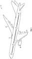
- FIG. 1 illustrates an example of a commercial aircraft 10 having aircraft engines 20 that may embody aspects of the teachings of this disclosure.
- the aircraft 10 includes two wings 22.
- the teachings herein can be applied to any circuit board or controller contained in the aircraft.
- the controller is a FADEC system.
- a FADEC system can be located in a high-temperature environment such as a jet engine, wherein there is a greater amount of heat generated outside the housing of the controller than inside.
- insulation and the use of conventional cooling techniques are typically constrained by specification.
- the PCB can be located in a region in or near and aircraft jet engine 20 as illustrated in FIG.2 .
- FIG. 2 illustrates the electrical chassis 1 as part of an aircraft jet engine 100.
- the different sections of the engine are illustrated, including a compression section 130, a combustion section 140, and an expansion section 150.
- the temperatures of the engine are most extreme in the combustion section 140 and the expansion section 150.
- the electrical chassis 1 is located adjacent to the combustion section 140. This location allows the electrical system for the engine 100 to be assembled with minimal cabling and wire harnesses.
- the location of the electrical chassis 1 as shown is proximal to devices that may require control, such as fuel injector 142. Other locations may be more or less appropriate for a given configuration.
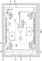
- FIG. 3 shows a PCB 300 located within a chassis 1.
- the PCB includes a substrate 301 on which one or more circuits 306, 308 are disposed.
- the circuits 306, 308 can be for example, processors, memory devices, transmitters, etc. While two circuits 306, 308 are shown, the skilled artisan will realize that this is but one example and any number of circuits can be located on the PCB 300.
- the PCB 300 can be formed of typical materials in one embodiment. Such materials can include a non-conductive substrate such as a laminate formed of by curing under pressure and temperature layers of cloth or paper with thermoset resin to form an integral final piece of uniform thickness. There can be one or more laminate layers and circuits (e.g,. 306, 308) can be electrically connected by copper conductive tracks formed on the laminate or between layers of laminate.
- the substrate can be formed such they have high thermal conductivity by using materials such as beryllium oxide or various forms of silica, in order to conduct the heat generated by the electrical circuits 306, 308 away from the system.
- the chassis 1 may be comprised of a lightweight, high strength material, such as a carbon composite.
- the chassis 1 and the PCB 300 may be formed as a unitary structure from the same substance.
- the PCB 300 includes four outer edges, 320, 322, 324, 326.
- the first edge 320 is opposite the third edge 324 and the second edge 322 is opposite the fourth edge 326.
- First and second board stiffeners 302, 304 are disposed along the first and third edges 320, 324.
- the board stiffeners 302, 304 provide structural rigidity for the PCB 300.
- the board stiffeners 302, 304 can be formed of a material that has a first Seebeck coefficient.
- the board stiffeners 302, 304 are formed of a conductive material that is not copper.
- the board stiffeners 302, 304 can be formed of aluminum or steel.
- the board stiffeners 302, 304 are connected to one another by metal traces generally referred to as traces 340 in FIG. 3 .
- traces 340 in FIG. 3 .
- three traces 340a, 340b and 340c are illustrated.
- the number of traces in not as limiting and are shown by way of example.
- the traces 340 can be formed of a material that is different than the first material of the board stiffeners and, as such, have a second Seebeck coefficient that is different than the first Seebeck coefficient.
- the traces 340 are formed of copper. As shown the traces 340 are all on top of the substrate 301. Of course, the traces 340 could be partially or wholly on the bottom of the substrate 301 or between layers of the substrate 301.
- the traces 340 contact the board stiffeners 302, 304 at junctions 351, 352, 353 and 354.
- the stiffener junctions 351, 352, 353 and 354 When one of the stiffener junctions 351, 352, 353 and 354 is exposed to a quick change in temperature, there is a thermal gradient across the stiffener for a short period of time. During this time period, a thermoelectric voltage is created across due to the dissimilar materials of the board stiffeners 302, 304 and the traces 340 that can be sensed with electrical instrumentation. This can be used to detect fire or burst duct conditions impinging on the areas near the stiffener terminations. As shown in FIG. 3 , the temperatures at junctions 351, 352, 353 and 354 are T1, T2, T3 and T4, respectively.
- junction 351 is a first end of the second board stiffener 304
- junction 352 is a second end of the second board stiffener 304
- junction 353 is a first end of the first board stiffener 302
- junction 354 is a second end of the first board stiffener 302.
- the traces 340a/340b are connected to the inputs of a differential amplifier 310.
- a threshold it can be determined if one of the edges is at a higher heat than another edge. If the voltage at the inverting input of the differential amplifier 310 (e.g., the voltage on trace 340b) is greater than the voltage at the non-inverting input of the differential amplifier 310, then the output of the differential amplifier 310 will be negative. If the voltage at the inverting input of the differential amplifier 310 (e.g., the voltage on trace 340b) is less than the voltage at the non-inverting input of the differential amplifier 310, then the output of the differential amplifier 310 will be positive.
- a controller 312 can determine a side of the circuit board exposed to a high temperature based on the output of the differential amplifier 310 in line with the above description.
- a combination of the differential amplifier and the controller 312 is referred to as a control unit 314.
- stiffeners 302, 304 can be connected to a common mode voltage (Vcm).
- Vcm common mode voltage
- Application of Vcm to the inverting and non-inverting inputs of the differential amplifier 310 through stiffeners 302/304 as illustrated can be used to test the continuity of the connections.
- FIG. 4 shows an equivalent circuit of the connections of the traces 340a-340c and the stiffeners 302, 304.
- S stiffeners is the first Seebeck coefficient and S traces is the second Seebeck coefficient.
- Vout will only be different for a short time period due to decay of thermal gradient over time.
- the output of the differential amplifier 310 will typically only produce pulse such as shown by waveform 402.
- the differential amplifier 310 produces a positive pulse when the high temperature is closer to the second end (junction 354) of the first board stiffener 302 or the first end (junction 351) of the second board stiffener 304 and a negative pulse when the high temperature is closer to the second end (junction 352) of second board stiffener 304 or the first end (junction 353) of the first board stiffener 302.
- the teachings herein can be applied to a housing that includes a PCB and that includes elements that allow for determining the side of the chassis that is closer to a high temperature source external to it based on a voltage differential produced as described above as along as the orientation of the PCB in the chassis is known.
Landscapes
- Engineering & Computer Science (AREA)
- Physics & Mathematics (AREA)
- General Physics & Mathematics (AREA)
- Microelectronics & Electronic Packaging (AREA)
- Mechanical Engineering (AREA)
- General Engineering & Computer Science (AREA)
- Structure Of Printed Boards (AREA)
Abstract
Description
- Exemplary embodiments pertain to the art of electronic circuits and, in particular, to determining that an electronic circuit is exposed to a high temperature and a side of the circuit being exposed to that high temperature.
- Thermal management of aircraft mounted electronic components is becoming increasingly more challenging with the higher density of more powerful, but smaller electronic components. Currently, embedded heat sinks have been used to move heat from a hot electronic component on a printed wiring board to cooler locations.
- When a sudden source of intense heat is applied to an electronic component, such as a full authority digital engine control (FADEC) system, circuits in the component closest to the heat source can be exposed to temperatures that are outside of the specified operating range of the circuits. In such a case, it is very likely that more thermally isolated sections of the controller will be operating at normal temperatures.
- As circuit operation may vary depending on temperature, one challenge presented to an electronics designer is to detect changes in temperature which may have a functional impact local to the heat source at one location on a circuit board in the controller but not affect circuits on another part of a circuit board.
- In the context of aircraft, the sources of such heat can be from, for example, a fire or a burst duct.
- Disclosed in embodiment is a system for determining a side of an electrical circuit exposed to a high temperature. The system of this embodiment includes a printed circuit board having at least two outer edges, a first board stiffener disposed along a first of the two outer edges, the first board stiffener having a first end and a second end and a second board stiffener disposed along a second of the two outer edges, the second board stiffener having a first end and a second end, wherein the first and second board stiffeners are formed of a first material having a first Seebeck coefficient. The system also includes a control unit and a plurality of traces formed of a second material that is different than the first material and has a second Seebeck coefficient. The traces connect the first end of the first and second board stiffeners to the control unit and connect the second end of the first and second board stiffeners to one another. The control unit determines whether the first edge or second edge is closer to the high temperature based on a voltage differential between a trace connecting it to the first end of the first board stiffener and a trace connecting to the first end of the second board stiffener.
- In one embodiment, in a system of any prior embodiment, the traces are formed of copper.
- In one embodiment, in a system of any prior embodiment, the first and second traces are formed of a material that is not copper.
- In one embodiment, in a system of any prior embodiment, the control unit includes a differential amplifier.
- In one embodiment, in a system of any prior embodiment, the traces are connected to the differential amplifier.
- In one embodiment, in a system of any prior embodiment, the differential amplifier produces a positive pulse when the high temperature is closer to the first outer edge and negative pulse when the high temperature is closer to the second outer edge.
- In one embodiment, in a system of any prior embodiment, the voltage differential (Vout) is equal defined as:

- In another embodiment, an electronics chassis that includes a printed circuit board having at least two outer edges, a first board stiffener disposed along a first of the two outer edges, the first board stiffener having a first end and a second end and a second board stiffener disposed along a second of the two outer edges, the second board stiffener having a first end and a second end, wherein the first and second board stiffeners are formed of a first material having a first Seebeck coefficient is disclosed. The chassis also includes a control unit and a plurality of traces formed of a second material that is different than the first material and has a second Seebeck coefficient, the traces connecting the first end of the first and second board stiffeners to the control unit and connecting the second end of the first and second board stiffeners to one another. The control unit determines whether the first edge or second edge is closer a high temperature source external to the chassis based on a voltage differential between a trace connecting it to the first end of the first board stiffener and a trace connecting to the first end of the second board stiffener.
- In one embodiment, in a chassis of any prior embodiment, the traces are formed of copper.
- In one embodiment, in a chassis of any prior embodiment, the first and second traces are formed of a material that is not copper.
- In one embodiment, in a chassis of any prior embodiment, the control unit includes a differential amplifier.
- In one embodiment, in a chassis of any prior embodiment, the traces are connected to the differential amplifier.
- In one embodiment, in a chassis of any prior embodiment, the differential amplifier produces a positive pulse when the high temperature is closer to the first outer edge and negative pulse when the high temperature is closer to the second outer edge.
- In one embodiment, in a chassis of any prior embodiment, the housing is formed of the same material as the printed circuit board.
- In one embodiment, in a chassis of any prior embodiment, the voltage differential (Vout) is equal defined as:

- The following descriptions should not be considered limiting in any way. With reference to the accompanying drawings, like elements are numbered alike:
-
FIG. 1 is an aircraft in which embodiments of the present invention may be implemented; -
FIG. 2 is a turbine engine in which embodiments of the present invention may be implemented; -
FIG. 3 is printed circuit board disposed in a chassis according to one embodiment; and -
FIG. 4 is an equivalent circuit to that on the printed circuit board ofFIG. 4 . - A detailed description of one or more embodiments of the disclosed apparatus and method are presented herein by way of exemplification and not limitation with reference to the Figures.
- For reference, in one embodiment, the circuit board temperature sensor of one embodiment can be included in an aircraft.
FIG. 1 illustrates an example of acommercial aircraft 10 havingaircraft engines 20 that may embody aspects of the teachings of this disclosure. Theaircraft 10 includes twowings 22. - The teachings herein can be applied to any circuit board or controller contained in the aircraft. In one embodiment, the controller is a FADEC system. Such a system can be located in a high-temperature environment such as a jet engine, wherein there is a greater amount of heat generated outside the housing of the controller than inside. With respect to jet engines, insulation and the use of conventional cooling techniques are typically constrained by specification. Thus, in order to maintain an adequate operating temperature for the electrical components, it is often necessary to determine if circuits on one side of a printed circuit board (PCB) in the controller are experiencing greater heat than those on another side. While not limiting, to illustrate one environment where the teachings herein can be applied, the PCB can be located in a region in or near and
aircraft jet engine 20 as illustrated inFIG.2 . - In
FIG 2 , a PCB can be contained in an electrical chassis 1.FIG. 2 illustrates the electrical chassis 1 as part of an aircraft jet engine 100. In the illustrated embodiment, the different sections of the engine are illustrated, including acompression section 130, acombustion section 140, and anexpansion section 150. The temperatures of the engine are most extreme in thecombustion section 140 and theexpansion section 150. In this example, the electrical chassis 1 is located adjacent to thecombustion section 140. This location allows the electrical system for the engine 100 to be assembled with minimal cabling and wire harnesses. For example, the location of the electrical chassis 1 as shown is proximal to devices that may require control, such asfuel injector 142. Other locations may be more or less appropriate for a given configuration. -
FIG. 3 shows a PCB 300 located within a chassis 1. The PCB includes asubstrate 301 on which one ormore circuits circuits circuits PCB 300. The PCB 300 can be formed of typical materials in one embodiment. Such materials can include a non-conductive substrate such as a laminate formed of by curing under pressure and temperature layers of cloth or paper with thermoset resin to form an integral final piece of uniform thickness. There can be one or more laminate layers and circuits (e.g,. 306, 308) can be electrically connected by copper conductive tracks formed on the laminate or between layers of laminate. - In one embodiment, the substrate can be formed such they have high thermal conductivity by using materials such as beryllium oxide or various forms of silica, in order to conduct the heat generated by the
electrical circuits - The chassis 1 may be comprised of a lightweight, high strength material, such as a carbon composite. In other examples, the chassis 1 and the
PCB 300 may be formed as a unitary structure from the same substance. - As shown, the
PCB 300 includes four outer edges, 320, 322, 324, 326. Thefirst edge 320 is opposite thethird edge 324 and thesecond edge 322 is opposite thefourth edge 326. - First and
second board stiffeners third edges board stiffeners PCB 300. Theboard stiffeners board stiffeners board stiffeners - The
board stiffeners FIG. 3 . In particular, threetraces substrate 301. Of course, the traces 340 could be partially or wholly on the bottom of thesubstrate 301 or between layers of thesubstrate 301. - As shown, the traces 340 contact the
board stiffeners junctions stiffener junctions board stiffeners FIG. 3 , the temperatures atjunctions junction 351 is a first end of thesecond board stiffener 304,junction 352 is a second end of thesecond board stiffener 304,junction 353 is a first end of thefirst board stiffener 302, andjunction 354 is a second end of thefirst board stiffener 302. - The
traces 340a/340b are connected to the inputs of adifferential amplifier 310. When the difference between the voltages on thetraces 340a/340b exceeds a threshold, it can be determined if one of the edges is at a higher heat than another edge. If the voltage at the inverting input of the differential amplifier 310 (e.g., the voltage ontrace 340b) is greater than the voltage at the non-inverting input of thedifferential amplifier 310, then the output of thedifferential amplifier 310 will be negative. If the voltage at the inverting input of the differential amplifier 310 (e.g., the voltage ontrace 340b) is less than the voltage at the non-inverting input of thedifferential amplifier 310, then the output of thedifferential amplifier 310 will be positive. Acontroller 312 can determine a side of the circuit board exposed to a high temperature based on the output of thedifferential amplifier 310 in line with the above description. Herein, a combination of the differential amplifier and thecontroller 312 is referred to as acontrol unit 314. - In addition, the
stiffeners differential amplifier 310 throughstiffeners 302/304 as illustrated can be used to test the continuity of the connections. - For simplicity,
FIG. 4 shows an equivalent circuit of the connections of thetraces 340a-340c and thestiffeners differential amplifier 310 can be expressed as:
- Vout will only be different for a short time period due to decay of thermal gradient over time. Thus, the output of the
differential amplifier 310 will typically only produce pulse such as shown bywaveform 402. - In one embodiment, the
differential amplifier 310 produces a positive pulse when the high temperature is closer to the second end (junction 354) of thefirst board stiffener 302 or the first end (junction 351) of thesecond board stiffener 304 and a negative pulse when the high temperature is closer to the second end (junction 352) ofsecond board stiffener 304 or the first end (junction 353) of thefirst board stiffener 302. - Given that the PCB is in chassis 1, the skilled artisan will realize that the teachings herein can be applied to a housing that includes a PCB and that includes elements that allow for determining the side of the chassis that is closer to a high temperature source external to it based on a voltage differential produced as described above as along as the orientation of the PCB in the chassis is known.
- The term "about" is intended to include the degree of error associated with measurement of the particular quantity based upon the equipment available at the time of filing the application.
- The terminology used herein is for the purpose of describing particular embodiments only and is not intended to be limiting of the present disclosure. As used herein, the singular forms "a", "an" and "the" are intended to include the plural forms as well, unless the context clearly indicates otherwise. It will be further understood that the terms "comprises" and/or "comprising," when used in this specification, specify the presence of stated features, integers, steps, operations, elements, and/or components, but do not preclude the presence or addition of one or more other features, integers, steps, operations, element components, and/or groups thereof.
- While the present disclosure has been described with reference to an exemplary embodiment or embodiments, it will be understood by those skilled in the art that various changes may be made and equivalents may be substituted for elements thereof without departing from the scope of the invention as defined by the claims. In addition, many modifications may be made to adapt a particular situation or material to the teachings of the present disclosure without departing from the scope of the invention. Therefore, it is intended that the present disclosure not be limited to the particular embodiment disclosed as the best mode contemplated for carrying out this present disclosure, but that the present disclosure will include all embodiments falling within the scope of the claims.
Claims (15)
- A system for determining a side of an electrical circuit exposed to a high temperature, the system including:a printed circuit board (300) having at least two outer edges (320,322,324,326);a first board stiffener (302) disposed along a first of the two outer edges, the first board stiffener having a first end and a second end;a second board stiffener (304) disposed along a second of the two outer edges, the second board stiffener having a first end and a second end, wherein the first and second board stiffeners are formed of a first material having a first Seebeck coefficient;a control unit (312);a plurality of traces (340) formed of a second material that is different than the first material and has a second Seebeck coefficient, the traces connecting the first end of the first and second board stiffeners to the control unit and connecting the second end of the first and second board stiffeners to one another;wherein the control unit determines whether the first edge or second edge is closer to the high temperature based on a voltage differential between a trace connecting it to the first end of the first board stiffener and a trace connecting to the first end of the second board stiffener.
- The system of claim 1, wherein the traces are formed of copper.
- The system of claim 1, wherein the first and second traces are formed of a material that is not copper.
- The system of claim 1, 2 or 3, wherein the control unit includes a differential amplifier (310).
- The system of claim 4, wherein the traces are connected to the differential amplifier.
- The system of claim 5, wherein the differential amplifier (310) produces a positive pulse when the high temperature is closer to the second end of the first board stiffener or the first end of the second board stiffener and a negative pulse when the high temperature is closer to the second end of second board stiffener or the first end of the first board stiffener.
- The system of any preceding claim, wherein the voltage differential (Vout) is defined as:

- An electronics chassis comprising:a printed circuit board (300) having at least two outer edges;a first board stiffener (302) disposed along a first of the two outer edges, the first board stiffener having a first end and a second end;a second board stiffener (304) disposed along a second of the two outer edges, the second board stiffener having a first end and a second end, wherein the first and second board stiffeners are formed of a first material having a first Seebeck coefficient;a control unit (312);a plurality of traces (340) formed of a second material that is different than the first material and has a second Seebeck coefficient, the traces connecting the first end of the first and second board stiffeners to the control unit and connecting the second end of the first and second board stiffeners to one another;wherein the control unit determines whether the first edge or second edge is closer a high temperature source external to the chassis based on a voltage differential between a trace connecting it to the first end of the first board stiffener and a trace connecting to the first end of the second board stiffener.
- The chassis of claim 8, wherein the traces are formed of copper.
- The chassis of claim 8, wherein the first and second traces are formed of a material that is not copper.
- The chassis of claim 8, 9 or 10, wherein the control unit includes a differential amplifier (310).
- The chassis of claim 11, wherein the traces are connected to the differential amplifier.
- The chassis of claim 12, wherein the differential amplifier produces a positive pulse when the high temperature is closer to the second end of the first board stiffener or the first end of the second board stiffener and a negative pulse when the high temperature is closer to the second end of second board stiffener or the first end of the first board stiffener.
- The chassis of any of claims 8 to 13, wherein housing is the formed of a different material than the printed circuit board.
- The chassis of any of claims 8 to 14, wherein the voltage differential (Vout) is defined as:

Applications Claiming Priority (1)
| Application Number | Priority Date | Filing Date | Title |
|---|---|---|---|
| US16/121,823 US10962422B2 (en) | 2018-09-05 | 2018-09-05 | Differential and high rate of change temperature sensing circuit |
Publications (2)
| Publication Number | Publication Date |
|---|---|
| EP3620766A1 true EP3620766A1 (en) | 2020-03-11 |
| EP3620766B1 EP3620766B1 (en) | 2021-06-16 |
Family
ID=67777235
Family Applications (1)
| Application Number | Title | Priority Date | Filing Date |
|---|---|---|---|
| EP19194144.2A Active EP3620766B1 (en) | 2018-09-05 | 2019-08-28 | Differential and high rate of change temperature sensing circuit |
Country Status (2)
| Country | Link |
|---|---|
| US (1) | US10962422B2 (en) |
| EP (1) | EP3620766B1 (en) |
Families Citing this family (1)
| Publication number | Priority date | Publication date | Assignee | Title |
|---|---|---|---|---|
| CN117082722B (en) * | 2023-09-19 | 2025-08-22 | 荣耀终端股份有限公司 | PCB, PCB temperature measurement circuits and electronic equipment |
Citations (3)
| Publication number | Priority date | Publication date | Assignee | Title |
|---|---|---|---|---|
| US6472612B2 (en) * | 2001-03-30 | 2002-10-29 | Intel Corporation | Printed circuit board with embedded thermocouple junctions |
| KR100671485B1 (en) * | 2005-04-19 | 2007-01-19 | 주식회사 씨너텍 | Thermostat of probe card for wafer burn-in test |
| US20140326715A1 (en) * | 2013-05-03 | 2014-11-06 | Rolls-Royce Plc | Composite structure |
Family Cites Families (17)
| Publication number | Priority date | Publication date | Assignee | Title |
|---|---|---|---|---|
| US5607538A (en) * | 1995-09-07 | 1997-03-04 | Ford Motor Company | Method of manufacturing a circuit assembly |
| US6039471A (en) * | 1996-05-22 | 2000-03-21 | Integrated Device Technology, Inc. | Device for simulating dissipation of thermal power by a board supporting an electronic component |
| JP2001282396A (en) * | 2000-03-24 | 2001-10-12 | Internatl Business Mach Corp <Ibm> | Power generating mechanism and computer device and electronic equipment |
| US7032119B2 (en) * | 2000-09-27 | 2006-04-18 | Amphus, Inc. | Dynamic power and workload management for multi-server system |
| USRE40866E1 (en) * | 2000-09-27 | 2009-08-04 | Huron Ip Llc | System, method, and architecture for dynamic server power management and dynamic workload management for multiserver environment |
| US20040174674A1 (en) | 2003-03-04 | 2004-09-09 | Stewart Thomas E. | Method for monitoring a computer system |
| US7733224B2 (en) * | 2006-06-30 | 2010-06-08 | Bao Tran | Mesh network personal emergency response appliance |
| CA2877959C (en) | 2006-08-22 | 2017-06-13 | Charles F. Barry | Apparatus and method for thermal stabilization of pcb-mounted electronic components within an enclosed housing |
| DE112008003664T5 (en) * | 2008-01-31 | 2010-12-30 | Hewlett-Packard Development Co., L.P., Houston | Insulating opening in circuit boards |
| US20090211603A1 (en) * | 2008-02-22 | 2009-08-27 | Tokyo Electron Limited | System and Method For Removing Post-Etch Residue |
| CN102112181B (en) | 2008-07-03 | 2012-11-28 | 法克有限公司 | Flame detection and suppression system using a thermoelectric generator |
| US8602643B2 (en) | 2010-07-06 | 2013-12-10 | David Phillip Gardiner | Method and apparatus for measurement of temperature and rate of change of temperature |
| US9426932B2 (en) * | 2013-03-13 | 2016-08-23 | Silicon Graphics International Corp. | Server with heat pipe cooling |
| US9433074B2 (en) | 2013-04-29 | 2016-08-30 | Toyota Motor Engineering & Manufacturing North America, Inc. | Printed wiring boards having thermal management features and thermal management apparatuses comprising the same |
| WO2016073944A1 (en) * | 2014-11-06 | 2016-05-12 | The Regents Of The University Of California | Autonomous thermoelectric energy harvesting platform for biomedical sensors |
| DE102015207857A1 (en) | 2015-04-29 | 2016-11-03 | Robert Bosch Gmbh | Thermoelectric device and manufacturing method thereof |
| US9661745B1 (en) * | 2015-12-22 | 2017-05-23 | Intel Corporation | Vacuum lamination of depth-sensing camera module PCB to stiffener using built-in vacuum channels |
-
2018
- 2018-09-05 US US16/121,823 patent/US10962422B2/en active Active
-
2019
- 2019-08-28 EP EP19194144.2A patent/EP3620766B1/en active Active
Patent Citations (3)
| Publication number | Priority date | Publication date | Assignee | Title |
|---|---|---|---|---|
| US6472612B2 (en) * | 2001-03-30 | 2002-10-29 | Intel Corporation | Printed circuit board with embedded thermocouple junctions |
| KR100671485B1 (en) * | 2005-04-19 | 2007-01-19 | 주식회사 씨너텍 | Thermostat of probe card for wafer burn-in test |
| US20140326715A1 (en) * | 2013-05-03 | 2014-11-06 | Rolls-Royce Plc | Composite structure |
Also Published As
| Publication number | Publication date |
|---|---|
| EP3620766B1 (en) | 2021-06-16 |
| US20200072678A1 (en) | 2020-03-05 |
| US10962422B2 (en) | 2021-03-30 |
Similar Documents
| Publication | Publication Date | Title |
|---|---|---|
| US8596113B2 (en) | Intake air temperature sensor and thermal airflow meter including the same | |
| EP1887366B1 (en) | Method and system for measurement of current flows in fastener arrays | |
| US20110106475A1 (en) | Total Air Temperature Probe and Method for Reducing De-Icing/Anti-Icing Heater Error | |
| US8757874B2 (en) | Temperature sensing system and method | |
| US10309735B2 (en) | Airflow sensor for a heat sink | |
| EP3840070B1 (en) | Printed circuit board assembly embedded thermal management system using thin-film thermoelectric coolers | |
| EP3620766B1 (en) | Differential and high rate of change temperature sensing circuit | |
| US20140050248A1 (en) | I/o connector incorporating a cold junction | |
| Medvedev et al. | Testing of hidden defects in interconnections | |
| US6881595B2 (en) | Method of and apparatus for testing the quality of printed circuits | |
| US11346725B2 (en) | Temperature measurement | |
| CN213579821U (en) | Thermocouple and electronic equipment | |
| US11609125B2 (en) | Systems and methods for thermal monitoring | |
| US10429248B2 (en) | Temperature sensor | |
| US10477669B2 (en) | Circuit substrate | |
| US11047744B2 (en) | Optimized thermocouple system and method | |
| El Kraye Ziade | Design and implementation of an electronic system for a microgravity experiment | |
| US12078552B2 (en) | Optimized thermocouple system and method | |
| Jahn et al. | Thermal Detection of Degradation in Solder Joints of Passive Components | |
| US10921196B2 (en) | Optimized thermocouple system and method | |
| Lira et al. | Thermal analysis and testing of missile avionics systems | |
| US11125630B2 (en) | Thermometric measurement by meshing of probes, particularly in turbine engines | |
| Jaiswal et al. | Design and Validation of EMI/EMC-Compliant Analog Sensor PCB | |
| Hauter | Equipment Reliability Real and Perceived | |
| Jouppi et al. | Current-carrying capacity of PWB internal conductors in space environments |
Legal Events
| Date | Code | Title | Description |
|---|---|---|---|
| PUAI | Public reference made under article 153(3) epc to a published international application that has entered the european phase |
Free format text: ORIGINAL CODE: 0009012 |
|
| STAA | Information on the status of an ep patent application or granted ep patent |
Free format text: STATUS: THE APPLICATION HAS BEEN PUBLISHED |
|
| AK | Designated contracting states |
Kind code of ref document: A1 Designated state(s): AL AT BE BG CH CY CZ DE DK EE ES FI FR GB GR HR HU IE IS IT LI LT LU LV MC MK MT NL NO PL PT RO RS SE SI SK SM TR |
|
| AX | Request for extension of the european patent |
Extension state: BA ME |
|
| STAA | Information on the status of an ep patent application or granted ep patent |
Free format text: STATUS: REQUEST FOR EXAMINATION WAS MADE |
|
| 17P | Request for examination filed |
Effective date: 20200911 |
|
| RBV | Designated contracting states (corrected) |
Designated state(s): AL AT BE BG CH CY CZ DE DK EE ES FI FR GB GR HR HU IE IS IT LI LT LU LV MC MK MT NL NO PL PT RO RS SE SI SK SM TR |
|
| GRAP | Despatch of communication of intention to grant a patent |
Free format text: ORIGINAL CODE: EPIDOSNIGR1 |
|
| STAA | Information on the status of an ep patent application or granted ep patent |
Free format text: STATUS: GRANT OF PATENT IS INTENDED |
|
| INTG | Intention to grant announced |
Effective date: 20210115 |
|
| GRAS | Grant fee paid |
Free format text: ORIGINAL CODE: EPIDOSNIGR3 |
|
| GRAA | (expected) grant |
Free format text: ORIGINAL CODE: 0009210 |
|
| STAA | Information on the status of an ep patent application or granted ep patent |
Free format text: STATUS: THE PATENT HAS BEEN GRANTED |
|
| AK | Designated contracting states |
Kind code of ref document: B1 Designated state(s): AL AT BE BG CH CY CZ DE DK EE ES FI FR GB GR HR HU IE IS IT LI LT LU LV MC MK MT NL NO PL PT RO RS SE SI SK SM TR |
|
| REG | Reference to a national code |
Ref country code: GB Ref legal event code: FG4D |
|
| REG | Reference to a national code |
Ref country code: CH Ref legal event code: EP |
|
| REG | Reference to a national code |
Ref country code: DE Ref legal event code: R096 Ref document number: 602019005371 Country of ref document: DE |
|
| REG | Reference to a national code |
Ref country code: AT Ref legal event code: REF Ref document number: 1402723 Country of ref document: AT Kind code of ref document: T Effective date: 20210715 |
|
| REG | Reference to a national code |
Ref country code: IE Ref legal event code: FG4D |
|
| REG | Reference to a national code |
Ref country code: LT Ref legal event code: MG9D |
|
| PG25 | Lapsed in a contracting state [announced via postgrant information from national office to epo] |
Ref country code: BG Free format text: LAPSE BECAUSE OF FAILURE TO SUBMIT A TRANSLATION OF THE DESCRIPTION OR TO PAY THE FEE WITHIN THE PRESCRIBED TIME-LIMIT Effective date: 20210916 Ref country code: LT Free format text: LAPSE BECAUSE OF FAILURE TO SUBMIT A TRANSLATION OF THE DESCRIPTION OR TO PAY THE FEE WITHIN THE PRESCRIBED TIME-LIMIT Effective date: 20210616 Ref country code: HR Free format text: LAPSE BECAUSE OF FAILURE TO SUBMIT A TRANSLATION OF THE DESCRIPTION OR TO PAY THE FEE WITHIN THE PRESCRIBED TIME-LIMIT Effective date: 20210616 Ref country code: FI Free format text: LAPSE BECAUSE OF FAILURE TO SUBMIT A TRANSLATION OF THE DESCRIPTION OR TO PAY THE FEE WITHIN THE PRESCRIBED TIME-LIMIT Effective date: 20210616 |
|
| REG | Reference to a national code |
Ref country code: AT Ref legal event code: MK05 Ref document number: 1402723 Country of ref document: AT Kind code of ref document: T Effective date: 20210616 |
|
| REG | Reference to a national code |
Ref country code: NL Ref legal event code: MP Effective date: 20210616 |
|
| PG25 | Lapsed in a contracting state [announced via postgrant information from national office to epo] |
Ref country code: RS Free format text: LAPSE BECAUSE OF FAILURE TO SUBMIT A TRANSLATION OF THE DESCRIPTION OR TO PAY THE FEE WITHIN THE PRESCRIBED TIME-LIMIT Effective date: 20210616 Ref country code: SE Free format text: LAPSE BECAUSE OF FAILURE TO SUBMIT A TRANSLATION OF THE DESCRIPTION OR TO PAY THE FEE WITHIN THE PRESCRIBED TIME-LIMIT Effective date: 20210616 Ref country code: LV Free format text: LAPSE BECAUSE OF FAILURE TO SUBMIT A TRANSLATION OF THE DESCRIPTION OR TO PAY THE FEE WITHIN THE PRESCRIBED TIME-LIMIT Effective date: 20210616 Ref country code: NO Free format text: LAPSE BECAUSE OF FAILURE TO SUBMIT A TRANSLATION OF THE DESCRIPTION OR TO PAY THE FEE WITHIN THE PRESCRIBED TIME-LIMIT Effective date: 20210916 Ref country code: GR Free format text: LAPSE BECAUSE OF FAILURE TO SUBMIT A TRANSLATION OF THE DESCRIPTION OR TO PAY THE FEE WITHIN THE PRESCRIBED TIME-LIMIT Effective date: 20210917 |
|
| PG25 | Lapsed in a contracting state [announced via postgrant information from national office to epo] |
Ref country code: AT Free format text: LAPSE BECAUSE OF FAILURE TO SUBMIT A TRANSLATION OF THE DESCRIPTION OR TO PAY THE FEE WITHIN THE PRESCRIBED TIME-LIMIT Effective date: 20210616 Ref country code: CZ Free format text: LAPSE BECAUSE OF FAILURE TO SUBMIT A TRANSLATION OF THE DESCRIPTION OR TO PAY THE FEE WITHIN THE PRESCRIBED TIME-LIMIT Effective date: 20210616 Ref country code: PT Free format text: LAPSE BECAUSE OF FAILURE TO SUBMIT A TRANSLATION OF THE DESCRIPTION OR TO PAY THE FEE WITHIN THE PRESCRIBED TIME-LIMIT Effective date: 20211018 Ref country code: NL Free format text: LAPSE BECAUSE OF FAILURE TO SUBMIT A TRANSLATION OF THE DESCRIPTION OR TO PAY THE FEE WITHIN THE PRESCRIBED TIME-LIMIT Effective date: 20210616 Ref country code: RO Free format text: LAPSE BECAUSE OF FAILURE TO SUBMIT A TRANSLATION OF THE DESCRIPTION OR TO PAY THE FEE WITHIN THE PRESCRIBED TIME-LIMIT Effective date: 20210616 Ref country code: SM Free format text: LAPSE BECAUSE OF FAILURE TO SUBMIT A TRANSLATION OF THE DESCRIPTION OR TO PAY THE FEE WITHIN THE PRESCRIBED TIME-LIMIT Effective date: 20210616 Ref country code: SK Free format text: LAPSE BECAUSE OF FAILURE TO SUBMIT A TRANSLATION OF THE DESCRIPTION OR TO PAY THE FEE WITHIN THE PRESCRIBED TIME-LIMIT Effective date: 20210616 Ref country code: ES Free format text: LAPSE BECAUSE OF FAILURE TO SUBMIT A TRANSLATION OF THE DESCRIPTION OR TO PAY THE FEE WITHIN THE PRESCRIBED TIME-LIMIT Effective date: 20210616 Ref country code: EE Free format text: LAPSE BECAUSE OF FAILURE TO SUBMIT A TRANSLATION OF THE DESCRIPTION OR TO PAY THE FEE WITHIN THE PRESCRIBED TIME-LIMIT Effective date: 20210616 |
|
| PG25 | Lapsed in a contracting state [announced via postgrant information from national office to epo] |
Ref country code: PL Free format text: LAPSE BECAUSE OF FAILURE TO SUBMIT A TRANSLATION OF THE DESCRIPTION OR TO PAY THE FEE WITHIN THE PRESCRIBED TIME-LIMIT Effective date: 20210616 |
|
| REG | Reference to a national code |
Ref country code: DE Ref legal event code: R097 Ref document number: 602019005371 Country of ref document: DE |
|
| PG25 | Lapsed in a contracting state [announced via postgrant information from national office to epo] |
Ref country code: MC Free format text: LAPSE BECAUSE OF FAILURE TO SUBMIT A TRANSLATION OF THE DESCRIPTION OR TO PAY THE FEE WITHIN THE PRESCRIBED TIME-LIMIT Effective date: 20210616 |
|
| PLBE | No opposition filed within time limit |
Free format text: ORIGINAL CODE: 0009261 |
|
| REG | Reference to a national code |
Ref country code: BE Ref legal event code: MM Effective date: 20210831 |
|
| STAA | Information on the status of an ep patent application or granted ep patent |
Free format text: STATUS: NO OPPOSITION FILED WITHIN TIME LIMIT |
|
| PG25 | Lapsed in a contracting state [announced via postgrant information from national office to epo] |
Ref country code: DK Free format text: LAPSE BECAUSE OF FAILURE TO SUBMIT A TRANSLATION OF THE DESCRIPTION OR TO PAY THE FEE WITHIN THE PRESCRIBED TIME-LIMIT Effective date: 20210616 |
|
| 26N | No opposition filed |
Effective date: 20220317 |
|
| PG25 | Lapsed in a contracting state [announced via postgrant information from national office to epo] |
Ref country code: LU Free format text: LAPSE BECAUSE OF NON-PAYMENT OF DUE FEES Effective date: 20210828 Ref country code: AL Free format text: LAPSE BECAUSE OF FAILURE TO SUBMIT A TRANSLATION OF THE DESCRIPTION OR TO PAY THE FEE WITHIN THE PRESCRIBED TIME-LIMIT Effective date: 20210616 |
|
| PG25 | Lapsed in a contracting state [announced via postgrant information from national office to epo] |
Ref country code: IT Free format text: LAPSE BECAUSE OF FAILURE TO SUBMIT A TRANSLATION OF THE DESCRIPTION OR TO PAY THE FEE WITHIN THE PRESCRIBED TIME-LIMIT Effective date: 20210616 Ref country code: IE Free format text: LAPSE BECAUSE OF NON-PAYMENT OF DUE FEES Effective date: 20210828 Ref country code: BE Free format text: LAPSE BECAUSE OF NON-PAYMENT OF DUE FEES Effective date: 20210831 |
|
| REG | Reference to a national code |
Ref country code: CH Ref legal event code: PL |
|
| PG25 | Lapsed in a contracting state [announced via postgrant information from national office to epo] |
Ref country code: LI Free format text: LAPSE BECAUSE OF NON-PAYMENT OF DUE FEES Effective date: 20220831 Ref country code: CH Free format text: LAPSE BECAUSE OF NON-PAYMENT OF DUE FEES Effective date: 20220831 |
|
| P01 | Opt-out of the competence of the unified patent court (upc) registered |
Effective date: 20230522 |
|
| PG25 | Lapsed in a contracting state [announced via postgrant information from national office to epo] |
Ref country code: CY Free format text: LAPSE BECAUSE OF FAILURE TO SUBMIT A TRANSLATION OF THE DESCRIPTION OR TO PAY THE FEE WITHIN THE PRESCRIBED TIME-LIMIT Effective date: 20210616 |
|
| PG25 | Lapsed in a contracting state [announced via postgrant information from national office to epo] |
Ref country code: HU Free format text: LAPSE BECAUSE OF FAILURE TO SUBMIT A TRANSLATION OF THE DESCRIPTION OR TO PAY THE FEE WITHIN THE PRESCRIBED TIME-LIMIT; INVALID AB INITIO Effective date: 20190828 |
|
| PG25 | Lapsed in a contracting state [announced via postgrant information from national office to epo] |
Ref country code: MK Free format text: LAPSE BECAUSE OF FAILURE TO SUBMIT A TRANSLATION OF THE DESCRIPTION OR TO PAY THE FEE WITHIN THE PRESCRIBED TIME-LIMIT Effective date: 20210616 |
|
| PG25 | Lapsed in a contracting state [announced via postgrant information from national office to epo] |
Ref country code: TR Free format text: LAPSE BECAUSE OF FAILURE TO SUBMIT A TRANSLATION OF THE DESCRIPTION OR TO PAY THE FEE WITHIN THE PRESCRIBED TIME-LIMIT Effective date: 20210616 |
|
| PG25 | Lapsed in a contracting state [announced via postgrant information from national office to epo] |
Ref country code: MT Free format text: LAPSE BECAUSE OF FAILURE TO SUBMIT A TRANSLATION OF THE DESCRIPTION OR TO PAY THE FEE WITHIN THE PRESCRIBED TIME-LIMIT Effective date: 20210616 |
|
| PGFP | Annual fee paid to national office [announced via postgrant information from national office to epo] |
Ref country code: DE Payment date: 20250724 Year of fee payment: 7 |
|
| PGFP | Annual fee paid to national office [announced via postgrant information from national office to epo] |
Ref country code: GB Payment date: 20250724 Year of fee payment: 7 |
|
| PGFP | Annual fee paid to national office [announced via postgrant information from national office to epo] |
Ref country code: FR Payment date: 20250725 Year of fee payment: 7 |