EP3618128A1 - Light reception/emission element module and sensor device - Google Patents
Light reception/emission element module and sensor device Download PDFInfo
- Publication number
- EP3618128A1 EP3618128A1 EP18792230.7A EP18792230A EP3618128A1 EP 3618128 A1 EP3618128 A1 EP 3618128A1 EP 18792230 A EP18792230 A EP 18792230A EP 3618128 A1 EP3618128 A1 EP 3618128A1
- Authority
- EP
- European Patent Office
- Prior art keywords
- light
- light receiving
- receiving element
- reception
- emission element
- Prior art date
- Legal status (The legal status is an assumption and is not a legal conclusion. Google has not performed a legal analysis and makes no representation as to the accuracy of the status listed.)
- Granted
Links
Images





Classifications
-
- H—ELECTRICITY
- H10—SEMICONDUCTOR DEVICES; ELECTRIC SOLID-STATE DEVICES NOT OTHERWISE PROVIDED FOR
- H10F—INORGANIC SEMICONDUCTOR DEVICES SENSITIVE TO INFRARED RADIATION, LIGHT, ELECTROMAGNETIC RADIATION OF SHORTER WAVELENGTH OR CORPUSCULAR RADIATION
- H10F55/00—Radiation-sensitive semiconductor devices covered by groups H10F10/00, H10F19/00 or H10F30/00 being structurally associated with electric light sources and electrically or optically coupled thereto
- H10F55/20—Radiation-sensitive semiconductor devices covered by groups H10F10/00, H10F19/00 or H10F30/00 being structurally associated with electric light sources and electrically or optically coupled thereto wherein the electric light source controls the radiation-sensitive semiconductor devices, e.g. optocouplers
- H10F55/25—Radiation-sensitive semiconductor devices covered by groups H10F10/00, H10F19/00 or H10F30/00 being structurally associated with electric light sources and electrically or optically coupled thereto wherein the electric light source controls the radiation-sensitive semiconductor devices, e.g. optocouplers wherein the radiation-sensitive devices and the electric light source are all semiconductor devices
- H10F55/255—Radiation-sensitive semiconductor devices covered by groups H10F10/00, H10F19/00 or H10F30/00 being structurally associated with electric light sources and electrically or optically coupled thereto wherein the electric light source controls the radiation-sensitive semiconductor devices, e.g. optocouplers wherein the radiation-sensitive devices and the electric light source are all semiconductor devices formed in, or on, a common substrate
-
- H—ELECTRICITY
- H10—SEMICONDUCTOR DEVICES; ELECTRIC SOLID-STATE DEVICES NOT OTHERWISE PROVIDED FOR
- H10F—INORGANIC SEMICONDUCTOR DEVICES SENSITIVE TO INFRARED RADIATION, LIGHT, ELECTROMAGNETIC RADIATION OF SHORTER WAVELENGTH OR CORPUSCULAR RADIATION
- H10F55/00—Radiation-sensitive semiconductor devices covered by groups H10F10/00, H10F19/00 or H10F30/00 being structurally associated with electric light sources and electrically or optically coupled thereto
-
- G—PHYSICS
- G01—MEASURING; TESTING
- G01S—RADIO DIRECTION-FINDING; RADIO NAVIGATION; DETERMINING DISTANCE OR VELOCITY BY USE OF RADIO WAVES; LOCATING OR PRESENCE-DETECTING BY USE OF THE REFLECTION OR RERADIATION OF RADIO WAVES; ANALOGOUS ARRANGEMENTS USING OTHER WAVES
- G01S17/00—Systems using the reflection or reradiation of electromagnetic waves other than radio waves, e.g. lidar systems
- G01S17/02—Systems using the reflection of electromagnetic waves other than radio waves
- G01S17/04—Systems determining the presence of a target
-
- G—PHYSICS
- G01—MEASURING; TESTING
- G01S—RADIO DIRECTION-FINDING; RADIO NAVIGATION; DETERMINING DISTANCE OR VELOCITY BY USE OF RADIO WAVES; LOCATING OR PRESENCE-DETECTING BY USE OF THE REFLECTION OR RERADIATION OF RADIO WAVES; ANALOGOUS ARRANGEMENTS USING OTHER WAVES
- G01S17/00—Systems using the reflection or reradiation of electromagnetic waves other than radio waves, e.g. lidar systems
- G01S17/02—Systems using the reflection of electromagnetic waves other than radio waves
- G01S17/06—Systems determining position data of a target
- G01S17/08—Systems determining position data of a target for measuring distance only
-
- G—PHYSICS
- G01—MEASURING; TESTING
- G01S—RADIO DIRECTION-FINDING; RADIO NAVIGATION; DETERMINING DISTANCE OR VELOCITY BY USE OF RADIO WAVES; LOCATING OR PRESENCE-DETECTING BY USE OF THE REFLECTION OR RERADIATION OF RADIO WAVES; ANALOGOUS ARRANGEMENTS USING OTHER WAVES
- G01S7/00—Details of systems according to groups G01S13/00, G01S15/00, G01S17/00
- G01S7/48—Details of systems according to groups G01S13/00, G01S15/00, G01S17/00 of systems according to group G01S17/00
- G01S7/481—Constructional features, e.g. arrangements of optical elements
- G01S7/4811—Constructional features, e.g. arrangements of optical elements common to transmitter and receiver
- G01S7/4813—Housing arrangements
-
- G—PHYSICS
- G01—MEASURING; TESTING
- G01V—GEOPHYSICS; GRAVITATIONAL MEASUREMENTS; DETECTING MASSES OR OBJECTS; TAGS
- G01V8/00—Prospecting or detecting by optical means
- G01V8/10—Detecting, e.g. by using light barriers
-
- H—ELECTRICITY
- H03—ELECTRONIC CIRCUITRY
- H03K—PULSE TECHNIQUE
- H03K17/00—Electronic switching or gating, i.e. not by contact-making and –breaking
- H03K17/94—Electronic switching or gating, i.e. not by contact-making and –breaking characterised by the way in which the control signals are generated
- H03K17/941—Electronic switching or gating, i.e. not by contact-making and –breaking characterised by the way in which the control signals are generated using an optical detector
-
- H—ELECTRICITY
- H10—SEMICONDUCTOR DEVICES; ELECTRIC SOLID-STATE DEVICES NOT OTHERWISE PROVIDED FOR
- H10F—INORGANIC SEMICONDUCTOR DEVICES SENSITIVE TO INFRARED RADIATION, LIGHT, ELECTROMAGNETIC RADIATION OF SHORTER WAVELENGTH OR CORPUSCULAR RADIATION
- H10F55/00—Radiation-sensitive semiconductor devices covered by groups H10F10/00, H10F19/00 or H10F30/00 being structurally associated with electric light sources and electrically or optically coupled thereto
- H10F55/10—Radiation-sensitive semiconductor devices covered by groups H10F10/00, H10F19/00 or H10F30/00 being structurally associated with electric light sources and electrically or optically coupled thereto wherein the radiation-sensitive semiconductor devices control the electric light source, e.g. image converters, image amplifiers or image storage devices
- H10F55/15—Radiation-sensitive semiconductor devices covered by groups H10F10/00, H10F19/00 or H10F30/00 being structurally associated with electric light sources and electrically or optically coupled thereto wherein the radiation-sensitive semiconductor devices control the electric light source, e.g. image converters, image amplifiers or image storage devices wherein the radiation-sensitive devices and the electric light source are all semiconductor devices
- H10F55/155—Radiation-sensitive semiconductor devices covered by groups H10F10/00, H10F19/00 or H10F30/00 being structurally associated with electric light sources and electrically or optically coupled thereto wherein the radiation-sensitive semiconductor devices control the electric light source, e.g. image converters, image amplifiers or image storage devices wherein the radiation-sensitive devices and the electric light source are all semiconductor devices formed in, or on, a common substrate
-
- H—ELECTRICITY
- H10—SEMICONDUCTOR DEVICES; ELECTRIC SOLID-STATE DEVICES NOT OTHERWISE PROVIDED FOR
- H10F—INORGANIC SEMICONDUCTOR DEVICES SENSITIVE TO INFRARED RADIATION, LIGHT, ELECTROMAGNETIC RADIATION OF SHORTER WAVELENGTH OR CORPUSCULAR RADIATION
- H10F77/00—Constructional details of devices covered by this subclass
- H10F77/20—Electrodes
- H10F77/206—Electrodes for devices having potential barriers
-
- H—ELECTRICITY
- H10—SEMICONDUCTOR DEVICES; ELECTRIC SOLID-STATE DEVICES NOT OTHERWISE PROVIDED FOR
- H10F—INORGANIC SEMICONDUCTOR DEVICES SENSITIVE TO INFRARED RADIATION, LIGHT, ELECTROMAGNETIC RADIATION OF SHORTER WAVELENGTH OR CORPUSCULAR RADIATION
- H10F77/00—Constructional details of devices covered by this subclass
- H10F77/30—Coatings
- H10F77/306—Coatings for devices having potential barriers
- H10F77/331—Coatings for devices having potential barriers for filtering or shielding light, e.g. multicolour filters for photodetectors
- H10F77/334—Coatings for devices having potential barriers for filtering or shielding light, e.g. multicolour filters for photodetectors for shielding light, e.g. light blocking layers or cold shields for infrared detectors
-
- H—ELECTRICITY
- H03—ELECTRONIC CIRCUITRY
- H03K—PULSE TECHNIQUE
- H03K2217/00—Indexing scheme related to electronic switching or gating, i.e. not by contact-making or -breaking covered by H03K17/00
- H03K2217/94—Indexing scheme related to electronic switching or gating, i.e. not by contact-making or -breaking covered by H03K17/00 characterised by the way in which the control signal is generated
- H03K2217/941—Indexing scheme related to electronic switching or gating, i.e. not by contact-making or -breaking covered by H03K17/00 characterised by the way in which the control signal is generated using an optical detector
- H03K2217/94102—Indexing scheme related to electronic switching or gating, i.e. not by contact-making or -breaking covered by H03K17/00 characterised by the way in which the control signal is generated using an optical detector characterised by the type of activation
- H03K2217/94108—Indexing scheme related to electronic switching or gating, i.e. not by contact-making or -breaking covered by H03K17/00 characterised by the way in which the control signal is generated using an optical detector characterised by the type of activation making use of reflection
Definitions
- the present disclosure relates to a light reception/emission element module and a sensor device.
- Patent Literature 1 a reflection type optical coupling device in which a light emitting portion and a light receiving portion are mounted on a substrate is disclosed (see, for example, Patent Literature 1).
- Patent Literature 1 Japanese Unexamined Patent Publication JP-A 5-152603(1993)
- a light reception/emission element module it is required to monitor the intensity of light emission in a light emitting portion.
- the light reception/emission element module of the disclosure comprises a substrate, a light emitting element that is disposed on the substrate, a first light receiving element that is disposed on the substrate apart from the light emitting element, and an upper wall that is located above the substrate.
- the upper wall comprises a facing surface facing the light emitting element and the first light receiving element.
- the intensity of light emission in a light emitting portion can be monitored.
- a first direction D1 described in the following description is a direction along an X axis
- a second direction D2 is a direction along a Y axis.
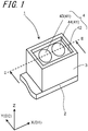
- FIGS. 1 and 2 schematically show an example of a light reception/emission element module of the disclosure.
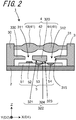
- FIG. 2 is a cross-sectional view of the light reception/emission element module shown in FIG. 1 taken along the line II-II.
- a light reception/emission element module 1 can sense an object, for example, by irradiating the object with light from a light emitting portion and detecting reflected light from the object with a light receiving portion.
- the light reception/emission element module 1 can be incorporated into an image forming apparatus such as a copier or a printer, for example, to detect position information, distance information, density information, and the like of an object such as toner or media.
- the light reception/emission element module 1 comprises a wiring substrate 2, a housing 3 disposed on the wiring substrate 2, and a lens member 4 disposed on the housing 3. Further, as shown in FIG. 2 , in the housing 3, a light reception/emission element 5 mounted on the wiring substrate 2 is disposed.
- the wiring substrate 2 can support the light reception/emission element 5.
- the wiring substrate 2 can be electrically connected to an external device to drive the light reception/emission element 5.
- the light reception/emission element 5 may be mounted on the wiring substrate 2 and electrically connected by a bonding wire.
- the wiring substrate 2 may be formed, for example, in a rectangular shape.
- the wiring substrate 2 can be formed, for example, by laminating an insulating layer and a wiring.
- the wiring substrate 2 may be, for example, a resin substrate or a ceramic substrate.
- the wiring substrate 2 of the disclosure is a resin substrate.
- the insulating layer of the resin substrate is a resin layer, and the insulating layer of the ceramic substrate is a ceramic layer.
- the light reception/emission element 5 can emit light and detect incident light.
- the light reception/emission element 5 comprises a substrate 51, and a light emitting element 52, a light receiving element 54, and a plurality of electrodes 55 which are disposed on the substrate 51.
- the light reception/emission element 5 comprises a first light receiving element 53 in addition to the light receiving element 54 (second light receiving element 54) in order to monitor the light emission intensity of the light emitting element 52.
- the light emitting element 52 and the second light receiving element 54 are aligned along the first direction D1.
- the first light receiving element 53 is disposed in the region between the light emitting element 52 and the second light receiving element 54.
- the substrate 51 can support the light emitting element 52, and the first light receiving element 53 and the second light receiving element 54.
- the substrate 51 may be made of, for example, a semiconductor material.
- the substrate 51 may be, for example, a substrate of silicon (Si) crystal.
- the substrate 51 may have, for example, a plate shape.
- the thickness of the substrate 51 may be, for example, 300 ⁇ m or more and 400 ⁇ m or less.
- the planar shape of the substrate 51 may be, for example, a rectangular shape.
- the substrate 51 can be formed, for example, by slicing an ingot of silicon (Si) into a wafer.
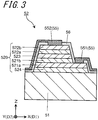
- FIG. 3 is an enlarged view of the light emitting element 52 in the cross section of FIG. 2 .
- the light emitting element 52 can emit light when a voltage is applied.
- the light emitting element 52 may be, for example, a light emitting diode (LED) or a laser diode (LD).
- the light emitting element 52 includes a plurality of semiconductor layers 520 disposed on an upper surface of the substrate 51, and a first electrode 551 and a second electrode 552 for applying a voltage to the plurality of semiconductor layers 520.
- the plurality of semiconductor layers 520 includes a first semiconductor layer 521 of a first conductivity type, a second semiconductor layer 522 of a second conductivity type, and a third semiconductor layer 523.
- the third semiconductor layer 523 is located between the first semiconductor layer 521 and the second semiconductor layer 522.
- the first semiconductor layer 521 is electrically connected to the first electrode 551.
- the second semiconductor layer 522 is electrically connected to the second electrode 552.
- the first semiconductor layer 521 includes a first contact layer 521a and a first cladding layer 521b stacked on the first contact layer 521a.
- the first electrode 551 is also disposed on an upper surface of the first contact layer 521a.
- the third semiconductor layer 523 is stacked on the first cladding layer 521b.
- the first contact layer 521a can reduce the electrical contact resistance with the first electrode 551.
- the first contact layer 521a may be made of, for example, gallium arsenide (GaAs) containing an n-type impurity.
- the n-type impurity of the first contact layer 521a may be, for example, silicon (Si) or selenium (Se).
- the thickness of the first contact layer 521a is, for example, 0.8 ⁇ m or more and 1 ⁇ m or less.
- first conductivity type is defined as “n-type”
- second conductivity type is defined as “p-type”.
- first conductivity type may be defined as “p-type”.
- second conductivity type is defined as "n-type”.
- the first cladding layer 521b can confine holes in the third semiconductor layer 523.
- the first cladding layer 521b may be made of, for example, aluminum gallium arsenide (AlGaAs) containing an n-type impurity.
- the n-type impurity of the first cladding layer 521b may be, for example, silicon (Si) or selenium (Se).
- the thickness of the first cladding layer 521b is, for example, 0.2 ⁇ m or more and 0.5 ⁇ m or less.
- the second semiconductor layer 522 includes a second cladding layer 522a stacked on the third semiconductor layer 523 and a second contact layer 522b stacked on the second cladding layer 522a.
- the second electrode 552 is disposed on an upper surface of the second contact layer 522b.
- the second cladding layer 522a has a function of confining electrons in the third semiconductor layer 523.
- the second cladding layer 522a may be made of, for example, aluminum gallium arsenide (AlGaAs) containing a p-type impurity.
- the p-type impurity of the second cladding layer 522a may be, for example, zinc (Zn) or magnesium (Mg).
- the thickness of the second cladding layer 522a is, for example, 0.2 ⁇ m or more and 0.5 ⁇ m or less.
- the second contact layer 522b has a function of reducing the electrical contact resistance with the second electrode 552.
- the second contact layer 522b may be made of, for example, aluminum gallium arsenide (AlGaAs) containing a p-type impurity.
- the thickness of the second contact layer 522b may be, for example, 0.2 ⁇ m or more and 0.5 ⁇ m or less.
- the second contact layer 522b is set to have a carrier density higher than that of the second cladding layer 522a in order to reduce the contact resistance with the electrode.
- the third semiconductor layer 523 is a so-called active layer, and is a light emitting portion.
- the third semiconductor layer 523 can emit light by recombination of carriers.
- the third semiconductor layer 523 may be made of, for example, aluminum gallium arsenide (AlGaAs) or the like.
- the thickness of the third semiconductor layer 523 is, for example, 0.1 ⁇ m or more and 0.5 ⁇ m or less.
- An insulating layer 56 is disposed on the surface of the plurality of semiconductor layers 520 except for connection portions with the plurality of electrodes 55 for the purpose of preventing a short circuit between the plurality of electrodes 55.
- the plurality of semiconductor layers 520 may further include a fourth semiconductor layer 524 stacked on the upper surface of the substrate 51.
- the fourth semiconductor layer 524 can function as a buffer layer of the plurality of semiconductor layers 520.
- the fourth semiconductor crucible 524 may be made of, for example, gallium arsenide (GaAs) or the like.
- the thickness of the fourth semiconductor layer 524 is, for example, 2 ⁇ m or more and 3 ⁇ m or less.
- the plurality of semiconductor layers 520 are stacked and formed on the upper surface of the substrate 51 in the order of the fourth semiconductor layer 524, the first semiconductor layer 521, the third semiconductor layer 523, and the second semiconductor layer 522.
- the plurality of semiconductor layers 520 can be formed by epitaxial growth sequentially on the upper surface of the substrate 51 by using, for example, a metal organic chemical vapor deposition (MOCVD) method.
- MOCVD metal organic chemical vapor deposition
- the insulating layer 56 can be formed, for example, by using a plasma chemical vapor deposition (P-CVD) method.
- the plurality of electrodes 55 can be formed, for example, by using a vapor deposition method, a sputtering method, a plating method, or the like.
- FIGS. 4 and 5 show an outline of the light reception/emission element 5.
- the wiring substrate 2, the housing 3, and the lens member 4 are not illustrated.
- the first light receiving element 53 can receive light and convert the light into a current.
- the first light receiving element 53 receives light prior to being reflected by the object among the light emitted from the light emitting element 52. As a result, the first light receiving element 53 can monitor the intensity of light emission of the light emitting element 52.
- the first light receiving element 53 may be, for example, a photo diode (PD) or a photo transistor (PT).
- the first light receiving element 53 includes a first region 531 of the first conductivity type, a second region 532 of the second conductivity type, a third electrode 553 connected to the first region 531, and a fourth electrode 554 connected to the second region 532.
- the first light receiving element 53 forms a pn junction with the first region 531 and the second region 532 and can convert incident light into a current.
- the third electrode 553 and the fourth electrode 554 can extract a current obtained by converting incident light.
- part of the substrate 51 comprises the first region 531 and the second region 532.
- the substrate 51 includes the first region 531 and the second region 532. That is, a pn junction is formed by replacing part of the substrate 51 of the first conductivity type with the second conductivity type and functions as part of the first light receiving element 53.
- the first region 531 and the second region 532 comprises part of the surface of the substrate 51, and are electrically connected to the third electrode 553 and the fourth electrode 554 disposed on the surface of the substrate 51.
- the second region 532 comprises part of the upper surface of the substrate 51, and serves as a light receiving region.
- the substrate 51 of the disclosure forms a pn junction
- the substrate 51 has n-type or p-type impurities.
- the n-type impurity of the substrate 51 may be, for example, phosphorus (P) or nitrogen (N).
- the p-type impurity of the substrate 51 may be, for example, boron (B), zinc (Zn), magnesium (Mg) or the like.
- the first region 531 and the second region 532 can be formed by further doping the p-type impurity.
- the second receiver element 54 can receive light and convert the light into a current. Unlike the first light receiving element 53, the second light receiving element 54 receives the light reflected by the object among the light emitted from the light emitting element 52. As a result, the surface condition of the object can be measured.
- the second light receiving element 54 may be, for example, PD or PT.
- the second light receiving element 54 includes a third region 541 of the first conductivity type, a fourth region 542 of the second conductivity type, a fifth electrode 555 connected to the third region 541, and a sixth electrode 556 connected to the fourth region 542.
- the second light receiving element 54 forms a pn junction with the third region 541 and the fourth region 542 and can convert incident light into a current.
- the fifth electrode 555 and the sixth electrode 556 can extract a current obtained by converting incident light.
- part of the substrate 51 comprises the third region 541 and the fourth region 542.
- the substrate 51 includes the third region 541 and the fourth region 542. That is, a pn junction is formed by replacing part of the substrate 51 of the first conductivity type with the second conductivity type and functions as part of the second light receiving element 54.
- the third region 541 and the fourth region 542 comprise part of the surface of the substrate 51 and are electrically connected to the fifth electrode 555 and the sixth electrode 556 disposed on the surface of the substrate 51.
- the fourth region 542 comprises part of the upper surface of the substrate 51, and serves as a light receiving region.
- the first region 531 and the third region 541 are the same. In other words, the first light receiving element 53 and the second light receiving element 54 share the region of the first conductivity type.
- the third electrode 553 and the fourth electrode 554 of the first light receiving element 53 may be drawn out in the second direction D2 orthogonal to the first direction D1. As a result, the noise current from the light emitting element 52 can be reduced.
- the third electrode 553 and the fourth electrode 554 of the first light receiving element 53 may be located on the opposite side of the light emitting element 52 along the first direction D1. As a result, the noise current from the light emitting element 52 can be reduced.
- the third electrode 553 and the fourth electrode 554 of the first light receiving element 53 may be located in the region between the first light receiving element 53 and the second light receiving element 54.
- a wire or the like is located in a region between the first light receiving element 53 and the second light receiving element 54. Therefore, it is possible to reduce the light entering the first light receiving element 53 from the outside.
- the fifth electrode 555 and the sixth electrode 556 of the second light receiving element 54 may be located in the region between the first light receiving element 53 and the second light receiving element 54. As a result, it is possible to reduce the light entering the first receiver element 53 from the outside.
- the fifth electrode 555 and the sixth electrode 556 of the second light receiving element 54 may be located in a region excluding the region between the first light receiving element 53 and the second light receiving element 54.
- the housing 3 can protect the light reception/emission element 5. Further, the housing 3 can block or reduce light entering the light reception/emission element 5 from the outside.
- the housing 3 includes a side wall 30 which surrounds the light reception/emission element 5 and an upper wall 31 which is connected to the side wall 30 and is located above the light reception/emission element 5 so as to cover a region surrounded by the side wall 30.
- the light reception/emission element 5 is disposed in a region surrounded by an inner surface of the side wall 30 and a lower surface of the upper wall 31.
- the side wall 30 may have, for example, a frame shape, and the upper wall 31 may have, for example, a plate shape.
- a lower surface of the side wall 30 of the housing 3 may be connected to an upper surface of the wiring substrate 2 via, for example, an adhesive.
- the upper wall 31 is disposed midway in the height direction of the side wall 30.
- the upper wall 31 comprises a plurality of light passing portions 310, and the plurality of light passing portions 310 allow the light emitted or received by the light reception/emission element 5 to pass through the housing 3.
- the plurality of light passing portions 310 of the disclosure are a plurality of through holes provided in the upper wall 31.
- the plurality of light passing portions 310 include a first light passing portion 311 located above the light emitting element 52 and a second light passing portion 312 located above the second light receiving element 54. The emitted light of the light emitting element 52 passes through the first light passing portion 311, and the reflected light from the object passes through the second light passing portion 312.
- FIG. 6 shows an outline of the housing 3.
- the wiring substrate 2 and the lens member 4 are not illustrated.
- the upper wall 31 of the housing 3 further comprises an intermediate portion 320 located between the plurality of light passing portions 310 and a peripheral portion 330 surrounding the plurality of light passing portions 310 and the intermediate portion 320.
- the intermediate portion 320 is located in the region between the light emitting element 52 and the second light receiving element 54, and it is possible to divide the region through which the light emitted from the light emitting element 52 passes and the region through which the light received by the second light receiving element 54 passes.
- the peripheral portion 330 can reduce unnecessary light incident from the outside.
- a region surrounded by the plurality of light passing portions 310 and dotted lines is the intermediate portion 320, and a region located outside the dotted lines and surrounding the plurality of light passing portions 310 is the peripheral portion 330.
- the intermediate portion 320 is located above the first light receiving element 53, as shown in FIG. 2 .
- the intermediate portion 320 includes a facing surface 321 facing the light emitting element 52 and the first light receiving element 53.
- the light reception/emission element module 1 can reflect the light entering the facing surface 321 among the light from the light emitting element 52 to the first light receiving element 53. Therefore, the light reception/emission element module 1 can monitor the emission intensity of the light emitting element 52 with the first light receiving element 53.
- the intermediate portion 320 includes the facing surface 321, and therefore, the light reception/emission element module 1 can reflect part of light emitted from the light emitting element 52 to the first light receiving element 53. Therefore, since it is not necessary to newly provide another member for monitoring the light emission intensity of the light emitting element 52, the light reception/emission element module 1 can be miniaturized.
- the first light receiving element 53 may receive regular reflection light by the facing surface 321 for light emission from the light emitting element 52, or may receive diffuse reflection light. In a case where the first light receiving element 53 receives regular reflection light, the intensity of the received light can be improved. In addition, in a case where the first light receiving element 53 receives the diffuse reflection light, the degree of freedom in design of the facing surface 321 can be improved.
- the facing surface 321 may have any arrangement and shape as long as the light from the light emitting element 52 can directly enter and can be reflected to the first light receiving element 53.
- the intermediate portion 320 includes a lower surface 322 facing the substrate 51.
- the lower surface 322 may include a first inclined surface 321 which is inclined toward the light emitting element 52, with respect to the upper surface of the substrate 51.
- the first inclined surface 321 is the facing surface 321.
- the angle of the first inclined surface 321 with respect to the upper surface of the substrate 51 may be any angle as long as the light from the light emitting element 52 can be reflected to the first light receiving element 53.
- the first light receiving element 53 may be disposed anywhere as long as the first light receiving element 53 can receive the reflected light from the first inclined surface 321.
- the lower surface 322 of the intermediate portion 320 may include a second inclined surface 323 inclined toward the second light receiving element 54, with respect to the upper surface of the substrate 51. As a result, it is possible to reduce the light entering the second light receiving element 54 from the light emitting element 52 without passing through the object.
- the lower surface 322 of the intermediate portion 320 may include a top portion 324 protruding downward.
- the top portion 324 may be located between the first light receiving element 53 and the second light receiving element 54.
- an intersection of the first inclined surface 321 and the second inclined surface 323 is the top portion 324.
- an intersection between the first inclined surface 321 and an inner surface of the second light passing portion 312 is the top portion 324.
- the portion of the lower surface 322 of the intermediate portion 320 closest to the substrate 51 may be located above the light emitting element 52, or may be located below an upper surface of the light emitting element 52 (a plurality of semiconductor layers 520). If part of the lower surface 322 of the intermediate portion 320 is located above the light emitting element 52, the contact between the upper wall 31 and the substrate 51 can be prevented. On the other hand, if part of the lower surface 322 of the intermediate portion 320 is located below the upper surface of the light emitting element 52, light entering the second light receiving element 54 from the light emitting element 52 without passing through the object can be reduced.
- the second inclined surface 323 may be located above an imaginary line connecting the upper surface of the light emitting element 52 and the top portion 324. As a result, it is possible to reduce the light entering the second light receiving element 54 from the light emitting element 52 without passing through the object.
- a distance between the emitting element 52 and the first light receiving element 53 is set to be larger than a distance between the second light receiving element 54 and the first light receiving element 53.
- An edge of the first light passing portion 311 may be located outside the second region 532 of the first light receiving element 53 in a planar direction as shown in FIGS. 2 and 6 . As a result, light entering the first light receiving element 53 from the outside can be reduced.
- the edge of the first light passing portion 311 may be located in the region between the light emitting element 52 (the plurality of semiconductor layers 520) and the first light receiving element 53 (the second region 532) in the planar direction. As a result, the light quantity of the light emitting element 52 extracted from the light reception/emission element module 1 can be increased.
- An edge of the second light passing portion 312 may be located outside the second region 532 of the first light receiving element 53 in the planar direction, as shown in FIGS. 2 and 6 . As a result, light entering the first light receiving element 53 from the outside can be reduced.
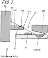
- FIGS. 7 to 13 show various examples of the positional relationship between the housing 3 and the light reception/emission element 5.
- Each drawing shows an enlarged part corresponding to part of the cross section of FIG. 2 .
- the broken lines shown in each drawing indicate imaginary lines described in the following description.
- An upper surface of the upper wall 31 may include a third inclined surface 313 approaching the lower surface thereof from the side wall 30 toward the first light passing portion 311. As a result, it is possible to reduce light which enters an inner surface of the first light passing portion 311 from the outside is partially reflected by the third inclined surface 313 and enters the first light receiving element 53. Therefore, the monitoring accuracy of the light reception/emission element module 1 can be improved.
- the upper wall 31 may include a first light shielding portion 31a located on an imaginary line connecting the third inclined surface 313 and the second region 532.
- the "light shielding portion” may be any one as long as the portion reduces the intensity of light passing therethrough, and is not limited to one that makes the intensity of light zero.
- the peripheral portion 330 includes the third inclined surface 313 on the upper surface thereof.
- a first imaginary line L1 connecting an upper end of the third inclined surface 313 and an edge of the second region 532 on the light emitting element 52 side is defined, an intersection of the third inclined surface 313 and the first light passing portion 311 is located above the first imaginary line L1. Therefore, the intersection of the third inclined surface 313 and the first light passing portion 311 functions as the first light shielding portion 31a.
- the upper surface of the upper wall 31 may include a fourth inclined surface 314 approaching the lower surface thereof from the side wall 30 toward the second light passing portion 312. As a result, it is possible to reduce the light entering the second light passing portion 312 and entering the first light receiving element 53 so as to improve the monitoring accuracy of the light reception/emission element module 1.
- the upper wall 31 may include a second light shielding portion 31b located on an imaginary line connecting the fourth inclined surface 314 and the second region 532.
- the peripheral portion 330 includes the fourth inclined surface 314 on the upper surface thereof. Further, when a second imaginary line L2 connecting an upper end of the fourth inclined surface 314 and the edge of the second region 532 on the second light receiving element 54 side is defined, an intersection of the fourth inclined surface 314 and the second light passing portion 312 is located above the second imaginary line L2. Therefore, the intersection of the fourth inclined surface 314 and the second light passing portion 312 functions as the second light shielding portion 31b.
- the lower surface of the intermediate portion 320 may include a third light shielding portion 31c located on an imaginary line connecting the inner surface of the first light passing portion 311 in the peripheral portion 330 and the second region 532.
- the side wall 30 may be located on an imaginary line connecting an upper end of the first light passing portion 311 in the peripheral portion 330 of the upper wall 31 and the second region 532. As a result, it is possible to reduce the light entering the first light passing portion 311 from the outside and entering the second region 532 so as to improve the monitoring accuracy of the light reception/emission element module 1.
- the intermediate portion 320 may include a fourth light shielding portion 31d located on an imaginary line connecting the inner surface of the second light passing portion 312 in the peripheral portion 330 and the second region 532. As a result, it is possible to reduce the light entering the second light passing portion 312 and entering the second region 532 so as to improve the monitoring accuracy of the light reception/emission element module 1.
- the intermediate portion 320 of the disclosure for example, as shown in FIG. 10 , when a fourth imaginary line L4 connecting an upper end of the inner surface of the second light passing portion 312 in the peripheral portion 330 and the edge of the second region 532 on the second light receiving element 54 side is defined, an intersection of the second light passing portion 312 and the second inclined surface 323 is located below the fourth imaginary line L4. Therefore, the intersection of the second light passing portion 312 and the second inclined surface 323 functions as the fourth light shielding portion 31d.
- the side wall 30 may be located on an imaginary line connecting an upper end of the second light passing portion 312 in the peripheral portion 330 of the upper wall 31 and the second region 532. As a result, it is possible to reduce the light entering the second light passing portion 312 from the outside and entering the second region 532 so as to improve the monitoring accuracy of the light reception/emission element module 1.
- the intermediate portion 320 may include a fifth light shielding portion 31e located on an imaginary line that inclines upward at the same angle as an imaginary line connecting the inner surface of the first light passing portion 311 in the peripheral portion 330 and the second region 532, with respect to the inner surface of the first light passing portion 311.
- a fifth light shielding portion 31e located on an imaginary line that inclines upward at the same angle as an imaginary line connecting the inner surface of the first light passing portion 311 in the peripheral portion 330 and the second region 532, with respect to the inner surface of the first light passing portion 311.
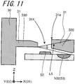
- the intermediate portion 320 of the disclosure for example, as shown in FIG. 11 , when a fifth imaginary line L5 that inclines upward at the same angle as an imaginary line connecting the lower end of the inner surface of the first light passing portion 311 in the peripheral portion 330 and the edge of the second region 532 on the second light receiving element 54 side, with respect to the inner surface of the first light passing portion 311 is defined, an intersection of the upper end of the first light passing portion 311 and the upper surface of the upper wall 31 (the intermediate portion 320) is located above the fifth imaginary line L5. Therefore, the intersection of the upper end of the first light passing portion 311 and the upper surface of the upper wall 31 functions as the fifth light shielding portion 31e.
- the intermediate portion 320 may include a sixth light shielding portion 31f located on an imaginary line that inclines upward at the same angle as an imaginary line connecting the inner surface of the second light passing portion 312 in the peripheral portion 330 and the second region 532, with respect to the inner surface of the second light passing portion 312.
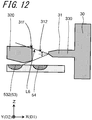
- the intermediate portion 320 of the disclosure for example, as shown in FIG. 12 , when a sixth imaginary line L6 that inclines upward at the same angle as an imaginary line connecting the lower end of the inner surface of the second light passing portion 312 in the peripheral portion 330 and the edge of the second region 532 on the second light receiving element 54 side, with respect to the inner surface of the second light passing portion 312 is defined, an intersection of the upper end of the second light passing portion 312 and the upper surface of the upper wall 31 (the intermediate portion 320) is located above the sixth imaginary line L6. Therefore, the intersection of the upper end of the second light passing portion 312 and the upper surface of the upper wall 31 functions as the sixth light shielding portion 31f.
- the intermediate portion 320 may include a seventh light shielding portion 31g located on an imaginary line connecting the top portion 324 of the lower surface and the second region 532. As a result, the monitoring accuracy of the light reception/emission element module 1 can be improved.
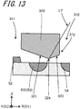
- the intersection of the second light passing portion 312 and the second inclined surface 323 is located below the imaginary line L7. Therefore, the intersection of the second light passing portion 312 and the second inclined surface 323 functions as the seventh light shielding portion 31g.
- the inner surface of the second light passing portion 312 may have a fifth inclined surface 315 which is inclined away from the first light receiving element 53 from the upper end to the lower end thereof.
- the housing 3 can be formed by, for example, a general-purpose plastic such as polypropylene resin (PP), polystyrene resin (PS), vinyl chloride resin (PVC), polyethylene terephthalate resin (PET), and acrylonitrile-butadiene-styrene resin (ABS), an engineering plastic such as polyamide resin (PA) and poly-carbonate resin (PC), a super engineering plastic such as liquid crystal polymer, and a metal material such as aluminum (Al) and titanium (Ti).
- PP polypropylene resin
- PS polystyrene resin
- PVC vinyl chloride resin
- PET polyethylene terephthalate resin
- ABS acrylonitrile-butadiene-styrene resin
- an engineering plastic such as polyamide resin (PA) and poly-carbonate resin (PC)
- PC poly-carbonate resin
- a super engineering plastic such as liquid crystal polymer
- a metal material such as aluminum (Al) and titanium (Ti).
- the lens member 4 can guide the light from the light emitting element 52 to the object, or can guide the reflected light from the object to the second light receiving element 54.
- the lens member 4 includes a lens portion 41 through which light passes and a support portion 42 which supports the lens portion 41, as shown in FIGS. 1 and 2 .
- the lens member 4 is fitted in a region surrounded by the inner surface of the side wall 30 of the housing 3 and the upper surface of the upper wall 31 via the support portion 42.
- the lens member 4 can be formed of a light-transmittable material.
- the lens member 4 can be made of, for example, plastics such as thermosetting resin such as silicone resin, urethane resin, and epoxy resin, or thermoplastic resin such as polycarbonate resin and acrylic resin, or sapphire and inorganic glass.
- the lens member 4 can be formed, for example, by injection molding or otherwise.
- the lens portion 41 can condense and guide the emitted light from the light emitting element 52 and the reflected light from the object.
- the lens portion 41 include a first lens 43 for condensing the emitted light from the light emitting element 52 and a second lens 44 for condensing the reflected light from the object.
- a convex lens, a spherical lens, or an aspheric lens can be used as each of the first lens 43 and the second lens 44 of the disclosure.
- the support portion 42 can hold the lens portion 41.
- the support portion 42 can be formed in a plate shape, for example.
- the support portion 42 may hold the lens portion 41 by being formed integrally with the lens portion 41, or may hold the lens portion 41 by fitting the first lens 43 and the second lens 44 of the lens portion 41 into the support portion 42.
- the first light receiving element 53 and the second light receiving element 54 of the disclosure have part of the substrate 51 as a component, but the substrate 51 according to the disclosure may not comprise part of the first light receiving element 53 and the second light receiving element 54.
- the light receiving elements instead of the substrate 51, the light receiving elements may be individually mounted on the substrate by using the wiring substrate 2 as a substrate. Also, in this case, the light emitting elements may be separately mounted.
- the region excluding the region of the second conductivity type is of the first conductivity type, but it is sufficient that only the portion that functions as a light receiving element is of the first conductivity type.
- first light receiving element 53 and the second light receiving element 54 of the disclosure are PN junctions, but may be PIN junctions including a third conductivity type.
- the first light receiving element 53 of the disclosure is disposed in the region between the light emitting element 52 and the second light receiving element 54.
- the first light receiving element 53 may not be disposed in the region between the light emitting element 52 and the second light receiving element 54 as long as the light of the light emitting element 52 can be monitored.
- the light emitting element 52 may be disposed in the region between the first light receiving element 53 and the second light receiving element 54.
- the case where a single light emitting element 52 is provided is described in the above-described embodiment, but a plurality of light emitting elements 52 may be provided. Further, the first light receiving element 53 and the second light receiving element 54 may be provided according to the number of the light emitting elements 52.
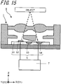
- the sensor device 6 of the disclosure includes the light reception/emission element module 1 and a control circuit 7 which is electrically connected to the light reception/emission element module 1.
- the control circuit 7 can control the light reception/emission element module 1.
- the control circuit 7 includes, for example, a drive circuit for driving the light reception/emission element 5, an arithmetic circuit for processing the current of the light reception/emission element 5, or a communication circuit for communicating with an external device.
- the broken arrow shown in FIG. 15 exemplifies a path of light which is emitted from the light emitting element 52, is reflected by the object, and enters the second light receiving element 54.
Landscapes
- Physics & Mathematics (AREA)
- Engineering & Computer Science (AREA)
- General Physics & Mathematics (AREA)
- Electromagnetism (AREA)
- Computer Networks & Wireless Communication (AREA)
- Radar, Positioning & Navigation (AREA)
- Remote Sensing (AREA)
- Life Sciences & Earth Sciences (AREA)
- General Life Sciences & Earth Sciences (AREA)
- Geophysics (AREA)
- Photo Coupler, Interrupter, Optical-To-Optical Conversion Devices (AREA)
- Led Device Packages (AREA)
Abstract
Description
- The present disclosure relates to a light reception/emission element module and a sensor device.
- In the related art, as a light reception/emission element module, a reflection type optical coupling device in which a light emitting portion and a light receiving portion are mounted on a substrate is disclosed (see, for example, Patent Literature 1).
- Patent Literature 1: Japanese Unexamined Patent Publication
JP-A 5-152603(1993) - In a light reception/emission element module, it is required to monitor the intensity of light emission in a light emitting portion.
- The light reception/emission element module of the disclosure comprises a substrate, a light emitting element that is disposed on the substrate, a first light receiving element that is disposed on the substrate apart from the light emitting element, and an upper wall that is located above the substrate. The upper wall comprises a facing surface facing the light emitting element and the first light receiving element.
- In the light reception/emission element module of the disclosure, the intensity of light emission in a light emitting portion can be monitored.
-
-
FIG. 1 is a perspective view of a light reception/emission element module of the disclosure; -
FIG. 2 is a cross-sectional view of the light reception/emission element module of the disclosure; -
FIG. 3 is an enlarged view of part of a cross section of the light reception/emission element module of the disclosure; -
FIG. 4 is an enlarged view of part of a cross section of the light reception/emission element module of the disclosure; -
FIG. 5 is a top view of the light reception/emission element module of the disclosure; -
FIG. 6 is a top view of the light reception/emission element module of the disclosure; -
FIG. 7 is an enlarged view of part of a cross section of the light reception/emission element module of the disclosure; -
FIG. 8 is an enlarged view of part of a cross section of the light reception/emission element module of the disclosure; -
FIG. 9 is an enlarged view of part of a cross section of the light reception/emission element module of the disclosure; -
FIG. 10 is an enlarged view of part of a cross section of the light reception/emission element module of the disclosure; -
FIG. 11 is an enlarged view of part of a cross section of the light reception/emission element module of the disclosure; -
FIG. 12 is an enlarged view of part of a cross section of the light reception/emission element module of the disclosure; -
FIG. 13 is an enlarged view of part of a cross section of the light reception/emission element module of the disclosure; -
FIG. 14 is a cross-sectional view showing an overview of the light reception/emission element module of the disclosure; and -
FIG. 15 is a cross-sectional view showing an overview of a sensor device of the disclosure. - Hereinafter, a light reception/emission element module of the disclosure will be described with reference to drawings. In the following description, for convenience, an orthogonal coordinate system (X, Y, and Z) is defined, and the positive side in a Z-axis direction is upward, but in the light reception/emission element module of the disclosure, any direction may be upward or downward. A first direction D1 described in the following description is a direction along an X axis, and a second direction D2 is a direction along a Y axis.
-
FIGS. 1 and2 schematically show an example of a light reception/emission element module of the disclosure.FIG. 2 is a cross-sectional view of the light reception/emission element module shown inFIG. 1 taken along the line II-II. - A light reception/
emission element module 1 can sense an object, for example, by irradiating the object with light from a light emitting portion and detecting reflected light from the object with a light receiving portion. The light reception/emission element module 1 can be incorporated into an image forming apparatus such as a copier or a printer, for example, to detect position information, distance information, density information, and the like of an object such as toner or media. - As shown in
FIG. 1 , the light reception/emission element module 1 comprises awiring substrate 2, ahousing 3 disposed on thewiring substrate 2, and alens member 4 disposed on thehousing 3. Further, as shown inFIG. 2 , in thehousing 3, a light reception/emission element 5 mounted on thewiring substrate 2 is disposed. - The
wiring substrate 2 can support the light reception/emission element 5. Thewiring substrate 2 can be electrically connected to an external device to drive the light reception/emission element 5. For example, the light reception/emission element 5 may be mounted on thewiring substrate 2 and electrically connected by a bonding wire. - The
wiring substrate 2 may be formed, for example, in a rectangular shape. Thewiring substrate 2 can be formed, for example, by laminating an insulating layer and a wiring. Thewiring substrate 2 may be, for example, a resin substrate or a ceramic substrate. Thewiring substrate 2 of the disclosure is a resin substrate. The insulating layer of the resin substrate is a resin layer, and the insulating layer of the ceramic substrate is a ceramic layer. - The light reception/
emission element 5 can emit light and detect incident light. The light reception/emission element 5 comprises asubstrate 51, and alight emitting element 52, alight receiving element 54, and a plurality ofelectrodes 55 which are disposed on thesubstrate 51. Further, the light reception/emission element 5 comprises a firstlight receiving element 53 in addition to the light receiving element 54 (second light receiving element 54) in order to monitor the light emission intensity of thelight emitting element 52. Thelight emitting element 52 and the secondlight receiving element 54 are aligned along the first direction D1. The firstlight receiving element 53 is disposed in the region between thelight emitting element 52 and the secondlight receiving element 54. - The
substrate 51 can support thelight emitting element 52, and the firstlight receiving element 53 and the secondlight receiving element 54. Thesubstrate 51 may be made of, for example, a semiconductor material. Thesubstrate 51 may be, for example, a substrate of silicon (Si) crystal. Thesubstrate 51 may have, for example, a plate shape. The thickness of thesubstrate 51 may be, for example, 300 µm or more and 400 µm or less. The planar shape of thesubstrate 51 may be, for example, a rectangular shape. Thesubstrate 51 can be formed, for example, by slicing an ingot of silicon (Si) into a wafer. - The outline of the
light emitting element 52 is schematically shown inFIG. 3. FIG. 3 is an enlarged view of thelight emitting element 52 in the cross section ofFIG. 2 . - The
light emitting element 52 can emit light when a voltage is applied. Thelight emitting element 52 may be, for example, a light emitting diode (LED) or a laser diode (LD). Thelight emitting element 52 includes a plurality ofsemiconductor layers 520 disposed on an upper surface of thesubstrate 51, and afirst electrode 551 and asecond electrode 552 for applying a voltage to the plurality ofsemiconductor layers 520. - The plurality of semiconductor layers 520 includes a first semiconductor layer 521 of a first conductivity type, a second semiconductor layer 522 of a second conductivity type, and a
third semiconductor layer 523. Thethird semiconductor layer 523 is located between the first semiconductor layer 521 and the second semiconductor layer 522. - The first semiconductor layer 521 is electrically connected to the
first electrode 551. The second semiconductor layer 522 is electrically connected to thesecond electrode 552. When a voltage is applied by thefirst electrode 551 and thesecond electrode 552, carriers such as electrons and holes flow into thethird semiconductor layer 523 through the first semiconductor layer 521 and the second semiconductor layer 522, and thethird semiconductor layer 523 can emit light. - The first semiconductor layer 521 includes a first contact layer 521a and a
first cladding layer 521b stacked on the first contact layer 521a. In addition to thefirst cladding layer 521b, thefirst electrode 551 is also disposed on an upper surface of the first contact layer 521a. Thethird semiconductor layer 523 is stacked on thefirst cladding layer 521b. - The first contact layer 521a can reduce the electrical contact resistance with the
first electrode 551. The first contact layer 521a may be made of, for example, gallium arsenide (GaAs) containing an n-type impurity. The n-type impurity of the first contact layer 521a may be, for example, silicon (Si) or selenium (Se). The thickness of the first contact layer 521a is, for example, 0.8 µm or more and 1 µm or less. - In the present specification, the "first conductivity type" is defined as "n-type", and the "second conductivity type" is defined as "p-type". However, in the present invention, "first conductivity type" may be defined as "p-type". In this case, the "second conductivity type" is defined as "n-type".
- The
first cladding layer 521b can confine holes in thethird semiconductor layer 523. Thefirst cladding layer 521b may be made of, for example, aluminum gallium arsenide (AlGaAs) containing an n-type impurity. The n-type impurity of thefirst cladding layer 521b may be, for example, silicon (Si) or selenium (Se). The thickness of thefirst cladding layer 521b is, for example, 0.2 µm or more and 0.5 µm or less. - The second semiconductor layer 522 includes a
second cladding layer 522a stacked on thethird semiconductor layer 523 and asecond contact layer 522b stacked on thesecond cladding layer 522a. Thesecond electrode 552 is disposed on an upper surface of thesecond contact layer 522b. - The
second cladding layer 522a has a function of confining electrons in thethird semiconductor layer 523. Thesecond cladding layer 522a may be made of, for example, aluminum gallium arsenide (AlGaAs) containing a p-type impurity. The p-type impurity of thesecond cladding layer 522a may be, for example, zinc (Zn) or magnesium (Mg). The thickness of thesecond cladding layer 522a is, for example, 0.2 µm or more and 0.5 µm or less. - The
second contact layer 522b has a function of reducing the electrical contact resistance with thesecond electrode 552. Thesecond contact layer 522b may be made of, for example, aluminum gallium arsenide (AlGaAs) containing a p-type impurity. The thickness of thesecond contact layer 522b may be, for example, 0.2 µm or more and 0.5 µm or less. Thesecond contact layer 522b is set to have a carrier density higher than that of thesecond cladding layer 522a in order to reduce the contact resistance with the electrode. - The
third semiconductor layer 523 is a so-called active layer, and is a light emitting portion. Thethird semiconductor layer 523 can emit light by recombination of carriers. Thethird semiconductor layer 523 may be made of, for example, aluminum gallium arsenide (AlGaAs) or the like. The thickness of thethird semiconductor layer 523 is, for example, 0.1 µm or more and 0.5 µm or less. - An insulating
layer 56 is disposed on the surface of the plurality ofsemiconductor layers 520 except for connection portions with the plurality ofelectrodes 55 for the purpose of preventing a short circuit between the plurality ofelectrodes 55. - In addition, the plurality of
semiconductor layers 520 may further include a fourth semiconductor layer 524 stacked on the upper surface of thesubstrate 51. The fourth semiconductor layer 524 can function as a buffer layer of the plurality of semiconductor layers 520. The fourth semiconductor crucible 524 may be made of, for example, gallium arsenide (GaAs) or the like. The thickness of the fourth semiconductor layer 524 is, for example, 2 µm or more and 3 µm or less. - As described above, the plurality of
semiconductor layers 520 are stacked and formed on the upper surface of thesubstrate 51 in the order of the fourth semiconductor layer 524, the first semiconductor layer 521, thethird semiconductor layer 523, and the second semiconductor layer 522. The plurality ofsemiconductor layers 520 can be formed by epitaxial growth sequentially on the upper surface of thesubstrate 51 by using, for example, a metal organic chemical vapor deposition (MOCVD) method. Further, the insulatinglayer 56 can be formed, for example, by using a plasma chemical vapor deposition (P-CVD) method. The plurality ofelectrodes 55 can be formed, for example, by using a vapor deposition method, a sputtering method, a plating method, or the like. -
FIGS. 4 and 5 show an outline of the light reception/emission element 5. InFIGS. 4 and 5 , thewiring substrate 2, thehousing 3, and thelens member 4 are not illustrated. - The first
light receiving element 53 can receive light and convert the light into a current. The firstlight receiving element 53 receives light prior to being reflected by the object among the light emitted from thelight emitting element 52. As a result, the firstlight receiving element 53 can monitor the intensity of light emission of thelight emitting element 52. The firstlight receiving element 53 may be, for example, a photo diode (PD) or a photo transistor (PT). - The first
light receiving element 53, as shown inFIGS. 4 and 5 , includes afirst region 531 of the first conductivity type, asecond region 532 of the second conductivity type, athird electrode 553 connected to thefirst region 531, and afourth electrode 554 connected to thesecond region 532. The firstlight receiving element 53 forms a pn junction with thefirst region 531 and thesecond region 532 and can convert incident light into a current. Thethird electrode 553 and thefourth electrode 554 can extract a current obtained by converting incident light. - In the first
light receiving element 53 of the disclosure, part of thesubstrate 51 comprises thefirst region 531 and thesecond region 532. In other words, thesubstrate 51 includes thefirst region 531 and thesecond region 532. That is, a pn junction is formed by replacing part of thesubstrate 51 of the first conductivity type with the second conductivity type and functions as part of the firstlight receiving element 53. Thefirst region 531 and thesecond region 532 comprises part of the surface of thesubstrate 51, and are electrically connected to thethird electrode 553 and thefourth electrode 554 disposed on the surface of thesubstrate 51. In the firstlight receiving element 53 of the disclosure, thesecond region 532 comprises part of the upper surface of thesubstrate 51, and serves as a light receiving region. - Since the
substrate 51 of the disclosure forms a pn junction, thesubstrate 51 has n-type or p-type impurities. The n-type impurity of thesubstrate 51 may be, for example, phosphorus (P) or nitrogen (N). The p-type impurity of thesubstrate 51 may be, for example, boron (B), zinc (Zn), magnesium (Mg) or the like. After doping thesubstrate 51 with an n-type impurity, thefirst region 531 and thesecond region 532 can be formed by further doping the p-type impurity. - The
second receiver element 54 can receive light and convert the light into a current. Unlike the firstlight receiving element 53, the secondlight receiving element 54 receives the light reflected by the object among the light emitted from thelight emitting element 52. As a result, the surface condition of the object can be measured. The secondlight receiving element 54 may be, for example, PD or PT. - The second
light receiving element 54, as shown inFIGS. 4 and 5 , includes athird region 541 of the first conductivity type, afourth region 542 of the second conductivity type, afifth electrode 555 connected to thethird region 541, and asixth electrode 556 connected to thefourth region 542. The secondlight receiving element 54 forms a pn junction with thethird region 541 and thefourth region 542 and can convert incident light into a current. Thefifth electrode 555 and thesixth electrode 556 can extract a current obtained by converting incident light. - In the second
light receiving element 54 of the disclosure, part of thesubstrate 51 comprises thethird region 541 and thefourth region 542. In other words, thesubstrate 51 includes thethird region 541 and thefourth region 542. That is, a pn junction is formed by replacing part of thesubstrate 51 of the first conductivity type with the second conductivity type and functions as part of the secondlight receiving element 54. Thethird region 541 and thefourth region 542 comprise part of the surface of thesubstrate 51 and are electrically connected to thefifth electrode 555 and thesixth electrode 556 disposed on the surface of thesubstrate 51. In the secondlight receiving element 54 of the disclosure, thefourth region 542 comprises part of the upper surface of thesubstrate 51, and serves as a light receiving region. Further, in the firstlight receiving element 53 and the secondlight receiving element 54 of the disclosure, thefirst region 531 and thethird region 541 are the same. In other words, the firstlight receiving element 53 and the secondlight receiving element 54 share the region of the first conductivity type. - The
third electrode 553 and thefourth electrode 554 of the firstlight receiving element 53 may be drawn out in the second direction D2 orthogonal to the first direction D1. As a result, the noise current from thelight emitting element 52 can be reduced. - Furthermore, the
third electrode 553 and thefourth electrode 554 of the firstlight receiving element 53 may be located on the opposite side of thelight emitting element 52 along the first direction D1. As a result, the noise current from thelight emitting element 52 can be reduced. - The
third electrode 553 and thefourth electrode 554 of the firstlight receiving element 53 may be located in the region between the firstlight receiving element 53 and the secondlight receiving element 54. As a result, for example, when connecting to thewiring substrate 2 by a bonding wire or the like, a wire or the like is located in a region between the firstlight receiving element 53 and the secondlight receiving element 54. Therefore, it is possible to reduce the light entering the firstlight receiving element 53 from the outside. - Further, the
fifth electrode 555 and thesixth electrode 556 of the secondlight receiving element 54 may be located in the region between the firstlight receiving element 53 and the secondlight receiving element 54. As a result, it is possible to reduce the light entering thefirst receiver element 53 from the outside. - The
fifth electrode 555 and thesixth electrode 556 of the secondlight receiving element 54 may be located in a region excluding the region between the firstlight receiving element 53 and the secondlight receiving element 54. - The
housing 3 can protect the light reception/emission element 5. Further, thehousing 3 can block or reduce light entering the light reception/emission element 5 from the outside. - As shown in
FIG. 2 , thehousing 3 includes aside wall 30 which surrounds the light reception/emission element 5 and anupper wall 31 which is connected to theside wall 30 and is located above the light reception/emission element 5 so as to cover a region surrounded by theside wall 30. The light reception/emission element 5 is disposed in a region surrounded by an inner surface of theside wall 30 and a lower surface of theupper wall 31. Theside wall 30 may have, for example, a frame shape, and theupper wall 31 may have, for example, a plate shape. A lower surface of theside wall 30 of thehousing 3 may be connected to an upper surface of thewiring substrate 2 via, for example, an adhesive. Theupper wall 31 is disposed midway in the height direction of theside wall 30. - As shown in
FIGS. 2 and6 , theupper wall 31 comprises a plurality of light passingportions 310, and the plurality of light passingportions 310 allow the light emitted or received by the light reception/emission element 5 to pass through thehousing 3. The plurality of light passingportions 310 of the disclosure are a plurality of through holes provided in theupper wall 31. The plurality of light passingportions 310 include a firstlight passing portion 311 located above thelight emitting element 52 and a secondlight passing portion 312 located above the secondlight receiving element 54. The emitted light of thelight emitting element 52 passes through the firstlight passing portion 311, and the reflected light from the object passes through the secondlight passing portion 312. -
FIG. 6 shows an outline of thehousing 3. InFIG. 6 , thewiring substrate 2 and thelens member 4 are not illustrated. - The
upper wall 31 of thehousing 3 further comprises anintermediate portion 320 located between the plurality of light passingportions 310 and aperipheral portion 330 surrounding the plurality of light passingportions 310 and theintermediate portion 320. Theintermediate portion 320 is located in the region between the light emittingelement 52 and the secondlight receiving element 54, and it is possible to divide the region through which the light emitted from thelight emitting element 52 passes and the region through which the light received by the secondlight receiving element 54 passes. Theperipheral portion 330 can reduce unnecessary light incident from the outside. - In
FIG. 6 , a region surrounded by the plurality of light passingportions 310 and dotted lines is theintermediate portion 320, and a region located outside the dotted lines and surrounding the plurality of light passingportions 310 is theperipheral portion 330. - The
intermediate portion 320 is located above the firstlight receiving element 53, as shown inFIG. 2 . Theintermediate portion 320 includes a facingsurface 321 facing thelight emitting element 52 and the firstlight receiving element 53. As a result, the light reception/emission element module 1 can reflect the light entering the facingsurface 321 among the light from thelight emitting element 52 to the firstlight receiving element 53. Therefore, the light reception/emission element module 1 can monitor the emission intensity of thelight emitting element 52 with the firstlight receiving element 53. - Further, the
intermediate portion 320 includes the facingsurface 321, and therefore, the light reception/emission element module 1 can reflect part of light emitted from thelight emitting element 52 to the firstlight receiving element 53. Therefore, since it is not necessary to newly provide another member for monitoring the light emission intensity of thelight emitting element 52, the light reception/emission element module 1 can be miniaturized. - The first
light receiving element 53 may receive regular reflection light by the facingsurface 321 for light emission from thelight emitting element 52, or may receive diffuse reflection light. In a case where the firstlight receiving element 53 receives regular reflection light, the intensity of the received light can be improved. In addition, in a case where the firstlight receiving element 53 receives the diffuse reflection light, the degree of freedom in design of the facingsurface 321 can be improved. - The facing
surface 321 may have any arrangement and shape as long as the light from thelight emitting element 52 can directly enter and can be reflected to the firstlight receiving element 53. - The
intermediate portion 320 includes alower surface 322 facing thesubstrate 51. Thelower surface 322 may include a firstinclined surface 321 which is inclined toward thelight emitting element 52, with respect to the upper surface of thesubstrate 51. In this case, the firstinclined surface 321 is the facingsurface 321. As a result, compared to the case where thelower surface 322 of theintermediate portion 320 extends along the upper surface of thesubstrate 51, the incident angle of the light of thelight emitting element 52 on the facingsurface 321 can be reduced, and the firstlight receiving element 53 can be disposed near thelight emitting element 52. Therefore, the light reception/emission element module 1 can be miniaturized. - The angle of the first
inclined surface 321 with respect to the upper surface of thesubstrate 51 may be any angle as long as the light from thelight emitting element 52 can be reflected to the firstlight receiving element 53. The firstlight receiving element 53 may be disposed anywhere as long as the firstlight receiving element 53 can receive the reflected light from the firstinclined surface 321. - The
lower surface 322 of theintermediate portion 320 may include a secondinclined surface 323 inclined toward the secondlight receiving element 54, with respect to the upper surface of thesubstrate 51. As a result, it is possible to reduce the light entering the secondlight receiving element 54 from thelight emitting element 52 without passing through the object. - The
lower surface 322 of theintermediate portion 320 may include atop portion 324 protruding downward. Thetop portion 324 may be located between the firstlight receiving element 53 and the secondlight receiving element 54. As a result, it is possible to reduce the light entering the secondlight receiving element 54 from thelight emitting element 52 without passing through the object. In a case where thelower surface 322 includes the firstinclined surface 321 and the secondinclined surface 323, an intersection of the firstinclined surface 321 and the secondinclined surface 323 is thetop portion 324. In a case where thelower surface 322 includes only the firstinclined surface 321, an intersection between the firstinclined surface 321 and an inner surface of the secondlight passing portion 312 is thetop portion 324. - The portion of the
lower surface 322 of theintermediate portion 320 closest to the substrate 51 (the top portion 324) may be located above thelight emitting element 52, or may be located below an upper surface of the light emitting element 52 (a plurality of semiconductor layers 520). If part of thelower surface 322 of theintermediate portion 320 is located above thelight emitting element 52, the contact between theupper wall 31 and thesubstrate 51 can be prevented. On the other hand, if part of thelower surface 322 of theintermediate portion 320 is located below the upper surface of thelight emitting element 52, light entering the secondlight receiving element 54 from thelight emitting element 52 without passing through the object can be reduced. - In a case where the
lower surface 322 of theintermediate portion 320 includes the secondinclined surface 323, the secondinclined surface 323 may be located above an imaginary line connecting the upper surface of thelight emitting element 52 and thetop portion 324. As a result, it is possible to reduce the light entering the secondlight receiving element 54 from thelight emitting element 52 without passing through the object. - In the light reception/
emission element 5 of the disclosure, a distance between the emittingelement 52 and the firstlight receiving element 53 is set to be larger than a distance between the secondlight receiving element 54 and the firstlight receiving element 53. - An edge of the first
light passing portion 311 may be located outside thesecond region 532 of the firstlight receiving element 53 in a planar direction as shown inFIGS. 2 and6 . As a result, light entering the firstlight receiving element 53 from the outside can be reduced. - The edge of the first
light passing portion 311 may be located in the region between the light emitting element 52 (the plurality of semiconductor layers 520) and the first light receiving element 53 (the second region 532) in the planar direction. As a result, the light quantity of thelight emitting element 52 extracted from the light reception/emission element module 1 can be increased. - An edge of the second
light passing portion 312 may be located outside thesecond region 532 of the firstlight receiving element 53 in the planar direction, as shown inFIGS. 2 and6 . As a result, light entering the firstlight receiving element 53 from the outside can be reduced. -
FIGS. 7 to 13 show various examples of the positional relationship between thehousing 3 and the light reception/emission element 5. Each drawing shows an enlarged part corresponding to part of the cross section ofFIG. 2 . The broken lines shown in each drawing indicate imaginary lines described in the following description. - An upper surface of the
upper wall 31 may include a thirdinclined surface 313 approaching the lower surface thereof from theside wall 30 toward the firstlight passing portion 311. As a result, it is possible to reduce light which enters an inner surface of the firstlight passing portion 311 from the outside is partially reflected by the thirdinclined surface 313 and enters the firstlight receiving element 53. Therefore, the monitoring accuracy of the light reception/emission element module 1 can be improved. - Further, the
upper wall 31 may include a firstlight shielding portion 31a located on an imaginary line connecting the thirdinclined surface 313 and thesecond region 532. As a result, the monitoring accuracy of the light reception/emission element module 1 can be improved. The "light shielding portion" may be any one as long as the portion reduces the intensity of light passing therethrough, and is not limited to one that makes the intensity of light zero. - In the
upper wall 31 of the disclosure, for example, as shown inFIG. 7 , theperipheral portion 330 includes the thirdinclined surface 313 on the upper surface thereof. In addition, when a first imaginary line L1 connecting an upper end of the thirdinclined surface 313 and an edge of thesecond region 532 on thelight emitting element 52 side is defined, an intersection of the thirdinclined surface 313 and the firstlight passing portion 311 is located above the first imaginary line L1. Therefore, the intersection of the thirdinclined surface 313 and the firstlight passing portion 311 functions as the firstlight shielding portion 31a. - The upper surface of the
upper wall 31 may include a fourthinclined surface 314 approaching the lower surface thereof from theside wall 30 toward the secondlight passing portion 312. As a result, it is possible to reduce the light entering the secondlight passing portion 312 and entering the firstlight receiving element 53 so as to improve the monitoring accuracy of the light reception/emission element module 1. - In addition, the
upper wall 31 may include a secondlight shielding portion 31b located on an imaginary line connecting the fourthinclined surface 314 and thesecond region 532. As a result, the monitoring accuracy of the light reception/emission element module 1 can be improved. - In the
upper wall 31 of the disclosure, for example, as shown inFIG. 8 , theperipheral portion 330 includes the fourthinclined surface 314 on the upper surface thereof. Further, when a second imaginary line L2 connecting an upper end of the fourthinclined surface 314 and the edge of thesecond region 532 on the secondlight receiving element 54 side is defined, an intersection of the fourthinclined surface 314 and the secondlight passing portion 312 is located above the second imaginary line L2. Therefore, the intersection of the fourthinclined surface 314 and the secondlight passing portion 312 functions as the secondlight shielding portion 31b. - The lower surface of the
intermediate portion 320 may include a thirdlight shielding portion 31c located on an imaginary line connecting the inner surface of the firstlight passing portion 311 in theperipheral portion 330 and thesecond region 532. As a result, it is possible to reduce the light entering the firstlight passing portion 311 and entering thesecond region 532 so as to improve the monitoring accuracy of the light reception/emission element module 1. - For example, as shown in
FIG. 9 , in theintermediate portion 320 of the disclosure, when a third imaginary line L3 connecting an upper end of the inner surface of the firstlight passing portion 311 in theperipheral portion 330 and the edge of thesecond region 532 on the secondlight receiving element 54 side is defined, an intersection of the firstinclined surface 321 and the firstlight passing portion 311 is located below the third imaginary line L3. Therefore, the intersection of the firstinclined surface 321 and the firstlight passing portion 311 functions as the thirdlight shielding portion 31c. - The
side wall 30 may be located on an imaginary line connecting an upper end of the firstlight passing portion 311 in theperipheral portion 330 of theupper wall 31 and thesecond region 532. As a result, it is possible to reduce the light entering the firstlight passing portion 311 from the outside and entering thesecond region 532 so as to improve the monitoring accuracy of the light reception/emission element module 1. - The
intermediate portion 320 may include a fourthlight shielding portion 31d located on an imaginary line connecting the inner surface of the secondlight passing portion 312 in theperipheral portion 330 and thesecond region 532. As a result, it is possible to reduce the light entering the secondlight passing portion 312 and entering thesecond region 532 so as to improve the monitoring accuracy of the light reception/emission element module 1. - In the
intermediate portion 320 of the disclosure, for example, as shown inFIG. 10 , when a fourth imaginary line L4 connecting an upper end of the inner surface of the secondlight passing portion 312 in theperipheral portion 330 and the edge of thesecond region 532 on the secondlight receiving element 54 side is defined, an intersection of the secondlight passing portion 312 and the secondinclined surface 323 is located below the fourth imaginary line L4. Therefore, the intersection of the secondlight passing portion 312 and the secondinclined surface 323 functions as the fourthlight shielding portion 31d. - The
side wall 30 may be located on an imaginary line connecting an upper end of the secondlight passing portion 312 in theperipheral portion 330 of theupper wall 31 and thesecond region 532. As a result, it is possible to reduce the light entering the secondlight passing portion 312 from the outside and entering thesecond region 532 so as to improve the monitoring accuracy of the light reception/emission element module 1. - The
intermediate portion 320 may include a fifthlight shielding portion 31e located on an imaginary line that inclines upward at the same angle as an imaginary line connecting the inner surface of the firstlight passing portion 311 in theperipheral portion 330 and thesecond region 532, with respect to the inner surface of the firstlight passing portion 311. As a result, the monitoring accuracy of the light reception/emission element module 1 can be improved. - In the
intermediate portion 320 of the disclosure, for example, as shown inFIG. 11 , when a fifth imaginary line L5 that inclines upward at the same angle as an imaginary line connecting the lower end of the inner surface of the firstlight passing portion 311 in theperipheral portion 330 and the edge of thesecond region 532 on the secondlight receiving element 54 side, with respect to the inner surface of the firstlight passing portion 311 is defined, an intersection of the upper end of the firstlight passing portion 311 and the upper surface of the upper wall 31 (the intermediate portion 320) is located above the fifth imaginary line L5. Therefore, the intersection of the upper end of the firstlight passing portion 311 and the upper surface of theupper wall 31 functions as the fifthlight shielding portion 31e. - The
intermediate portion 320 may include a sixthlight shielding portion 31f located on an imaginary line that inclines upward at the same angle as an imaginary line connecting the inner surface of the secondlight passing portion 312 in theperipheral portion 330 and thesecond region 532, with respect to the inner surface of the secondlight passing portion 312. As a result, the monitoring accuracy of the light reception/emission element module 1 can be improved. - In the
intermediate portion 320 of the disclosure, for example, as shown inFIG. 12 , when a sixth imaginary line L6 that inclines upward at the same angle as an imaginary line connecting the lower end of the inner surface of the secondlight passing portion 312 in theperipheral portion 330 and the edge of thesecond region 532 on the secondlight receiving element 54 side, with respect to the inner surface of the secondlight passing portion 312 is defined, an intersection of the upper end of the secondlight passing portion 312 and the upper surface of the upper wall 31 (the intermediate portion 320) is located above the sixth imaginary line L6. Therefore, the intersection of the upper end of the secondlight passing portion 312 and the upper surface of theupper wall 31 functions as the sixthlight shielding portion 31f. - The
intermediate portion 320 may include a seventhlight shielding portion 31g located on an imaginary line connecting thetop portion 324 of the lower surface and thesecond region 532. As a result, the monitoring accuracy of the light reception/emission element module 1 can be improved. - In the
intermediate portion 320 of the disclosure, for example, as shown inFIG. 13 , when a seventh imaginary line L7 connecting thetop portion 324 of the lower surface and the edge of thesecond region 532 on the secondlight receiving element 54 side is defined, the intersection of the secondlight passing portion 312 and the secondinclined surface 323 is located below the imaginary line L7. Therefore, the intersection of the secondlight passing portion 312 and the secondinclined surface 323 functions as the seventhlight shielding portion 31g. - The inner surface of the second
light passing portion 312 may have a fifthinclined surface 315 which is inclined away from the firstlight receiving element 53 from the upper end to the lower end thereof. As a result, the monitoring accuracy of the light reception/emission element module 1 can be improved. - The
housing 3 can be formed by, for example, a general-purpose plastic such as polypropylene resin (PP), polystyrene resin (PS), vinyl chloride resin (PVC), polyethylene terephthalate resin (PET), and acrylonitrile-butadiene-styrene resin (ABS), an engineering plastic such as polyamide resin (PA) and poly-carbonate resin (PC), a super engineering plastic such as liquid crystal polymer, and a metal material such as aluminum (Al) and titanium (Ti). Thehousing 3 can be formed, for example, by injection molding or otherwise. - The
lens member 4 can guide the light from thelight emitting element 52 to the object, or can guide the reflected light from the object to the secondlight receiving element 54. Thelens member 4 includes alens portion 41 through which light passes and asupport portion 42 which supports thelens portion 41, as shown inFIGS. 1 and2 . Thelens member 4 is fitted in a region surrounded by the inner surface of theside wall 30 of thehousing 3 and the upper surface of theupper wall 31 via thesupport portion 42. - The
lens member 4 can be formed of a light-transmittable material. Thelens member 4 can be made of, for example, plastics such as thermosetting resin such as silicone resin, urethane resin, and epoxy resin, or thermoplastic resin such as polycarbonate resin and acrylic resin, or sapphire and inorganic glass. Thelens member 4 can be formed, for example, by injection molding or otherwise. - The
lens portion 41 can condense and guide the emitted light from thelight emitting element 52 and the reflected light from the object. Thelens portion 41 include afirst lens 43 for condensing the emitted light from thelight emitting element 52 and asecond lens 44 for condensing the reflected light from the object. For example, a convex lens, a spherical lens, or an aspheric lens can be used as each of thefirst lens 43 and thesecond lens 44 of the disclosure. - The
support portion 42 can hold thelens portion 41. Thesupport portion 42 can be formed in a plate shape, for example. Thesupport portion 42 may hold thelens portion 41 by being formed integrally with thelens portion 41, or may hold thelens portion 41 by fitting thefirst lens 43 and thesecond lens 44 of thelens portion 41 into thesupport portion 42. - The disclosure is not limited to the above-described embodiments, and various changes, improvements, and the like can be made without departing from the scope of the disclosure.
- The first
light receiving element 53 and the secondlight receiving element 54 of the disclosure have part of thesubstrate 51 as a component, but thesubstrate 51 according to the disclosure may not comprise part of the firstlight receiving element 53 and the secondlight receiving element 54. For example, instead of thesubstrate 51, the light receiving elements may be individually mounted on the substrate by using thewiring substrate 2 as a substrate. Also, in this case, the light emitting elements may be separately mounted. - Further, in the
substrate 51 of the disclosure, the region excluding the region of the second conductivity type is of the first conductivity type, but it is sufficient that only the portion that functions as a light receiving element is of the first conductivity type. - In addition, the first
light receiving element 53 and the secondlight receiving element 54 of the disclosure are PN junctions, but may be PIN junctions including a third conductivity type. - Further, the first
light receiving element 53 of the disclosure is disposed in the region between the light emittingelement 52 and the secondlight receiving element 54. However, the firstlight receiving element 53 may not be disposed in the region between the light emittingelement 52 and the secondlight receiving element 54 as long as the light of thelight emitting element 52 can be monitored. For example, as shown inFIG. 14 , thelight emitting element 52 may be disposed in the region between the firstlight receiving element 53 and the secondlight receiving element 54. - Moreover, the case where a single
light emitting element 52 is provided is described in the above-described embodiment, but a plurality oflight emitting elements 52 may be provided. Further, the firstlight receiving element 53 and the secondlight receiving element 54 may be provided according to the number of thelight emitting elements 52. - Next, a
sensor device 6 provided with the light reception/emission element 5 will be described. As shown inFIG. 15 , thesensor device 6 of the disclosure includes the light reception/emission element module 1 and acontrol circuit 7 which is electrically connected to the light reception/emission element module 1. Thecontrol circuit 7 can control the light reception/emission element module 1. Thecontrol circuit 7 includes, for example, a drive circuit for driving the light reception/emission element 5, an arithmetic circuit for processing the current of the light reception/emission element 5, or a communication circuit for communicating with an external device. The broken arrow shown inFIG. 15 exemplifies a path of light which is emitted from thelight emitting element 52, is reflected by the object, and enters the secondlight receiving element 54. -
- 1:
- Light reception/emission element module
- 2:
- Wiring substrate
- 3:
- Housing
- 4:
- Lens member
- 5:
- Light reception/emission element
- 6:
- Sensor device
- 7:
- Control circuit
Claims (14)
- A light reception/emission element module, comprising:a substrate;a light emitting element disposed on the substrate;a first light receiving device disposed on the substrate apart from the light emitting element; andan upper wall located above the substrate,the upper wall comprising a facing surface facing the light emitting element and the first light receiving element.
- The light reception/emission element module according to claim 1, further comprising:a second light receiving element disposed on the substrate,wherein the upper wall further comprises a first light passing portion located above the light emitting element, a second light passing portion located above the second light receiving element, and an intermediate portion located in a region between the first light passing portion and the second light passing portion, andat least part of a lower surface of the intermediate portion comprises the facing surface.
- The light reception/emission element module according to claim 2, wherein an upper surface of the upper wall comprises an inclined surface approaching a lower surface of the upper wall toward the first light passing portion.
- The light reception/emission element module according to claim 3, wherein the upper wall comprises a first light shielding portion which is located on an imaginary line connecting the inclined surface and a light receiving region of the first light receiving element.
- The light reception/emission element module according to claim 2, wherein an upper surface of the upper wall comprises an inclined surface approaching a lower surface of the upper wall toward the second light passing portion.
- The light reception/emission element module according to claim 5, wherein the upper wall comprises a second light shielding portion which is located on an imaginary line connecting the inclined surface and a light receiving region of the first light receiving element.
- The light reception/emission element module according to any one of claims 2 to 6, wherein the upper wall further comprises a peripheral portion surrounding the first light passing portion, the second light passing portion, and the intermediate portion, and
the intermediate portion comprises a third light shielding portion which is located on an imaginary line connecting an inner surface of the first light passing portion in the peripheral portion and a light receiving region of the first light receiving element. - The light reception/emission element module according to any one of claims 2 to 7, wherein the upper wall further comprises a peripheral portion surrounding the first light passing portion, the second light passing portion, and the intermediate portion, and
the intermediate portion comprises a fourth light shielding portion which is located on an imaginary line connecting an inner surface of the second light passing portion in the peripheral portion and a light receiving region of the first light receiving element. - The light reception/emission element module according to any one of claims 2 to 8, wherein the intermediate portion comprises a fifth light shielding portion which is located on an imaginary line that inclines upward at a same angle as an angle at which the imaginary line connecting an inner surface of the first light passing portion in the peripheral portion and a light receiving region of the first light receiving element inclines downward, with respect to the inner surface of the first light passing portion.
- The light reception/emission element module according to any one of claims 2 to 9, wherein the intermediate portion comprises a sixth light shielding portion which is located on an imaginary line that inclines upward at a same angle as an angle at which the imaginary line connecting an inner surface of the second light passing portion in the peripheral portion and a light receiving region of the first light receiving element inclines downward, with respect to the inner surface of the second light passing portion.
- The light reception/emission element module according to any one of claims 2 to 10, wherein the lower surface of the intermediate portion further comprises a top portion protruding downward, and
the intermediate portion comprises a seventh light shielding portion which is located on an imaginary line connecting the top portion and a light receiving region of the first light receiving element. - The light reception/emission element module according to any one of claims 2 to 11, further comprising:a side wall which surrounds the light emitting element and the first light receiving element, the upper wall being disposed midway in a height direction of the side wall,wherein the side wall is located on an imaginary line connecting an upper end of the first light passing portion and a light receiving region of the first light receiving element.
- The light reception/emission element module according to any one of claims 2 to 12, further comprising:a side wall which surrounds the light emitting element and the first light receiving element, the upper wall being disposed midway in a height direction of the side wall,wherein the side wall is located on an imaginary line connecting an upper end of the second light passing portion and a light receiving region of the first light receiving element.
- A sensor device, comprising:the light reception/emission element module according to any one of claims 1 to 13; anda control circuit which is connected to the light reception/emission element module and controls the light reception/emission element module.
Applications Claiming Priority (2)
| Application Number | Priority Date | Filing Date | Title |
|---|---|---|---|
| JP2017088706 | 2017-04-27 | ||
| PCT/JP2018/016726 WO2018199132A1 (en) | 2017-04-27 | 2018-04-25 | Light reception/emission element module and sensor device |
Publications (3)
| Publication Number | Publication Date |
|---|---|
| EP3618128A1 true EP3618128A1 (en) | 2020-03-04 |
| EP3618128A4 EP3618128A4 (en) | 2020-12-16 |
| EP3618128B1 EP3618128B1 (en) | 2022-09-28 |
Family
ID=63919174
Family Applications (1)
| Application Number | Title | Priority Date | Filing Date |
|---|---|---|---|
| EP18792230.7A Active EP3618128B1 (en) | 2017-04-27 | 2018-04-25 | Light reception/emission element module and sensor device |
Country Status (4)
| Country | Link |
|---|---|
| US (1) | US11145781B2 (en) |
| EP (1) | EP3618128B1 (en) |
| JP (1) | JP6960451B2 (en) |
| WO (1) | WO2018199132A1 (en) |
Families Citing this family (2)
| Publication number | Priority date | Publication date | Assignee | Title |
|---|---|---|---|---|
| WO2020121989A1 (en) * | 2018-12-14 | 2020-06-18 | 富士フイルム株式会社 | Structure, optical measurement device, method for producing structure, and composition |
| WO2024023225A1 (en) * | 2022-07-28 | 2024-02-01 | Ams International Ag | Sensor device, optoelectronic device and method for fabricating a sensor device |
Family Cites Families (12)
| Publication number | Priority date | Publication date | Assignee | Title |
|---|---|---|---|---|
| JPH05152603A (en) | 1991-11-28 | 1993-06-18 | Sharp Corp | Reflection type photocoupler |
| JP5254833B2 (en) * | 2009-02-06 | 2013-08-07 | スタンレー電気株式会社 | Optical sensor |
| JP5805301B2 (en) * | 2011-04-15 | 2015-11-04 | オスラム オプト セミコンダクターズ ゲゼルシャフト ミット ベシュレンクテル ハフツングOsram Opto Semiconductors GmbH | Optoelectronic device |
| WO2015136099A2 (en) * | 2014-03-14 | 2015-09-17 | Mesa Imaging Ag | Optical imaging modules and optical detection modules including a time-of-flight sensor |
| US9746557B2 (en) | 2014-07-25 | 2017-08-29 | Heptagon Micro Optics Pte. Ltd. | Proximity sensor module including time-of-flight sensor wherein a second group of light sensitive elements is in a second one of the chambers of the module |
| US10128222B2 (en) | 2014-09-24 | 2018-11-13 | Kyocera Corporation | Light-emitting-and-receiving element module and sensor device using the same |
| JP2016134532A (en) * | 2015-01-20 | 2016-07-25 | 新日本無線株式会社 | Reflective sensor device and manufacturing method thereof |
| US20160307881A1 (en) * | 2015-04-20 | 2016-10-20 | Advanced Semiconductor Engineering, Inc. | Optical sensor module and method for manufacturing the same |
| JP6563722B2 (en) * | 2015-07-24 | 2019-08-21 | 京セラ株式会社 | Light emitting / receiving element module and sensor device |
| US10061057B2 (en) * | 2015-08-21 | 2018-08-28 | Stmicroelectronics (Research & Development) Limited | Molded range and proximity sensor with optical resin lens |
| JP2019016615A (en) * | 2015-12-01 | 2019-01-31 | シャープ株式会社 | Optical sensor and electronic apparatus including the same |
| JP6633197B2 (en) | 2016-06-01 | 2020-01-22 | シャープ株式会社 | Photodetector and electronic equipment |
-
2018
- 2018-04-25 US US16/605,461 patent/US11145781B2/en active Active
- 2018-04-25 EP EP18792230.7A patent/EP3618128B1/en active Active
- 2018-04-25 JP JP2019514559A patent/JP6960451B2/en active Active
- 2018-04-25 WO PCT/JP2018/016726 patent/WO2018199132A1/en not_active Ceased
Also Published As
| Publication number | Publication date |
|---|---|
| US11145781B2 (en) | 2021-10-12 |
| WO2018199132A1 (en) | 2018-11-01 |
| US20210126151A1 (en) | 2021-04-29 |
| JP6960451B2 (en) | 2021-11-05 |
| EP3618128B1 (en) | 2022-09-28 |
| JPWO2018199132A1 (en) | 2020-02-27 |
| EP3618128A4 (en) | 2020-12-16 |
Similar Documents
| Publication | Publication Date | Title |
|---|---|---|
| EP3291313B1 (en) | Light receiving and emitting element module and sensor device | |
| EP3086376B1 (en) | Light receiving/emitting element module and sensor device using same | |
| US10121930B2 (en) | Light receiving and emitting element module and sensor device using same | |
| US10128222B2 (en) | Light-emitting-and-receiving element module and sensor device using the same | |
| EP2701212B1 (en) | Light emitting diode | |
| JP6215728B2 (en) | Light emitting / receiving element module | |
| EP2755245A2 (en) | Light emitting device | |
| EP3618128B1 (en) | Light reception/emission element module and sensor device | |
| US9236544B2 (en) | Light emitting device | |
| EP2768032B1 (en) | Light emitting device | |
| JP6483531B2 (en) | Light emitting / receiving element module and sensor device | |
| JP6974208B2 (en) | Light receiving / receiving element module and sensor device | |
| JP7583641B2 (en) | Light emitting/receiving element, light emitting/receiving element module and sensor device | |
| JP6563722B2 (en) | Light emitting / receiving element module and sensor device | |
| EP2755244B1 (en) | Light emitting device | |
| JP2017135276A (en) | Light emitting / receiving element, light receiving / emitting element module and sensor device | |
| JP6616369B2 (en) | Light emitting / receiving element module | |
| KR20150144481A (en) | Light emitting device | |
| JP2017085022A (en) | Light emitting / receiving element, light receiving / emitting element module and sensor device | |
| KR20150144482A (en) | Light emitting device | |
| KR20150144483A (en) | Light emitting device |
Legal Events
| Date | Code | Title | Description |
|---|---|---|---|
| STAA | Information on the status of an ep patent application or granted ep patent |
Free format text: STATUS: THE INTERNATIONAL PUBLICATION HAS BEEN MADE |
|
| PUAI | Public reference made under article 153(3) epc to a published international application that has entered the european phase |
Free format text: ORIGINAL CODE: 0009012 |
|
| STAA | Information on the status of an ep patent application or granted ep patent |
Free format text: STATUS: REQUEST FOR EXAMINATION WAS MADE |
|
| 17P | Request for examination filed |
Effective date: 20191016 |
|
| AK | Designated contracting states |
Kind code of ref document: A1 Designated state(s): AL AT BE BG CH CY CZ DE DK EE ES FI FR GB GR HR HU IE IS IT LI LT LU LV MC MK MT NL NO PL PT RO RS SE SI SK SM TR |
|
| AX | Request for extension of the european patent |
Extension state: BA ME |
|
| DAV | Request for validation of the european patent (deleted) | ||
| DAX | Request for extension of the european patent (deleted) | ||
| REG | Reference to a national code |
Ref country code: DE Ref legal event code: R079 Ref document number: 602018041185 Country of ref document: DE Free format text: PREVIOUS MAIN CLASS: H01L0031120000 Ipc: H01L0031173000 |
|
| A4 | Supplementary search report drawn up and despatched |
Effective date: 20201117 |
|
| RIC1 | Information provided on ipc code assigned before grant |
Ipc: G01S 17/04 20200101ALI20201111BHEP Ipc: H01L 31/153 20060101ALI20201111BHEP Ipc: H03K 17/94 20060101ALI20201111BHEP Ipc: G01S 7/481 20060101ALI20201111BHEP Ipc: H01L 31/0224 20060101ALI20201111BHEP Ipc: H01L 31/12 20060101ALI20201111BHEP Ipc: G01V 8/12 20060101ALI20201111BHEP Ipc: H01L 31/173 20060101AFI20201111BHEP |
|
| GRAP | Despatch of communication of intention to grant a patent |
Free format text: ORIGINAL CODE: EPIDOSNIGR1 |
|
| STAA | Information on the status of an ep patent application or granted ep patent |
Free format text: STATUS: GRANT OF PATENT IS INTENDED |
|
| INTG | Intention to grant announced |
Effective date: 20220609 |
|
| GRAS | Grant fee paid |
Free format text: ORIGINAL CODE: EPIDOSNIGR3 |
|
| GRAA | (expected) grant |
Free format text: ORIGINAL CODE: 0009210 |
|
| STAA | Information on the status of an ep patent application or granted ep patent |
Free format text: STATUS: THE PATENT HAS BEEN GRANTED |
|
| AK | Designated contracting states |
Kind code of ref document: B1 Designated state(s): AL AT BE BG CH CY CZ DE DK EE ES FI FR GB GR HR HU IE IS IT LI LT LU LV MC MK MT NL NO PL PT RO RS SE SI SK SM TR |
|
| REG | Reference to a national code |
Ref country code: GB Ref legal event code: FG4D |
|
| REG | Reference to a national code |
Ref country code: CH Ref legal event code: EP |
|
| REG | Reference to a national code |
Ref country code: DE Ref legal event code: R096 Ref document number: 602018041185 Country of ref document: DE |
|
| REG | Reference to a national code |
Ref country code: AT Ref legal event code: REF Ref document number: 1521820 Country of ref document: AT Kind code of ref document: T Effective date: 20221015 |
|
| REG | Reference to a national code |
Ref country code: IE Ref legal event code: FG4D |
|
| REG | Reference to a national code |
Ref country code: LT Ref legal event code: MG9D |
|
| PG25 | Lapsed in a contracting state [announced via postgrant information from national office to epo] |
Ref country code: SE Free format text: LAPSE BECAUSE OF FAILURE TO SUBMIT A TRANSLATION OF THE DESCRIPTION OR TO PAY THE FEE WITHIN THE PRESCRIBED TIME-LIMIT Effective date: 20220928 Ref country code: RS Free format text: LAPSE BECAUSE OF FAILURE TO SUBMIT A TRANSLATION OF THE DESCRIPTION OR TO PAY THE FEE WITHIN THE PRESCRIBED TIME-LIMIT Effective date: 20220928 Ref country code: NO Free format text: LAPSE BECAUSE OF FAILURE TO SUBMIT A TRANSLATION OF THE DESCRIPTION OR TO PAY THE FEE WITHIN THE PRESCRIBED TIME-LIMIT Effective date: 20221228 Ref country code: LV Free format text: LAPSE BECAUSE OF FAILURE TO SUBMIT A TRANSLATION OF THE DESCRIPTION OR TO PAY THE FEE WITHIN THE PRESCRIBED TIME-LIMIT Effective date: 20220928 Ref country code: LT Free format text: LAPSE BECAUSE OF FAILURE TO SUBMIT A TRANSLATION OF THE DESCRIPTION OR TO PAY THE FEE WITHIN THE PRESCRIBED TIME-LIMIT Effective date: 20220928 Ref country code: FI Free format text: LAPSE BECAUSE OF FAILURE TO SUBMIT A TRANSLATION OF THE DESCRIPTION OR TO PAY THE FEE WITHIN THE PRESCRIBED TIME-LIMIT Effective date: 20220928 |
|
| REG | Reference to a national code |
Ref country code: NL Ref legal event code: MP Effective date: 20220928 |
|
| REG | Reference to a national code |
Ref country code: AT Ref legal event code: MK05 Ref document number: 1521820 Country of ref document: AT Kind code of ref document: T Effective date: 20220928 |
|
| PG25 | Lapsed in a contracting state [announced via postgrant information from national office to epo] |
Ref country code: HR Free format text: LAPSE BECAUSE OF FAILURE TO SUBMIT A TRANSLATION OF THE DESCRIPTION OR TO PAY THE FEE WITHIN THE PRESCRIBED TIME-LIMIT Effective date: 20220928 Ref country code: GR Free format text: LAPSE BECAUSE OF FAILURE TO SUBMIT A TRANSLATION OF THE DESCRIPTION OR TO PAY THE FEE WITHIN THE PRESCRIBED TIME-LIMIT Effective date: 20221229 |
|
| PG25 | Lapsed in a contracting state [announced via postgrant information from national office to epo] |
Ref country code: SM Free format text: LAPSE BECAUSE OF FAILURE TO SUBMIT A TRANSLATION OF THE DESCRIPTION OR TO PAY THE FEE WITHIN THE PRESCRIBED TIME-LIMIT Effective date: 20220928 Ref country code: RO Free format text: LAPSE BECAUSE OF FAILURE TO SUBMIT A TRANSLATION OF THE DESCRIPTION OR TO PAY THE FEE WITHIN THE PRESCRIBED TIME-LIMIT Effective date: 20220928 Ref country code: PT Free format text: LAPSE BECAUSE OF FAILURE TO SUBMIT A TRANSLATION OF THE DESCRIPTION OR TO PAY THE FEE WITHIN THE PRESCRIBED TIME-LIMIT Effective date: 20230130 Ref country code: ES Free format text: LAPSE BECAUSE OF FAILURE TO SUBMIT A TRANSLATION OF THE DESCRIPTION OR TO PAY THE FEE WITHIN THE PRESCRIBED TIME-LIMIT Effective date: 20220928 Ref country code: CZ Free format text: LAPSE BECAUSE OF FAILURE TO SUBMIT A TRANSLATION OF THE DESCRIPTION OR TO PAY THE FEE WITHIN THE PRESCRIBED TIME-LIMIT Effective date: 20220928 Ref country code: AT Free format text: LAPSE BECAUSE OF FAILURE TO SUBMIT A TRANSLATION OF THE DESCRIPTION OR TO PAY THE FEE WITHIN THE PRESCRIBED TIME-LIMIT Effective date: 20220928 |
|
| PG25 | Lapsed in a contracting state [announced via postgrant information from national office to epo] |
Ref country code: SK Free format text: LAPSE BECAUSE OF FAILURE TO SUBMIT A TRANSLATION OF THE DESCRIPTION OR TO PAY THE FEE WITHIN THE PRESCRIBED TIME-LIMIT Effective date: 20220928 Ref country code: PL Free format text: LAPSE BECAUSE OF FAILURE TO SUBMIT A TRANSLATION OF THE DESCRIPTION OR TO PAY THE FEE WITHIN THE PRESCRIBED TIME-LIMIT Effective date: 20220928 Ref country code: IS Free format text: LAPSE BECAUSE OF FAILURE TO SUBMIT A TRANSLATION OF THE DESCRIPTION OR TO PAY THE FEE WITHIN THE PRESCRIBED TIME-LIMIT Effective date: 20230128 Ref country code: EE Free format text: LAPSE BECAUSE OF FAILURE TO SUBMIT A TRANSLATION OF THE DESCRIPTION OR TO PAY THE FEE WITHIN THE PRESCRIBED TIME-LIMIT Effective date: 20220928 |
|
| P01 | Opt-out of the competence of the unified patent court (upc) registered |
Effective date: 20230508 |
|
| REG | Reference to a national code |
Ref country code: DE Ref legal event code: R097 Ref document number: 602018041185 Country of ref document: DE |
|
| PG25 | Lapsed in a contracting state [announced via postgrant information from national office to epo] |
Ref country code: NL Free format text: LAPSE BECAUSE OF FAILURE TO SUBMIT A TRANSLATION OF THE DESCRIPTION OR TO PAY THE FEE WITHIN THE PRESCRIBED TIME-LIMIT Effective date: 20220928 Ref country code: AL Free format text: LAPSE BECAUSE OF FAILURE TO SUBMIT A TRANSLATION OF THE DESCRIPTION OR TO PAY THE FEE WITHIN THE PRESCRIBED TIME-LIMIT Effective date: 20220928 |
|
| PG25 | Lapsed in a contracting state [announced via postgrant information from national office to epo] |
Ref country code: DK Free format text: LAPSE BECAUSE OF FAILURE TO SUBMIT A TRANSLATION OF THE DESCRIPTION OR TO PAY THE FEE WITHIN THE PRESCRIBED TIME-LIMIT Effective date: 20220928 |
|
| PLBE | No opposition filed within time limit |
Free format text: ORIGINAL CODE: 0009261 |
|
| STAA | Information on the status of an ep patent application or granted ep patent |
Free format text: STATUS: NO OPPOSITION FILED WITHIN TIME LIMIT |
|
| 26N | No opposition filed |
Effective date: 20230629 |
|
| PG25 | Lapsed in a contracting state [announced via postgrant information from national office to epo] |
Ref country code: SI Free format text: LAPSE BECAUSE OF FAILURE TO SUBMIT A TRANSLATION OF THE DESCRIPTION OR TO PAY THE FEE WITHIN THE PRESCRIBED TIME-LIMIT Effective date: 20220928 |
|
| REG | Reference to a national code |
Ref country code: CH Ref legal event code: PL |
|
| PG25 | Lapsed in a contracting state [announced via postgrant information from national office to epo] |
Ref country code: LU Free format text: LAPSE BECAUSE OF NON-PAYMENT OF DUE FEES Effective date: 20230425 |
|
| REG | Reference to a national code |
Ref country code: BE Ref legal event code: MM Effective date: 20230430 |
|
| PG25 | Lapsed in a contracting state [announced via postgrant information from national office to epo] |
Ref country code: MC Free format text: LAPSE BECAUSE OF FAILURE TO SUBMIT A TRANSLATION OF THE DESCRIPTION OR TO PAY THE FEE WITHIN THE PRESCRIBED TIME-LIMIT Effective date: 20220928 |
|
| PG25 | Lapsed in a contracting state [announced via postgrant information from national office to epo] |
Ref country code: MC Free format text: LAPSE BECAUSE OF FAILURE TO SUBMIT A TRANSLATION OF THE DESCRIPTION OR TO PAY THE FEE WITHIN THE PRESCRIBED TIME-LIMIT Effective date: 20220928 Ref country code: LI Free format text: LAPSE BECAUSE OF NON-PAYMENT OF DUE FEES Effective date: 20230430 Ref country code: FR Free format text: LAPSE BECAUSE OF NON-PAYMENT OF DUE FEES Effective date: 20230430 Ref country code: CH Free format text: LAPSE BECAUSE OF NON-PAYMENT OF DUE FEES Effective date: 20230430 |
|
| REG | Reference to a national code |
Ref country code: IE Ref legal event code: MM4A |
|
| PG25 | Lapsed in a contracting state [announced via postgrant information from national office to epo] |
Ref country code: BE Free format text: LAPSE BECAUSE OF NON-PAYMENT OF DUE FEES Effective date: 20230430 |
|
| PG25 | Lapsed in a contracting state [announced via postgrant information from national office to epo] |
Ref country code: IE Free format text: LAPSE BECAUSE OF NON-PAYMENT OF DUE FEES Effective date: 20230425 |
|
| PG25 | Lapsed in a contracting state [announced via postgrant information from national office to epo] |
Ref country code: IE Free format text: LAPSE BECAUSE OF NON-PAYMENT OF DUE FEES Effective date: 20230425 |
|
| PG25 | Lapsed in a contracting state [announced via postgrant information from national office to epo] |
Ref country code: IT Free format text: LAPSE BECAUSE OF FAILURE TO SUBMIT A TRANSLATION OF THE DESCRIPTION OR TO PAY THE FEE WITHIN THE PRESCRIBED TIME-LIMIT Effective date: 20220928 |
|
| PG25 | Lapsed in a contracting state [announced via postgrant information from national office to epo] |
Ref country code: BG Free format text: LAPSE BECAUSE OF FAILURE TO SUBMIT A TRANSLATION OF THE DESCRIPTION OR TO PAY THE FEE WITHIN THE PRESCRIBED TIME-LIMIT Effective date: 20220928 |
|
| REG | Reference to a national code |
Ref country code: DE Ref legal event code: R079 Ref document number: 602018041185 Country of ref document: DE Free format text: PREVIOUS MAIN CLASS: H01L0031173000 Ipc: H10F0055255000 |
|
| PG25 | Lapsed in a contracting state [announced via postgrant information from national office to epo] |
Ref country code: BG Free format text: LAPSE BECAUSE OF FAILURE TO SUBMIT A TRANSLATION OF THE DESCRIPTION OR TO PAY THE FEE WITHIN THE PRESCRIBED TIME-LIMIT Effective date: 20220928 |
|
| PGFP | Annual fee paid to national office [announced via postgrant information from national office to epo] |
Ref country code: GB Payment date: 20250306 Year of fee payment: 8 |
|
| PGFP | Annual fee paid to national office [announced via postgrant information from national office to epo] |
Ref country code: DE Payment date: 20250305 Year of fee payment: 8 |
|
| PG25 | Lapsed in a contracting state [announced via postgrant information from national office to epo] |
Ref country code: CY Free format text: LAPSE BECAUSE OF FAILURE TO SUBMIT A TRANSLATION OF THE DESCRIPTION OR TO PAY THE FEE WITHIN THE PRESCRIBED TIME-LIMIT; INVALID AB INITIO Effective date: 20180425 |
|
| PG25 | Lapsed in a contracting state [announced via postgrant information from national office to epo] |
Ref country code: HU Free format text: LAPSE BECAUSE OF FAILURE TO SUBMIT A TRANSLATION OF THE DESCRIPTION OR TO PAY THE FEE WITHIN THE PRESCRIBED TIME-LIMIT; INVALID AB INITIO Effective date: 20180425 |
|
| PG25 | Lapsed in a contracting state [announced via postgrant information from national office to epo] |
Ref country code: TR Free format text: LAPSE BECAUSE OF FAILURE TO SUBMIT A TRANSLATION OF THE DESCRIPTION OR TO PAY THE FEE WITHIN THE PRESCRIBED TIME-LIMIT Effective date: 20220928 |