EP3618105A1 - Integrating silicon-bjt to a silicon-germanium-hbt manufacturing process - Google Patents
Integrating silicon-bjt to a silicon-germanium-hbt manufacturing process Download PDFInfo
- Publication number
- EP3618105A1 EP3618105A1 EP19191933.1A EP19191933A EP3618105A1 EP 3618105 A1 EP3618105 A1 EP 3618105A1 EP 19191933 A EP19191933 A EP 19191933A EP 3618105 A1 EP3618105 A1 EP 3618105A1
- Authority
- EP
- European Patent Office
- Prior art keywords
- sige
- layer
- poly
- bjt
- hbt
- Prior art date
- Legal status (The legal status is an assumption and is not a legal conclusion. Google has not performed a legal analysis and makes no representation as to the accuracy of the status listed.)
- Withdrawn
Links
Images





Classifications
-
- H—ELECTRICITY
- H10—SEMICONDUCTOR DEVICES; ELECTRIC SOLID-STATE DEVICES NOT OTHERWISE PROVIDED FOR
- H10D—INORGANIC ELECTRIC SEMICONDUCTOR DEVICES
- H10D10/00—Bipolar junction transistors [BJT]
- H10D10/01—Manufacture or treatment
- H10D10/021—Manufacture or treatment of heterojunction BJTs [HBT]
-
- H—ELECTRICITY
- H10—SEMICONDUCTOR DEVICES; ELECTRIC SOLID-STATE DEVICES NOT OTHERWISE PROVIDED FOR
- H10D—INORGANIC ELECTRIC SEMICONDUCTOR DEVICES
- H10D10/00—Bipolar junction transistors [BJT]
- H10D10/01—Manufacture or treatment
- H10D10/051—Manufacture or treatment of vertical BJTs
- H10D10/056—Manufacture or treatment of vertical BJTs of vertical BJTs having the main current going through the whole substrate, e.g. power BJTs
-
- H—ELECTRICITY
- H10—SEMICONDUCTOR DEVICES; ELECTRIC SOLID-STATE DEVICES NOT OTHERWISE PROVIDED FOR
- H10D—INORGANIC ELECTRIC SEMICONDUCTOR DEVICES
- H10D10/00—Bipolar junction transistors [BJT]
- H10D10/40—Vertical BJTs
-
- H—ELECTRICITY
- H10—SEMICONDUCTOR DEVICES; ELECTRIC SOLID-STATE DEVICES NOT OTHERWISE PROVIDED FOR
- H10D—INORGANIC ELECTRIC SEMICONDUCTOR DEVICES
- H10D10/00—Bipolar junction transistors [BJT]
- H10D10/40—Vertical BJTs
- H10D10/441—Vertical BJTs having an emitter-base junction ending at a main surface of the body and a base-collector junction ending at a lateral surface of the body
-
- H—ELECTRICITY
- H10—SEMICONDUCTOR DEVICES; ELECTRIC SOLID-STATE DEVICES NOT OTHERWISE PROVIDED FOR
- H10D—INORGANIC ELECTRIC SEMICONDUCTOR DEVICES
- H10D10/00—Bipolar junction transistors [BJT]
- H10D10/80—Heterojunction BJTs
- H10D10/821—Vertical heterojunction BJTs
-
- H—ELECTRICITY
- H10—SEMICONDUCTOR DEVICES; ELECTRIC SOLID-STATE DEVICES NOT OTHERWISE PROVIDED FOR
- H10D—INORGANIC ELECTRIC SEMICONDUCTOR DEVICES
- H10D10/00—Bipolar junction transistors [BJT]
- H10D10/80—Heterojunction BJTs
- H10D10/821—Vertical heterojunction BJTs
- H10D10/861—Vertical heterojunction BJTs having an emitter region comprising one or more non-monocrystalline elements of Group IV, e.g. amorphous silicon
-
- H—ELECTRICITY
- H10—SEMICONDUCTOR DEVICES; ELECTRIC SOLID-STATE DEVICES NOT OTHERWISE PROVIDED FOR
- H10D—INORGANIC ELECTRIC SEMICONDUCTOR DEVICES
- H10D30/00—Field-effect transistors [FET]
- H10D30/01—Manufacture or treatment
- H10D30/021—Manufacture or treatment of FETs having insulated gates [IGFET]
- H10D30/028—Manufacture or treatment of FETs having insulated gates [IGFET] of double-diffused metal oxide semiconductor [DMOS] FETs
- H10D30/0291—Manufacture or treatment of FETs having insulated gates [IGFET] of double-diffused metal oxide semiconductor [DMOS] FETs of vertical DMOS [VDMOS] FETs
- H10D30/0295—Manufacture or treatment of FETs having insulated gates [IGFET] of double-diffused metal oxide semiconductor [DMOS] FETs of vertical DMOS [VDMOS] FETs using recessing of the source electrodes
-
- H—ELECTRICITY
- H10—SEMICONDUCTOR DEVICES; ELECTRIC SOLID-STATE DEVICES NOT OTHERWISE PROVIDED FOR
- H10D—INORGANIC ELECTRIC SEMICONDUCTOR DEVICES
- H10D62/00—Semiconductor bodies, or regions thereof, of devices having potential barriers
- H10D62/10—Shapes, relative sizes or dispositions of the regions of the semiconductor bodies; Shapes of the semiconductor bodies
- H10D62/17—Semiconductor regions connected to electrodes not carrying current to be rectified, amplified or switched, e.g. channel regions
- H10D62/177—Base regions of bipolar transistors, e.g. BJTs or IGBTs
-
- H—ELECTRICITY
- H10—SEMICONDUCTOR DEVICES; ELECTRIC SOLID-STATE DEVICES NOT OTHERWISE PROVIDED FOR
- H10D—INORGANIC ELECTRIC SEMICONDUCTOR DEVICES
- H10D62/00—Semiconductor bodies, or regions thereof, of devices having potential barriers
- H10D62/40—Crystalline structures
-
- H—ELECTRICITY
- H10—SEMICONDUCTOR DEVICES; ELECTRIC SOLID-STATE DEVICES NOT OTHERWISE PROVIDED FOR
- H10D—INORGANIC ELECTRIC SEMICONDUCTOR DEVICES
- H10D62/00—Semiconductor bodies, or regions thereof, of devices having potential barriers
- H10D62/80—Semiconductor bodies, or regions thereof, of devices having potential barriers characterised by the materials
- H10D62/82—Heterojunctions
- H10D62/822—Heterojunctions comprising only Group IV materials heterojunctions, e.g. Si/Ge heterojunctions
-
- H—ELECTRICITY
- H10—SEMICONDUCTOR DEVICES; ELECTRIC SOLID-STATE DEVICES NOT OTHERWISE PROVIDED FOR
- H10D—INORGANIC ELECTRIC SEMICONDUCTOR DEVICES
- H10D84/00—Integrated devices formed in or on semiconductor substrates that comprise only semiconducting layers, e.g. on Si wafers or on GaAs-on-Si wafers
- H10D84/01—Manufacture or treatment
- H10D84/0107—Integrating at least one component covered by H10D12/00 or H10D30/00 with at least one component covered by H10D8/00, H10D10/00 or H10D18/00, e.g. integrating IGFETs with BJTs
- H10D84/0109—Integrating at least one component covered by H10D12/00 or H10D30/00 with at least one component covered by H10D8/00, H10D10/00 or H10D18/00, e.g. integrating IGFETs with BJTs the at least one component covered by H10D12/00 or H10D30/00 being a MOS device
-
- H—ELECTRICITY
- H10—SEMICONDUCTOR DEVICES; ELECTRIC SOLID-STATE DEVICES NOT OTHERWISE PROVIDED FOR
- H10D—INORGANIC ELECTRIC SEMICONDUCTOR DEVICES
- H10D84/00—Integrated devices formed in or on semiconductor substrates that comprise only semiconducting layers, e.g. on Si wafers or on GaAs-on-Si wafers
- H10D84/01—Manufacture or treatment
- H10D84/0112—Integrating together multiple components covered by H10D8/00, H10D10/00 or H10D18/00, e.g. integrating multiple BJTs
-
- H—ELECTRICITY
- H10—SEMICONDUCTOR DEVICES; ELECTRIC SOLID-STATE DEVICES NOT OTHERWISE PROVIDED FOR
- H10D—INORGANIC ELECTRIC SEMICONDUCTOR DEVICES
- H10D84/00—Integrated devices formed in or on semiconductor substrates that comprise only semiconducting layers, e.g. on Si wafers or on GaAs-on-Si wafers
- H10D84/01—Manufacture or treatment
- H10D84/02—Manufacture or treatment characterised by using material-based technologies
- H10D84/03—Manufacture or treatment characterised by using material-based technologies using Group IV technology, e.g. silicon technology or silicon-carbide [SiC] technology
- H10D84/038—Manufacture or treatment characterised by using material-based technologies using Group IV technology, e.g. silicon technology or silicon-carbide [SiC] technology using silicon technology, e.g. SiGe
-
- H—ELECTRICITY
- H10—SEMICONDUCTOR DEVICES; ELECTRIC SOLID-STATE DEVICES NOT OTHERWISE PROVIDED FOR
- H10D—INORGANIC ELECTRIC SEMICONDUCTOR DEVICES
- H10D84/00—Integrated devices formed in or on semiconductor substrates that comprise only semiconducting layers, e.g. on Si wafers or on GaAs-on-Si wafers
- H10D84/40—Integrated devices formed in or on semiconductor substrates that comprise only semiconducting layers, e.g. on Si wafers or on GaAs-on-Si wafers characterised by the integration of at least one component covered by groups H10D12/00 or H10D30/00 with at least one component covered by groups H10D10/00 or H10D18/00, e.g. integration of IGFETs with BJTs
- H10D84/401—Combinations of FETs or IGBTs with BJTs
-
- H—ELECTRICITY
- H10—SEMICONDUCTOR DEVICES; ELECTRIC SOLID-STATE DEVICES NOT OTHERWISE PROVIDED FOR
- H10D—INORGANIC ELECTRIC SEMICONDUCTOR DEVICES
- H10D84/00—Integrated devices formed in or on semiconductor substrates that comprise only semiconducting layers, e.g. on Si wafers or on GaAs-on-Si wafers
- H10D84/60—Integrated devices formed in or on semiconductor substrates that comprise only semiconducting layers, e.g. on Si wafers or on GaAs-on-Si wafers characterised by the integration of at least one component covered by groups H10D10/00 or H10D18/00, e.g. integration of BJTs
- H10D84/641—Combinations of only vertical BJTs
- H10D84/642—Combinations of non-inverted vertical BJTs of the same conductivity type having different characteristics, e.g. Darlington transistors
-
- H—ELECTRICITY
- H10—SEMICONDUCTOR DEVICES; ELECTRIC SOLID-STATE DEVICES NOT OTHERWISE PROVIDED FOR
- H10D—INORGANIC ELECTRIC SEMICONDUCTOR DEVICES
- H10D84/00—Integrated devices formed in or on semiconductor substrates that comprise only semiconducting layers, e.g. on Si wafers or on GaAs-on-Si wafers
- H10D84/60—Integrated devices formed in or on semiconductor substrates that comprise only semiconducting layers, e.g. on Si wafers or on GaAs-on-Si wafers characterised by the integration of at least one component covered by groups H10D10/00 or H10D18/00, e.g. integration of BJTs
- H10D84/645—Combinations of only lateral BJTs
-
- H—ELECTRICITY
- H10—SEMICONDUCTOR DEVICES; ELECTRIC SOLID-STATE DEVICES NOT OTHERWISE PROVIDED FOR
- H10D—INORGANIC ELECTRIC SEMICONDUCTOR DEVICES
- H10D89/00—Aspects of integrated devices not covered by groups H10D84/00 - H10D88/00
- H10D89/60—Integrated devices comprising arrangements for electrical or thermal protection, e.g. protection circuits against electrostatic discharge [ESD]
-
- H—ELECTRICITY
- H10—SEMICONDUCTOR DEVICES; ELECTRIC SOLID-STATE DEVICES NOT OTHERWISE PROVIDED FOR
- H10P—GENERIC PROCESSES OR APPARATUS FOR THE MANUFACTURE OR TREATMENT OF DEVICES COVERED BY CLASS H10
- H10P14/00—Formation of materials, e.g. in the shape of layers or pillars
- H10P14/20—Formation of materials, e.g. in the shape of layers or pillars of semiconductor materials
- H10P14/27—Formation of materials, e.g. in the shape of layers or pillars of semiconductor materials using selective deposition, e.g. simultaneous growth of monocrystalline and non-monocrystalline semiconductor materials
- H10P14/271—Formation of materials, e.g. in the shape of layers or pillars of semiconductor materials using selective deposition, e.g. simultaneous growth of monocrystalline and non-monocrystalline semiconductor materials characterised by the preparation of substrate for selective deposition
- H10P14/274—Formation of materials, e.g. in the shape of layers or pillars of semiconductor materials using selective deposition, e.g. simultaneous growth of monocrystalline and non-monocrystalline semiconductor materials characterised by the preparation of substrate for selective deposition using seed materials
-
- H—ELECTRICITY
- H10—SEMICONDUCTOR DEVICES; ELECTRIC SOLID-STATE DEVICES NOT OTHERWISE PROVIDED FOR
- H10P—GENERIC PROCESSES OR APPARATUS FOR THE MANUFACTURE OR TREATMENT OF DEVICES COVERED BY CLASS H10
- H10P14/00—Formation of materials, e.g. in the shape of layers or pillars
- H10P14/20—Formation of materials, e.g. in the shape of layers or pillars of semiconductor materials
- H10P14/34—Deposited materials, e.g. layers
- H10P14/3402—Deposited materials, e.g. layers characterised by the chemical composition
- H10P14/3404—Deposited materials, e.g. layers characterised by the chemical composition being Group IVA materials
- H10P14/3411—Silicon, silicon germanium or germanium
-
- H—ELECTRICITY
- H10—SEMICONDUCTOR DEVICES; ELECTRIC SOLID-STATE DEVICES NOT OTHERWISE PROVIDED FOR
- H10P—GENERIC PROCESSES OR APPARATUS FOR THE MANUFACTURE OR TREATMENT OF DEVICES COVERED BY CLASS H10
- H10P14/00—Formation of materials, e.g. in the shape of layers or pillars
- H10P14/20—Formation of materials, e.g. in the shape of layers or pillars of semiconductor materials
- H10P14/34—Deposited materials, e.g. layers
- H10P14/3451—Structure
- H10P14/3452—Microstructure
- H10P14/3456—Polycrystalline
-
- H—ELECTRICITY
- H10—SEMICONDUCTOR DEVICES; ELECTRIC SOLID-STATE DEVICES NOT OTHERWISE PROVIDED FOR
- H10P—GENERIC PROCESSES OR APPARATUS FOR THE MANUFACTURE OR TREATMENT OF DEVICES COVERED BY CLASS H10
- H10P14/00—Formation of materials, e.g. in the shape of layers or pillars
- H10P14/20—Formation of materials, e.g. in the shape of layers or pillars of semiconductor materials
- H10P14/34—Deposited materials, e.g. layers
- H10P14/3451—Structure
- H10P14/3452—Microstructure
- H10P14/3458—Monocrystalline
-
- H—ELECTRICITY
- H10—SEMICONDUCTOR DEVICES; ELECTRIC SOLID-STATE DEVICES NOT OTHERWISE PROVIDED FOR
- H10P—GENERIC PROCESSES OR APPARATUS FOR THE MANUFACTURE OR TREATMENT OF DEVICES COVERED BY CLASS H10
- H10P14/00—Formation of materials, e.g. in the shape of layers or pillars
- H10P14/60—Formation of materials, e.g. in the shape of layers or pillars of insulating materials
- H10P14/63—Formation of materials, e.g. in the shape of layers or pillars of insulating materials characterised by the formation processes
- H10P14/6326—Deposition processes
- H10P14/6328—Deposition from the gas or vapour phase
- H10P14/6334—Deposition from the gas or vapour phase using decomposition or reaction of gaseous or vapour phase compounds, i.e. chemical vapour deposition
-
- H—ELECTRICITY
- H10—SEMICONDUCTOR DEVICES; ELECTRIC SOLID-STATE DEVICES NOT OTHERWISE PROVIDED FOR
- H10P—GENERIC PROCESSES OR APPARATUS FOR THE MANUFACTURE OR TREATMENT OF DEVICES COVERED BY CLASS H10
- H10P14/00—Formation of materials, e.g. in the shape of layers or pillars
- H10P14/60—Formation of materials, e.g. in the shape of layers or pillars of insulating materials
- H10P14/69—Inorganic materials
- H10P14/692—Inorganic materials composed of oxides, glassy oxides or oxide-based glasses
- H10P14/6921—Inorganic materials composed of oxides, glassy oxides or oxide-based glasses containing silicon
- H10P14/69215—Inorganic materials composed of oxides, glassy oxides or oxide-based glasses containing silicon the material being a silicon oxide, e.g. SiO2
-
- H—ELECTRICITY
- H10—SEMICONDUCTOR DEVICES; ELECTRIC SOLID-STATE DEVICES NOT OTHERWISE PROVIDED FOR
- H10P—GENERIC PROCESSES OR APPARATUS FOR THE MANUFACTURE OR TREATMENT OF DEVICES COVERED BY CLASS H10
- H10P14/00—Formation of materials, e.g. in the shape of layers or pillars
- H10P14/60—Formation of materials, e.g. in the shape of layers or pillars of insulating materials
- H10P14/69—Inorganic materials
- H10P14/694—Inorganic materials composed of nitrides
- H10P14/6943—Inorganic materials composed of nitrides containing silicon
- H10P14/69433—Inorganic materials composed of nitrides containing silicon the material being a silicon nitride not containing oxygen, e.g. SixNy or SixByNz
-
- H—ELECTRICITY
- H10—SEMICONDUCTOR DEVICES; ELECTRIC SOLID-STATE DEVICES NOT OTHERWISE PROVIDED FOR
- H10P—GENERIC PROCESSES OR APPARATUS FOR THE MANUFACTURE OR TREATMENT OF DEVICES COVERED BY CLASS H10
- H10P30/00—Ion implantation into wafers, substrates or parts of devices
- H10P30/20—Ion implantation into wafers, substrates or parts of devices into semiconductor materials, e.g. for doping
- H10P30/22—Ion implantation into wafers, substrates or parts of devices into semiconductor materials, e.g. for doping using masks
-
- H—ELECTRICITY
- H10—SEMICONDUCTOR DEVICES; ELECTRIC SOLID-STATE DEVICES NOT OTHERWISE PROVIDED FOR
- H10P—GENERIC PROCESSES OR APPARATUS FOR THE MANUFACTURE OR TREATMENT OF DEVICES COVERED BY CLASS H10
- H10P32/00—Diffusion of dopants within, into or out of wafers, substrates or parts of devices
- H10P32/10—Diffusion of dopants within, into or out of semiconductor bodies or layers
- H10P32/14—Diffusion of dopants within, into or out of semiconductor bodies or layers within a single semiconductor body or layer in a solid phase; between different semiconductor bodies or layers, both in a solid phase
- H10P32/1404—Diffusion of dopants within, into or out of semiconductor bodies or layers within a single semiconductor body or layer in a solid phase; between different semiconductor bodies or layers, both in a solid phase using predeposition followed by drive-in of impurities into the semiconductor surface, e.g. predeposition from a gaseous phase
- H10P32/1406—Diffusion of dopants within, into or out of semiconductor bodies or layers within a single semiconductor body or layer in a solid phase; between different semiconductor bodies or layers, both in a solid phase using predeposition followed by drive-in of impurities into the semiconductor surface, e.g. predeposition from a gaseous phase by ion implantation
-
- H—ELECTRICITY
- H10—SEMICONDUCTOR DEVICES; ELECTRIC SOLID-STATE DEVICES NOT OTHERWISE PROVIDED FOR
- H10P—GENERIC PROCESSES OR APPARATUS FOR THE MANUFACTURE OR TREATMENT OF DEVICES COVERED BY CLASS H10
- H10P32/00—Diffusion of dopants within, into or out of wafers, substrates or parts of devices
- H10P32/10—Diffusion of dopants within, into or out of semiconductor bodies or layers
- H10P32/17—Diffusion of dopants within, into or out of semiconductor bodies or layers characterised by the semiconductor material
- H10P32/171—Diffusion of dopants within, into or out of semiconductor bodies or layers characterised by the semiconductor material being group IV material
-
- H—ELECTRICITY
- H10—SEMICONDUCTOR DEVICES; ELECTRIC SOLID-STATE DEVICES NOT OTHERWISE PROVIDED FOR
- H10P—GENERIC PROCESSES OR APPARATUS FOR THE MANUFACTURE OR TREATMENT OF DEVICES COVERED BY CLASS H10
- H10P50/00—Etching of wafers, substrates or parts of devices
- H10P50/60—Wet etching
- H10P50/64—Wet etching of semiconductor materials
- H10P50/642—Chemical etching
-
- H—ELECTRICITY
- H10—SEMICONDUCTOR DEVICES; ELECTRIC SOLID-STATE DEVICES NOT OTHERWISE PROVIDED FOR
- H10P—GENERIC PROCESSES OR APPARATUS FOR THE MANUFACTURE OR TREATMENT OF DEVICES COVERED BY CLASS H10
- H10P95/00—Generic processes or apparatus for manufacture or treatments not covered by the other groups of this subclass
- H10P95/90—Thermal treatments, e.g. annealing or sintering
-
- H—ELECTRICITY
- H10—SEMICONDUCTOR DEVICES; ELECTRIC SOLID-STATE DEVICES NOT OTHERWISE PROVIDED FOR
- H10D—INORGANIC ELECTRIC SEMICONDUCTOR DEVICES
- H10D89/00—Aspects of integrated devices not covered by groups H10D84/00 - H10D88/00
- H10D89/60—Integrated devices comprising arrangements for electrical or thermal protection, e.g. protection circuits against electrostatic discharge [ESD]
- H10D89/601—Integrated devices comprising arrangements for electrical or thermal protection, e.g. protection circuits against electrostatic discharge [ESD] for devices having insulated gate electrodes, e.g. for IGFETs or IGBTs
- H10D89/711—Integrated devices comprising arrangements for electrical or thermal protection, e.g. protection circuits against electrostatic discharge [ESD] for devices having insulated gate electrodes, e.g. for IGFETs or IGBTs using bipolar transistors as protective elements
-
- Y—GENERAL TAGGING OF NEW TECHNOLOGICAL DEVELOPMENTS; GENERAL TAGGING OF CROSS-SECTIONAL TECHNOLOGIES SPANNING OVER SEVERAL SECTIONS OF THE IPC; TECHNICAL SUBJECTS COVERED BY FORMER USPC CROSS-REFERENCE ART COLLECTIONS [XRACs] AND DIGESTS
- Y02—TECHNOLOGIES OR APPLICATIONS FOR MITIGATION OR ADAPTATION AGAINST CLIMATE CHANGE
- Y02P—CLIMATE CHANGE MITIGATION TECHNOLOGIES IN THE PRODUCTION OR PROCESSING OF GOODS
- Y02P80/00—Climate change mitigation technologies for sector-wide applications
- Y02P80/30—Reducing waste in manufacturing processes; Calculations of released waste quantities
Definitions
- the described embodiments relate generally to methods and devices related to the manufacturing and use of a SiGe HBT (silicon-germanium heterojunction bipolar transistor), and more particularly to methods and devices related to the manufacturing and use of a Si BJT (silicon bipolar junction transistor) integrated together with a SiGe HBT.
- SiGe HBT silicon-germanium heterojunction bipolar transistor
- Si BJT silicon bipolar junction transistor
- SiGe HBT heterojunction bipolar transistor
- Si BJT bipolar junction transistor
- This specification discloses methods for integrating a SiGe-based HBT (heterojunction bipolar transistor) and a Si-based BJT (bipolar junction transistor) together in a single manufacturing process that does not add a lot of process complexity, and an integrated circuit that can be fabricated utilizing such a streamlined manufacturing process.
- such an integrated circuit can enjoy both the benefits of a higher RF (radio frequency) performance for the SiGe HBT and a lower leakage current for the Si-based BJT.
- such an integrated circuit can be applied to an ESD (electrostatic discharge) clamp circuit, in order to achieve a lower, or no, yield-loss.
- an implanted-base Si-BJT can be created. Since the SiGe layer, with potentially a high density of crystal-defects, is removed from the Si-BJT, unwanted [emitter-to-collector] leakage in this device due to crystal defects is thereby eliminated.
- the power-stage in an ESD clamp e.g., crowbar circuit
- the power-stage in an ESD clamp is usually large, resulting in high yield-loss when applying a SiGe HBT.
- the Si-BJT (replacing the SiGe HBT) will have a [much] lower RF-performance, e.g. lower fT, but for the intended use-case in the power-stage in an ESD Clamp, this is not relevant.
- such a streamlined manufacturing process can be created by combining an implanted-base NPN Si-BJT with a epitaxially grown SiGe-base HBT in the same technology, re-using the extrinsic base connection and poly-emitter for both, without adding complexity.
- the present invention provides for a method for integrating a SiGe-based HBT (heterojunction bipolar transistor) and a Si-based BJT (bipolar junction transistor) in a single manufacturing process, the method comprising: (a) forming a patterned seed layer over all regions of a silicon substrate except for regions associated with the SiGe-based HBT; (b) depositing a SiGe base layer over all regions of the silicon substrate, wherein the SiGe base layer is poly-crystalline over all regions of the silicon substrate except the SiGe base layer is mono-crystalline over the regions associated with the SiGe-based HBT; (c) removing the SiGe base layer over regions of the silicon substrate associated with the Si-based BJT; (d) depositing a poly Si layer over all regions of the silicon substrate, wherein the poly Si layer is either in-situ p+ doped or doped p+ by means of implantation; (e) depositing an isolated dielectric layer over all regions of the silicon substrate; (f) etching
- a device manufactured using the method has a lower emitter-to-collector leakage due to replacement of SiGe-based HBT with Si-based BJT, wherein the Si-based BJT has a lower emitter-to-collector leakage in the device due to elimination of the SiGe base layer which has a high density of crystal defects that cause emitter-to-collector leakage.
- the device manufactured using the method has a lower RF (radio frequency) performance due to the replacement of SiGe-based HBT with Si-based BJT, wherein the lower RF performance is not relevant for an intended use of the device.
- the single manufacturing process is a BiCMOS process.
- the device is an ESD (electrostatic discharge) clamp circuit.
- the device is a power stage in an ESD (electrostatic discharge) crowbar circuit.
- the step of removing the SiGe base layer over regions of the silicon substrate associated with the Si-based BJT comprises use of a mask already present in the single manufacturing process for any device that requires a direct connection between the p+ base poly Si layer and the silicon substrate.
- polarity of the SiGe-based HBT and the Si-based BJT devices is reversed from NPN to PNP, wherein the n-doping is replaced by p-doping and the p-doping is replaced by n-doping, wherein the n+ poly Si is replaced by p+ poly Si and the p+ poly Si is replaced by n+ poly Si.
- the patterned seed layer is comprising of one or more of the following: (i) silicon dioxide, (ii) silicon nitride, (iii) undoped poly Si.
- the SiGe base layer is comprising of one or more of the following: (i) SiGe alloy of the form Si(1-X)Ge(X), (ii) Si together with SiGe alloy of the form Si(1-X)Ge(X), (iii) a 3-layer structure of Si/Si(1-X)Ge(X)/Si, (iv) a 3-layer structure of undoped Si/Si(1-X)Ge(X)/p-Si.
- the isolated dielectric layer is comprising of one or more of the following: (i) LPCVD (low pressure chemical vapor deposition) silicon dioxide, (ii) silicon dioxide, (iii) silicon nitride.
- LPCVD low pressure chemical vapor deposition
- the method further comprising: (1) forming an etch-protect layer between the SiGe base layer and the p+ poly Si layer over the regions associated with the SiGe-based HBT.
- the etch-protect layer is LPCVD (low pressure chemical vapor deposition) silicon dioxide.
- the present invention also provides for an integrated circuit having a substrate comprising a plurality of bipolar transistors including a SiGe-based HBT (heterojunction bipolar transistor) and a Si-based BJT (bipolar junction transistor); (a) the SiGe-based HBT comprising a HBT collector region formed in a HBT active region in between adjacent insulation regions in the substrate, a SiGe base layer stacked over the HBT active region, and a HBT emitter stacked over the SiGe base layer, and (b) the Si-based BJT comprising a BJT collector region formed in a BJT active region in between adjacent insulation regions in the substrate, a Si base layer formed in the BJT active region over the collector region, and a BJT emitter stacked over the Si base layer, (c) wherein the HBT collector region and the BJT collector region are formed in the same Si substrate, (d) wherein the SiGe base layer and the Si base layer are connected to a common p+ poly Si layer
- the integrated circuit has a lower emitter-to-collector leakage due to replacement of SiGe-based HBT with Si-based BJT, wherein the Si-based BJT has a lower emitter-to-collector leakage in the integrated circuit due to elimination of the SiGe base layer which has a high density of crystal defects that cause emitter-to-collector leakage.
- the integrated circuit has a lower RF (radio frequency) performance due to the replacement of SiGe-based HBT with Si-based BJT, wherein the lower RF performance is not relevant for an intended use of the integrated circuit.
- the substrate further comprising CMOS (complementary metal-oxide-semiconductor) transistors.
- CMOS complementary metal-oxide-semiconductor
- the integrated circuit comprises a Darlington NPN bipolar power stage in an ESD (electrostatic discharge) crowbar circuit.
- the present invention further provides for a method comprising: (a) a npn SiGe-based HBT (heterojunction bipolar transistor) manufacturing process; (b) integrating a npn Si-based BJT (bipolar junction transistor) manufacturing process to the npn SiGe-based HBT manufacturing process.
- a npn SiGe-based HBT heterojunction bipolar transistor
- BJT bipolar junction transistor
- integrating the npn Si-based BJT (bipolar junction transistor) manufacturing process to the npn SiGe-based HBT manufacturing process comprises: (i) re-using a base poly Si layer and an emitter poly Si layer from the npn SiGe-based HBT manufacturing process, (ii) adding one extra implant mask.
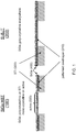
- Figs. 1-6 show various stages in a single streamlined manufacturing process that can fabricate both a SiGe-based HBT (heterojunction bipolar transistor) and a Si-based BJT (bipolar junction transistor), in accordance with some embodiments of the invention.
- SiGe-based HBT heterojunction bipolar transistor
- Si-based BJT bipolar junction transistor
- Both the SiGe HBT (heterojunction bipolar transistor) and the Si BJT (bipolar junction transistor) have their individual strengths, so integrating both types of transistors in a single integrated circuit can be advantageous to fully utilizing their individual strengths.
- integrating both a SiGe-based HBT and a Si-based BJT in the same technology can be complicated, so there is a need to develop such a single manufacturing process (which integrates both a SiGe-based HBT and a Si-based BJT) without adding a lot of process complexity.
- such an integrated circuit can include a SiGe HBT architecture consisting of a non-selectively grown SiGe base-stack, with a double-poly architecture, which deploys an implanted base Si-BJT, on top.
- the base-polysilicon layer is used to connect the SiGe intrinsic base.
- an emitter-polysilicon layer deposited in an etched emitter-window in the base-poly, forms the emitter connection.
- an implanted-base Si-BJT can be added by using a mask already present in the single manufacturing process for any device that requires a direct connection between the p+ base poly Si layer and the silicon substrate.
- the mask can be for a variable capacitor diode.
- the mask can be for a variable capacitor diode for an ESD (electrostatic discharge) clamp circuit.
- the emitter-window etch through the base-poly is shared, stopping on the SiGe base in the HBT and on the collector epi in the BJT.
- one [non-critical] implantation mask needs to be added, to implant the base of the Si-BJT through the emitter-window, while protecting the emitter-window of the SiGe-HBT.
- the emitter-poly is again shared between BJT and HBT.
- some of the transistors can be designed to use BJT, instead of HBT.
- BJT collector-to-emitter leakage
- Such an integrated circuit will have less ICEO-leakage (i.e., collector-to-emitter leakage), because the BJT does not suffer from (epitaxial) crystal defects due to a strained SiGe base present in the HBT. This in turn can result in lower, or no, yield-loss.
- such a single streamlined manufacturing process can be used to manufacture an integrated circuit device for an ESD (electrostatic discharge) clamp circuit.
- the ESD (electrostatic discharge) clamp circuit can be an ESD (electrostatic discharge) crowbar circuit.
- the integrated circuit device can be a power stage in an ESD (electrostatic discharge) crowbar circuit.
- the integrated circuit device can be a Darlington NPN bipolar power stage in an ESD (electrostatic discharge) crowbar circuit.
- such an ESD clamp circuit with a [NPN] bipolar output-stage can handle high voltages and drain high current-levels.
- the circuit can also potentially suffer from enhanced collector-to-emitter leakage (ICEO-leakage) due to crystal defects in the strained SiGe layer.
- ICEO-leakage does not need to result in yield-loss, because transistors can be switched off actively with the correct biasing.
- the transistor In an ESD-clamp, the transistor needs to be biased close to on-stage, to respond quickly in case of an ESD event. Hence, ICEO-leakage in the ESD-clamp may result in yield-loss due to unacceptably high off-state leakage current.
- the SiGe HBT is introduced for its superior RF (radio frequency) performance, but the higher frequency performance does not have any benefits for the ESD protection, and is therefore not needed.
- RF radio frequency
- An ESD clamp is provided as an example of such a device, but it should be obvious that many other devices can also benefit from the lower leakage advantage, when the higher RF performance is not required.
- a single streamlined manufacturing process that can be used for fabrication of both a SiGe-based HBT and a Si-based BJT
- Figs. 1-6 shows the implementation of such a single streamlined manufacturing process that can fabricate both a SiGe-based HBT (100) and a Si-based BJT (200), in accordance with some embodiments of the invention.
- the formation of both transistors are shown in a side-to-side cross-section view (i.e., a SiGe-based HBT (100) is shown on the left side and a Si-based BJT (200) is shown on the right side).
- Fig. 1 shows that STI (shallow trench isolation) (300) can be applied as the isolation technology for a Si substrate. It is not shown in Fig. 1 , but, in some embodiments, LOCOS (LOCal Oxidation of Silicon) can also be applied as the isolation technology for the Si substrate.
- STI shallow trench isolation
- LOCOS LOCal Oxidation of Silicon
- Fig. 1 also shows that a patterned seed-layer (310) can be deposited over all regions of a silicon substrate except for regions associated with the SiGe-based HBT.
- the patterned seed-layer (310) can be used to define the active region (320) of the SiGe HBT (i.e., by not depositing the seed-layer in the active region (320) of the SiGe HBT, or by etching away the seed-layer from the active region (320) of the SiGe HBT).
- the patterned seed-layer (310) can be comprising of one or more of the following: (a) silicon dioxide, (b) silicon nitride, and (c) undoped poly Si.
- the silicon dioxide can be LPCVD (low pressure chemical vapor deposition) Si dioxide.
- the patterned seed-layer (310) can be 50 nm thick.
- Fig. 1 further shows that a SiGe base layer (400) is deposited over all regions of the Si substrate.
- the SiGe layer (400) is poly-crystalline over all regions associated with the Si-BJT.
- the SiGe layer (400) is poly-crystalline over regions on STI and mono-crystalline over active regions (320). Therefore, the SiGe base layer (400) is poly-crystalline over all regions of the silicon substrate except the SiGe base layer (400) is mono-crystalline over the regions associated with the SiGe-based HBT (i.e., the active region of the SiGe HBT).
- the patterned seed-layer (310) causes the SiGe layer (400) to become poly-crystalline. The absence of the seed-layer over the active region of the Si HBT can cause the SiGe layer to become mono-crystalline.
- the SiGe base layer (400) is comprising of one or more of the following: (a) SiGe alloy of the form Si(1-X)Ge(X), (b) Si together with SiGe alloy of the form Si(1-X)Ge(X), (c) a 3-layer structure ofSi/Si(1-X)Ge(X)/Si, (d) a 3-layer structure of undoped Si/Si(1-X)Ge(X)/p-Si.
- p-Si can represent p-doped Si.
- the SiGe base layer (400) is shown as a 3-layer structure.
- the 3-layer structure shown in Fig. 1-6 can be (a) a 3-layer structure of Si/Si(1-X)Ge(X)/Si, or (b) a 3-layer structure of undoped Si/Si(1-X)Ge(X)/p-Si.
- Fig. 2 shows that a single streamlined manufacturing process can remove the SiGe base layer (400) over regions of the silicon substrate associated with the Si-based BJT.
- this step of removing the SiGe base layer [locally] prior to deposition of the base-poly enables for the addition of an implanted-base Si-BJT.
- this step of removing the SiGe base layer (400) can include the use of a mask already present in the single manufacturing process for any device that requires a direct connection between the p+ base poly Si layer and the silicon substrate.
- the mask can be for a variable capacitor diode.
- the mask can be for a variable capacitor diode for an ESD (electrostatic discharge) clamp circuit.
- Fig. 3 shows that, subsequent to the SiGe removal step of Fig. 2 , a poly Si layer (500) can be deposited over all regions of the silicon substrate.
- this poly Si layer (500) can be either in-situ p+ doped or doped p+ by means of implantation.
- an isolated dielectric layer (340) can be deposited over all regions of the silicon substrate.
- the isolated dielectric layer (340) can be comprising of one or more of the following: (a) LPCVD (low pressure chemical vapor deposition) silicon dioxide, (b) silicon dioxide, (c) silicon nitride.
- the isolated dielectric layer can be made up of LPCVD (low pressure chemical vapor deposition) silicon dioxide, or silicon dioxide deposited by other means, or silicon nitride, or any combination of these three materials, or any structural combination of these three materials (e.g., two layers of LPCVD dioxide plus one layer of silicon nitride sandwiched in between).
- LPCVD low pressure chemical vapor deposition
- Fig. 3 also shows that, in some embodiments, an etch-protect (or etch-stop) layer (330) can be formed between the SiGe base layer (400) and the p+ poly Si layer (500) over the regions associated with the SiGe-based HBT.
- the etch-protect layer (330) can be formed between the SiGe base layer (400) and the p+ poly Si layer (500) over the regions associated with the active regions of the SiGe-based HBT.
- the purpose of the etch-protect layer (330) is protect the SiGe layer (400) from being etched away by the p+ poly Si etch.
- the etch-protect layer (330) can be LPCVD (low pressure chemical vapor deposition) silicon dioxide. It is not shown in Fig. 3 , but, in some embodiments, it can be possible to not have the etch-protect layer (330) (i.e., skip the formation of the etch-protect layer (330)).
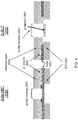
- Fig. 4 shows that a single streamlined manufacturing process can include a step of etching emitter window(s) (350) (over both SiGe HBT (100) and Si-BJT (200)).
- etching emitter window(s) (350) there can be a step of implanting base doping and optionally local collector doping in emitter window(s) over regions of the silicon substrate associated with the Si-based BJT, wherein a mask can protect emitter window(s) from implant over regions of the silicon substrate associated with the SiGe-based HBT.
- the Si-BJT will receive the implant, while the SiGe HBT will be protected from the implant by a mask.
- the step of implant is shown in Fig. 4 as a p-doped implant (360).
- Fig. 5 shows that there is a step of annealing the silicon substrate to diffuse p-doping from the p+ poly Si layer to layers below the p+ poly Si layer, wherein the p-doping from the p+ poly Si layer is diffused to the SiGe base layer for the regions associated with the SiGe-based HBT, wherein the p-doping from the p+ poly Si layer is diffused to the silicon substrate for the regions associated with the Si-based BJT.
- the p-doping from the p+ poly Si layer is diffused to the SiGe base layer below the p+ poly layer.
- the p-doping from the p+ poly Si layer is diffused to the silicon substrate directly below the p+ poly Si layer.
- the anneal will also diffuse the p-doping from p-doped implant (360) of Fig. 4 (which was implanted to the Si substrate regions exposed from the emitter window(s) etch).
- Fig. 5 also shows a step of forming an inside spacer (370) to isolate between an emitter n+ poly Si layer (520) and the p+ poly Si layer (500). Note that the emitter n+ poly Si layer (520) is not shown in Fig. 5 , because it has not yet been deposited. The emitter n+ poly Si layer (520) will be formed inside the emitter window(s) (350) for both the SiGe HBT and the Si-BJT.
- the inside spacer (370) can be a LPCVD (low pressure chemical vapor deposition) dielectric.
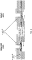
- Fig. 6 shows that there is a step of depositing and etching the emitter n+ poly Si layer (520).
- this poly Si layer (520) can be either in-situ n+ doped or doped n+ by means of implantation.
- the inside spacer (370) can isolate the emitter n+ poly Si layer (520) from the p+ poly Si layer (500).
- Fig. 6 also shows that there is a step of annealing the silicon substrate to diffuse n-doping from the emitter n+ poly Si layer into the base to form an emitter-base junction for both the SiGe-based HBT and the Si-based BJT.
- the emitter-base junction is formed by diffusing n-doping from the emitter n+ poly Si layer (520) into the SiGe base layer that is below the emitter window(s) (350). Therefore, for the SiGe-based HBT, the emitter (610) is formed by the n-doping from the emitter n+ poly Si layer (520) diffusing into the SiGe base layer.
- the base (620) is formed by the p-doped SiGe base layer.
- the collector (630) is formed by the n-doped Si substrate below the emitter window(s) (350).
- the emitter-base junction is formed by diffusing n-doping from the emitter n+ poly Si layer (520) into the Si substrate that is below the emitter window(s) (350). Therefore, for the Si-based BJT, the emitter (610) is formed by the n-doping from the emitter n+ poly Si layer (520) diffusing into the Si substrate base layer.
- the base (620) is formed by the Si substrate base layer.
- the collector (630) is formed by the n-doped Si substrate below the emitter window(s) (350).
- a buried layer n+ Si can also be formed.
- a device manufactured using a single streamlined manufacturing process can have a lower emitter-to-collector leakage due to replacement of SiGe-based HBT with Si-based BJT, wherein the Si-based BJT has a lower emitter-to-collector leakage in the device due to elimination of the SiGe base layer which has a high density of crystal defects that cause emitter-to-collector leakage.
- the device manufactured using a single streamlined manufacturing process can have a lower RF (radio frequency) performance due to the replacement of SiGe-based HBT with Si-based BJT.
- the lower RF performance is not relevant for an intended use of the device, so replacement of SiGe-based HBT with Si-based BJT can be still done to enjoy the benefit of a lower emitter-to-collector leakage due to replacement of SiGe-based HBT with Si-based BJT. This in turn can result in lower, or no, yield-loss, due to the lower emitter-to-collector leakage.
- the single streamlined manufacturing process (for example, as shown by Figs. 1-6 ) can be a BiCMOS process, so that CMOS transistors can also be included in the integrated circuit device produced using the single streamlined manufacturing process.
- the device produced using the single streamlined manufacturing process can be an ESD (electrostatic discharge) clamp circuit.
- the device produced using the single streamlined manufacturing process can be a power stage in an ESD (electrostatic discharge) crowbar circuit.
- the single streamlined manufacturing process (for example, as shown by Figs. 1-6 ) can fabricate NPN SiGe-based HBT and NPN Si-based BJT. In some embodiments, the single streamlined manufacturing process (for example, as shown by Figs. 1-6 ) can be modified to produce PNP SiGe-based HBT and PNP Si-based BJT.
- polarity of the SiGe-based HBT and the Si-based BJT devices is reversed from NPN to PNP, wherein the n-doping is replaced by p-doping and the p-doping is replaced by n-doping, wherein the n+ poly Si is replaced by p+ poly Si and the p+ poly Si is replaced by n+ poly Si.
- the present invention also provides for an integrated circuit having a substrate that includes SiGe-based HBTs (heterojunction bipolar transistors) and Si-based BJTs (bipolar junction transistors).
- the SiGe-based HBT includes: (a) a HBT collector region formed in a HBT active region in between adjacent insulation regions in the substrate, (b) a SiGe base layer stacked over the HBT active region, and (c) a HBT emitter stacked over the SiGe base layer.
- the Si-based BJT includes: (a) a BJT collector region formed in a BJT active region in between adjacent insulation regions in the substrate, (b) a Si base layer formed in the BJT active region over the collector region, and (c) a BJT emitter stacked over the Si base layer.
- the HBT collector region and the BJT collector region are formed in the same Si substrate.
- the SiGe base layer and the Si base layer are connected to a common p+ poly Si layer, wherein the common p+ poly Si layer is patterned and etched to form electrical connections of a circuit.
- the HBT emitter and the BJT emitter are formed from a common n+ poly Si layer, wherein the common n+ poly Si layer is patterned and etched to form further electrical connections of the circuit.
- this integrated circuit can be manufactured using the single streamlined manufacturing process (as shown by Figs. 1-6 ). In some embodiments, this integrated circuit can be manufactured using some other single streamlined manufacturing process.
- this integrated circuit can have a lower emitter-to-collector leakage due to replacement of SiGe-based HBT with Si-based BJT, wherein the Si-based BJT has a lower emitter-to-collector leakage in the integrated circuit due to elimination of the SiGe base layer which has a high density of crystal defects that cause emitter-to-collector leakage.
- this integrated circuit can have a lower RF (radio frequency) performance due to the replacement of SiGe-based HBT with Si-based BJT, wherein the lower RF performance is not relevant for an intended use of the integrated circuit.
- the substrate of this integrated circuit can further include CMOS (complementary metal-oxide-semiconductor) transistors. Therefore, in some embodiments, this integrated circuit can be manufactured using a single streamlined BiCMOS manufacturing process.
- CMOS complementary metal-oxide-semiconductor
- this integrated circuit can include a Darlington NPN bipolar power stage in an ESD (electrostatic discharge) crowbar circuit.
- the present invention further provides for a method comprising: (a) a npn SiGe-based HBT (heterojunction bipolar transistor) manufacturing process; (b) integrating a npn Si-based BJT (bipolar junction transistor) manufacturing process to the npn SiGe-based HBT manufacturing process. Therefore, one can take an established npn SiGe-based HBT (heterojunction bipolar transistor) manufacturing process, and then make a few modifications to also enable manufacturing of a npn Si-based BJT (bipolar junction transistor). An example of such a manufacturing process is shown by Figs. 1-6 .
- integrating the npn Si-based BJT (bipolar junction transistor) manufacturing process to the npn SiGe-based HBT manufacturing process can include: (i) re-using a base poly Si layer and an emitter poly Si layer from the npn SiGe-based HBT manufacturing process, (ii) adding one extra implant mask.
- Fig. 7A and 7B together show a process flow diagram of a method 700 for integrating a SiGe-based HBT (heterojunction bipolar transistor) and a Si-based BJT (bipolar junction transistor) together in a single manufacturing process, in accordance with some embodiments of the invention.
- the method 700 begins at step 705, where the method forms a patterned seed layer over all regions of a silicon substrate except for regions associated with the SiGe-based HBT. Then, the method proceeds to step 710.
- step 710 the method deposits a SiGe base layer over all regions of the silicon substrate, wherein the SiGe base layer is poly-crystalline over all regions of the silicon substrate except the SiGe base layer is mono-crystalline over the regions associated with the SiGe-based HBT.
- step 715 the method removes the SiGe base layer over regions of the silicon substrate associated with the Si-based BJT.
- step 720 the method deposits a poly Si layer over all regions of the silicon substrate, wherein the poly Si layer is either in-situ p+ doped or doped p+ by means of implantation.
- step 725 where the method deposits an isolated dielectric layer over all regions of the silicon substrate.
- step 730 the method etches emitter window(s).
- the method implants base doping and optionally local collector doping in emitter window(s) over regions of the silicon substrate associated with the Si-based BJT, wherein a mask protects emitter window(s) over regions of the silicon substrate associated with the SiGe-based HBT. Continuing, the method proceeds to step 740.
- step 740 the method anneals the silicon substrate to diffuse p-doping from the p+ poly Si layer to layers below the p+ poly Si layer, wherein the p-doping from the p+ poly Si layer is diffused to the SiGe base layer for the regions associated with the SiGe-based HBT, wherein the p-doping from the p+ poly Si layer is diffused to the silicon substrate for the regions associated with the Si-based BJT.
- step 745 the method forms inside spacer to isolate between an emitter n+ poly Si layer and the p+ poly Si layer. Continuing to step 750, the method deposits and etches the emitter n+ poly Si layer.
- step 755 the method anneals the silicon substrate to diffuse n-doping from the emitter n+ poly Si layer into the base to form an emitter-base junction for both the SiGe-based HBT and the Si-based BJT.
- This specification discloses methods for integrating a SiGe-based HBT (heterojunction bipolar transistor) and a Si-based BJT (bipolar junction transistor) together in a single manufacturing process that does not add a lot of process complexity, and an integrated circuit that can be fabricated utilizing such a streamlined manufacturing process.
- such an integrated circuit can enjoy both the benefits of a higher RF (radio frequency) performance for the SiGe HBT and a lower leakage current for the Si-based BJT.
- such an integrated circuit can be applied to an ESD (electrostatic discharge) clamp circuit, in order to achieve a lower, or no, yield-loss.
Landscapes
- Chemical & Material Sciences (AREA)
- Bipolar Transistors (AREA)
- Bipolar Integrated Circuits (AREA)
- Chemical Kinetics & Catalysis (AREA)
- General Chemical & Material Sciences (AREA)
- Crystallography & Structural Chemistry (AREA)
Abstract
Description
- The described embodiments relate generally to methods and devices related to the manufacturing and use of a SiGe HBT (silicon-germanium heterojunction bipolar transistor), and more particularly to methods and devices related to the manufacturing and use of a Si BJT (silicon bipolar junction transistor) integrated together with a SiGe HBT.
- Both the SiGe HBT (heterojunction bipolar transistor) and the Si BJT (bipolar junction transistor) have their individual strengths, so it can be advantageous to integrate both types of transistors in a single integrated circuit in order to fully utilize their individual strengths. However, in general, it is not straightforward to integrate both a SiGe-based HBT and a Si-based BJT in the same technology, without adding a lot of process complexity.
- Therefore, there are strong motivations to develop a single manufacturing process that can integrate both a SiGe-based HBT and a Si-based BJT, without adding a lot of process complexity.
- This specification discloses methods for integrating a SiGe-based HBT (heterojunction bipolar transistor) and a Si-based BJT (bipolar junction transistor) together in a single manufacturing process that does not add a lot of process complexity, and an integrated circuit that can be fabricated utilizing such a streamlined manufacturing process. In some embodiments, such an integrated circuit can enjoy both the benefits of a higher RF (radio frequency) performance for the SiGe HBT and a lower leakage current for the Si-based BJT. In some embodiments, such an integrated circuit can be applied to an ESD (electrostatic discharge) clamp circuit, in order to achieve a lower, or no, yield-loss.
- In summary, for some embodiments of such a streamlined manufacturing process, with the addition of one extra [non-critical] implant mask, and re-using the base-polysilicon and emitter-polysilicon layers from the SiGe HBT, an implanted-base Si-BJT can be created. Since the SiGe layer, with potentially a high density of crystal-defects, is removed from the Si-BJT, unwanted [emitter-to-collector] leakage in this device due to crystal defects is thereby eliminated. As an example, the power-stage in an ESD clamp (e.g., crowbar circuit) is usually large, resulting in high yield-loss when applying a SiGe HBT. The Si-BJT (replacing the SiGe HBT) will have a [much] lower RF-performance, e.g. lower fT, but for the intended use-case in the power-stage in an ESD Clamp, this is not relevant.
- In some embodiments such a streamlined manufacturing process can be created by combining an implanted-base NPN Si-BJT with a epitaxially grown SiGe-base HBT in the same technology, re-using the extrinsic base connection and poly-emitter for both, without adding complexity.
- The present invention provides for a method for integrating a SiGe-based HBT (heterojunction bipolar transistor) and a Si-based BJT (bipolar junction transistor) in a single manufacturing process, the method comprising: (a) forming a patterned seed layer over all regions of a silicon substrate except for regions associated with the SiGe-based HBT; (b) depositing a SiGe base layer over all regions of the silicon substrate, wherein the SiGe base layer is poly-crystalline over all regions of the silicon substrate except the SiGe base layer is mono-crystalline over the regions associated with the SiGe-based HBT; (c) removing the SiGe base layer over regions of the silicon substrate associated with the Si-based BJT; (d) depositing a poly Si layer over all regions of the silicon substrate, wherein the poly Si layer is either in-situ p+ doped or doped p+ by means of implantation; (e) depositing an isolated dielectric layer over all regions of the silicon substrate; (f) etching emitter window(s); (g) implanting base doping and optionally local collector doping in emitter window(s) over regions of the silicon substrate associated with the Si-based BJT, wherein a mask protects emitter window(s) over regions of the silicon substrate associated with the SiGe-based HBT; (h) annealing the silicon substrate to diffuse p-doping from the p+ poly Si layer to layers below the p+ poly Si layer, wherein the p-doping from the p+ poly Si layer is diffused to the SiGe base layer for the regions associated with the SiGe-based HBT, wherein the p-doping from the p+ poly Si layer is diffused to the silicon substrate for the regions associated with the Si-based BJT; (i) forming inside spacer to isolate between an emitter n+ poly Si layer and the p+ poly Si layer; (j) depositing and etching the emitter n+ poly Si layer; (k) annealing the silicon substrate to diffuse n-doping from the emitter n+ poly Si layer into the base to form an emitter-base junction for both the SiGe-based HBT and the Si-based BJT.
- In some embodiments, a device manufactured using the method has a lower emitter-to-collector leakage due to replacement of SiGe-based HBT with Si-based BJT, wherein the Si-based BJT has a lower emitter-to-collector leakage in the device due to elimination of the SiGe base layer which has a high density of crystal defects that cause emitter-to-collector leakage.
- In some embodiments, the device manufactured using the method has a lower RF (radio frequency) performance due to the replacement of SiGe-based HBT with Si-based BJT, wherein the lower RF performance is not relevant for an intended use of the device.
- In some embodiments, the single manufacturing process is a BiCMOS process.
- In some embodiments, the device is an ESD (electrostatic discharge) clamp circuit.
- In some embodiments, the device is a power stage in an ESD (electrostatic discharge) crowbar circuit.
- In some embodiments, the step of removing the SiGe base layer over regions of the silicon substrate associated with the Si-based BJT comprises use of a mask already present in the single manufacturing process for any device that requires a direct connection between the p+ base poly Si layer and the silicon substrate.
- In some embodiments, polarity of the SiGe-based HBT and the Si-based BJT devices is reversed from NPN to PNP, wherein the n-doping is replaced by p-doping and the p-doping is replaced by n-doping, wherein the n+ poly Si is replaced by p+ poly Si and the p+ poly Si is replaced by n+ poly Si.
- In some embodiments, the patterned seed layer is comprising of one or more of the following: (i) silicon dioxide, (ii) silicon nitride, (iii) undoped poly Si.
- In some embodiments, the SiGe base layer is comprising of one or more of the following: (i) SiGe alloy of the form Si(1-X)Ge(X), (ii) Si together with SiGe alloy of the form Si(1-X)Ge(X), (iii) a 3-layer structure of Si/Si(1-X)Ge(X)/Si, (iv) a 3-layer structure of undoped Si/Si(1-X)Ge(X)/p-Si.
- In some embodiments, the isolated dielectric layer is comprising of one or more of the following: (i) LPCVD (low pressure chemical vapor deposition) silicon dioxide, (ii) silicon dioxide, (iii) silicon nitride.
- In some embodiments, the method further comprising: (1) forming an etch-protect layer between the SiGe base layer and the p+ poly Si layer over the regions associated with the SiGe-based HBT.
- In some embodiments, the etch-protect layer is LPCVD (low pressure chemical vapor deposition) silicon dioxide.
- The present invention also provides for an integrated circuit having a substrate comprising a plurality of bipolar transistors including a SiGe-based HBT (heterojunction bipolar transistor) and a Si-based BJT (bipolar junction transistor); (a) the SiGe-based HBT comprising a HBT collector region formed in a HBT active region in between adjacent insulation regions in the substrate, a SiGe base layer stacked over the HBT active region, and a HBT emitter stacked over the SiGe base layer, and (b) the Si-based BJT comprising a BJT collector region formed in a BJT active region in between adjacent insulation regions in the substrate, a Si base layer formed in the BJT active region over the collector region, and a BJT emitter stacked over the Si base layer, (c) wherein the HBT collector region and the BJT collector region are formed in the same Si substrate, (d) wherein the SiGe base layer and the Si base layer are connected to a common p+ poly Si layer, wherein the common p+ poly Si layer is patterned and etched to form electrical connections of a circuit, (e) wherein the HBT emitter and the BJT emitter are formed from a common n+ poly Si layer, wherein the common n+ poly Si layer is patterned and etched to form further electrical connections of the circuit.
- In some embodiments, the integrated circuit has a lower emitter-to-collector leakage due to replacement of SiGe-based HBT with Si-based BJT, wherein the Si-based BJT has a lower emitter-to-collector leakage in the integrated circuit due to elimination of the SiGe base layer which has a high density of crystal defects that cause emitter-to-collector leakage.
- In some embodiments, the integrated circuit has a lower RF (radio frequency) performance due to the replacement of SiGe-based HBT with Si-based BJT, wherein the lower RF performance is not relevant for an intended use of the integrated circuit.
- In some embodiments, the substrate further comprising CMOS (complementary metal-oxide-semiconductor) transistors.
- In some embodiments, the integrated circuit comprises a Darlington NPN bipolar power stage in an ESD (electrostatic discharge) crowbar circuit.
- The present invention further provides for a method comprising: (a) a npn SiGe-based HBT (heterojunction bipolar transistor) manufacturing process; (b) integrating a npn Si-based BJT (bipolar junction transistor) manufacturing process to the npn SiGe-based HBT manufacturing process.
- In some embodiments, integrating the npn Si-based BJT (bipolar junction transistor) manufacturing process to the npn SiGe-based HBT manufacturing process comprises: (i) re-using a base poly Si layer and an emitter poly Si layer from the npn SiGe-based HBT manufacturing process, (ii) adding one extra implant mask.
- The above summary is not intended to represent every example embodiment within the scope of the current or future Claim sets. Additional example embodiments are discussed within the Figures and Detailed Description below. Other aspects and advantages of embodiments of the present invention will become apparent from the following detailed description taken in conjunction with the accompanying drawings.
- In general,
Figs. 1-6 show various stages in a single streamlined manufacturing process that can fabricate both a SiGe-based HBT (heterojunction bipolar transistor) and a Si-based BJT (bipolar junction transistor), in accordance with some embodiments of the invention. - In detail,
Fig. 1 shows formation of a patterned seed layer and deposition of a SiGe base layer, in accordance with some embodiments of the invention. -
Fig. 2 shows removal of the SiGe base layer over Si-based BJT regions, in accordance with some embodiments of the invention. -
Fig. 3 shows deposition of a poly Si layer and an isolated dielectric layer, in accordance with some embodiments of the invention. -
Fig. 4 shows etch of emitter window(s) and implant of base doping, in accordance with some embodiments of the invention. -
Fig. 5 shows anneal of the silicon substrate to diffuse p-doping from the p+ poly Si layer and formation of inside spacer, in accordance with some embodiments of the invention. -
Fig. 6 shows deposition and etch of the emitter n+ poly Si layer, together with anneal of the silicon substrate to form an emitter-base junction, in accordance with some embodiments of the invention. -
Fig. 7A and7B together show a process flow diagram of a method for integrating a SiGe-based HBT (heterojunction bipolar transistor) and a Si-based BJT (bipolar junction transistor) together in a single manufacturing process, in accordance with some embodiments of the invention. - It will be readily understood that the steps and components of the embodiments as generally described herein and illustrated in the appended figures could be arranged and designed in a wide variety of different order and configurations. Thus, the following more detailed description of various embodiments, as represented in the figures, is not intended to limit the scope of the present disclosure, but is merely representative of various embodiments. While the various aspects of the embodiments are presented in drawings, the drawings are not necessarily drawn to scale unless specifically indicated.
- The present invention may be embodied in other specific forms without departing from its spirit or essential characteristics. The described embodiments are to be considered in all respects only as illustrative and not restrictive. The scope of the invention is, therefore, indicated by the appended claims rather than by this detailed description. All changes which come within the meaning and range of equivalency of the claims are to be embraced within their scope.
- Reference throughout this specification to features, advantages, or similar language does not imply that all of the features and advantages that may be realized with the present invention should be or are in any single embodiment of the invention. Rather, language referring to the features and advantages is understood to mean that a specific feature, advantage, or characteristic described in connection with an embodiment is included in at least one embodiment of the present invention. Thus, discussions of the features and advantages, and similar language, throughout this specification may, but do not necessarily, refer to the same embodiment.
- Furthermore, the described features, advantages, and characteristics of the invention may be combined in any suitable manner in one or more embodiments. One skilled in the relevant art will recognize, in light of the description herein, that the invention can be practiced without one or more of the specific features or advantages of a particular embodiment. In other instances, additional features and advantages may be recognized in certain embodiments that may not be present in all embodiments of the invention.
- Both the SiGe HBT (heterojunction bipolar transistor) and the Si BJT (bipolar junction transistor) have their individual strengths, so integrating both types of transistors in a single integrated circuit can be advantageous to fully utilizing their individual strengths. However, integrating both a SiGe-based HBT and a Si-based BJT in the same technology can be complicated, so there is a need to develop such a single manufacturing process (which integrates both a SiGe-based HBT and a Si-based BJT) without adding a lot of process complexity.
- This specification discloses methods for implementing such a single streamlined manufacturing process, and an integrated circuit that can be fabricated by such a streamlined manufacturing process. In some embodiments, such an integrated circuit can include a SiGe HBT architecture consisting of a non-selectively grown SiGe base-stack, with a double-poly architecture, which deploys an implanted base Si-BJT, on top.
- In some embodiments, for such an integrated circuit, the base-polysilicon layer is used to connect the SiGe intrinsic base.
- In some embodiments, for such an integrated circuit, an emitter-polysilicon layer, deposited in an etched emitter-window in the base-poly, forms the emitter connection.
- In some embodiments, for such an integrated circuit, by removing the SiGe layer [locally] prior to deposition of the base-poly, an implanted-base Si-BJT can be added by using a mask already present in the single manufacturing process for any device that requires a direct connection between the p+ base poly Si layer and the silicon substrate. As an example, in some embodiments, the mask can be for a variable capacitor diode. As a further example, in some embodiments, the mask can be for a variable capacitor diode for an ESD (electrostatic discharge) clamp circuit.
- In some embodiments, for such an integrated circuit, the emitter-window etch through the base-poly is shared, stopping on the SiGe base in the HBT and on the collector epi in the BJT.
- In some embodiments, for such an integrated circuit, one [non-critical] implantation mask needs to be added, to implant the base of the Si-BJT through the emitter-window, while protecting the emitter-window of the SiGe-HBT.
- In some embodiments, for such an integrated circuit, the emitter-poly is again shared between BJT and HBT.
- In some embodiments, for such an integrated circuit, some of the transistors can be designed to use BJT, instead of HBT. Such an integrated circuit will have less ICEO-leakage (i.e., collector-to-emitter leakage), because the BJT does not suffer from (epitaxial) crystal defects due to a strained SiGe base present in the HBT. This in turn can result in lower, or no, yield-loss.
- As an example, in some embodiments, such a single streamlined manufacturing process can be used to manufacture an integrated circuit device for an ESD (electrostatic discharge) clamp circuit. In some embodiments, the ESD (electrostatic discharge) clamp circuit can be an ESD (electrostatic discharge) crowbar circuit. In some embodiments, the integrated circuit device can be a power stage in an ESD (electrostatic discharge) crowbar circuit. In some embodiments, the integrated circuit device can be a Darlington NPN bipolar power stage in an ESD (electrostatic discharge) crowbar circuit.
- In some embodiments, such an ESD clamp circuit with a [NPN] bipolar output-stage can handle high voltages and drain high current-levels. However, when implementing in an advanced SiGe-HBT BiCMOS process, the circuit can also potentially suffer from enhanced collector-to-emitter leakage (ICEO-leakage) due to crystal defects in the strained SiGe layer. In active circuitry, this ICEO-leakage does not need to result in yield-loss, because transistors can be switched off actively with the correct biasing.
- In an ESD-clamp, the transistor needs to be biased close to on-stage, to respond quickly in case of an ESD event. Hence, ICEO-leakage in the ESD-clamp may result in yield-loss due to unacceptably high off-state leakage current.
- The SiGe HBT is introduced for its superior RF (radio frequency) performance, but the higher frequency performance does not have any benefits for the ESD protection, and is therefore not needed. Hence, there are clear advantages to implementing a single streamlined manufacturing process that can produce both a SiGe-based HBT and a Si-based BJT, after adding minimal additional complexity to the manufacturing process. It is also clear that such a process can be effectively applied to devices or parts of devices that do not require the higher RF (radio frequency) performance of the HBT, so that the HBT components can be replaced by the lower leakage BJT components. An ESD clamp is provided as an example of such a device, but it should be obvious that many other devices can also benefit from the lower leakage advantage, when the higher RF performance is not required. In other words, such a single streamlined manufacturing process (that can be used for fabrication of both a SiGe-based HBT and a Si-based BJT) can be effectively applied to any devices or parts of devices that can benefit from both the higher RF performance of a SiGe-based HBT and the lower leakage current of a Si-based BJT.
-
Figs. 1-6 shows the implementation of such a single streamlined manufacturing process that can fabricate both a SiGe-based HBT (100) and a Si-based BJT (200), in accordance with some embodiments of the invention. InFigs. 1-6 , the formation of both transistors are shown in a side-to-side cross-section view (i.e., a SiGe-based HBT (100) is shown on the left side and a Si-based BJT (200) is shown on the right side). -
Fig. 1 shows that STI (shallow trench isolation) (300) can be applied as the isolation technology for a Si substrate. It is not shown inFig. 1 , but, in some embodiments, LOCOS (LOCal Oxidation of Silicon) can also be applied as the isolation technology for the Si substrate. -
Fig. 1 also shows that a patterned seed-layer (310) can be deposited over all regions of a silicon substrate except for regions associated with the SiGe-based HBT. In some embodiments, the patterned seed-layer (310) can be used to define the active region (320) of the SiGe HBT (i.e., by not depositing the seed-layer in the active region (320) of the SiGe HBT, or by etching away the seed-layer from the active region (320) of the SiGe HBT). In some embodiments, the patterned seed-layer (310) can be comprising of one or more of the following: (a) silicon dioxide, (b) silicon nitride, and (c) undoped poly Si. In some embodiments, the silicon dioxide can be LPCVD (low pressure chemical vapor deposition) Si dioxide. In some embodiments, the patterned seed-layer (310) can be 50 nm thick. -
Fig. 1 further shows that a SiGe base layer (400) is deposited over all regions of the Si substrate. The SiGe layer (400) is poly-crystalline over all regions associated with the Si-BJT. For the regions associated with the SiGe HBT, the SiGe layer (400) is poly-crystalline over regions on STI and mono-crystalline over active regions (320). Therefore, the SiGe base layer (400) is poly-crystalline over all regions of the silicon substrate except the SiGe base layer (400) is mono-crystalline over the regions associated with the SiGe-based HBT (i.e., the active region of the SiGe HBT). The patterned seed-layer (310) causes the SiGe layer (400) to become poly-crystalline. The absence of the seed-layer over the active region of the Si HBT can cause the SiGe layer to become mono-crystalline. - In some embodiments, the SiGe base layer (400) is comprising of one or more of the following: (a) SiGe alloy of the form Si(1-X)Ge(X), (b) Si together with SiGe alloy of the form Si(1-X)Ge(X), (c) a 3-layer structure ofSi/Si(1-X)Ge(X)/Si, (d) a 3-layer structure of undoped Si/Si(1-X)Ge(X)/p-Si. In some embodiments, p-Si can represent p-doped Si. In
Fig. 1 (and alsoFigs. 2-6 ), the SiGe base layer (400) is shown as a 3-layer structure. In some embodiments, the 3-layer structure shown inFig. 1-6 can be (a) a 3-layer structure of Si/Si(1-X)Ge(X)/Si, or (b) a 3-layer structure of undoped Si/Si(1-X)Ge(X)/p-Si. -
Fig. 2 shows that a single streamlined manufacturing process can remove the SiGe base layer (400) over regions of the silicon substrate associated with the Si-based BJT. In some embodiments, this step of removing the SiGe base layer [locally] prior to deposition of the base-poly enables for the addition of an implanted-base Si-BJT. In some embodiments, this step of removing the SiGe base layer (400) can include the use of a mask already present in the single manufacturing process for any device that requires a direct connection between the p+ base poly Si layer and the silicon substrate. In some embodiments, the mask can be for a variable capacitor diode. In some embodiments, the mask can be for a variable capacitor diode for an ESD (electrostatic discharge) clamp circuit. -
Fig. 3 shows that, subsequent to the SiGe removal step ofFig. 2 , a poly Si layer (500) can be deposited over all regions of the silicon substrate. In some embodiment, this poly Si layer (500) can be either in-situ p+ doped or doped p+ by means of implantation. After the poly Si layer (500) has been deposited, an isolated dielectric layer (340) can be deposited over all regions of the silicon substrate. In some embodiment, the isolated dielectric layer (340) can be comprising of one or more of the following: (a) LPCVD (low pressure chemical vapor deposition) silicon dioxide, (b) silicon dioxide, (c) silicon nitride. This means that the isolated dielectric layer can be made up of LPCVD (low pressure chemical vapor deposition) silicon dioxide, or silicon dioxide deposited by other means, or silicon nitride, or any combination of these three materials, or any structural combination of these three materials (e.g., two layers of LPCVD dioxide plus one layer of silicon nitride sandwiched in between). -
Fig. 3 also shows that, in some embodiments, an etch-protect (or etch-stop) layer (330) can be formed between the SiGe base layer (400) and the p+ poly Si layer (500) over the regions associated with the SiGe-based HBT. In some embodiments, the etch-protect layer (330) can be formed between the SiGe base layer (400) and the p+ poly Si layer (500) over the regions associated with the active regions of the SiGe-based HBT. The purpose of the etch-protect layer (330) is protect the SiGe layer (400) from being etched away by the p+ poly Si etch. In some embodiments, the etch-protect layer (330) can be LPCVD (low pressure chemical vapor deposition) silicon dioxide. It is not shown inFig. 3 , but, in some embodiments, it can be possible to not have the etch-protect layer (330) (i.e., skip the formation of the etch-protect layer (330)). -
Fig. 4 shows that a single streamlined manufacturing process can include a step of etching emitter window(s) (350) (over both SiGe HBT (100) and Si-BJT (200)). Following the step of etching emitter window(s) (350), there can be a step of implanting base doping and optionally local collector doping in emitter window(s) over regions of the silicon substrate associated with the Si-based BJT, wherein a mask can protect emitter window(s) from implant over regions of the silicon substrate associated with the SiGe-based HBT. In other word, the Si-BJT will receive the implant, while the SiGe HBT will be protected from the implant by a mask. The step of implant is shown inFig. 4 as a p-doped implant (360). -
Fig. 5 shows that there is a step of annealing the silicon substrate to diffuse p-doping from the p+ poly Si layer to layers below the p+ poly Si layer, wherein the p-doping from the p+ poly Si layer is diffused to the SiGe base layer for the regions associated with the SiGe-based HBT, wherein the p-doping from the p+ poly Si layer is diffused to the silicon substrate for the regions associated with the Si-based BJT. InFig. 5 , it can be seen that for the SiGe-based HBT, the p-doping from the p+ poly Si layer is diffused to the SiGe base layer below the p+ poly layer. For the Si-based BJT, it can be seen that the p-doping from the p+ poly Si layer is diffused to the silicon substrate directly below the p+ poly Si layer. Of course, the anneal will also diffuse the p-doping from p-doped implant (360) ofFig. 4 (which was implanted to the Si substrate regions exposed from the emitter window(s) etch). - Additionally,
Fig. 5 also shows a step of forming an inside spacer (370) to isolate between an emitter n+ poly Si layer (520) and the p+ poly Si layer (500). Note that the emitter n+ poly Si layer (520) is not shown inFig. 5 , because it has not yet been deposited. The emitter n+ poly Si layer (520) will be formed inside the emitter window(s) (350) for both the SiGe HBT and the Si-BJT. In some embodiments, the inside spacer (370) can be a LPCVD (low pressure chemical vapor deposition) dielectric. -
Fig. 6 shows that there is a step of depositing and etching the emitter n+ poly Si layer (520). In some embodiment, this poly Si layer (520) can be either in-situ n+ doped or doped n+ by means of implantation. InFig. 6 , it can be seen that the inside spacer (370) can isolate the emitter n+ poly Si layer (520) from the p+ poly Si layer (500). -
Fig. 6 also shows that there is a step of annealing the silicon substrate to diffuse n-doping from the emitter n+ poly Si layer into the base to form an emitter-base junction for both the SiGe-based HBT and the Si-based BJT. InFig. 6 , it can be seen that for the SiGe-based HBT, the emitter-base junction is formed by diffusing n-doping from the emitter n+ poly Si layer (520) into the SiGe base layer that is below the emitter window(s) (350). Therefore, for the SiGe-based HBT, the emitter (610) is formed by the n-doping from the emitter n+ poly Si layer (520) diffusing into the SiGe base layer. The base (620) is formed by the p-doped SiGe base layer. The collector (630) is formed by the n-doped Si substrate below the emitter window(s) (350). - For the Si-based BJT, it can be seen that the emitter-base junction is formed by diffusing n-doping from the emitter n+ poly Si layer (520) into the Si substrate that is below the emitter window(s) (350). Therefore, for the Si-based BJT, the emitter (610) is formed by the n-doping from the emitter n+ poly Si layer (520) diffusing into the Si substrate base layer. The base (620) is formed by the Si substrate base layer. The collector (630) is formed by the n-doped Si substrate below the emitter window(s) (350).
- In some embodiments, a buried layer n+ Si can also be formed.
- In some embodiments, a device manufactured using a single streamlined manufacturing process (for example, as shown by
Figs. 1-6 ) can have a lower emitter-to-collector leakage due to replacement of SiGe-based HBT with Si-based BJT, wherein the Si-based BJT has a lower emitter-to-collector leakage in the device due to elimination of the SiGe base layer which has a high density of crystal defects that cause emitter-to-collector leakage. - In some embodiments, the device manufactured using a single streamlined manufacturing process (for example, as shown by
Figs. 1-6 ) can have a lower RF (radio frequency) performance due to the replacement of SiGe-based HBT with Si-based BJT. But the lower RF performance is not relevant for an intended use of the device, so replacement of SiGe-based HBT with Si-based BJT can be still done to enjoy the benefit of a lower emitter-to-collector leakage due to replacement of SiGe-based HBT with Si-based BJT. This in turn can result in lower, or no, yield-loss, due to the lower emitter-to-collector leakage. - In some embodiments, the single streamlined manufacturing process (for example, as shown by
Figs. 1-6 ) can be a BiCMOS process, so that CMOS transistors can also be included in the integrated circuit device produced using the single streamlined manufacturing process. - In some embodiments, the device produced using the single streamlined manufacturing process (for example, as shown by
Figs. 1-6 ) can be an ESD (electrostatic discharge) clamp circuit. - In some embodiments, the device produced using the single streamlined manufacturing process (for example, as shown by
Figs. 1-6 ) can be a power stage in an ESD (electrostatic discharge) crowbar circuit. - In some embodiments, the single streamlined manufacturing process (for example, as shown by
Figs. 1-6 ) can fabricate NPN SiGe-based HBT and NPN Si-based BJT. In some embodiments, the single streamlined manufacturing process (for example, as shown byFigs. 1-6 ) can be modified to produce PNP SiGe-based HBT and PNP Si-based BJT. Therefore, polarity of the SiGe-based HBT and the Si-based BJT devices is reversed from NPN to PNP, wherein the n-doping is replaced by p-doping and the p-doping is replaced by n-doping, wherein the n+ poly Si is replaced by p+ poly Si and the p+ poly Si is replaced by n+ poly Si. - The present invention also provides for an integrated circuit having a substrate that includes SiGe-based HBTs (heterojunction bipolar transistors) and Si-based BJTs (bipolar junction transistors). The SiGe-based HBT includes: (a) a HBT collector region formed in a HBT active region in between adjacent insulation regions in the substrate, (b) a SiGe base layer stacked over the HBT active region, and (c) a HBT emitter stacked over the SiGe base layer. The Si-based BJT includes: (a) a BJT collector region formed in a BJT active region in between adjacent insulation regions in the substrate, (b) a Si base layer formed in the BJT active region over the collector region, and (c) a BJT emitter stacked over the Si base layer. For this integrated circuit, the HBT collector region and the BJT collector region are formed in the same Si substrate. For this integrated circuit, the SiGe base layer and the Si base layer are connected to a common p+ poly Si layer, wherein the common p+ poly Si layer is patterned and etched to form electrical connections of a circuit. For this integrated circuit, the HBT emitter and the BJT emitter are formed from a common n+ poly Si layer, wherein the common n+ poly Si layer is patterned and etched to form further electrical connections of the circuit.
- In some embodiments, this integrated circuit can be manufactured using the single streamlined manufacturing process (as shown by
Figs. 1-6 ). In some embodiments, this integrated circuit can be manufactured using some other single streamlined manufacturing process. - In some embodiments, this integrated circuit can have a lower emitter-to-collector leakage due to replacement of SiGe-based HBT with Si-based BJT, wherein the Si-based BJT has a lower emitter-to-collector leakage in the integrated circuit due to elimination of the SiGe base layer which has a high density of crystal defects that cause emitter-to-collector leakage.
- In some embodiments, this integrated circuit can have a lower RF (radio frequency) performance due to the replacement of SiGe-based HBT with Si-based BJT, wherein the lower RF performance is not relevant for an intended use of the integrated circuit.
- In some embodiments, the substrate of this integrated circuit can further include CMOS (complementary metal-oxide-semiconductor) transistors. Therefore, in some embodiments, this integrated circuit can be manufactured using a single streamlined BiCMOS manufacturing process.
- In some embodiments, this integrated circuit can include a Darlington NPN bipolar power stage in an ESD (electrostatic discharge) crowbar circuit.
- The present invention further provides for a method comprising: (a) a npn SiGe-based HBT (heterojunction bipolar transistor) manufacturing process; (b) integrating a npn Si-based BJT (bipolar junction transistor) manufacturing process to the npn SiGe-based HBT manufacturing process. Therefore, one can take an established npn SiGe-based HBT (heterojunction bipolar transistor) manufacturing process, and then make a few modifications to also enable manufacturing of a npn Si-based BJT (bipolar junction transistor). An example of such a manufacturing process is shown by
Figs. 1-6 . - In some embodiments, integrating the npn Si-based BJT (bipolar junction transistor) manufacturing process to the npn SiGe-based HBT manufacturing process can include: (i) re-using a base poly Si layer and an emitter poly Si layer from the npn SiGe-based HBT manufacturing process, (ii) adding one extra implant mask.
-
Fig. 7A and7B together show a process flow diagram of amethod 700 for integrating a SiGe-based HBT (heterojunction bipolar transistor) and a Si-based BJT (bipolar junction transistor) together in a single manufacturing process, in accordance with some embodiments of the invention. As shown inFig. 7A , themethod 700 begins atstep 705, where the method forms a patterned seed layer over all regions of a silicon substrate except for regions associated with the SiGe-based HBT. Then, the method proceeds to step 710. Instep 710, the method deposits a SiGe base layer over all regions of the silicon substrate, wherein the SiGe base layer is poly-crystalline over all regions of the silicon substrate except the SiGe base layer is mono-crystalline over the regions associated with the SiGe-based HBT. Next, atstep 715, the method removes the SiGe base layer over regions of the silicon substrate associated with the Si-based BJT. Continuing to step 720, the method deposits a poly Si layer over all regions of the silicon substrate, wherein the poly Si layer is either in-situ p+ doped or doped p+ by means of implantation. Then the method proceeds to step 725, where the method deposits an isolated dielectric layer over all regions of the silicon substrate. Subsequently instep 730, the method etches emitter window(s). - Then the process continues to
Fig. 7B , and atstep 735, the method implants base doping and optionally local collector doping in emitter window(s) over regions of the silicon substrate associated with the Si-based BJT, wherein a mask protects emitter window(s) over regions of the silicon substrate associated with the SiGe-based HBT. Continuing, the method proceeds to step 740. Instep 740, the method anneals the silicon substrate to diffuse p-doping from the p+ poly Si layer to layers below the p+ poly Si layer, wherein the p-doping from the p+ poly Si layer is diffused to the SiGe base layer for the regions associated with the SiGe-based HBT, wherein the p-doping from the p+ poly Si layer is diffused to the silicon substrate for the regions associated with the Si-based BJT. Next, atstep 745, the method forms inside spacer to isolate between an emitter n+ poly Si layer and the p+ poly Si layer. Continuing to step 750, the method deposits and etches the emitter n+ poly Si layer. Finally, at step 755, the method anneals the silicon substrate to diffuse n-doping from the emitter n+ poly Si layer into the base to form an emitter-base junction for both the SiGe-based HBT and the Si-based BJT. - This specification discloses methods for integrating a SiGe-based HBT (heterojunction bipolar transistor) and a Si-based BJT (bipolar junction transistor) together in a single manufacturing process that does not add a lot of process complexity, and an integrated circuit that can be fabricated utilizing such a streamlined manufacturing process. In some embodiments, such an integrated circuit can enjoy both the benefits of a higher RF (radio frequency) performance for the SiGe HBT and a lower leakage current for the Si-based BJT. In some embodiments, such an integrated circuit can be applied to an ESD (electrostatic discharge) clamp circuit, in order to achieve a lower, or no, yield-loss.
- In this specification, example embodiments have been presented in terms of a selected set of details. However, a person of ordinary skill in the art would understand that many other example embodiments may be practiced which include a different selected set of these details. It is intended that the following claims cover all possible example embodiments.
- Although the operations of the method(s) herein are shown and described in a particular order, the order of the operations of each method may be altered so that certain operations may be performed in an inverse order or so that certain operations may be performed, at least in part, concurrently with other operations. In another embodiment, instructions or sub-operations of distinct operations may be implemented in an intermittent and/or alternating manner.
- The various aspects, embodiments, implementations or features of the described embodiments can be used separately or in any combination.
- The foregoing description, for purposes of explanation, used specific nomenclature to provide a thorough understanding of the described embodiments. However, it will be apparent to one skilled in the art that the specific details are not required in order to practice the described embodiments. Thus, the foregoing descriptions of specific embodiments are presented for purposes of illustration and description. They are not intended to be exhaustive or to limit the described embodiments to the precise forms disclosed. It will be apparent to one of ordinary skill in the art that many modifications and variations are possible in view of the above teachings.
Claims (15)
- A method for integrating a SiGe-based HBT (heterojunction bipolar transistor) and a Si-based BJT (bipolar junction transistor) in a single manufacturing process, the method comprising:forming a patterned seed layer over all regions of a silicon substrate except for regions associated with the SiGe-based HBT;depositing a SiGe base layer over all regions of the silicon substrate, wherein the SiGe base layer is poly-crystalline over all regions of the silicon substrate except the SiGe base layer is mono-crystalline over the regions associated with the SiGe-based HBT;removing the SiGe base layer over regions of the silicon substrate associated with the Si-based BJT;depositing a poly Si layer over all regions of the silicon substrate, wherein the poly Si layer is either in-situ p+ doped or doped p+ by means of implantation;depositing an isolated dielectric layer over all regions of the silicon substrate;etching emitter window(s);implanting base doping and optionally local collector doping in emitter window(s) over regions of the silicon substrate associated with the Si-based BJT, wherein a mask protects emitter window(s) over regions of the silicon substrate associated with the SiGe-based HBT;annealing the silicon substrate to diffuse p-doping from the p+ poly Si layer to layers below the p+ poly Si layer, wherein the p-doping from the p+ poly Si layer is diffused to the SiGe base layer for the regions associated with the SiGe-based HBT, wherein the p-doping from the p+ poly Si layer is diffused to the silicon substrate for the regions associated with the Si-based BJT;forming inside spacer to isolate between an emitter n+ poly Si layer and the p+ poly Si layer;depositing and etching the emitter n+ poly Si layer;annealing the silicon substrate to diffuse n-doping from the emitter n+ poly Si layer into the base to form an emitter-base junction for both the SiGe-based HBT and the Si-based BJT.
- The method of claim 1, wherein the single manufacturing process is a BiCMOS process.
- The method of any preceding claim, wherein the device is an ESD (electrostatic discharge) clamp circuit.
- The method of any preceding claim, wherein the device is a power stage in an ESD (electrostatic discharge) crowbar circuit.
- The method of any preceding claim , wherein the step of removing the SiGe base layer over regions of the silicon substrate associated with the Si-based BJT comprises use of a mask already present in the single manufacturing process for any device that requires a direct connection between the p+ base poly Si layer and the silicon substrate.
- The method of any preceding claim, wherein polarity of the SiGe-based HBT and the Si-based BJT devices is reversed from NPN to PNP, wherein the n-doping is replaced by p-doping and the p-doping is replaced by n-doping, wherein the n+ poly Si is replaced by p+ poly Si and the p+ poly Si is replaced by n+ poly Si.
- The method of any preceding claim, wherein the patterned seed layer is comprising of one or more of the following:silicon dioxide,silicon nitride,undoped poly Si.
- The method of any preceding claim, wherein the SiGe base layer is comprising of one or more of the following:SiGe alloy of the form Si(1-X)Ge(X),Si together with SiGe alloy of the form Si(1-X)Ge(X),a 3-layer structure of Si/Si(1-X)Ge(X)/Si,a 3-layer structure of undoped Si/Si(1-X)Ge(X)/p-Si.
- The method of any preceding claim, wherein the isolated dielectric layer is comprising of one or more of the following:LPCVD (low pressure chemical vapor deposition) silicon dioxide,silicon dioxide,silicon nitride.
- The method of any preceding claim, further comprising forming an etch-protect layer between the SiGe base layer and the p+ poly Si layer over the regions associated with the SiGe-based HBT.
- The method of claim 10 wherein the etch-protect layer is LPCVD (low pressure chemical vapor deposition) silicon dioxide.
- An integrated circuit having a substrate comprising a plurality of bipolar transistors including a SiGe-based HBT (heterojunction bipolar transistor) and a Si-based BJT (bipolar junction transistor);
the SiGe-based HBT comprising a HBT collector region formed in a HBT active region in between adjacent insulation regions in the substrate, a SiGe base layer stacked over the HBT active region, and a HBT emitter stacked over the SiGe base layer, and
the Si-based BJT comprising a BJT collector region formed in a BJT active region in between adjacent insulation regions in the substrate, a Si base layer formed in the BJT active region over the collector region, and a BJT emitter stacked over the Si base layer,
wherein the HBT collector region and the BJT collector region are formed in the same Si substrate,
wherein the SiGe base layer and the Si base layer are connected to a common p+ poly Si layer, wherein the common p+ poly Si layer is patterned and etched to form electrical connections of a circuit,
wherein the HBT emitter and the BJT emitter are formed from a common n+ poly Si layer, wherein the common n+ poly Si layer is patterned and etched to form further electrical connections of the circuit. - The integrated circuit of claim 12, wherein the integrated circuit has a lower emitter-to-collector leakage due to replacement of SiGe-based HBT with Si-based BJT, wherein the Si-based BJT has a lower emitter-to-collector leakage in the integrated circuit due to elimination of the SiGe base layer which has a high density of crystal defects that cause emitter-to-collector leakage.
- The integrated circuit of any of claims 12 or 13, wherein the integrated circuit has a lower RF (radio frequency) performance due to the replacement of SiGe-based HBT with Si-based BJT, wherein the lower RF performance is not relevant for an intended use of the integrated circuit.
- The integrated circuit of any of claims 12 to 14, wherein the integrated circuit comprises a Darlington NPN bipolar power stage in an ESD (electrostatic discharge) crowbar circuit.
Applications Claiming Priority (1)
| Application Number | Priority Date | Filing Date | Title |
|---|---|---|---|
| US16/120,098 US10784257B2 (en) | 2018-08-31 | 2018-08-31 | Integrating silicon-BJT to a silicon-germanium-HBT manufacturing process |
Publications (1)
| Publication Number | Publication Date |
|---|---|
| EP3618105A1 true EP3618105A1 (en) | 2020-03-04 |
Family
ID=67658982
Family Applications (1)
| Application Number | Title | Priority Date | Filing Date |
|---|---|---|---|
| EP19191933.1A Withdrawn EP3618105A1 (en) | 2018-08-31 | 2019-08-15 | Integrating silicon-bjt to a silicon-germanium-hbt manufacturing process |
Country Status (3)
| Country | Link |
|---|---|
| US (1) | US10784257B2 (en) |
| EP (1) | EP3618105A1 (en) |
| CN (1) | CN110875249B (en) |
Cited By (1)
| Publication number | Priority date | Publication date | Assignee | Title |
|---|---|---|---|---|
| EP4443514A1 (en) * | 2023-04-03 | 2024-10-09 | Nxp B.V. | Methods of fabricating a si bjt, and corresponding devices |
Families Citing this family (4)
| Publication number | Priority date | Publication date | Assignee | Title |
|---|---|---|---|---|
| CN114188405B (en) * | 2021-11-09 | 2025-02-14 | 上海华虹宏力半导体制造有限公司 | A HBT device and a manufacturing method thereof |
| EP4398310A1 (en) * | 2023-01-06 | 2024-07-10 | Nxp B.V. | A method of manufacturing a silicon bipolar junction transistor, and a bjt |
| CN119092407A (en) * | 2024-09-02 | 2024-12-06 | 中国电子科技集团公司第二十四研究所 | Fabrication method and device of integrated silicon germanium HBT by double polycrystalline self-aligned bipolar process |
| CN119092406A (en) * | 2024-09-02 | 2024-12-06 | 中国电子科技集团公司第二十四研究所 | Method and device for integrating self-aligned bipolar transistors using SiGe heterojunction technology |
Citations (3)
| Publication number | Priority date | Publication date | Assignee | Title |
|---|---|---|---|---|
| US6396107B1 (en) * | 2000-11-20 | 2002-05-28 | International Business Machines Corporation | Trench-defined silicon germanium ESD diode network |
| US20050156193A1 (en) * | 2002-05-14 | 2005-07-21 | Infineon Technologies Ag | Method for manufacturing an integrated circuit and integrated circuit with a bipolar transistor and a hetero bipolar transistor |
| GB2419230A (en) * | 2004-10-14 | 2006-04-19 | X Fab Semiconductor Foundries | Method of reducing the base resistance of bipolar transistors |
Family Cites Families (12)
| Publication number | Priority date | Publication date | Assignee | Title |
|---|---|---|---|---|
| US5079447A (en) | 1990-03-20 | 1992-01-07 | Integrated Device Technology | BiCMOS gates with improved driver stages |
| US5101123A (en) | 1990-06-29 | 1992-03-31 | Texas Instruments Incorporated | CMOS to ECL translator circuit and methodology |
| US6667867B2 (en) | 2001-01-23 | 2003-12-23 | National Semiconductor Corp. | Stable BJT electrostatic discharge protection clamp |
| US6492859B2 (en) | 2001-01-24 | 2002-12-10 | National Semiconductor Corporation | Adjustable electrostatic discharge protection clamp |
| US6674102B2 (en) | 2001-01-25 | 2004-01-06 | International Business Machines Corporation | Sti pull-down to control SiGe facet growth |
| US6534371B2 (en) | 2001-06-11 | 2003-03-18 | International Business Machines Corporation | C implants for improved SiGe bipolar yield |
| EP2555235B1 (en) * | 2011-08-02 | 2014-06-18 | Nxp B.V. | Method of manufacturing an IC comprising a plurality of bipolar transistors and IC comprising a plurality of bipolar transistors |
| US9653447B2 (en) * | 2014-09-24 | 2017-05-16 | Nxp B.V. | Local interconnect layer enhanced ESD in a bipolar-CMOS-DMOS |
| US9893517B2 (en) * | 2014-12-15 | 2018-02-13 | Arm Limited | Electrostatic discharge protection circuitry |
| US9847408B1 (en) * | 2016-06-21 | 2017-12-19 | Globalfoundries Inc. | Fabrication of integrated circuit structures for bipolor transistors |
| US9899375B1 (en) * | 2016-08-02 | 2018-02-20 | Globalfoundries Inc. | Co-integration of self-aligned and non-self aligned heterojunction bipolar transistors |
| US10115810B2 (en) * | 2017-02-20 | 2018-10-30 | Globalfoundries Inc. | Heterojunction bipolar transistor with a thickened extrinsic base |
-
2018
- 2018-08-31 US US16/120,098 patent/US10784257B2/en active Active
-
2019
- 2019-08-15 EP EP19191933.1A patent/EP3618105A1/en not_active Withdrawn
- 2019-08-29 CN CN201910811341.XA patent/CN110875249B/en active Active
Patent Citations (3)
| Publication number | Priority date | Publication date | Assignee | Title |
|---|---|---|---|---|
| US6396107B1 (en) * | 2000-11-20 | 2002-05-28 | International Business Machines Corporation | Trench-defined silicon germanium ESD diode network |
| US20050156193A1 (en) * | 2002-05-14 | 2005-07-21 | Infineon Technologies Ag | Method for manufacturing an integrated circuit and integrated circuit with a bipolar transistor and a hetero bipolar transistor |
| GB2419230A (en) * | 2004-10-14 | 2006-04-19 | X Fab Semiconductor Foundries | Method of reducing the base resistance of bipolar transistors |
Non-Patent Citations (2)
| Title |
|---|
| BAUDRY H ET AL: "High performance 0.25/spl mu/m SiGe and SiGe:C HBTs using non selective epitaxy", PROCEEDINGS OF THE 2001 BIPOLAR/BICMOS CIRCUITS AND TECHNOLOGY MEETING. ( BCTM ). MINNEAPOLIS, MN, SEPT. 30 - OCT. 2, 2001; [IEEE BIPOLAR/BICMOS CIRCUITS AND TECHNOLOGY MEETING], NEW YORK, NY : IEEE, US, 30 September 2001 (2001-09-30), pages 52 - 55, XP010563232, ISBN: 978-0-7803-7019-7, DOI: 10.1109/BIPOL.2001.957855 * |
| BEHAMMER D ET AL: "Si/SiGe HBTs for application in low power ICs", SOLID STATE ELECTRONICS, ELSEVIER SCIENCE PUBLISHERS, BARKING, GB, vol. 39, no. 4, April 1996 (1996-04-01), pages 471 - 480, XP004006543, ISSN: 0038-1101, DOI: 10.1016/0038-1101(95)00165-4 * |
Cited By (1)
| Publication number | Priority date | Publication date | Assignee | Title |
|---|---|---|---|---|
| EP4443514A1 (en) * | 2023-04-03 | 2024-10-09 | Nxp B.V. | Methods of fabricating a si bjt, and corresponding devices |
Also Published As
| Publication number | Publication date |
|---|---|
| CN110875249B (en) | 2024-05-07 |
| US10784257B2 (en) | 2020-09-22 |
| US20200075585A1 (en) | 2020-03-05 |
| CN110875249A (en) | 2020-03-10 |
Similar Documents
| Publication | Publication Date | Title |
|---|---|---|
| US10784257B2 (en) | Integrating silicon-BJT to a silicon-germanium-HBT manufacturing process | |
| US9673294B2 (en) | Bipolar transistor structure and a method of manufacturing a bipolar transistor structure | |
| KR100294129B1 (en) | High speed and low parasitic capacitance semiconductor device and method for fabricating the same | |
| US7776704B2 (en) | Method to build self-aligned NPN in advanced BiCMOS technology | |
| US20020160562A1 (en) | Integrated process for high voltage and high performance silicon-on-insulator bipolar devices | |
| JPH02215158A (en) | Manufacture of bi-cmo,s device | |
| US8847359B2 (en) | High voltage bipolar transistor and method of fabrication | |
| US20040222495A1 (en) | Diffused extrinsic base and method for fabrication | |
| US20040063293A1 (en) | Method to fabricate SiGe HBTs with controlled current gain and improved breakdown voltage characteristics | |
| US20130277753A1 (en) | Bicmos devices on etsoi | |
| US9640528B2 (en) | Low-cost complementary BiCMOS integration scheme | |
| US8450179B2 (en) | Semiconductor device having a first bipolar device and a second bipolar device and method for fabrication | |
| US10297591B2 (en) | BiCMOS integration using a shared SiGe layer | |
| TW201806162A (en) | Co-integration of self-aligned and non-self-aligned heterojunction bipolar transistors | |
| US7217628B2 (en) | High performance integrated vertical transistors and method of making the same | |
| CN100499127C (en) | Vertical PNP transistor and method of making same | |
| KR100603120B1 (en) | Bipolar device manufacturing method and bipolar transistor | |
| US20040099895A1 (en) | High performance vertical PNP transistor and method | |
| US7968417B2 (en) | Method for integrating high voltage and high speed bipolar transistors on a substrate and related structure | |
| US6680235B1 (en) | Method for fabricating a selective eptaxial HBT emitter | |
| CN103839985B (en) | The most parasitic PNP device in germanium silicium HBT technique and manufacture method | |
| US20090026578A1 (en) | Vertical NPN Transistor Fabricated in a CMOS Process With Improved Electrical Characteristics | |
| US20020132434A1 (en) | Stepped collector implant and method for fabrication | |
| US7008851B2 (en) | Silicon-germanium mesa transistor | |
| US20150303186A1 (en) | Efficient Fabrication of BiCMOS Devices |
Legal Events
| Date | Code | Title | Description |
|---|---|---|---|
| PUAI | Public reference made under article 153(3) epc to a published international application that has entered the european phase |
Free format text: ORIGINAL CODE: 0009012 |
|
| STAA | Information on the status of an ep patent application or granted ep patent |
Free format text: STATUS: THE APPLICATION HAS BEEN PUBLISHED |
|
| AK | Designated contracting states |
Kind code of ref document: A1 Designated state(s): AL AT BE BG CH CY CZ DE DK EE ES FI FR GB GR HR HU IE IS IT LI LT LU LV MC MK MT NL NO PL PT RO RS SE SI SK SM TR |
|
| AX | Request for extension of the european patent |
Extension state: BA ME |
|
| STAA | Information on the status of an ep patent application or granted ep patent |
Free format text: STATUS: REQUEST FOR EXAMINATION WAS MADE |
|
| 17P | Request for examination filed |
Effective date: 20200904 |
|
| RBV | Designated contracting states (corrected) |
Designated state(s): AL AT BE BG CH CY CZ DE DK EE ES FI FR GB GR HR HU IE IS IT LI LT LU LV MC MK MT NL NO PL PT RO RS SE SI SK SM TR |
|
| STAA | Information on the status of an ep patent application or granted ep patent |
Free format text: STATUS: EXAMINATION IS IN PROGRESS |
|
| 17Q | First examination report despatched |
Effective date: 20210903 |
|
| STAA | Information on the status of an ep patent application or granted ep patent |
Free format text: STATUS: THE APPLICATION HAS BEEN WITHDRAWN |
|
| 18W | Application withdrawn |
Effective date: 20211126 |