EP3614552B1 - Voltage source converter - Google Patents
Voltage source converter Download PDFInfo
- Publication number
- EP3614552B1 EP3614552B1 EP18190658.7A EP18190658A EP3614552B1 EP 3614552 B1 EP3614552 B1 EP 3614552B1 EP 18190658 A EP18190658 A EP 18190658A EP 3614552 B1 EP3614552 B1 EP 3614552B1
- Authority
- EP
- European Patent Office
- Prior art keywords
- chain
- converter
- link
- voltage source
- power transfer
- Prior art date
- Legal status (The legal status is an assumption and is not a legal conclusion. Google has not performed a legal analysis and makes no representation as to the accuracy of the status listed.)
- Active
Links
Images

Classifications
-
- H—ELECTRICITY
- H02—GENERATION; CONVERSION OR DISTRIBUTION OF ELECTRIC POWER
- H02M—APPARATUS FOR CONVERSION BETWEEN AC AND AC, BETWEEN AC AND DC, OR BETWEEN DC AND DC, AND FOR USE WITH MAINS OR SIMILAR POWER SUPPLY SYSTEMS; CONVERSION OF DC OR AC INPUT POWER INTO SURGE OUTPUT POWER; CONTROL OR REGULATION THEREOF
- H02M7/00—Conversion of AC power input into DC power output; Conversion of DC power input into AC power output
- H02M7/42—Conversion of DC power input into AC power output without possibility of reversal
- H02M7/44—Conversion of DC power input into AC power output without possibility of reversal by static converters
- H02M7/48—Conversion of DC power input into AC power output without possibility of reversal by static converters using discharge tubes with control electrode or semiconductor devices with control electrode
- H02M7/483—Converters with outputs that each can have more than two voltages levels
-
- H—ELECTRICITY
- H02—GENERATION; CONVERSION OR DISTRIBUTION OF ELECTRIC POWER
- H02M—APPARATUS FOR CONVERSION BETWEEN AC AND AC, BETWEEN AC AND DC, OR BETWEEN DC AND DC, AND FOR USE WITH MAINS OR SIMILAR POWER SUPPLY SYSTEMS; CONVERSION OF DC OR AC INPUT POWER INTO SURGE OUTPUT POWER; CONTROL OR REGULATION THEREOF
- H02M1/00—Details of apparatus for conversion
- H02M1/32—Means for protecting converters other than automatic disconnection
-
- H—ELECTRICITY
- H02—GENERATION; CONVERSION OR DISTRIBUTION OF ELECTRIC POWER
- H02M—APPARATUS FOR CONVERSION BETWEEN AC AND AC, BETWEEN AC AND DC, OR BETWEEN DC AND DC, AND FOR USE WITH MAINS OR SIMILAR POWER SUPPLY SYSTEMS; CONVERSION OF DC OR AC INPUT POWER INTO SURGE OUTPUT POWER; CONTROL OR REGULATION THEREOF
- H02M1/00—Details of apparatus for conversion
- H02M1/42—Circuits or arrangements for compensating for or adjusting power factor in converters or inverters
-
- H—ELECTRICITY
- H02—GENERATION; CONVERSION OR DISTRIBUTION OF ELECTRIC POWER
- H02M—APPARATUS FOR CONVERSION BETWEEN AC AND AC, BETWEEN AC AND DC, OR BETWEEN DC AND DC, AND FOR USE WITH MAINS OR SIMILAR POWER SUPPLY SYSTEMS; CONVERSION OF DC OR AC INPUT POWER INTO SURGE OUTPUT POWER; CONTROL OR REGULATION THEREOF
- H02M7/00—Conversion of AC power input into DC power output; Conversion of DC power input into AC power output
- H02M7/42—Conversion of DC power input into AC power output without possibility of reversal
- H02M7/44—Conversion of DC power input into AC power output without possibility of reversal by static converters
- H02M7/48—Conversion of DC power input into AC power output without possibility of reversal by static converters using discharge tubes with control electrode or semiconductor devices with control electrode
- H02M7/483—Converters with outputs that each can have more than two voltages levels
- H02M7/4835—Converters with outputs that each can have more than two voltages levels comprising two or more cells, each including a switchable capacitor, the capacitors having a nominal charge voltage which corresponds to a given fraction of the input voltage, and the capacitors being selectively connected in series to determine the instantaneous output voltage
Definitions
- This invention relates to a voltage source converter and to a method of operating a voltage source converter, preferably for use in high voltage direct current (HVDC) transmission.
- HVDC high voltage direct current
- alternating current (AC) power is typically converted to direct current (DC) power for transmission via overhead lines, under-sea cables and/or underground cables.
- DC direct current
- the conversion between DC power and AC power is utilized in power transmission networks where it is necessary to interconnect the DC and AC networks.
- converters are required at each interface between AC and DC power to effect the required conversion from AC to DC or from DC to AC.
- Such converters may employ voltage source converters to perform power conversion.
- Document EP 2 884 653 A1 discloses a three-phase converter with three converter limbs each including first and second limb portions.
- the converter further includes a controller configured to determine optimal limb portion currents and/or optimal limb portion voltage sources.
- the controller may be configured to reduce the level of current or voltage of a limb portion in case a fault has degraded the performance of this limb portion.
- NAMI Alireza et al "Modular Multilevel Converters for HVDC Applications: Review on Converter Cells and Functionalities", IEEE Transactions on Power Electronics, Institute of Electrical and Electronics Engineers, vol. 30, No. 1, 1 January 2015, pages 18-36, XP011557523, ISSN 0885-8993 , relates to voltage and current source modular multilevel converters
- the present invention provides a voltage source converter according to claim 1 and a method of operating a voltage source converter according to claim 8. Preferred embodiments are defined in the dependent claims.
- a voltage source converter comprising:
- control apparatus within the voltage source converter of the invention desirably permits the continued transfer of power, both active and reactive, under conditions in which the performance of one or more switching modules within a given chain-link converter has become degraded, e.g. because of a sudden failure or ageing, which in turn provides for increased voltage source converter availability and reduced converter outage time, e.g. between scheduled maintenance periods.
- control apparatus modifies the coordinated operation of the chain-link converters when the combined performance of the switching modules within at least one chain-link converter becomes degraded to a predetermined extent by varying the active and/or reactive power transfer demands made of the voltage source converter.
- control apparatus modifies the coordinated operation of the chain-link converters by limiting the active and/or reactive power transfer demands made of the voltage source converter.
- control apparatus having the foregoing features helps to ensure that the voltage source converter is able to continue operating in a stable manner, despite the degraded performance of one or more switching modules.
- the control apparatus may include:
- the evaluation module is programmed to instruct the high-level controller to modify the coordinated operation of the chain-link converters when the evaluation module establishes that the combined performance of the switching modules within the at least one chain-link converter has become degraded to a predetermined extent.
- Having a control apparatus configured as described hereinabove is advantageous because it separates out different aspects of the overall control of the voltage source converter in a manner that allows each to be optimised in terms of speed and efficiency.
- the evaluation module is programmed to instruct the high-level controller to operate the voltage source converter in a degraded mode in which the high-level controller limits the active and/or reactive power transfer demands made of the voltage source converter in order that the coordinated operation of the chain-link converters is modified.
- Having the voltage source converter operate in a degraded mode is desirable since it allows for the continued transfer of power by the voltage source converter on a temporary or long-term basis, depending on the severity of switching module degradation, until a subsequent maintenance period offers an opportunity to reinstate the full power transfer capability of the voltage source converter.
- the high-level controller limits the active and/or reactive power transfer demands by one of:
- the evaluation module is programmed to evaluate the performance information for the switching modules within a given chain-link converter by comparing the respective chain-link reference voltage the given chain-link converter is required to produce with the actual stepped variable voltage source provided by the said given chain-link converter, and to establish that the combined performance of the switching modules within the given chain-link converter has become degraded to a predetermined extent when the actual stepped variable voltage source provided falls short of the corresponding chain-link reference voltage by more than a predetermined amount.
- Comparing the respective chain-link reference voltage with the actual stepped variable voltage source provided which may be estimated or calculated based on individual switching module voltage measurements and their switching state, provides a reliable and readily implementable way of establishing when an undesired degree of switching module degradation has occurred, which then allows for the overall operation of the voltage source converter to be modified accordingly.
- a voltage source converter comprising:
- the method may include the step of modifying the coordinated operation of the chain-link converters when the combined performance of the switching modules within at least one chain-link converter becomes degraded to a predetermined extent by varying the active and/or reactive power transfer demands made of the voltage source converter.
- the method may include the step of modifying the coordinated operation of the chain-link converters by limiting the active and/or reactive power transfer demands made of the voltage source converter.
- the method may include the steps of:
- the method may include the step of modifying the coordinated operation of the chain-link converters when it is established that the combined performance of the switching modules within the at least one chain-link converter has become degraded to a predetermined extent.
- the method may include the step of operating the voltage source converter in a degraded mode in which the active and/or reactive power transfer demands made of the voltage source converter are limited in order that the coordinated operation of the chain-link converters is modified.
- the method may further include the step of limiting the active and/or reactive power transfer demands by one of:
- the method may include the steps of evaluating the performance information for the switching modules within a given chain-link converter by comparing the respective chain-link reference voltage the given chain-link converter is required to produce with the actual stepped variable voltage source provided by the said given chain-link converter, and establishing that the combined performance of the switching modules within the given chain-link converter has become degraded to a predetermined extent when the actual stepped variable voltage source provided falls short of the corresponding chain-link reference voltage by more than a predetermined amount.
- a voltage source converter according to an embodiment of the invention is shown in Figure 1 and is designated generally by the reference numeral 10.
- the voltage source converter 10 includes first and second DC terminals 12, 14 which, in use, are connected to a DC network 16.
- the voltage source converter 10 also includes three converter limbs 18, only one of which is shown in Figure 1 .
- Each converter limb 18 extends between the first and second DC terminals 12, 14 and includes first and second limb portions 20, 22 which are separated by a respective AC terminal 24, again only one of which is shown in Figure 1 .
- the AC terminals 24 are, in use, connected to a corresponding phase of a three-phase AC network 26.
- the voltage source converter may include fewer than or more than three converter limbs, the actual number of converter limbs corresponding to the number of phases within an associated AC network that the voltage source converter is intended, in use, to be connected with.
- Each first limb portion 20 extends between the first DC terminal 12 and the corresponding AC terminal 24, while each second limb portion 22 extends between the second DC terminal 14 and the corresponding AC terminal 24.
- Each limb portion 20, 22 includes a respective chain link converter 28 that is defined by a plurality of series-connected switching modules 30.
- Each switching module 30 includes a number of switching elements (not shown) that are connected in parallel with an energy storage device in the form of a capacitor (not shown).
- Each switching element includes a semiconductor device in the form of, e.g. an Insulated Gate Bipolar Transistor (IGBT), which is connected in parallel with an anti-parallel diode. It is, however, possible to use other semiconductor devices.
- IGBT Insulated Gate Bipolar Transistor
- each chain-link converter 28 is defined by a plurality of series-connected switching modules 30 of a first type in which first and second pairs of switching elements and a capacitor are connected in a known full bridge arrangement to define a 4-quadrant bipolar module. Switching of the switching elements selectively inserts or bypasses the capacitor into the corresponding limb portion, i.e. selectively directs current through the capacitor or causes current to bypass the capacitor, such that the first type of switching module 30 can provide zero, positive or negative voltage and can conduct current in two directions.
- a second type of switching module is one in which only a first pair of switching elements is connected in parallel with a capacitor in a known half-bridge arrangement to define a 2-quadrant unipolar module.
- switching of the switching elements again inserts or bypasses the capacitor into the corresponding limb portion, i.e. selectively directs current through the capacitor or causes current to bypass the capacitor, such that the second type of switching module can provide zero or positive voltage and can conduct current in two directions.
- one or more chain-link converters may be made up entirely of the second type of switching module, or of a combination of first and second types of switching module.
- each switching module 30 by virtue of selectively inserting or bypassing the energy storage device (i.e. the corresponding capacitor) of each switching module 30 into a corresponding limb portion to thereby control a voltage across each individual switching module 30, it is possible to build up a combined voltage across each chain-link converter 28 by combining the individual voltage available from each switching module 30.
- the energy storage device i.e. the corresponding capacitor
- the switching modules 30 of a respective chain-link converter 28 are operable in combination to provide a stepped variable voltage source.
- the voltage source converter 10 of the invention includes a control apparatus 32 which is configured to coordinate operation of the chain-link converters to cause an exchange of power between the DC and AC networks (16, 26). More particularly, the control apparatus 32 includes a high-level controller 34 that is programmed to receive active and reactive power transfer demands P*, Q* that the voltage source converter 10 is required to provide. In the embodiment shown, the high-level controller 34 receives the active and reactive power demands P. Q from a human machine interface 36, although this need not necessarily be the case. Furthermore, in other embodiments of the invention the high-level controller may receive only one of an active power transfer demand or a reactive power transfer demand.
- the high-level controller 34 is further programmed to establish a respective chain-link reference voltage v * ref for each chain-link converter 28 that each respective chain-link converter 28 is required to produce in order that coordinated operation of the chain-link converters 28 causes the demanded power transfer between the DC and AC networks 16, 26.
- control apparatus 32 includes six low-level controllers 38, only two of which are shown in Figure 1 .
- Each low-level controller 38 is programmed to control the operation of each switching module 30 within a corresponding single chain-link converter 28, whereby the said corresponding single chain-link converter 28 aims to provide a stepped variable voltage source v act equal to the corresponding required chain-link reference voltage v * ref .
- one or more low-level controllers may be programmed to control the switching of switching elements within the switching modules of more than one chain-link converter.
- the control apparatus 32 is additionally configured to evaluate the combined performance of the switching modules 30 within each chain-link converter 28, although in some other embodiments it may not be each chain-link converter, and to modify the coordinated operation of the chain-link converters 28 when the combined performance of the switching modules 30 within a given chain-link converter becomes degraded to a predetermined extent.
- control apparatus 32 modifies the coordinated operation of the chain-link converters 28 by varying the active and reactive power transfer demands P*, Q* made of the voltage source converter 10, and more particularly still modifies the coordinated operation of the chain-link converters 28 by limiting the active and reactive power transfer demands P*, Q* made of the voltage source converter 10.
- control apparatus 32 includes an evaluation module 40 that is configured to receive switching module performance information sm i , which typically includes individual switching module voltages, statuses, and health indicators.
- switching module performance information sm i typically includes individual switching module voltages, statuses, and health indicators.
- the evaluation module 40 is additionally programmed to evaluate the performance information sm i and thereby establish when the combined performance of the switching modules 30 within each given chain-link converter 28 has become degraded to a predetermined extent.
- the evaluation module 40 is programmed, as shown in Figure 2 , to evaluate the performance information sm i for the switching modules 30 within a given chain-link converter 28 by comparing the respective chain-link reference voltage v * ref the given chain-link converter 28 is required to produce with the actual stepped variable voltage source v act provided by the said given chain-link converter 28.
- the evaluation module 40 establishes that the combined performance of the switching modules 30 within the given chain-link converter 28 has become degraded to a predetermined extent when the actual stepped variable voltage source v act provided falls short of the corresponding chain-link reference voltage v * ref by more than a predetermined amount.
- the predetermined amount is typically 3%, i.e. the evaluation module 40 establishes that the combined performance of the switching modules 30 within the given chain-link converter 28 has become degraded to a predetermined extent when the peak value of the actual stepped variable voltage source v act is less than or equal to 97% of the peak value of the corresponding chain-link reference voltage v * ref .
- the evaluation module 40 is still further programmed to instruct the high-level controller 34 to modify the coordinated operation of the chain-link converters 28.
- the evaluation module 40 is further programmed, as illustrated schematically in Figure 2 , to instruct the high-level controller 34 to switch from operating the voltage source converter 10 in a normal mode N, to operate the voltage source converter 10 in a degraded mode D.
- the high-level controller 34 limits the active and reactive power transfer demands P*, Q* made of the voltage source converter 10.
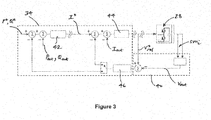
- High-level controller 34 may limit the active and reactive power transfer demands P*, Q* made of the voltage source converter 10 is illustrated, by way of example, in Figure 3 .
- a first regulator 42 establishes a current reference I * which, following a comparison with the actual current being produced I act , is processed by a second regulator 44 to establish the corresponding chain-link reference voltage v * ref , which the associated low-level controller 38 controls the corresponding chain-link converter 28 to produce.
- the evaluation module 40 compares the respective chain-link reference voltage v * ref the corresponding chain-link converter 28 is required to produce with the actual stepped variable voltage source v act provided by the said corresponding chain-link converter 28, and the output of the evaluation module 40 acts, as necessary, through a compensator 46 within the high-level controller 34 to either:
Landscapes
- Engineering & Computer Science (AREA)
- Power Engineering (AREA)
- Inverter Devices (AREA)
- Rectifiers (AREA)
- Supply And Distribution Of Alternating Current (AREA)
- Dc-Dc Converters (AREA)
Description
- This invention relates to a voltage source converter and to a method of operating a voltage source converter, preferably for use in high voltage direct current (HVDC) transmission.
- In HVDC power transmission networks alternating current (AC) power is typically converted to direct current (DC) power for transmission via overhead lines, under-sea cables and/or underground cables. This conversion removes the need to compensate for the AC capacitive load effects imposed by the power transmission medium, i.e. the transmission line or cable, and reduces the cost per kilometre of the lines and/or cables, and thus becomes cost-effective when power needs to be transmitted over a long distance.
- The conversion between DC power and AC power is utilized in power transmission networks where it is necessary to interconnect the DC and AC networks. In any such power transmission network, converters are required at each interface between AC and DC power to effect the required conversion from AC to DC or from DC to AC. Such converters may employ voltage source converters to perform power conversion.
- Document
EP 2 884 653 A1 discloses a three-phase converter with three converter limbs each including first and second limb portions. The converter further includes a controller configured to determine optimal limb portion currents and/or optimal limb portion voltage sources. The controller may be configured to reduce the level of current or voltage of a limb portion in case a fault has degraded the performance of this limb portion. The article NAMI Alireza et al: "Modular Multilevel Converters for HVDC Applications: Review on Converter Cells and Functionalities", IEEE Transactions on Power Electronics, Institute of Electrical and Electronics Engineers, vol. 30, No. 1, 1 January 2015, pages 18-36, XP011557523, ISSN 0885-8993, relates to voltage and current source modular multilevel converters - The present invention provides a voltage source converter according to claim 1 and a method of operating a voltage source converter according to claim 8. Preferred embodiments are defined in the dependent claims.
- J According to a first aspect of the invention there is provided a voltage source converter comprising:
- first and second DC terminals for connection to a DC network;
- at least one converter limb, the or each converter limb extending between the first and second DC terminals and including first and second limb portions separated by a respective AC terminal for connection to a corresponding phase of an AC network, each first limb portion extending between the first DC terminal and corresponding AC terminal, each second limb portion extending between the second DC terminal and corresponding AC terminal, each limb portion including a respective chain-link converter defined by a plurality of series-connected switching modules operable in combination to provide a stepped variable voltage source; and
- a control apparatus configured to coordinate operation of the chain-link converters to cause an exchange of power between the DC and AC networks, the control apparatus evaluating the combined performance of the switching modules within at least one chain-link converter and acting to modify the coordinated operation of the chain-link converters when the combined performance of the said switching modules becomes degraded to a predetermined extent.
- The inclusion of such a control apparatus within the voltage source converter of the invention desirably permits the continued transfer of power, both active and reactive, under conditions in which the performance of one or more switching modules within a given chain-link converter has become degraded, e.g. because of a sudden failure or ageing, which in turn provides for increased voltage source converter availability and reduced converter outage time, e.g. between scheduled maintenance periods.
- Optionally the control apparatus modifies the coordinated operation of the chain-link converters when the combined performance of the switching modules within at least one chain-link converter becomes degraded to a predetermined extent by varying the active and/or reactive power transfer demands made of the voltage source converter.
- Preferably the control apparatus modifies the coordinated operation of the chain-link converters by limiting the active and/or reactive power transfer demands made of the voltage source converter.
- The inclusion of a control apparatus having the foregoing features helps to ensure that the voltage source converter is able to continue operating in a stable manner, despite the degraded performance of one or more switching modules.
- The control apparatus may include:
- a high-level controller programmed to receive active and/or reactive power transfer demands that the voltage source converter is required to provide, and to establish a respective chain-link reference voltage for each chain-link converter that each respective chain-link converter is required to produce in order that coordinated operation of the chain-link converters causes the demanded power transfer between the DC and AC networks;
- at least one low-level controller programmed to control the operation of each switching module within at least one chain-link converter, whereby the said chain-link converter aims to provide a stepped variable voltage source equal to the corresponding required chain-link reference voltage; and
- an evaluation module configured to receive switching module performance information and programmed to evaluate the performance information to establish when the combined performance of the switching modules within the at least one chain-link converter has become degraded to a predetermined extent.
- In a preferred embodiment of the invention the evaluation module is programmed to instruct the high-level controller to modify the coordinated operation of the chain-link converters when the evaluation module establishes that the combined performance of the switching modules within the at least one chain-link converter has become degraded to a predetermined extent.
- Having a control apparatus configured as described hereinabove is advantageous because it separates out different aspects of the overall control of the voltage source converter in a manner that allows each to be optimised in terms of speed and efficiency.
- Preferably the evaluation module is programmed to instruct the high-level controller to operate the voltage source converter in a degraded mode in which the high-level controller limits the active and/or reactive power transfer demands made of the voltage source converter in order that the coordinated operation of the chain-link converters is modified.
- Having the voltage source converter operate in a degraded mode is desirable since it allows for the continued transfer of power by the voltage source converter on a temporary or long-term basis, depending on the severity of switching module degradation, until a subsequent maintenance period offers an opportunity to reinstate the full power transfer capability of the voltage source converter.
- Optionally the high-level controller limits the active and/or reactive power transfer demands by one of:
- reducing the active real and/or reactive power transfer demand; and
- reducing a current reference demand resulting from the active and/or reactive power transfer demand.
- Such steps can be readily implemented in a practicable manner.
- In a further preferred embodiment of the invention the evaluation module is programmed to evaluate the performance information for the switching modules within a given chain-link converter by comparing the respective chain-link reference voltage the given chain-link converter is required to produce with the actual stepped variable voltage source provided by the said given chain-link converter, and to establish that the combined performance of the switching modules within the given chain-link converter has become degraded to a predetermined extent when the actual stepped variable voltage source provided falls short of the corresponding chain-link reference voltage by more than a predetermined amount.
- Comparing the respective chain-link reference voltage with the actual stepped variable voltage source provided, which may be estimated or calculated based on individual switching module voltage measurements and their switching state, provides a reliable and readily implementable way of establishing when an undesired degree of switching module degradation has occurred, which then allows for the overall operation of the voltage source converter to be modified accordingly.
- According to a second aspect of the invention there is provided a method of operating a voltage source converter, the voltage source converter comprising:
- first and second DC terminals for connection to a DC network;
- at least one converter limb, the or each converter limb extending between the first and second DC terminals and including first and second limb portions separated by a respective AC terminal for connection to a corresponding phase of an AC network, each first limb portion extending between the first DC terminal and corresponding AC terminal, each second limb portion extending between the second DC terminal and corresponding AC terminal, each limb portion including a respective chain-link converter defined by a plurality of series-connected switching modules operable in combination to provide a stepped variable voltage source,
- wherein the method comprises the steps of:
- coordinating operation of the chain-link converters to cause an exchange of power between the DC and AC networks;
- evaluating the combined performance of the switching modules within at least one chain-link converter; and
- acting to modify the coordinated operation of the chain-link converters when the combined performance of the said switching modules becomes degraded to a predetermined extent.
- The method may include the step of modifying the coordinated operation of the chain-link converters when the combined performance of the switching modules within at least one chain-link converter becomes degraded to a predetermined extent by varying the active and/or reactive power transfer demands made of the voltage source converter.
- The method may include the step of modifying the coordinated operation of the chain-link converters by limiting the active and/or reactive power transfer demands made of the voltage source converter.
- The method may include the steps of:
- receiving active and/or reactive power transfer demands that the voltage source converter is required to provide;
- establishing a respective chain-link reference voltage for each chain-link converter that each respective chain-link converter is required to produce in order that coordinated operation of the chain-link converters causes the demanded power transfer between the DC and AC networks;
- controlling the operation of each switching module within at least one chain-link converter, whereby the said chain-link converter aims to provide a stepped variable voltage source equal to the corresponding required chain-link reference voltage; and
- receiving switching module performance information and evaluating the performance information to establish when the combined performance of the switching modules within the at least one chain-link converter has become degraded to a predetermined extent.
- The method may include the step of modifying the coordinated operation of the chain-link converters when it is established that the combined performance of the switching modules within the at least one chain-link converter has become degraded to a predetermined extent.
- The method may include the step of operating the voltage source converter in a degraded mode in which the active and/or reactive power transfer demands made of the voltage source converter are limited in order that the coordinated operation of the chain-link converters is modified.
- Optionally the method may further include the step of limiting the active and/or reactive power transfer demands by one of:
- reducing the active real and/or reactive power transfer demand; and
- reducing a current reference demand resulting from the active and/or reactive power transfer demand.
- The method may include the steps of evaluating the performance information for the switching modules within a given chain-link converter by comparing the respective chain-link reference voltage the given chain-link converter is required to produce with the actual stepped variable voltage source provided by the said given chain-link converter, and establishing that the combined performance of the switching modules within the given chain-link converter has become degraded to a predetermined extent when the actual stepped variable voltage source provided falls short of the corresponding chain-link reference voltage by more than a predetermined amount.
- The advantages of the voltage source converter of the first aspect of the invention and its embodiments apply mutatis mutandis to the method of the second aspect of the invention and its embodiments.
- There now follows a brief description of preferred embodiment of the invention, by way of non-limiting example, with reference being made to the following figures in which:
-
Figure 1 shows a schematic view of a voltage source converter according to an embodiment of the invention; -
Figure 2 shows an enlarged, schematic view of an evaluation module which forms a part of the voltage source converter shown inFigure 1 ; and -
Figure 3 shows an example of how a high-level controller which forms a part of the voltage source converter shown inFigure 1 may be programmed to modify the operation of the said voltage source converter. - The figures are not necessarily to scale, and certain features or figures may be shown exaggerated in scale or in schematic form in the interests of clarity and conciseness.
- The following embodiment of the invention is used primarily in HVDC applications, but it will be appreciated that embodiments of the invention may be applicable to other applications operating at different voltage levels.
- A voltage source converter according to an embodiment of the invention is shown in
Figure 1 and is designated generally by thereference numeral 10. - The
voltage source converter 10 includes first andsecond DC terminals - The
voltage source converter 10 also includes threeconverter limbs 18, only one of which is shown inFigure 1 . Eachconverter limb 18 extends between the first andsecond DC terminals respective AC terminal 24, again only one of which is shown inFigure 1 . TheAC terminals 24 are, in use, connected to a corresponding phase of a three-phase AC network 26. - In other embodiments of the invention (not shown) the voltage source converter may include fewer than or more than three converter limbs, the actual number of converter limbs corresponding to the number of phases within an associated AC network that the voltage source converter is intended, in use, to be connected with.
- Each first limb portion 20 extends between the
first DC terminal 12 and thecorresponding AC terminal 24, while each second limb portion 22 extends between thesecond DC terminal 14 and thecorresponding AC terminal 24. - Each limb portion 20, 22 includes a respective
chain link converter 28 that is defined by a plurality of series-connectedswitching modules 30. Each switchingmodule 30 includes a number of switching elements (not shown) that are connected in parallel with an energy storage device in the form of a capacitor (not shown). Each switching element includes a semiconductor device in the form of, e.g. an Insulated Gate Bipolar Transistor (IGBT), which is connected in parallel with an anti-parallel diode. It is, however, possible to use other semiconductor devices. - More particularly, in the embodiment shown each chain-
link converter 28 is defined by a plurality of series-connectedswitching modules 30 of a first type in which first and second pairs of switching elements and a capacitor are connected in a known full bridge arrangement to define a 4-quadrant bipolar module. Switching of the switching elements selectively inserts or bypasses the capacitor into the corresponding limb portion, i.e. selectively directs current through the capacitor or causes current to bypass the capacitor, such that the first type of switchingmodule 30 can provide zero, positive or negative voltage and can conduct current in two directions. - A second type of switching module is one in which only a first pair of switching elements is connected in parallel with a capacitor in a known half-bridge arrangement to define a 2-quadrant unipolar module. In a similar manner to the first type of switching
module 30, switching of the switching elements again inserts or bypasses the capacitor into the corresponding limb portion, i.e. selectively directs current through the capacitor or causes current to bypass the capacitor, such that the second type of switching module can provide zero or positive voltage and can conduct current in two directions. - In other embodiments of the invention, one or more chain-link converters may be made up entirely of the second type of switching module, or of a combination of first and second types of switching module.
- In any event, by virtue of selectively inserting or bypassing the energy storage device (i.e. the corresponding capacitor) of each switching
module 30 into a corresponding limb portion to thereby control a voltage across eachindividual switching module 30, it is possible to build up a combined voltage across each chain-link converter 28 by combining the individual voltage available from each switchingmodule 30. - Accordingly, the switching
modules 30 of a respective chain-link converter 28 are operable in combination to provide a stepped variable voltage source. - In addition to the foregoing, the
voltage source converter 10 of the invention includes acontrol apparatus 32 which is configured to coordinate operation of the chain-link converters to cause an exchange of power between the DC and AC networks (16, 26). More particularly, thecontrol apparatus 32 includes a high-level controller 34 that is programmed to receive active and reactive power transfer demands P*, Q* that thevoltage source converter 10 is required to provide. In the embodiment shown, the high-level controller 34 receives the active and reactive power demands P. Q from ahuman machine interface 36, although this need not necessarily be the case. Furthermore, in other embodiments of the invention the high-level controller may receive only one of an active power transfer demand or a reactive power transfer demand. - In any event, however, the high-
level controller 34 is further programmed to establish a respective chain-link reference voltage v* ref for each chain-link converter 28 that each respective chain-link converter 28 is required to produce in order that coordinated operation of the chain-link converters 28 causes the demanded power transfer between the DC andAC networks 16, 26. - In addition to the foregoing, the
control apparatus 32 includes six low-level controllers 38, only two of which are shown inFigure 1 . Each low-level controller 38 is programmed to control the operation of each switchingmodule 30 within a corresponding single chain-link converter 28, whereby the said corresponding single chain-link converter 28 aims to provide a stepped variable voltage source vact equal to the corresponding required chain-link reference voltage v* ref. - In other embodiments of the invention (not shown) one or more low-level controllers may be programmed to control the switching of switching elements within the switching modules of more than one chain-link converter.
- The
control apparatus 32 is additionally configured to evaluate the combined performance of the switchingmodules 30 within each chain-link converter 28, although in some other embodiments it may not be each chain-link converter, and to modify the coordinated operation of the chain-link converters 28 when the combined performance of the switchingmodules 30 within a given chain-link converter becomes degraded to a predetermined extent. - In particular, the
control apparatus 32 modifies the coordinated operation of the chain-link converters 28 by varying the active and reactive power transfer demands P*, Q* made of thevoltage source converter 10, and more particularly still modifies the coordinated operation of the chain-link converters 28 by limiting the active and reactive power transfer demands P*, Q* made of thevoltage source converter 10. - To that end, the
control apparatus 32 includes anevaluation module 40 that is configured to receive switching module performance information smi, which typically includes individual switching module voltages, statuses, and health indicators. - The
evaluation module 40 is additionally programmed to evaluate the performance information smi and thereby establish when the combined performance of the switchingmodules 30 within each given chain-link converter 28 has become degraded to a predetermined extent. - More particularly, the
evaluation module 40 is programmed, as shown inFigure 2 , to evaluate the performance information smi for the switchingmodules 30 within a given chain-link converter 28 by comparing the respective chain-link reference voltage v* ref the given chain-link converter 28 is required to produce with the actual stepped variable voltage source vact provided by the said given chain-link converter 28. - Thereafter, the
evaluation module 40 establishes that the combined performance of the switchingmodules 30 within the given chain-link converter 28 has become degraded to a predetermined extent when the actual stepped variable voltage source vact provided falls short of the corresponding chain-link reference voltage v* ref by more than a predetermined amount. - By way of example, the predetermined amount is typically 3%, i.e. the
evaluation module 40 establishes that the combined performance of the switchingmodules 30 within the given chain-link converter 28 has become degraded to a predetermined extent when the peak value of the actual stepped variable voltage source vact is less than or equal to 97% of the peak value of the corresponding chain-link reference voltage v* ref. - Once the
evaluation module 40 has established that the combined performance of the switchingmodules 30 within a given chain-link converter 28 has become degraded to a predetermined extent, theevaluation module 40 is still further programmed to instruct the high-level controller 34 to modify the coordinated operation of the chain-link converters 28. - More particularly, the
evaluation module 40 is further programmed, as illustrated schematically inFigure 2 , to instruct the high-level controller 34 to switch from operating thevoltage source converter 10 in a normal mode N, to operate thevoltage source converter 10 in a degraded mode D. When operating thevoltage source converter 10 in the degraded mode D, the high-level controller 34 limits the active and reactive power transfer demands P*, Q* made of thevoltage source converter 10. - One way in which the high-
level controller 34 may limit the active and reactive power transfer demands P*, Q* made of thevoltage source converter 10 is illustrated, by way of example, inFigure 3 . - Following a comparison of the active and reactive power transfer demands P*, Q* with the actual active and reactive power Pact, Qact being transferred, a
first regulator 42 establishes a current reference I* which, following a comparison with the actual current being produced Iact, is processed by a second regulator 44 to establish the corresponding chain-link reference voltage v* ref, which the associated low-level controller 38 controls the corresponding chain-link converter 28 to produce. - As described above, the
evaluation module 40 compares the respective chain-link reference voltage v* ref the corresponding chain-link converter 28 is required to produce with the actual stepped variable voltage source vact provided by the said corresponding chain-link converter 28, and the output of theevaluation module 40 acts, as necessary, through acompensator 46 within the high-level controller 34 to either: - reduce the active real and reactive power transfer demand P*, Q*; or
- reduce the current reference demand I* resulting from the active and reactive power transfer demand P*, Q*.
Claims (13)
- A voltage source converter (10) comprising:first and second DC terminals (12, 14) for connection to a DC network (16); andat least one converter limb (18), the or each converter limb (18) extending between and being connected to the first and second DC terminals (12, 14) and including first and second limb portions (20, 22) separated by a respective AC terminal (24) for connection to a corresponding phase of an AC network (26), each first limb portion (20) extending between the first DC terminal (12) and corresponding AC terminal (24), each second limb portion (22) extending between and being connected to the second DC terminal (14) and corresponding AC terminal (24); the voltage source converter (10) being characterized in thateach limb portion (20, 22) includes a respective chain-link converter (28) defined by a plurality of series-connected switching modules (30) configured to operate in combination to provide a stepped variable voltage source; andin that it further comprises a control apparatus (32) configured to coordinate operation of the chain-link converters (28) to cause an exchange of power between the DC and AC networks (16, 26), the control apparatus (32) being configured to evaluate a combined performance of the switching modules (30) within at least one chain-link converter (28) and being configured to modify a coordinated operation of the chain-link converters (28) when the combined performance of the said switching modules (30) becomes degraded to a predetermined extent by varying active and/or reactive power transfer demands (P*, Q*) that the voltage source converter (10) is required to provide.
- A voltage source converter (10) according to Claim 1 wherein the control apparatus (32) is configured to modify the coordinated operation of the chain-link converters (28) by limiting the active and/or reactive power transfer demands (P*, Q*) that the voltage source converter (10) is required to provide.
- A voltage source converter (10) according to claim 1 or 2 wherein the control apparatus (32) includes:a high-level controller (34) configured to be programmed to receive said active and/or reactive power transfer demands (P*, Q*) that the voltage source converter (10) is required to provide, and configured to establish a respective chain-link reference voltage (v* ref) for each chain-link converter (28) that each respective chain-link converter (28) is required to produce in order that coordinated operation of the chain-link converters (28) causes the demanded power transfer between the DC and AC networks (16, 26);at least one low-level controller (38) configured to be programmed to control the operation of each switching module (30) within at least one chain-link converter (28), whereby the said chain-link converter (28) is configured to provide said stepped variable voltage source equal to the corresponding required chain-link reference voltage (v* ref); andan evaluation module (40) configured to receive switching module performance information (smi) and programmed to evaluate the performance information (smi) to establish when the combined performance of the switching modules (30) within the at least one chain-link converter (28) has become degraded to said predetermined extent.
- A voltage source converter (10) according to Claim 3 wherein the evaluation module (40) is programmed to instruct the high-level controller (34) to modify the coordinated operation of the chain-link converters (28) when the evaluation module (40) establishes that the combined performance of the switching modules (30) within the at least one chain-link converter (28) has become degraded to said predetermined extent.
- A voltage source converter (10) according to Claim 4 wherein the evaluation module (40) is configured to be programmed to instruct the high-level controller (34) to operate the voltage source converter (10) in a degraded mode (D) in which the high-level controller (34) is configured to limit the active and/or reactive power transfer demands (P*, Q*) that the voltage source converter (10) is required to provide in order that the coordinated operation of the chain-link converters (28) is modified.
- A voltage source converter (10) according to Claim 5 wherein the high-level controller (34) is configured to limit the active and/or reactive power transfer demands (P*, Q*) by one of:reducing the active real and/or reactive power transfer demands (P*, Q*); andreducing a current reference demand (I*) resulting from the active and/or reactive power transfer demands (P*, Q*).
- A voltage source converter (10) according to any of Claims 3 to 6 wherein the evaluation module (40) is configured to be
programmed to evaluate the performance information (smi) for the switching modules (30) within a given chain-link converter (28) by comparing the respective chain-link reference voltage (v* ref) the given chain-link converter (28) is required to produce with the actual stepped variable voltage source (vact) provided by said given chain-link converter (28), and to establish that the combined performance of the switching modules (30) within the given chain-link converter (28) has become degraded to said predetermined extent when the actual stepped variable voltage source (vact) provided falls short of the corresponding chain-link reference voltage (v* ref) by more than a predetermined amount. - A method of operating a voltage source converter (10), the voltage source converter (10) comprising:first and second DC terminals (12, 14) for connection to a DC network (16);at least one converter limb (18), the or each converter limb (18) extending between and being connected to the first and second DC terminals (12, 14) and including first and second limb portions (20, 22) separated by a respective AC terminal (24) for connection to a corresponding phase of an AC network (26), each first limb portion (20) extending between and being connected to the first DC terminal (12) and corresponding AC terminal (24), each second limb portion (22) extending between and being connected to the second DC terminal (14) and corresponding AC terminal (24), each limb portion (20, 22) including a respective chain-link converter (28) defined by a plurality of series-connected switching modules (30) operatingin combination to provide a stepped variable voltage source,the method being characterized in that it comprises the steps of:coordinating operation of the chain-link converters (28) to cause an exchange of power between the DC and AC networks (16, 26);evaluating a combined performance of the switching modules (30) within at least one chain-link converter (28); andacting to modify a coordinated operation of the chain-link converters (28) when the combined performance of the said switching modules (30) becomes degraded to a predetermined extent by varying active and/or reactive power transfer demands (P*, Q*) that the voltage source converter (10) is required to provide.
- A method according to Claim 8 including the step of modifying the coordinated operation of the chain-link converters (28) by limiting the active and/or reactive power transfer demands (P*, Q*) that the voltage source converter (10) is required to provide.
- A method according to any one of Claims 8 and 9 including the steps of:receiving said active and/or reactive power transfer demands (P*, Q*) that the voltage source converter (10) is required to provide;establishing a respective chain-link reference voltage (v* ref) for each chain-link converter (28) that each respective chain-link converter (28) is required to produce in order that coordinated operation of the chain-link converters (28) causes the demanded power transfer between the DC and AC networks (16, 26);controlling the operation of each switching module (30) within at least one chain-link converter (28), whereby the said chain-link converter (28) aims to provide said stepped variable voltage source equal to the corresponding required chain-link reference voltage (v* ref); andreceiving switching module performance information (smi) and evaluating the performance information (smi) to establish when the combined performance of the switching modules (30) within the at least one chain-link converter (28) has become degraded to said predetermined extent.
- A method according to Claim 10 including the step of modifying the coordinated operation of the chain-link converters (28) when it is established that the combined performance of the switching modules (30) within the at least one chain-link converter (28) has become degraded to said predetermined extent.
- A method according to Claim 11 including the step of operating the voltage source converter (10) in a degraded mode (D) in which the active and/or reactive power transfer demands (P*, Q*) that the voltage source converter (10) is required to provide are limited in order that the coordinated operation of the chain-link converters (28) is modified, and optionally wherein the method further includes the step of limiting the active and/or reactive power transfer demands (P*, Q*) by one of:reducing the active real and/or reactive power transfer demands (P*, Q*); andreducing a current reference demand (I*) resulting from the active and/or reactive power transfer demands (P*. Q*).
- A method according to any one of Claims 10 to 12 including the steps of evaluating the performance information (smi) for the switching modules (30) within a given chain-link converter (28) by comparing the respective chain-link reference voltage (v* ref) the given chain-link converter (28) is required to produce with the actual stepped variable voltage source (vact) provided by said given chain-link converter (28), and establishing that the combined performance of the switching modules (30) within the given chain-link converter (28) has become degraded to said predetermined extent when the actual stepped variable voltage source (vact) provided falls short of the corresponding chain-link reference voltage (v* ref) by more than a predetermined amount.
Priority Applications (3)
| Application Number | Priority Date | Filing Date | Title |
|---|---|---|---|
| EP18190658.7A EP3614552B1 (en) | 2018-08-24 | 2018-08-24 | Voltage source converter |
| PCT/EP2019/072107 WO2020038870A1 (en) | 2018-08-24 | 2019-08-19 | Voltage source converter |
| US17/270,814 US11728744B2 (en) | 2018-08-24 | 2019-08-19 | Voltage source converter for use in power transmission networks |
Applications Claiming Priority (1)
| Application Number | Priority Date | Filing Date | Title |
|---|---|---|---|
| EP18190658.7A EP3614552B1 (en) | 2018-08-24 | 2018-08-24 | Voltage source converter |
Publications (2)
| Publication Number | Publication Date |
|---|---|
| EP3614552A1 EP3614552A1 (en) | 2020-02-26 |
| EP3614552B1 true EP3614552B1 (en) | 2021-05-19 |
Family
ID=63405029
Family Applications (1)
| Application Number | Title | Priority Date | Filing Date |
|---|---|---|---|
| EP18190658.7A Active EP3614552B1 (en) | 2018-08-24 | 2018-08-24 | Voltage source converter |
Country Status (3)
| Country | Link |
|---|---|
| US (1) | US11728744B2 (en) |
| EP (1) | EP3614552B1 (en) |
| WO (1) | WO2020038870A1 (en) |
Family Cites Families (29)
| Publication number | Priority date | Publication date | Assignee | Title |
|---|---|---|---|---|
| CA2754960C (en) | 2009-03-11 | 2016-08-23 | Abb Technology Ag | A modular voltage source converter |
| US8837185B2 (en) * | 2010-02-11 | 2014-09-16 | Siemens Aktiengesellschaft | Control of a modular converter having distributed energy stores with the aid of an observer for the currents and an estimating unit for the intermediate circuit energy |
| CA2793701C (en) * | 2010-04-08 | 2017-05-16 | Alstom Technology Ltd | Hybrid hvdc converter |
| CN103283140B (en) * | 2010-10-27 | 2015-07-29 | 阿尔斯通技术有限公司 | Modular multilevel converter |
| DK2806552T3 (en) * | 2012-01-18 | 2017-01-09 | Toshiba Mitsubishi-Electric Ind Systems Corp | Energy converter layout |
| US9219426B2 (en) * | 2012-02-09 | 2015-12-22 | Hitachi, Ltd. | Switching element, power converter, direct current transmission system, current control device, method of controlling power converter, and method of controlling current in voltage source converter |
| KR101584057B1 (en) | 2012-07-06 | 2016-01-22 | 에이비비 테크놀로지 아게 | Controlling a modular converter |
| WO2014033155A1 (en) * | 2012-08-28 | 2014-03-06 | Abb Technology Ag | Controlling a modular converter in two stages |
| EP2782239A1 (en) * | 2013-03-21 | 2014-09-24 | Alstom Technology Ltd | Power electronic converter |
| GB2518853B (en) * | 2013-10-02 | 2016-01-27 | Alstom Technology Ltd | Voltage source converter |
| EP2858231B1 (en) * | 2013-10-07 | 2019-09-11 | General Electric Technology GmbH | Voltage source converter |
| EP2863534B1 (en) * | 2013-10-16 | 2018-09-26 | General Electric Technology GmbH | Voltage source converter |
| EP2884653B1 (en) * | 2013-12-12 | 2022-10-26 | General Electric Technology GmbH | Improvements in or relating to the control of converters |
| EP2916442B1 (en) * | 2014-03-04 | 2019-07-24 | General Electric Technology GmbH | A voltage source converter |
| EP2988406A1 (en) * | 2014-08-19 | 2016-02-24 | Alstom Technology Ltd | Improvements in or relating to the control of converters |
| CN113872425A (en) * | 2015-03-30 | 2021-12-31 | 通用电器技术有限公司 | Control of voltage source converter |
| EP3096446A1 (en) * | 2015-05-22 | 2016-11-23 | General Electric Technology GmbH | A method of controlling a converter |
| US10079558B2 (en) * | 2016-04-08 | 2018-09-18 | American Superconductor Corporation | Switching scheme for static synchronous compensators using cascaded H-bridge converters |
| GB2549462B (en) * | 2016-04-13 | 2020-02-19 | General Electric Technology Gmbh | Voltage source converter |
| GB2550421A (en) * | 2016-05-20 | 2017-11-22 | General Electric Technology Gmbh | Control of voltage source converters |
| FR3053854B1 (en) * | 2016-07-05 | 2018-08-17 | Supergrid Institute | MODULE FOR CONTROLLING THE INTERNAL ENERGY OF A CONVERTER |
| EP3340453B1 (en) * | 2016-12-22 | 2021-03-10 | General Electric Technology GmbH | Method of configuring a closed-loop control system |
| EP3361619B1 (en) * | 2017-02-09 | 2019-10-09 | General Electric Technology GmbH | Voltage source converter |
| WO2018229857A1 (en) * | 2017-06-13 | 2018-12-20 | 三菱電機株式会社 | Power conversion system |
| FR3068842B1 (en) * | 2017-07-07 | 2022-03-04 | Inst Supergrid | CONVERTER EQUIPPED WITH AN ENERGY MANAGEMENT MODULE IN ALTERNATIVE PART |
| US11404973B2 (en) * | 2018-12-19 | 2022-08-02 | Di Shi | Generalized equivalent circuit model of MMC-HVDC for power system simulation |
| EP3713073A1 (en) * | 2019-03-19 | 2020-09-23 | Siemens Aktiengesellschaft | Converter and method for controlling same |
| EP3780366A1 (en) * | 2019-08-13 | 2021-02-17 | Vestas Wind Systems A/S | Dc chopper for mmc cell with integrated chopper resistor |
| US11824461B2 (en) * | 2020-06-24 | 2023-11-21 | North Carolina State University | MMC submodules scale-up methodology for MV and HV power conversion system applications |
-
2018
- 2018-08-24 EP EP18190658.7A patent/EP3614552B1/en active Active
-
2019
- 2019-08-19 US US17/270,814 patent/US11728744B2/en active Active
- 2019-08-19 WO PCT/EP2019/072107 patent/WO2020038870A1/en not_active Ceased
Also Published As
| Publication number | Publication date |
|---|---|
| US11728744B2 (en) | 2023-08-15 |
| WO2020038870A1 (en) | 2020-02-27 |
| US20210249969A1 (en) | 2021-08-12 |
| EP3614552A1 (en) | 2020-02-26 |
Similar Documents
| Publication | Publication Date | Title |
|---|---|---|
| Friedrich | Modern HVDC PLUS application of VSC in modular multilevel converter topology | |
| EP2067229B1 (en) | Conversion of ac lines to hvdc lines | |
| EP2863534B1 (en) | Voltage source converter | |
| Gwon et al. | Mitigation of voltage unbalance by using static load transfer switch in bipolar low voltage DC distribution system | |
| CA2759818C (en) | Method and arrangement to determine the cell capacitor voltage of a cell of a multi-cell power converter | |
| EP4138251B1 (en) | Power supply system | |
| US10284080B2 (en) | Column-switched multi-module DC-to-DC power transformation system | |
| EP3614552B1 (en) | Voltage source converter | |
| Plihal et al. | A study on the implementation of HVDC for Power system interconnection | |
| EP3829047A1 (en) | Converter | |
| EP3790143A1 (en) | Electrical assembly | |
| CN106411249A (en) | Photovoltaic power generation system and control method thereof | |
| US20240171072A1 (en) | Dc/dc converter device for a wind turbine, an electric drive system, or an industrial dc supply network and operating method | |
| WO2024167492A1 (en) | Cell bypass for variable frequency drives | |
| US11121640B2 (en) | Systems, methods, and apparatus for controlling a voltage source converter | |
| WO2021099383A1 (en) | Improvements in or relating to power dissipating converters | |
| US6861825B2 (en) | Hybrid AC/DC system for electric power transmission | |
| US12003169B2 (en) | Chain-link modules for voltage source converters | |
| US20260100584A1 (en) | System and method for controlling a power electronics device in a power transmission network | |
| WO2020102373A1 (en) | Voltage source converter | |
| US20230402935A1 (en) | Electrical assembly | |
| EP4213364A1 (en) | Switching valve | |
| CN116154837A (en) | Inverter, its control method, and power supply system | |
| Singh | Analysis of DC Fault in Multiterminal HVDC Grid |
Legal Events
| Date | Code | Title | Description |
|---|---|---|---|
| PUAI | Public reference made under article 153(3) epc to a published international application that has entered the european phase |
Free format text: ORIGINAL CODE: 0009012 |
|
| STAA | Information on the status of an ep patent application or granted ep patent |
Free format text: STATUS: THE APPLICATION HAS BEEN PUBLISHED |
|
| AK | Designated contracting states |
Kind code of ref document: A1 Designated state(s): AL AT BE BG CH CY CZ DE DK EE ES FI FR GB GR HR HU IE IS IT LI LT LU LV MC MK MT NL NO PL PT RO RS SE SI SK SM TR |
|
| AX | Request for extension of the european patent |
Extension state: BA ME |
|
| STAA | Information on the status of an ep patent application or granted ep patent |
Free format text: STATUS: REQUEST FOR EXAMINATION WAS MADE |
|
| 17P | Request for examination filed |
Effective date: 20200821 |
|
| RBV | Designated contracting states (corrected) |
Designated state(s): AL AT BE BG CH CY CZ DE DK EE ES FI FR GB GR HR HU IE IS IT LI LT LU LV MC MK MT NL NO PL PT RO RS SE SI SK SM TR |
|
| RIN1 | Information on inventor provided before grant (corrected) |
Inventor name: BRIFF, PABLO, ARIEL Inventor name: BREHAUT, STEPHANE, PIERRE Inventor name: JASMIN, OMAR Inventor name: DE PREVILLE, GUILLAUME Inventor name: ZHANG, RICHARD S. Inventor name: DANG, HUY QUOC SI |
|
| GRAP | Despatch of communication of intention to grant a patent |
Free format text: ORIGINAL CODE: EPIDOSNIGR1 |
|
| STAA | Information on the status of an ep patent application or granted ep patent |
Free format text: STATUS: GRANT OF PATENT IS INTENDED |
|
| RIC1 | Information provided on ipc code assigned before grant |
Ipc: H02M 1/32 20070101ALI20201113BHEP Ipc: H02M 7/483 20070101AFI20201113BHEP |
|
| INTG | Intention to grant announced |
Effective date: 20201216 |
|
| GRAS | Grant fee paid |
Free format text: ORIGINAL CODE: EPIDOSNIGR3 |
|
| GRAA | (expected) grant |
Free format text: ORIGINAL CODE: 0009210 |
|
| STAA | Information on the status of an ep patent application or granted ep patent |
Free format text: STATUS: THE PATENT HAS BEEN GRANTED |
|
| AK | Designated contracting states |
Kind code of ref document: B1 Designated state(s): AL AT BE BG CH CY CZ DE DK EE ES FI FR GB GR HR HU IE IS IT LI LT LU LV MC MK MT NL NO PL PT RO RS SE SI SK SM TR |
|
| REG | Reference to a national code |
Ref country code: GB Ref legal event code: FG4D |
|
| REG | Reference to a national code |
Ref country code: CH Ref legal event code: EP |
|
| REG | Reference to a national code |
Ref country code: DE Ref legal event code: R096 Ref document number: 602018017195 Country of ref document: DE |
|
| REG | Reference to a national code |
Ref country code: AT Ref legal event code: REF Ref document number: 1394969 Country of ref document: AT Kind code of ref document: T Effective date: 20210615 |
|
| REG | Reference to a national code |
Ref country code: IE Ref legal event code: FG4D |
|
| REG | Reference to a national code |
Ref country code: SE Ref legal event code: TRGR |
|
| REG | Reference to a national code |
Ref country code: LT Ref legal event code: MG9D |
|
| REG | Reference to a national code |
Ref country code: AT Ref legal event code: MK05 Ref document number: 1394969 Country of ref document: AT Kind code of ref document: T Effective date: 20210519 |
|
| REG | Reference to a national code |
Ref country code: NL Ref legal event code: MP Effective date: 20210519 |
|
| PG25 | Lapsed in a contracting state [announced via postgrant information from national office to epo] |
Ref country code: LT Free format text: LAPSE BECAUSE OF FAILURE TO SUBMIT A TRANSLATION OF THE DESCRIPTION OR TO PAY THE FEE WITHIN THE PRESCRIBED TIME-LIMIT Effective date: 20210519 Ref country code: HR Free format text: LAPSE BECAUSE OF FAILURE TO SUBMIT A TRANSLATION OF THE DESCRIPTION OR TO PAY THE FEE WITHIN THE PRESCRIBED TIME-LIMIT Effective date: 20210519 Ref country code: FI Free format text: LAPSE BECAUSE OF FAILURE TO SUBMIT A TRANSLATION OF THE DESCRIPTION OR TO PAY THE FEE WITHIN THE PRESCRIBED TIME-LIMIT Effective date: 20210519 Ref country code: AT Free format text: LAPSE BECAUSE OF FAILURE TO SUBMIT A TRANSLATION OF THE DESCRIPTION OR TO PAY THE FEE WITHIN THE PRESCRIBED TIME-LIMIT Effective date: 20210519 Ref country code: BG Free format text: LAPSE BECAUSE OF FAILURE TO SUBMIT A TRANSLATION OF THE DESCRIPTION OR TO PAY THE FEE WITHIN THE PRESCRIBED TIME-LIMIT Effective date: 20210819 |
|
| PG25 | Lapsed in a contracting state [announced via postgrant information from national office to epo] |
Ref country code: IS Free format text: LAPSE BECAUSE OF FAILURE TO SUBMIT A TRANSLATION OF THE DESCRIPTION OR TO PAY THE FEE WITHIN THE PRESCRIBED TIME-LIMIT Effective date: 20210919 Ref country code: GR Free format text: LAPSE BECAUSE OF FAILURE TO SUBMIT A TRANSLATION OF THE DESCRIPTION OR TO PAY THE FEE WITHIN THE PRESCRIBED TIME-LIMIT Effective date: 20210820 Ref country code: LV Free format text: LAPSE BECAUSE OF FAILURE TO SUBMIT A TRANSLATION OF THE DESCRIPTION OR TO PAY THE FEE WITHIN THE PRESCRIBED TIME-LIMIT Effective date: 20210519 Ref country code: NO Free format text: LAPSE BECAUSE OF FAILURE TO SUBMIT A TRANSLATION OF THE DESCRIPTION OR TO PAY THE FEE WITHIN THE PRESCRIBED TIME-LIMIT Effective date: 20210819 Ref country code: PL Free format text: LAPSE BECAUSE OF FAILURE TO SUBMIT A TRANSLATION OF THE DESCRIPTION OR TO PAY THE FEE WITHIN THE PRESCRIBED TIME-LIMIT Effective date: 20210519 Ref country code: PT Free format text: LAPSE BECAUSE OF FAILURE TO SUBMIT A TRANSLATION OF THE DESCRIPTION OR TO PAY THE FEE WITHIN THE PRESCRIBED TIME-LIMIT Effective date: 20210920 Ref country code: RS Free format text: LAPSE BECAUSE OF FAILURE TO SUBMIT A TRANSLATION OF THE DESCRIPTION OR TO PAY THE FEE WITHIN THE PRESCRIBED TIME-LIMIT Effective date: 20210519 |
|
| PG25 | Lapsed in a contracting state [announced via postgrant information from national office to epo] |
Ref country code: NL Free format text: LAPSE BECAUSE OF FAILURE TO SUBMIT A TRANSLATION OF THE DESCRIPTION OR TO PAY THE FEE WITHIN THE PRESCRIBED TIME-LIMIT Effective date: 20210519 |
|
| PG25 | Lapsed in a contracting state [announced via postgrant information from national office to epo] |
Ref country code: EE Free format text: LAPSE BECAUSE OF FAILURE TO SUBMIT A TRANSLATION OF THE DESCRIPTION OR TO PAY THE FEE WITHIN THE PRESCRIBED TIME-LIMIT Effective date: 20210519 Ref country code: ES Free format text: LAPSE BECAUSE OF FAILURE TO SUBMIT A TRANSLATION OF THE DESCRIPTION OR TO PAY THE FEE WITHIN THE PRESCRIBED TIME-LIMIT Effective date: 20210519 Ref country code: SK Free format text: LAPSE BECAUSE OF FAILURE TO SUBMIT A TRANSLATION OF THE DESCRIPTION OR TO PAY THE FEE WITHIN THE PRESCRIBED TIME-LIMIT Effective date: 20210519 Ref country code: SM Free format text: LAPSE BECAUSE OF FAILURE TO SUBMIT A TRANSLATION OF THE DESCRIPTION OR TO PAY THE FEE WITHIN THE PRESCRIBED TIME-LIMIT Effective date: 20210519 Ref country code: DK Free format text: LAPSE BECAUSE OF FAILURE TO SUBMIT A TRANSLATION OF THE DESCRIPTION OR TO PAY THE FEE WITHIN THE PRESCRIBED TIME-LIMIT Effective date: 20210519 Ref country code: CZ Free format text: LAPSE BECAUSE OF FAILURE TO SUBMIT A TRANSLATION OF THE DESCRIPTION OR TO PAY THE FEE WITHIN THE PRESCRIBED TIME-LIMIT Effective date: 20210519 Ref country code: RO Free format text: LAPSE BECAUSE OF FAILURE TO SUBMIT A TRANSLATION OF THE DESCRIPTION OR TO PAY THE FEE WITHIN THE PRESCRIBED TIME-LIMIT Effective date: 20210519 |
|
| REG | Reference to a national code |
Ref country code: DE Ref legal event code: R097 Ref document number: 602018017195 Country of ref document: DE |
|
| PLBE | No opposition filed within time limit |
Free format text: ORIGINAL CODE: 0009261 |
|
| STAA | Information on the status of an ep patent application or granted ep patent |
Free format text: STATUS: NO OPPOSITION FILED WITHIN TIME LIMIT |
|
| REG | Reference to a national code |
Ref country code: CH Ref legal event code: PL |
|
| PG25 | Lapsed in a contracting state [announced via postgrant information from national office to epo] |
Ref country code: MC Free format text: LAPSE BECAUSE OF FAILURE TO SUBMIT A TRANSLATION OF THE DESCRIPTION OR TO PAY THE FEE WITHIN THE PRESCRIBED TIME-LIMIT Effective date: 20210519 |
|
| REG | Reference to a national code |
Ref country code: BE Ref legal event code: MM Effective date: 20210831 |
|
| 26N | No opposition filed |
Effective date: 20220222 |
|
| PG25 | Lapsed in a contracting state [announced via postgrant information from national office to epo] |
Ref country code: LI Free format text: LAPSE BECAUSE OF NON-PAYMENT OF DUE FEES Effective date: 20210831 Ref country code: CH Free format text: LAPSE BECAUSE OF NON-PAYMENT OF DUE FEES Effective date: 20210831 |
|
| PG25 | Lapsed in a contracting state [announced via postgrant information from national office to epo] |
Ref country code: IS Free format text: LAPSE BECAUSE OF FAILURE TO SUBMIT A TRANSLATION OF THE DESCRIPTION OR TO PAY THE FEE WITHIN THE PRESCRIBED TIME-LIMIT Effective date: 20210919 Ref country code: LU Free format text: LAPSE BECAUSE OF NON-PAYMENT OF DUE FEES Effective date: 20210824 Ref country code: AL Free format text: LAPSE BECAUSE OF FAILURE TO SUBMIT A TRANSLATION OF THE DESCRIPTION OR TO PAY THE FEE WITHIN THE PRESCRIBED TIME-LIMIT Effective date: 20210519 |
|
| PG25 | Lapsed in a contracting state [announced via postgrant information from national office to epo] |
Ref country code: IE Free format text: LAPSE BECAUSE OF NON-PAYMENT OF DUE FEES Effective date: 20210824 Ref country code: BE Free format text: LAPSE BECAUSE OF NON-PAYMENT OF DUE FEES Effective date: 20210831 |
|
| P01 | Opt-out of the competence of the unified patent court (upc) registered |
Effective date: 20230522 |
|
| PG25 | Lapsed in a contracting state [announced via postgrant information from national office to epo] |
Ref country code: CY Free format text: LAPSE BECAUSE OF FAILURE TO SUBMIT A TRANSLATION OF THE DESCRIPTION OR TO PAY THE FEE WITHIN THE PRESCRIBED TIME-LIMIT Effective date: 20210519 |
|
| PG25 | Lapsed in a contracting state [announced via postgrant information from national office to epo] |
Ref country code: HU Free format text: LAPSE BECAUSE OF FAILURE TO SUBMIT A TRANSLATION OF THE DESCRIPTION OR TO PAY THE FEE WITHIN THE PRESCRIBED TIME-LIMIT; INVALID AB INITIO Effective date: 20180824 |
|
| PG25 | Lapsed in a contracting state [announced via postgrant information from national office to epo] |
Ref country code: MK Free format text: LAPSE BECAUSE OF FAILURE TO SUBMIT A TRANSLATION OF THE DESCRIPTION OR TO PAY THE FEE WITHIN THE PRESCRIBED TIME-LIMIT Effective date: 20210519 |
|
| PG25 | Lapsed in a contracting state [announced via postgrant information from national office to epo] |
Ref country code: MT Free format text: LAPSE BECAUSE OF FAILURE TO SUBMIT A TRANSLATION OF THE DESCRIPTION OR TO PAY THE FEE WITHIN THE PRESCRIBED TIME-LIMIT Effective date: 20210519 |
|
| PGFP | Annual fee paid to national office [announced via postgrant information from national office to epo] |
Ref country code: DE Payment date: 20250724 Year of fee payment: 8 |
|
| PGFP | Annual fee paid to national office [announced via postgrant information from national office to epo] |
Ref country code: IT Payment date: 20250723 Year of fee payment: 8 |
|
| PGFP | Annual fee paid to national office [announced via postgrant information from national office to epo] |
Ref country code: GB Payment date: 20250724 Year of fee payment: 8 |
|
| PGFP | Annual fee paid to national office [announced via postgrant information from national office to epo] |
Ref country code: FR Payment date: 20250725 Year of fee payment: 8 |
|
| PGFP | Annual fee paid to national office [announced via postgrant information from national office to epo] |
Ref country code: SE Payment date: 20250723 Year of fee payment: 8 |
|
| PG25 | Lapsed in a contracting state [announced via postgrant information from national office to epo] |
Ref country code: TR Free format text: LAPSE BECAUSE OF FAILURE TO SUBMIT A TRANSLATION OF THE DESCRIPTION OR TO PAY THE FEE WITHIN THE PRESCRIBED TIME-LIMIT Effective date: 20210519 |