EP3614208A1 - Optical sensor and image forming apparatus - Google Patents
Optical sensor and image forming apparatus Download PDFInfo
- Publication number
- EP3614208A1 EP3614208A1 EP19191397.9A EP19191397A EP3614208A1 EP 3614208 A1 EP3614208 A1 EP 3614208A1 EP 19191397 A EP19191397 A EP 19191397A EP 3614208 A1 EP3614208 A1 EP 3614208A1
- Authority
- EP
- European Patent Office
- Prior art keywords
- light
- image
- led
- image forming
- optical sensor
- Prior art date
- Legal status (The legal status is an assumption and is not a legal conclusion. Google has not performed a legal analysis and makes no representation as to the accuracy of the status listed.)
- Granted
Links
Images




Classifications
-
- G—PHYSICS
- G03—PHOTOGRAPHY; CINEMATOGRAPHY; ANALOGOUS TECHNIQUES USING WAVES OTHER THAN OPTICAL WAVES; ELECTROGRAPHY; HOLOGRAPHY
- G03G—ELECTROGRAPHY; ELECTROPHOTOGRAPHY; MAGNETOGRAPHY
- G03G15/00—Apparatus for electrographic processes using a charge pattern
- G03G15/50—Machine control of apparatus for electrographic processes using a charge pattern, e.g. regulating differents parts of the machine, multimode copiers, microprocessor control
- G03G15/5033—Machine control of apparatus for electrographic processes using a charge pattern, e.g. regulating differents parts of the machine, multimode copiers, microprocessor control by measuring the photoconductor characteristics, e.g. temperature, or the characteristics of an image on the photoconductor
- G03G15/5041—Detecting a toner image, e.g. density, toner coverage, using a test patch
-
- G—PHYSICS
- G03—PHOTOGRAPHY; CINEMATOGRAPHY; ANALOGOUS TECHNIQUES USING WAVES OTHER THAN OPTICAL WAVES; ELECTROGRAPHY; HOLOGRAPHY
- G03G—ELECTROGRAPHY; ELECTROPHOTOGRAPHY; MAGNETOGRAPHY
- G03G15/00—Apparatus for electrographic processes using a charge pattern
- G03G15/80—Details relating to power supplies, circuits boards, electrical connections
-
- G—PHYSICS
- G03—PHOTOGRAPHY; CINEMATOGRAPHY; ANALOGOUS TECHNIQUES USING WAVES OTHER THAN OPTICAL WAVES; ELECTROGRAPHY; HOLOGRAPHY
- G03G—ELECTROGRAPHY; ELECTROPHOTOGRAPHY; MAGNETOGRAPHY
- G03G15/00—Apparatus for electrographic processes using a charge pattern
- G03G15/50—Machine control of apparatus for electrographic processes using a charge pattern, e.g. regulating differents parts of the machine, multimode copiers, microprocessor control
- G03G15/5054—Machine control of apparatus for electrographic processes using a charge pattern, e.g. regulating differents parts of the machine, multimode copiers, microprocessor control by measuring the characteristics of an intermediate image carrying member or the characteristics of an image on an intermediate image carrying member, e.g. intermediate transfer belt or drum, conveyor belt
- G03G15/5058—Machine control of apparatus for electrographic processes using a charge pattern, e.g. regulating differents parts of the machine, multimode copiers, microprocessor control by measuring the characteristics of an intermediate image carrying member or the characteristics of an image on an intermediate image carrying member, e.g. intermediate transfer belt or drum, conveyor belt using a test patch
-
- G—PHYSICS
- G01—MEASURING; TESTING
- G01J—MEASUREMENT OF INTENSITY, VELOCITY, SPECTRAL CONTENT, POLARISATION, PHASE OR PULSE CHARACTERISTICS OF INFRARED, VISIBLE OR ULTRAVIOLET LIGHT; COLORIMETRY; RADIATION PYROMETRY
- G01J1/00—Photometry, e.g. photographic exposure meter
- G01J1/02—Details
- G01J1/0271—Housings; Attachments or accessories for photometers
-
- G—PHYSICS
- G01—MEASURING; TESTING
- G01J—MEASUREMENT OF INTENSITY, VELOCITY, SPECTRAL CONTENT, POLARISATION, PHASE OR PULSE CHARACTERISTICS OF INFRARED, VISIBLE OR ULTRAVIOLET LIGHT; COLORIMETRY; RADIATION PYROMETRY
- G01J1/00—Photometry, e.g. photographic exposure meter
- G01J1/02—Details
- G01J1/04—Optical or mechanical part supplementary adjustable parts
- G01J1/06—Restricting the angle of incident light
-
- G—PHYSICS
- G01—MEASURING; TESTING
- G01J—MEASUREMENT OF INTENSITY, VELOCITY, SPECTRAL CONTENT, POLARISATION, PHASE OR PULSE CHARACTERISTICS OF INFRARED, VISIBLE OR ULTRAVIOLET LIGHT; COLORIMETRY; RADIATION PYROMETRY
- G01J1/00—Photometry, e.g. photographic exposure meter
- G01J1/42—Photometry, e.g. photographic exposure meter using electric radiation detectors
- G01J1/4209—Photoelectric exposure meters for determining the exposure time in recording or reproducing
- G01J1/4223—Photoelectric exposure meters for determining the exposure time in recording or reproducing specially adapted for copy - or printing apparatus
-
- G—PHYSICS
- G01—MEASURING; TESTING
- G01J—MEASUREMENT OF INTENSITY, VELOCITY, SPECTRAL CONTENT, POLARISATION, PHASE OR PULSE CHARACTERISTICS OF INFRARED, VISIBLE OR ULTRAVIOLET LIGHT; COLORIMETRY; RADIATION PYROMETRY
- G01J1/00—Photometry, e.g. photographic exposure meter
- G01J1/42—Photometry, e.g. photographic exposure meter using electric radiation detectors
- G01J1/4228—Photometry, e.g. photographic exposure meter using electric radiation detectors arrangements with two or more detectors, e.g. for sensitivity compensation
-
- G—PHYSICS
- G03—PHOTOGRAPHY; CINEMATOGRAPHY; ANALOGOUS TECHNIQUES USING WAVES OTHER THAN OPTICAL WAVES; ELECTROGRAPHY; HOLOGRAPHY
- G03G—ELECTROGRAPHY; ELECTROPHOTOGRAPHY; MAGNETOGRAPHY
- G03G15/00—Apparatus for electrographic processes using a charge pattern
- G03G15/50—Machine control of apparatus for electrographic processes using a charge pattern, e.g. regulating differents parts of the machine, multimode copiers, microprocessor control
- G03G15/5062—Machine control of apparatus for electrographic processes using a charge pattern, e.g. regulating differents parts of the machine, multimode copiers, microprocessor control by measuring the characteristics of an image on the copy material
-
- G—PHYSICS
- G01—MEASURING; TESTING
- G01J—MEASUREMENT OF INTENSITY, VELOCITY, SPECTRAL CONTENT, POLARISATION, PHASE OR PULSE CHARACTERISTICS OF INFRARED, VISIBLE OR ULTRAVIOLET LIGHT; COLORIMETRY; RADIATION PYROMETRY
- G01J1/00—Photometry, e.g. photographic exposure meter
- G01J1/02—Details
- G01J1/08—Arrangements of light sources specially adapted for photometry standard sources, also using luminescent or radioactive material
-
- G—PHYSICS
- G01—MEASURING; TESTING
- G01J—MEASUREMENT OF INTENSITY, VELOCITY, SPECTRAL CONTENT, POLARISATION, PHASE OR PULSE CHARACTERISTICS OF INFRARED, VISIBLE OR ULTRAVIOLET LIGHT; COLORIMETRY; RADIATION PYROMETRY
- G01J1/00—Photometry, e.g. photographic exposure meter
- G01J1/02—Details
- G01J1/04—Optical or mechanical part supplementary adjustable parts
- G01J1/06—Restricting the angle of incident light
- G01J2001/061—Baffles
-
- G—PHYSICS
- G01—MEASURING; TESTING
- G01N—INVESTIGATING OR ANALYSING MATERIALS BY DETERMINING THEIR CHEMICAL OR PHYSICAL PROPERTIES
- G01N21/00—Investigating or analysing materials by the use of optical means, i.e. using sub-millimetre waves, infrared, visible or ultraviolet light
- G01N21/17—Systems in which incident light is modified in accordance with the properties of the material investigated
- G01N21/55—Specular reflectivity
- G01N2021/556—Measuring separately scattering and specular
-
- G—PHYSICS
- G03—PHOTOGRAPHY; CINEMATOGRAPHY; ANALOGOUS TECHNIQUES USING WAVES OTHER THAN OPTICAL WAVES; ELECTROGRAPHY; HOLOGRAPHY
- G03G—ELECTROGRAPHY; ELECTROPHOTOGRAPHY; MAGNETOGRAPHY
- G03G2215/00—Apparatus for electrophotographic processes
- G03G2215/00025—Machine control, e.g. regulating different parts of the machine
- G03G2215/00029—Image density detection
- G03G2215/00033—Image density detection on recording member
- G03G2215/00037—Toner image detection
- G03G2215/00042—Optical detection
-
- G—PHYSICS
- G03—PHOTOGRAPHY; CINEMATOGRAPHY; ANALOGOUS TECHNIQUES USING WAVES OTHER THAN OPTICAL WAVES; ELECTROGRAPHY; HOLOGRAPHY
- G03G—ELECTROGRAPHY; ELECTROPHOTOGRAPHY; MAGNETOGRAPHY
- G03G2215/00—Apparatus for electrophotographic processes
- G03G2215/00025—Machine control, e.g. regulating different parts of the machine
- G03G2215/00029—Image density detection
- G03G2215/00059—Image density detection on intermediate image carrying member, e.g. transfer belt
-
- G—PHYSICS
- G03—PHOTOGRAPHY; CINEMATOGRAPHY; ANALOGOUS TECHNIQUES USING WAVES OTHER THAN OPTICAL WAVES; ELECTROGRAPHY; HOLOGRAPHY
- G03G—ELECTROGRAPHY; ELECTROPHOTOGRAPHY; MAGNETOGRAPHY
- G03G2215/00—Apparatus for electrophotographic processes
- G03G2215/00362—Apparatus for electrophotographic processes relating to the copy medium handling
- G03G2215/00535—Stable handling of copy medium
- G03G2215/00611—Detector details, e.g. optical detector
- G03G2215/00616—Optical detector
-
- G—PHYSICS
- G03—PHOTOGRAPHY; CINEMATOGRAPHY; ANALOGOUS TECHNIQUES USING WAVES OTHER THAN OPTICAL WAVES; ELECTROGRAPHY; HOLOGRAPHY
- G03G—ELECTROGRAPHY; ELECTROPHOTOGRAPHY; MAGNETOGRAPHY
- G03G2215/00—Apparatus for electrophotographic processes
- G03G2215/01—Apparatus for electrophotographic processes for producing multicoloured copies
- G03G2215/0151—Apparatus for electrophotographic processes for producing multicoloured copies characterised by the technical problem
- G03G2215/0158—Colour registration
- G03G2215/0161—Generation of registration marks
-
- G—PHYSICS
- G03—PHOTOGRAPHY; CINEMATOGRAPHY; ANALOGOUS TECHNIQUES USING WAVES OTHER THAN OPTICAL WAVES; ELECTROGRAPHY; HOLOGRAPHY
- G03G—ELECTROGRAPHY; ELECTROPHOTOGRAPHY; MAGNETOGRAPHY
- G03G2215/00—Apparatus for electrophotographic processes
- G03G2215/04—Arrangements for exposing and producing an image
- G03G2215/0402—Exposure devices
- G03G2215/0404—Laser
-
- G—PHYSICS
- G03—PHOTOGRAPHY; CINEMATOGRAPHY; ANALOGOUS TECHNIQUES USING WAVES OTHER THAN OPTICAL WAVES; ELECTROGRAPHY; HOLOGRAPHY
- G03G—ELECTROGRAPHY; ELECTROPHOTOGRAPHY; MAGNETOGRAPHY
- G03G2215/00—Apparatus for electrophotographic processes
- G03G2215/04—Arrangements for exposing and producing an image
- G03G2215/0402—Exposure devices
- G03G2215/0407—Light-emitting array or panel
- G03G2215/0409—Light-emitting diodes, i.e. LED-array
-
- G—PHYSICS
- G03—PHOTOGRAPHY; CINEMATOGRAPHY; ANALOGOUS TECHNIQUES USING WAVES OTHER THAN OPTICAL WAVES; ELECTROGRAPHY; HOLOGRAPHY
- G03G—ELECTROGRAPHY; ELECTROPHOTOGRAPHY; MAGNETOGRAPHY
- G03G2215/00—Apparatus for electrophotographic processes
- G03G2215/08—Details of powder developing device not concerning the development directly
- G03G2215/0888—Arrangements for detecting toner level or concentration in the developing device
- G03G2215/0891—Optical detection
-
- G—PHYSICS
- G03—PHOTOGRAPHY; CINEMATOGRAPHY; ANALOGOUS TECHNIQUES USING WAVES OTHER THAN OPTICAL WAVES; ELECTROGRAPHY; HOLOGRAPHY
- G03G—ELECTROGRAPHY; ELECTROPHOTOGRAPHY; MAGNETOGRAPHY
- G03G2217/00—Details of electrographic processes using patterns other than charge patterns
- G03G2217/0041—Process where the image-carrying member is always completely covered by a toner layer
- G03G2217/005—Process where the image-carrying member is always completely covered by a toner layer where the toner is charged before producing the toner layer on the image-carrying member
Definitions
- the present disclosure relates to an optical sensor including a plurality of light emitting elements configured to irradiate an image bearing member with light, and a plurality of light receiving elements configured to receive reflected light of light emitted from the plurality of light emitting elements, and to an image forming apparatus including the optical sensor.
- An electrophotographic image forming apparatus is configured to form images of colors of yellow (Y), magenta (M), cyan (C), and black (K) on a sheet through electrophotographic processes of charging, exposing, developing, and transferring. Densities of the images formed on the sheet are varied depending on temperature and humidity of the image forming apparatus, the number of prints of the image forming apparatus, and operating time of the image forming apparatus.
- the image forming apparatus is configured to adjust an image density.
- the image forming apparatus is configured to form a detection image on an image bearing member, which is different from the sheet, detect the detection image formed on the image bearing member by an optical sensor included in the image forming apparatus, and adjust an image forming condition for the image density based on a result of the detection.
- the image forming apparatus is also configured to superimpose images of different colors to form an image of mixed colors. Therefore, when image forming positions of the yellow image, the magenta image, the cyan image, and the black image are different, a tint of the image of the mixed colors does not become a desired tint. This is called "color misregistration". It is known that the color misregistration is also varied depending on the temperature and humidity of the image forming apparatus, the number of prints of the image forming apparatus, and the operating time of the image forming apparatus as with the densities of the images described above. In order to address this problem, the image forming apparatus is configured to correct the color misregistration before the tint of the color image is changed.
- the image forming apparatus is configured to form a detection image of a different color for detecting the color misregistration on the image bearing member, detect the detection image by the optical sensor, and detect a color misregistration amount based on a result of the detection.
- the image forming apparatus is configured to adjust the image forming positions of the respective colors based on the detected color misregistration amount.
- the optical sensor included in the image forming apparatus includes a light emitter, and a light receiver configured to receive reflected light from the detection image on the image bearing member.
- Methods of detecting the detection image by the optical sensor include a specularly reflected light method of detecting specularly reflected light from the detection image, and a diffused reflected light method of detecting diffused reflected light from the detection image.
- an image forming apparatus described in Japanese Patent Application Laid-open No. 2013-31333 is configured to execute, by an optical sensor including two light emitting elements and two light receiving elements, processing of detecting specularly reflected light from a detection image, and processing of detecting diffused reflected light from the detection image.
- the optical sensor described in Japanese Patent Application Laid-open No. 2013-31333 is difficult to downsize because both of the light emitting elements and the light receiving elements are bullet elements.
- the present invention in its first aspect provides an optical sensor as specified in claims 1 to 5.
- the present invention in its second aspect provides an image forming apparatus as specified in claims 6 to 13.
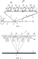
- FIG. 1 is a schematic cross-sectional view of an image forming apparatus 100 according to a first embodiment of the present disclosure.
- the image forming apparatus 100 includes photosensitive drums 1a to 1d, charging devices 2a to 2d, exposure devices 15a to 15d, developing devices 16a to 16d, an intermediate transfer belt 5, a belt support roller 3, a transfer roller 4, and a fixing device 17.
- the photosensitive drums 1a to 1d, the charging devices 2a to 2d, the exposure devices 15a to 15d, and the developing devices 16a to 16d are referred to as an "image forming unit 10" configured to form toner images of respective colors of yellow (Y), cyan (C), magenta (M), and black (K).
- the letter “a” suffixed to the reference signs represents a configuration for forming the yellow image.
- the letter “b” suffixed to the reference signs represents a configuration for forming the cyan image.
- the letter “c” suffixed to the reference signs represents a configuration for forming the magenta image.
- the letter “d” suffixed to the reference signs represents a configuration for forming the black image.
- the intermediate transfer belt 5 is stretched around a plurality of rollers including a drive roller and the belt support roller 3. To the intermediate transfer belt 5, the toner images formed by the image forming unit 10 are transferred.
- the intermediate transfer belt 5 serves as an image bearing member configured to bear and convey the toner images.
- the intermediate transfer belt 5 also serves as an intermediate transfer member, to which the toner images are to be transferred.
- the transfer roller 4 is arranged on a side opposite to the belt support roller 3 with respect to the intermediate transfer belt 5. A nip portion N formed by the transfer roller 4 pressing the intermediate transfer belt 5 is called a "transfer portion".
- the sheet is conveyed to the transfer portion by conveyance rollers.
- the transfer roller 4 is configured to transfer the toner images formed on the intermediate transfer belt 5 onto the sheet at the transfer portion.
- the photosensitive drums 1a, 1b, 1c, and 1d are each rotated in a direction of the arrow A.
- the photosensitive drums 1a, 1b, 1c, and 1d each have a photosensitive layer on a surface thereof.
- the photosensitive drums 1a, 1b, 1c, and 1d serve as photosensitive members.
- the charging devices 2a, 2b, 2c, and 2d are configured to charge the surfaces of the photosensitive drums 1a, 1b, 1c, and 1d, respectively.
- the exposure devices 15a, 15b, 15c, and 15d are configured to expose the charged surfaces of the photosensitive drums 1a, 1b, 1c, and 1d to light, respectively.
- the surfaces of the photosensitive drums 1a, 1b, 1c, and 1d are scanned with laser light emitted from the exposure devices 15a, 15b, 15c, and 15d so that electrostatic latent images are formed on the surfaces of the photosensitive drums 1a, 1b, 1c, and 1d, respectively.
- the developing devices 16a, 16b, 16c, and 16d are configured to develop the electrostatic latent images with toner (developer) to form the toner images of respective colors on the photosensitive drums 1a, 1b, 1c, and 1d, respectively.
- the drive roller of the intermediate transfer belt 5 is rotated to rotate the intermediate transfer belt 5 in a direction of the arrow B.
- the toner images of respective colors formed on the photosensitive drums 1a, 1b, 1c, and 1d are sequentially transferred onto the intermediate transfer belt 5, which is the image bearing member, in an overlapping manner. As a result, a full-color toner image 6 is formed on the intermediate transfer belt 5.
- the intermediate transfer belt 5 is rotated to convey the toner image 6 to the transfer portion.
- the toner image 6 is transferred onto the sheet when passing through the transfer portion.
- the sheet having the toner image 6 transferred thereto is conveyed to the fixing device 17 by a conveyance belt 12.
- the fixing device 17 includes a heater 171.
- the heater 171 is configured to heat the toner image 6 to fix the toner image 6 onto the sheet.
- the sheet is delivered to a tray (not shown) of the image forming apparatus 100. In this manner, image forming processing by the image forming apparatus 100 is ended.
- an optical sensor 7 On a downstream side of the photosensitive drum 1d in a conveyance direction (direction B) of the intermediate transfer belt 5, an optical sensor 7 is arranged.
- the optical sensor 7 is configured to detect pattern images for detecting color misregistration and a test image for detecting an image density, which are formed on the intermediate transfer belt 5.
- a result of detecting the pattern images is used to determine a color misregistration amount, which is used for color misregistration correction.
- a result of detecting the test image is used to determine a correction amount to be used for image density correction.
- the pattern images and the test image are referred to as a "detection image".
- the toner images of respective colors which are transferred from the photosensitive drums 1a to 1d onto the intermediate transfer belt 5, may be shifted in transfer position on the intermediate transfer belt 5. It is known that this is caused by an increase in temperature of the exposure devices 15a to 15d.
- the shift in transfer position causes color misregistration, which changes a hue and a color tone of the full-color image.
- the image forming apparatus 100 is configured to detect the pattern images by the optical sensor 7, and correct the color misregistration detected by a result of the detection.
- the image forming apparatus 100 may vary in density of the image to be formed due to a usage environment (temperature and humidity) and an increase in the number of prints.
- the image forming apparatus 100 is configured to detect the test image, and perform image density correction, in which an image forming condition regarding an image density is controlled based on a result of detecting the test image.
- the image forming condition regarding the image density includes intensities of laser light to be emitted by the exposure devices 15a to 15d, developing biases to be applied to the developing devices 16a to 16d, charging biases to be applied to the charging devices 2a to 2d, or transfer biases to be applied to the transfer roller 4, for example.
- the image forming apparatus 100 may control a plurality of image forming conditions, or control only a particular image forming condition.
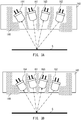
- FIG. 2 is an explanatory view of the optical sensor 7.
- the optical sensor 7 includes two light emitting elements and two light receiving elements.
- the optical sensor 7 includes a first light emitting diode (LED) 701 and a second LED 702 as the light emitting elements.
- the optical sensor 7 includes a first photodiode (PD) 711 and a second PD 712 as the light receiving elements.
- the first LED 701, the second LED 702, the first PD 711, and the second PD 712 are bonded to a predetermined surface (mounting surface) of the same substrate 201 by die bonding and wire bonding.
- Optical axes of light emitted from the first LED 701 and the second LED 702 are orthogonal to the predetermined surface (mounting surface) of the substrate 201.
- optical axes of reflected light received by the first PD 711 and the second PD 712 are also orthogonal to the predetermined surface (mounting surface) of the substrate 201.
- the substrate 201 is a printed circuit board (PCB), for example, but the present disclosure is not limited thereto.
- the first LED 701, the second LED 702, the first PD 711, and the second PD 712 are electrically connected to a power supply circuit (not shown) and a detection circuit (not shown), for example, via the substrate 201.
- the first LED 701 is configured to emit light to an object to be measured (intermediate transfer belt 5 or detection image on the intermediate transfer belt 5).
- the first PD 711 is arranged at a position at which, when the first LED 701 emits light, specularly reflected light from the object to be measured can be received.
- An optical-axis center point P of FIG. 2 indicates a position at which the light emitted from the first LED 701 to the intermediate transfer belt 5 is reflected.
- the first LED 701 and the first PD 711 are arranged such that the light emitted from the first LED 701 is specularly reflected (so that an angle of incidence and an angle of reflection are equal to each other) at the optical-axis center point P, and the reflected light is received by the first PD 711.
- the optical-axis center point P is a detection position of the optical sensor 7.
- the second LED 702 is arranged at a position at which specularly reflected light of light emitted to the intermediate transfer belt 5 is not received by the first PD 711 or the second PD 712.
- the second LED 702 is arranged such that, even when the light emitted from the second LED 702 is specularly reflected at the optical-axis center point P of the intermediate transfer belt 5, the reflected light is not received by the first PD 711 or the second PD 712. Even when the light emitted from the second LED 702 is specularly reflected by the detection image, the specularly reflected light from the detection image is not received by the first PD 711 or the second PD 712.
- the second LED 702 is arranged at a position at which diffused reflected light of the light emitted to the intermediate transfer belt 5 is received by the first PD 711.
- the first LED 701 and the second LED 702 are arranged so as to irradiate the optical-axis center point P, which is the same position.
- the second PD 712 is arranged at a position at which diffused reflected light of light emitted from the first LED 701 to the intermediate transfer belt 5 is received.
- the substrate 201 is mounted to a housing 203.
- the housing 203 has light guide paths for guiding irradiation light so that light emitted from the first LED 701 and the second LED 702 efficiently irradiate the intermediate transfer belt 5.
- the housing 203 also has light guide paths for guiding the reflected light so that the first PD 711 and the second PD 712 efficiently receive the reflected light from the intermediate transfer belt 5.
- the light emitted from the first LED 701 travels in the direction of the optical axis (one-dot broken line in FIG. 2 ), and irradiates the intermediate transfer belt 5, with the light guide path formed in the housing 203.
- the specularly reflected light from the intermediate transfer belt 5 or the detection image travels in the direction of the optical axis (one-dot broken line in FIG. 2 ), and reaches the first PD 711.
- the light emitted from the second LED 702 travels in the direction of the optical axis (one-dot broken line in FIG. 2 ), and irradiates the intermediate transfer belt 5, with the light guide path in the housing 203.
- the first PD 711 is configured to receive diffused reflected light of the light with which the second LED 702 has irradiated the intermediate transfer belt 5.
- the second PD 712 is configured to receive diffused reflected light of the light with which the first LED 701 has irradiated the intermediate transfer belt 5.
- the first LED 701, the second LED 702, the first PD 711, and the second PD 712 are mounted on the same substrate 201, and hence the elements can be mounted substantially in parallel to the intermediate transfer belt 5. Therefore, the shift of the optical axis from the optical-axis center point P can be reduced as compared to the case of forming the elements by bullet elements with lead pins, for example. Further, the first LED 701, the second LED 702, the first PD 711, and the second PD 712 are elements bonded to the substrate 201 by die bonding and wire bonding, and hence can be reduced in element interval. Therefore, the entire size of the optical sensor 7 can be reduced.
- the bullet elements have dimensions of about 5 mm ⁇ about 10 mm ⁇ about 5 mm even without the lead pins. Therefore, a part volume can be significantly reduced, and the optical sensor 7 itself can be downsized.
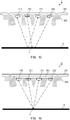
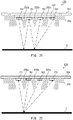
- FIG. 3A and FIG. 3B are explanatory views of the optical sensor including the bullet elements.
- a positional relationship between light emitting elements 161 and 162 and light receiving elements 163 and 164 is achieved by a relationship similar to the case in which the elements are bonded to the substrate by die bonding and wire bonding (irradiation angle, receiving angle), it is required to bring the light emitting element 161 and the light receiving element 163 closer to each other.
- FIG 3B a configuration example in this case is illustrated.
- the light emitting element 161 and the light receiving element 163 have the positional relationship similar to that of FIG.
- the light emitting element 161 and the light receiving element 163 are brought too close to each other.
- a function as a light-shielding wall of a housing 166 provided on a substrate 165 is inhibited. Therefore, in order to prevent the light emitting elements 161 and 162 and the light receiving elements 163 and 164 from interfering with the light-shielding wall, it is required to increase the interval between the elements as in FIG. 3A , but in this case, the optical sensor is increased in size.
- the light emitting elements and the light receiving elements are bonded to the substrate 201 by die bonding and wire bonding.
- the distance between the elements can be reduced.
- the optical sensor 7 can be downsized as compared to the optical sensor including the bullet elements ( FIG. 3A and FIG 3B ).
- the distance between the first LED 701 and the first PD 711 can be reduced, and hence the specularly reflected light of the light emitted to the object to be measured can be detected at an acuter angle than that of the optical sensor including the bullet light emitting elements and the bullet light receiving elements.
- the distance from the optical sensor 7 to the object to be measured is varied, an irradiation area on the object to be measured is hardly varied.
- the intermediate transfer belt 5 is rotating, the distance from the optical sensor 7 to the detection image tends to be varied.
- the optical sensor 7 of the first embodiment even when the distance from the optical sensor 7 to the detection image is varied, the irradiation area is hardly varied, and hence the specularly reflected light from the detection image can be detected with high accuracy. Further, the optical sensor 7 can reduce the distance between the first LED 701 and the first PD 711, and hence design flexibility is also increased. Therefore, according to the optical sensor 7, the first LED 701, the second LED 702, the first PD 711, and the second PD 712 can be arranged in a positional relationship that is suitable for detecting the specularly reflected light and the diffused reflected light from the object to be measured. In particular, in the optical sensor 7 in which the light emitting elements are shared or the light receiving elements are shared, the specularly reflected light and the diffused reflected light from the detection image can be detected more accurately than in the related-art optical sensor including the bullet elements.
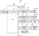
- FIG. 4 is an exemplary diagram of an example of a configuration of a controller configured to control the image forming apparatus 100.
- a controller 40 includes a central processing unit (CPU) 109, a read-only memory (ROM) 111, and an image forming controller 101.
- the CPU 109 includes an A/D converter 110.
- the image forming controller 101 includes an exposure device controller 112, a developing device controller 113, a photosensitive drum controller 114, and an intermediate transfer belt driver 115.
- the exposure device controller 112 is configured to control intensities of laser light emitted from light sources included in the exposure devices 15a to 15d.
- the developing device controller 113 is configured to control motors for rotating developing rollers included in the developing devices 16a to 16d.
- the photosensitive drum controller 114 is configured to control motors for rotating the photosensitive drums 1a to 1d.
- the intermediate transfer belt driver 115 is configured to control a motor for rotating the intermediate transfer belt 5.
- the CPU 109 is configured to control the image forming apparatus 100 by executing a computer program stored in the ROM 111.
- the ROM 111 has stored therein, in addition to the computer program, pattern image data to be used to form the pattern images for the color misregistration detection, which are to be described later, and test image data to be used for forming the test image for the image density detection.
- the controller 40 may be implemented not only by executing the computer program, but also by a discrete part or a one-chip semiconductor product.
- the one-chip semiconductor product includes a micro-processing unit (MPU), an application specific integrated circuit (ASIC), or a system-on-a-chip (SOC), for example.
- MPU micro-processing unit
- ASIC application specific integrated circuit
- SOC system-on-a-chip
- the CPU 109 is configured to control the optical sensor 7 to cause the first LED 701 and the second LED 702 to independently emit light (be lit).
- the optical sensor 7 is configured to receive reflected light from the intermediate transfer belt 5 or the detection image formed on the intermediate transfer belt 5 by the first PD 711 and the second PD 712.
- the first PD 711 and the second PD 712 are configured to output, as a detection result, an analog signal obtained by converting the received reflected light into a voltage.
- the CPU 109 is configured to acquire analog signals output from the first PD 711 and the second PD 712 through the A/D converter 110.
- the CPU 109 is configured to store, in a memory (not shown), digital signals into which the analog signals are converted by the A/D converter 110.
- the CPU 109 is configured to control the exposure devices 15a to 15d, the developing devices 16a to 16d, and the photosensitive drums 1a to 1d by the image forming controller 101 to form the detection image on the intermediate transfer belt 5.
- the CPU 109 is configured to cause the first LED 701 and the second LED 702 of the optical sensor 7 to be lit.
- the first LED 701 and the second LED 702 are configured to irradiate the surface (front surface) of the intermediate transfer belt 5, on which the detection image is to be formed, and the detection image formed on the intermediate transfer belt 5.
- the first PD 711 and the second PD 712 are configured to receive reflected light from the front surface of the intermediate transfer belt 5 and the detection image formed on the intermediate transfer belt 5 to output an analog signal corresponding to the reflected light.
- the CPU 109 is configured to detect the color misregistration amount and the image density in accordance with the analog signals output from the first PD 711 and the second PD 712 to perform the color misregistration correction and the image density correction.
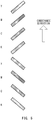
- FIG. 5 is an explanatory diagram of first pattern images for the color misregistration detection.
- the first pattern images include color patterns of yellow, which is a reference color, and color patterns of other colors (magenta, cyan, and black).
- the color patterns are images formed to be inclined at a predetermined angle (for example, 45°) with respect to the conveyance direction of the intermediate transfer belt 5.
- Two pattern images of the same colors are formed.
- the pattern images of the same colors are formed to be inclined in different directions with respect to the conveyance direction of the intermediate transfer belt 5.
- the first pattern images are used in the case where the first PD 711 receives the specularly reflected light of the light emitted from the first LED 701.
- the color misregistration amount is detected with the use of the first pattern images.
- an amount of the specularly reflected light from the front surface of the intermediate transfer belt 5 becomes larger than an amount of specularly reflected light from the first pattern images.
- an analog signal value corresponding to a result of receiving the reflected light from a region (front surface of the intermediate transfer belt 5) in which the first pattern images are not formed becomes higher than an analog signal value corresponding to a result of receiving the reflected light from the first pattern images.
- FIG. 6 is a graph for showing an example of an analog signal in a case where reflected light from the first pattern images is detected by the first LED 701 and the first PD 711.
- An analog signal value of the first PD 711 obtained when reflected light from a color pattern is received is lower than an analog signal value of the first PD 711 obtained when the reflected light from the front surface of the intermediate transfer belt 5 is received.
- the CPU 109 is configured to convert the analog signal into a binary signal indicating a first level or a second level based on a first threshold value.
- the converted signal corresponds to a result of comparison between the analog signal value ( FIG. 6 ) and the first threshold value.
- the CPU 109 determines the first threshold value based on an analog signal value obtained when the specularly reflected light from the front surface of the intermediate transfer belt 5 of the light emitted from the first LED 701 is received by the first PD 711. Then, the CPU 109 detects a color misregistration amount of the color pattern of the first pattern images based on the binary signal described above.
- the color misregistration correction is a known technology, and a detailed description thereof is omitted here.
- FIG. 7A and FIG. 7B are explanatory diagrams of second pattern images for the color misregistration detection.
- the second pattern images include color patterns of yellow, which is a reference color, and color patterns of other colors (magenta, cyan, and black). It should be noted, however, that the color patterns of black of the second pattern images are formed to be superimposed on the color patterns of magenta.
- the second pattern images are used when diffused reflected light of the light emitted from the second LED 702 is received by the first PD 711. In other words, when the amount of the reflected light from the intermediate transfer belt 5 is not the predetermined amount or more, a color misregistration amount is detected with the use of the second pattern images. In other words, when the amount of reflected light from the intermediate transfer belt 5 is less than the predetermined amount, the color misregistration amount is detected with the use of the second pattern images.
- FIG. 8 is a graph for showing an example of an analog signal obtained when the reflected light from the first pattern images is detected by the first LED 701 and the first PD 711 under a state in which the gloss of the intermediate transfer belt 5 is reduced.
- the CPU 109 may not detect the color misregistration amount from the binary signal with high accuracy.
- the image forming apparatus 100 detects the color misregistration amount with the use of the second pattern images.
- the optical sensor 7 causes the second LED 702 to emit light, and the first PD 711 receives diffused reflected light from the second pattern images.
- FIG. 9 is a graph for showing an example of an analog signal obtained when reflected light from the second pattern images is detected by the second LED 702 and the first PD 711.
- the second pattern images are different from the first pattern images.
- the color patterns of black are superimposed on the color patterns of magenta.
- the light emitted from the second LED 702 is absorbed by a black toner. Therefore, a difference between the amount of diffused reflected light from the color patterns of only black and the amount of diffused reflected light from the intermediate transfer belt 5 becomes extremely smaller.
- a pattern formed with the use of a magenta toner is exposed from a gap of patterns formed at an interval with the use of the black toner. This is called a "composite pattern".
- FIG. 7B A cross-sectional view of the composite pattern is illustrated in FIG. 7B .
- FIG. 9 A result of detecting the second pattern images including the composite patterns is shown in FIG. 9 .
- An analog signal value corresponding to diffused reflected light from the composite pattern is a value corresponding to diffused reflected light from a region of the composite pattern formed with the use of the magenta toner.
- the interval between the patterns of the black toner is determined in advance, and hence the CPU 109 can determine a color misregistration amount of the color patterns of black based on a relative position between the region of the composite pattern formed with the use of the magenta toner and the reference color patterns using a yellow toner.
- the CPU 109 is configured to convert the analog signal ( FIG. 9 ) into a binary signal indicating the first level or the second level based on a second threshold value.
- the converted signal corresponds to a result of comparison between the analog signal value ( FIG. 9 ) and the second threshold value.
- the CPU 109 determines the second threshold value based on an analog signal value obtained when the diffused reflected light from the front surface of the intermediate transfer belt 5 of the light emitted from the second LED 702 is received by the first PD 711. Then, the CPU 109 detects a color misregistration amount of the color pattern of the second pattern images based on the binary signal described above.
- the color misregistration correction using a composite pattern is a known technology, and a detailed description thereof is omitted here.
- the color misregistration amount of the image is detected with the use of the above-mentioned pattern images (first pattern images and second pattern images).
- the CPU 109 detects positions of the color patterns of respective colors to calculate relative positions of the pattern images of other colors with respect to the pattern images of the reference color (yellow).
- the CPU 109 determines the color misregistration amounts of respective colors based on differences between the calculated relative positions and a target relative position.
- the CPU 109 controls timings of writing by the exposure devices 15a to 15d based on the determined color misregistration amounts to perform the color misregistration correction.
- the CPU 109 may correct image data based on the detected color misregistration so that the color misregistration amounts of the image to be formed by the image forming unit 10 are suppressed, for example.
- the reference color is not limited to yellow, and may be magenta or cyan.
- FIG. 10A and FIG. 10B are explanatory diagrams of test images for the image density detection.
- FIG. 10A an example of a first test image for the image density detection to be detected with the specularly reflected light is illustrated.
- FIG. 10B an example of a second test image for the image density detection to be detected with diffused reflected light is illustrated.
- the first test image is used when the specularly reflected light of the light emitted from the first LED 701 is received by the first PD 711.
- the first test image is used in detecting an image density of black, in particular.
- the black toner absorbs light, and hence an amount of diffused reflected light from a test image of black is extremely small. Therefore, when a density of an image formed by the black toner is to be detected, the CPU 109 detects specularly reflected light from the test image of black.
- the first test image is formed of a gradation pattern of four image densities: 70%, 50%, 30%, and 10%.
- the image forming unit 10 forms the first test image based on an image signal value of the test image data. The image signal value of the test image data is determined in advance.
- the first test image formed on the intermediate transfer belt 5 is read by the optical sensor 7.
- the analog signal output from the first PD 711 is converted to the digital signal by the A/D converter 110.
- the CPU 109 controls the image forming condition for the image density based on a difference between the digital signal value and a target value. For example, the CPU 109 controls an intensity of laser light emitted from the exposure device 15d by the image forming controller 101 to adjust the image density of black.
- FIG. 11 is a graph for showing an example of an analog signal obtained when reflected light from the first test image is detected by the first LED 701 and the first PD 711.
- the image of the density of 70% which is the highest density of the first test image, is reduced in the amount of specularly reflected light because a toner adhesion amount is large in addition to the fact that the light is absorbed by the black toner. Therefore, the analog signal value output by the optical sensor 7 (first PD 711) is reduced.
- the image of the density of 10% which is the lowest density of the first test image, is reduced in the amount of light absorbed by the black toner as compared to the case of the density of 70%, and the toner adhesion amount is reduced, with the result that the amount of the specularly reflected light is increased. Therefore, the analog signal value output by the optical sensor 7 (first PD 711) is increased.
- the second test image is used when diffused reflected light of light emitted from the first LED 701 is received by the second PD 712.
- the second test image is used in detecting image densities of chromatic colors, such as yellow, magenta, and cyan, in particular. Image densities for yellow, magenta, and cyan are detected with the use of diffused reflected light.
- the second test image is formed of a gradation pattern of four densities: 70%, 50%, 30%, and 10%.
- FIG. 10B a test image of yellow is illustrated.
- the second test images of the colors: yellow, magenta, and cyan are formed on the intermediate transfer belt 5.
- the second test image formed on the intermediate transfer belt 5 is read by the optical sensor 7.
- the analog signal output from the second PD 712 is converted to the digital signal by the A/D converter 110.
- the CPU 109 controls the image forming condition for the image density based on a difference between the digital signal value and a target value. In this manner, the CPU 109 adjusts the image densities of yellow, magenta, and cyan.
- FIG. 12 is a graph for showing an example of an analog signal obtained when reflected light from the second test image is detected by the first LED 701 and the second PD 712.
- An analog signal of the second test image for yellow is illustrated here.
- the image of the density of 70% which is the highest density of the second test image, is increased in the amount of diffused reflected light because a toner adhesion amount is large in addition to the fact that the light is reflected by the yellow toner. Therefore, the analog signal value output by the optical sensor 7 (second PD 712) is increased.
- the image of the density of 10%, which is the lowest density of the second test image is reduced in the amount of light reflected by the yellow toner as compared to the case of the density of 70%, and the amount of the diffused reflected light is reduced. Therefore, the analog signal value output by the optical sensor 7 (second PD 712) is reduced.
- Analog signals obtained with the second test images of magenta and cyan exhibit similar tendencies.
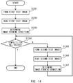
- FIG. 13 is a flow chart for illustrating processing of detecting the color misregistration amounts in the first embodiment.
- the CPU 109 first detects the amount of light reflected on the front surface of the intermediate transfer belt 5 by the optical sensor 7 (Step S1201).
- the CPU 109 causes the first LED 701 to emit light.
- An image is not formed on the intermediate transfer belt 5 at this time, and hence the light from the first LED 701 irradiates the front surface of the intermediate transfer belt 5.
- the first PD 711 receives the specularly reflected light from the front surface of the intermediate transfer belt 5 to output an analog signal corresponding to the amount of specularly reflected light.
- the CPU 109 acquires the analog signal from the first PD 711 to detect the amount of light reflected by the front surface of the intermediate transfer belt 5.
- the CPU 109 determines whether the acquired amount of light reflected by the front surface of the intermediate transfer belt 5 is the predetermined amount or more (Step S1202). Through this processing, the CPU 109 determines whether the gloss of the front surface of the intermediate transfer belt 5 is high.
- Step S1202 When the amount of light reflected by the front surface of the intermediate transfer belt 5 is the predetermined amount or more (Step S1202: Y), the CPU 109 determines that the gloss of the front surface of the intermediate transfer belt 5 is not reduced. In this case, the CPU 109 detects the color misregistration amount with the use of the first pattern images. In other words, the CPU 109 transfers pattern image data P1 to the image forming controller 101, and controls the image forming controller 101 to form the first pattern images on the intermediate transfer belt 5 (Step S1203). The CPU 109 causes the first LED 701 to emit light, and reads the first pattern images formed on the intermediate transfer belt 5 by the first PD 711 (Step S1204).
- Step S1204 the CPU 109 acquires the analog signal output from the first PD 711.
- the CPU 109 calculates the color misregistration amount from the result of detecting the first pattern images of respective colors of yellow, magenta, cyan, and black (Step S1207).
- Step S1202 When the amount of light reflected by the front surface of the intermediate transfer belt 5 is less than the predetermined amount (Step S1202: N), the CPU 109 determines that the gloss of the front surface of the intermediate transfer belt 5 is reduced. In this case, the CPU 109 detects the color misregistration amount with the use of the second pattern images. In other words, the CPU 109 transfers pattern image data P2 to the image forming controller 101, and controls the image forming controller 101 to form the second pattern images on the intermediate transfer belt 5 (Step S1205). The CPU 109 causes the second LED 702 to emit light, and reads the second pattern images formed on the intermediate transfer belt 5 by the first PD 711 (Step S1206).
- Step S1206 the CPU 109 acquires the analog signal output from the first PD 711. Then, the CPU 109 causes the processing to proceed to Step S1207.
- the CPU 109 calculates the color misregistration amount based on the result of detecting the second pattern images of respective colors of yellow, magenta, cyan, and black (Step S1207). After the processing of Step S1207 is complete, the CPU 109 ends the processing of detecting the color misregistration amount.
- the CPU 109 stores the calculated color misregistration amount in the memory (not shown).
- the CPU 109 reads the color misregistration amount from the memory, and corrects image forming positions of the images to be formed based on the image data in accordance with the color misregistration amount.
- the CPU 109 uses the pattern images (first pattern images and second pattern images) for the color misregistration detection corresponding to the result of detecting the gloss of the intermediate transfer belt 5 to acquire the color misregistration amount with an optimal combination of a light emitter and a light receiver. Therefore, the CPU 109 can detect an accurate color misregistration amount to perform accurate color misregistration correction.
- FIG. 14 is a flow chart for illustrating image density detection processing in the first embodiment.
- a description is given of a case in which the image density detection for the chromatic colors is performed after the image density detection for black, but the order may be reversed.
- the CPU 109 transfers test image data TK to the image forming controller 101, and controls the image forming controller 101 to form the test image of black (first test image) on the intermediate transfer belt 5 (Step S1301).
- the CPU 109 causes the first LED 701 to emit light, and acquires the analog signal from the first PD 711, which has received the specularly reflected light, to read the test image of black (Step S1302).
- the CPU 109 converts a level of the analog signal corresponding to the read test image of black into a digital signal value by the A/D converter 110.
- the CPU 109 determines the image forming condition for the image density based on the digital signal value (Step S1303).
- Step S1303 the CPU 109 determines, as the image forming condition regarding the image density for black, a correction amount of an intensity of laser light of the exposure device 15d, and stores the correction amount in the memory (not shown).
- the CPU 109 reads the correction amount from the memory, and controls the density of the black image to be formed by the image forming unit 10 in accordance with the correction amount.
- the CPU 109 determines whether the image density detection processing has been performed for all colors of yellow, magenta, and cyan (Step S1304).
- the CPU 109 When the image density detection has not been performed for all colors (Step S1304: N), the CPU 109 first performs the image density detection for yellow. In other words, the CPU 109 transfers test image data TY to the image forming controller 101, and controls the image forming controller 101 to form the test image of yellow (second test image) on the intermediate transfer belt 5 (Step S1305). The CPU 109 causes the first LED 701 to emit light, and acquires the analog signal from the second PD 712, which has received the diffused reflected light, to read the test image of yellow (Step S1306). The CPU 109 converts a level of the analog signal corresponding to the read test image of yellow into a digital signal value by the A/D converter 110.
- the CPU 109 determines the image forming condition for the image density based on the digital signal value (Step S1307). In Step S1307, the CPU 109 determines, as the image forming condition regarding the image density for yellow, a correction amount of an intensity of laser light of the exposure device 15a, and stores the correction amount in the memory (not shown). When the yellow image is to be formed, the CPU 109 reads the correction amount from the memory, and controls the density of the yellow image to be formed by the image forming unit 10 in accordance with the correction amount.
- the CPU 109 repeatedly performs the processing of Step S1305 to Step S1307 until the image density detection processing is ended for all colors.
- the CPU 109 ends the image density detection processing.
- the CPU 109 uses the test image (first test image, second test image) for the image density detection corresponding to the color to be detected to acquire the image density with an optimal combination of a light emitter and a light receiver. Therefore, the CPU 109 can detect a correction amount of an accurate image density to perform accurate image density correction.
- the image forming apparatus 100 includes the optical sensor 7 having a plurality of light emitting elements and light receiving elements bonded on the same substrate 201 by die bonding and wire bonding. Therefore, the size and the cost of the optical sensor 7 itself can be reduced.
- the image forming apparatus 100 uses the optical sensor 7 in both of a specularly reflected light method and a diffused reflected light method. Moreover, the image forming apparatus 100 separately prepares the detection image for use in the specularly reflected light method and the detection image for use in the diffused reflected light method.
- the image forming apparatus 100 can achieve the detection of the pattern images suitable for the state of the intermediate transfer belt 5 by combining the first LED 701, the second LED 702, and the first PD 711 in an optimal manner. Moreover, in the image density detection processing, the image forming apparatus 100 can achieve the detection of the test image suitable for the color of the test image by combining the first LED 701, the first PD 711, and the second PD 712 in an optimal manner.
- the first LED 701, the second LED 702, the first PD 711, and the second PD 712 are bonded to the substrate 201 by die bonding and wire bonding, and hence the first LED 701 and the first PD 711 used in the specularly reflected light method are positioned accurately. Meanwhile, positioning among other elements can be performed with a margin. Therefore, an assembly operation of the optical sensor 7 becomes easier than in the related art.
- the first LED 701 or the second LED 702 and the first PD 711 are combined.
- the same element (first PD 711) is used on the light receiving side.
- the position of the light receiving element (first PD 711) is fixed, and hence detection accuracy of the color misregistration amount is increased as compared to the case in which the first pattern images and the second pattern images are detected by different light receiving elements.
- the first LED 701 and the first PD 711 or the second PD 712 are combined.
- the same element (first LED 701) is used on the light emitting side. Therefore, a light emission amount is constant for the case where the test image of black is measured and for a case where a test image of a chromatic color is measured, and detection accuracy of the image density is increased.
- FIG. 15 is an explanatory diagram of the optical sensor 7 in the case where the mounting accuracy of each part is reduced.
- the optical sensor 7 cannot detect the detection image with the optical-axis center point P being the detection position. Therefore, it is preferred to increase the mounting accuracy of the first LED 701, the second LED 702, the first PD 711, and the second PD 712.
- FIG. 16 is a schematic view of a main part of an optical sensor 14.
- the optical sensor 14 includes a first LED 721 and a second LED 722 as the light emitting elements, and a first PD 731 and a second PD 732 as the light receiving elements.
- the first LED 721, the second LED 722, the first PD 731, and the second PD 732 are formed as semiconductor elements on the same semiconductor substrate 141.
- the surface on which the first LED 721, the second LED 722, the first PD 731, and the second PD 732 are formed is referred to as a "processing surface".
- the optical axis of the irradiation light from the first LED 721 and the second LED 722 is orthogonal to the processing surface of the semiconductor substrate 141.
- optical axis of reflected light received by the first PD 731 and the second PD 732 is also orthogonal to the processing surface of the semiconductor substrate 141.
- the semiconductor substrate 141 is fixed on the substrate 201 with the use of an adhesive, for example, an epoxy resin.
- the substrate 201 is mounted to the housing 203.
- the housing 203 has light guide paths for guiding the irradiation light so that light emitted from the first LED 721 and the second LED 722 efficiently irradiate the intermediate transfer belt 5.
- the housing 203 also has light guide paths for guiding the reflected light so that the first PD 731 and the second PD 732 efficiently receive the reflected light from the intermediate transfer belt 5.
- the light emitted from the first LED 721 travels in the direction of the optical axis (one-dot broken line in FIG. 16 ), and irradiates the intermediate transfer belt 5, with the light guide path formed in the housing 203.
- the specularly reflected light from the intermediate transfer belt 5 or the detection image travels in the direction of the optical axis (one-dot broken line in FIG. 16 ), and reaches the first PD 731.
- the light emitted from the second LED 722 travels in the direction of the optical axis (one-dot broken line in FIG. 16 ), and irradiates the intermediate transfer belt 5, with the light guide path in the housing 203.
- the first PD 731 is configured to receive diffused reflected light of the light with which the second LED 722 has irradiated the intermediate transfer belt 5.
- the second PD 732 is configured to receive diffused reflected light of the light emitted from the first LED 721 to irradiate the intermediate transfer belt 5.
- the elements are formed on the semiconductor substrate 141, and hence the positional accuracy of each element can be ensured at a high level.
- the optical sensor 14 can easily focus the optical axis of each element on the optical-axis center point P. As a result, the detection accuracy of the detection image is increased further than that attained by the optical sensor 7 directly bonded to the substrate.
- the light emitter and the light receiver are formed on the semiconductor substrate 141, and hence the distance between the elements can be reduced.
- the optical sensor 14 can be downsized as compared to the optical sensor including the bullet elements ( FIG. 3A and FIG. 3B ).
- the distance between the first LED 721 and the first PD 731 can be reduced, and hence the specularly reflected light of the light emitted to the object to be measured can be detected at an acuter angle than that of the optical sensor including the bullet light emitting elements and the bullet light receiving elements.
- the optical sensor 14 of the first embodiment even when the distance from the optical sensor 14 to the detection image is varied, the irradiation area is hardly varied, and hence the specularly reflected light from the detection image can be detected with high accuracy. Further, the optical sensor 14 can reduce the distance between the first LED 721 and the first PD 731, and hence design flexibility is also increased.
- the first LED 721, the second LED 722, the first PD 731, and the second PD 732 can be arranged in a positional relationship that is suitable for detecting the specularly reflected light and the diffused reflected light from the object to be measured.
- the specularly reflected light and the diffused reflected light from the detection image can be detected more accurately than in the related-art optical sensor including the bullet elements.
- a configuration of an image forming apparatus according to a second embodiment of the present disclosure is the same as the configuration of the image forming apparatus 100 according to the first embodiment exemplified in FIG. 1 , and hence a description thereof is omitted.
- FIG. 17 is a schematic view of a main part of the optical sensor 7.
- the optical sensor 7 according to the second embodiment is different from the optical sensor 7 according to the first embodiment illustrated in FIG. 2 in array of elements.
- light emitting elements and light receiving elements are arranged on the substrate 201 in the following order: the first LED 701, the first PD 711, the second PD 712, and the second LED 702.
- the first PD 711 and the second PD 712 are located between the first LED 701 and the second LED 702.
- the optical sensor 7 includes a housing 203, in which light-shielding walls 202a, 202b, and 202c are formed.
- a positional relationship between the first LED 701 and the first PD 711 is a positional relationship in which, when the first LED 701 emits light, the first PD 711 can receive specularly reflected light from the object to be measured.
- an angle of incidence of the light emitted from the first LED 701 is equal to an angle of reflection of reflected light received by the first PD 711.
- the angle of incidence of the light from the first LED 701 is 7°, for example, and the angle of reflection of the first PD 711 is 7°, for example.
- a positional relationship between the first PD 711 and the second LED 702 is a positional relationship in which, when the second LED 702 emits light, the first PD 711 can receive diffused reflected light from the object to be measured.
- an angle of incidence of the light emitted from the second LED 702 is different from an angle of reflection of reflected light received by the first PD 711.
- the angle of incidence of the light from the second LED 702 is 30°, for example, and the angle of reflection of the first PD 711 is 7°, for example.
- a positional relationship between the second LED 702 and the second PD 712 is a positional relationship in which, when the second LED 702 emits light, the second PD 712 can receive other diffused reflected light from the object to be measured.
- an angle of incidence of the light emitted from the second LED 702 is different from an angle of reflection of reflected light received by the second PD 712.
- an angle of reflection of the reflected light received by the first PD 711 is also different from the angle of reflection of the reflected light received by the second PD 712.
- the angle of incidence of the light from the second LED 702 is 30°, for example, and the angle of reflection of the second PD 712 is -7°, for example.
- the positional relationship between the second LED 702 and each of the first PD 711 and the second PD 712 is determined such that, even when the light from the second LED 702 is reflected by the object to be measured, the specularly reflected light from the object to be measured is not received by the first PD 711 or the second PD 712.
- the substrate 201 is mounted to the housing 203.
- the light-shielding walls 202a, 202b, and 202c are located among the light emitting elements and the light receiving elements.
- the light-shielding wall 202a is located between the first LED 701 and the first PD 711
- the light-shielding wall 202b is located between the first PD 711 and the second PD 712
- the light-shielding wall 202c is located between the second PD 712 and the second LED 702.
- the light-shielding wall 202a prevents the light emitted from the first LED 701 from being directly received by the first PD 711 and the second PD 712.
- the light-shielding wall 202c prevents the light emitted from the second LED 702 from being directly received by the second PD 712 and the first PD 711.
- the light-shielding wall 202b prevents light diffused by the first PD 711 from being received by the second PD 712, and prevents light diffused by the second PD 712 from being received by the first PD 711.
- the housing 203, and the light-shielding wall 202a and the light-shielding wall 202c guide the irradiation light so that the intermediate transfer belt 5 is irradiated efficiently with the light emitted from the first LED 701 and the second LED 702.
- the light-shielding walls 202a, 202b, and 202c function as guides for reflected light from the intermediate transfer belt 5 to be efficiently received by the first PD 711 and the second PD 712.
- the first LED 701, the second LED 702, the first PD 711, and the second PD 712 are mounted on the same substrate 201, and hence the elements can be mounted substantially in parallel to the intermediate transfer belt 5.
- the shift of the optical axis can be reduced as compared to the optical sensor including bullet elements with lead pins, for example.
- the first LED 701, the second LED 702, the first PD 711, and the second PD 712 are elements bonded to the substrate 201 by die bonding and wire bonding, and hence can be reduced in element interval as compared to the bullet elements. Therefore, the entire size of the optical sensor 7 can be reduced.
- the elements included in the optical sensor 7 according to the second embodiment are arrayed on the substrate 201 in the following order: the first LED 701, the first PD 711, the second PD 712, and the second LED 702.
- a plurality of light emitting elements and a plurality of light receiving elements are arrayed so as not to sandwich one light receiving element between two light emitting elements. The reason of such array is described.
- FIG. 18A and FIG. 18B are explanatory diagrams of an LED used for the light emitting elements (first LED 701 and second LED 702) in the second embodiment.
- an LED 1700 has a double heterostructure in which a p-type cladding layer 1702, a light emitting layer 1703, and an n-type cladding layer 1704 are laminated on an electrode 1701. On the n-type cladding layer 1704, electrodes 1705 and 1706 are provided.
- the light emitting layer 1703 outputs light in all directions.
- FIG. 18B a light emission directional pattern of the LED 1700 is exemplified.
- the LED 1700 outputs light also in edge-on directions of 90° and -90°, for example.
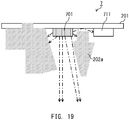
- FIG. 19 is an enlarged view of a periphery of the first LED 701 and the first PD 711 of the optical sensor 7.
- the light-shielding wall 202a configured to prevent the light emitted from the first LED 701 from directly reaching the first PD 711 is provided.
- a gap may be formed between the light-shielding wall 202a, which is formed in the housing 203, and the substrate 201.
- the first PD 711 is arranged so as to receive the specularly reflected light from the object to be measured when the first LED 701 emits light.
- the first PD 711 receives, in addition to the specularly reflected light from the object to be measured, stray light leaking out of the gap as illustrated in FIG. 19 .
- the first PD 711 cannot detect the specularly reflected light from the object to be measured with high accuracy.
- accurate color misregistration detection and image density detection are hindered.
- the second PD 712 is arranged so as to receive diffused reflected light from the object to be measured when the second LED 702 emits light.
- the light-shielding wall 202c configured to prevent the light emitted from the second LED 702 from directly reaching the second PD 712 is provided.
- the second PD 712 cannot detect the diffused reflected light from the object to be measured with high accuracy. In other words, with the second PD 712 receiving the stray light leaking out of the gap between the light-shielding wall 202c and the substrate 201, accurate color misregistration detection and image density detection are hindered.
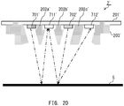
- FIG. 20 a comparative example of an optical sensor 7', in which a gap is easily formed in the light-shielding walls, is illustrated. Arrangement of elements of the optical sensor 7' is different from the arrangement of the elements of the optical sensor 7 of FIG. 17 .
- elements are arrayed on a substrate 201' in the following order: a first LED 701', a first PD 711', a second LED 702', and a second PD 712'. Further, the optical sensor 7' illustrated in FIG.
- the 20 has a light-shielding wall 202a' between the first LED 701' and the first PD 711', a light-shielding wall 202b' between the first PD 711' and the second LED 702', and a light-shielding wall 202c' between the second LED 702' and the second PD 712'.
- temperatures of the first PD 711' and its surroundings are increased not only when the first LED 701' emits light but also when the second LED 702' emits light.
- a distance between the first LED 701' and the second LED 702' which correspond to two heat sources, is shorter than in the optical sensor 7 illustrated in FIG.
- a gap is easily formed between the substrate 201' and the light-shielding wall 202a', and further, a gap is easily formed between the substrate 201' and the light-shielding wall 202b'.
- the optical sensor 7' illustrated in FIG. 20 the gaps out of which stray light leaks are easily formed in the light-shielding walls 202a' and 202b', and the first PD 711' cannot detect reflected light from the detection image with high accuracy.
- the first PD 711' is affected by the stray light leaking out of the gaps in the light-shielding walls 202a' and 202b' both when the first LED 701' emits light and when the second LED 702' emits light. Therefore, with the optical sensor 7' illustrated in FIG. 20 , the first PD 711' cannot detect the reflected light from the detection image with high accuracy also when the second LED 702' emits light. Further, when the temperature around the second LED 702' is increased, stray light may leak out of the gaps in the light-shielding wall 202b' and the light-shielding wall 202c'.
- both of the first PD 711' and the second PD 712' cannot detect reflected light from the detection image with high accuracy.
- the elements are arrayed on the substrate 201 in the following order: the first LED 701, the first PD 711, the second PD 712, and the second LED 702.
- the distance from the first LED 701 to the second LED 702 can be made farther than in the optical sensor 7' illustrated in FIG. 20 without increasing the size.
- the temperature of the region between the first LED 701 and the second LED 702 is less likely to be increased.
- the distance from the light-shielding wall 202c to the first LED 701 is longer than in the optical sensor 7' illustrated in FIG. 20 , and hence the gap is less likely be formed between the light-shielding wall 202c and the substrate 201 even when the first LED 701 emits light.
- the distance from the light-shielding wall 202a to the second LED 702 is longer than in the optical sensor 7' illustrated in FIG. 20 , and hence the gap is less likely to be formed between the light-shielding wall 202a and the substrate 201 even when the second LED 702 emits light. Therefore, according to the optical sensor 7 illustrated in FIG. 17 , the stray light, which causes the reduction in detection accuracy of the optical sensor 7, can be prevented from being generated. Further, according to the optical sensor 7, with the stray light being prevented from being generated, the reflected light from the detection image can be detected with high accuracy.
- a configuration of a controller configured to control an operation of the image forming apparatus 100 according to the second embodiment is the same as the configuration of the controller of the image forming apparatus 100 according to the first embodiment exemplified in FIG. 4 , and hence a description thereof is omitted.
- the image forming apparatus 100 according to the second embodiment can also perform color misregistration correction processing ( FIG. 13 ) and image density correction processing ( FIG. 14 ) with the use of pattern images ( FIG. 5 , FIG. 7A and FIG. 7B ) and a test image ( FIG. 10A, FIG. 10B ) similar to those of the image forming apparatus 100 according to the first embodiment.
- the image forming apparatus 100 according to the second embodiment provides actions and effects similar to those of the first embodiment. Further, the image forming apparatus 100 according to the second embodiment can suppress the effect of the stray light accompanying the increase in temperature and detect the reflected light from the detection image with high accuracy with the characteristic array of the elements in the optical sensor 7. Therefore, color misregistration correction and image density correction with higher accuracy than in the related art are achieved.
- the optical sensor 7 according to the second embodiment of FIG. 17 be increased in mounting accuracy of the first LED 701, the second LED 702, the first PD 711, and the second PD 712.
- FIG. 21 is a schematic view of a main part of an optical sensor 140 including a semiconductor substrate having formed thereon light emitting elements and light receiving elements.
- the optical sensor 140 includes a first LED 741 and a second LED 742 as the light emitting elements, and a first PD 751 and a second PD 752 as the light receiving elements.
- the first LED 741, the second LED 742, the first PD 751, and the second PD 752 are formed as semiconductor elements on the same semiconductor substrate 142.
- the surface on which the first LED 741, the second LED 742, the first PD 751, and the second PD 752 are formed is referred to as a "processing surface".
- the optical axis of the irradiation light from the first LED 741 and the second LED 742 is orthogonal to the processing surface of the semiconductor substrate 142. Further, the optical axis of reflected light received by the first PD 751 and the second PD 752 is also orthogonal to the processing surface of the semiconductor substrate 142.
- the semiconductor substrate 142 is fixed on the substrate 201 with the use of an adhesive, for example, an epoxy resin.
- the substrate 201 is mounted to the housing 203.
- the housing 203 has light guide paths for guiding the irradiation light so that light emitted from the first LED 741 and the second LED 742 efficiently irradiate the intermediate transfer belt 5.
- the housing 203 also has light guide paths for guiding the reflected light so that the first PD 751 and the second PD 752 efficiently receive the reflected light from the intermediate transfer belt 5.
- the light emitted from the first LED 741 travels in the direction of the optical axis (one-dot broken line in FIG. 21 ), and irradiates the intermediate transfer belt 5, with the light guide path formed in the housing 203.
- the specularly reflected light from the intermediate transfer belt 5 or the detection image travels in the direction of the optical axis (one-dot broken line in FIG. 21 ), and reaches the first PD 751.
- the light emitted from the second LED 742 travels in the direction of the optical axis (one-dot broken line in FIG. 21 ), and irradiates the intermediate transfer belt 5, with the light guide path in the housing 203.
- the first PD 751 and the second PD 752 are configured to receive diffused reflected light of the light emitted from the second LED 742 to irradiate the intermediate transfer belt 5.
- the elements are formed on the semiconductor substrate 142, and hence the positional accuracy of each element can be ensured at high level.
- the optical sensor 140 can easily focus the optical axis of each element on the optical-axis center point P.
- the accuracy of detecting the detection image is increased further than that of the optical sensor 7 including the elements bonded to the substrate by die bonding and wire bonding.
- the two light receiving elements are arranged between the two light emitting elements, and hence the gap is prevented from being formed between the substrate and each of the light-shielding walls located between the light emitting elements and the light receiving elements due to the heat from the light emitting elements.
- an optical sensor 210 of FIG. 22 in which two light emitting elements are arranged between two light receiving elements, is described.
- the light-shielding walls 202a, 202b, and 202c are formed in the housing 203.
- the present disclosure is also applicable to a case in which the light-shielding walls 202a, 202b, and 202c are members different from the housing 203.
- the light-shielding walls 202a, 202b, and 202c are members different from the housing 203, through arrangement of a plurality of light receiving elements between a light emitting element and another light emitting element, a gap can be prevented from being formed between the housing 203 and each of the light-shielding walls 202a, 202b, and 202c.
- FIG. 22 is a cross-sectional view of a main part of the optical sensor 210 as another embodiment that is different from the optical sensor 7.
- the optical sensor 210 includes a first LED 761, a second LED 762, a first PD 771, and a second PD 772, a substrate 204 having those elements mounted thereon, and a housing 206 having the substrate 204 mounted thereto.
- the elements are arranged on the substrate 204 in the following order: the first PD 771, the first LED 761, the second LED 762, and the second PD 772.
- the first LED 761 and the second LED 762 are located between the first PD 771 and the second PD 772.
- the first LED 761, the second LED 762, the first PD 771, and the second PD 772 are parts bonded to the substrate 204 by die bonding and wire bonding.
- light-shielding walls 205a, 205b, and 205c are formed in the housing 206 of the optical sensor 210.
- the light-shielding wall 205a is located between the first PD 771 and the first LED 761.
- the light-shielding wall 205a prevents light emitted from the first LED 761 from being directly received by the first PD 771.
- the light-shielding wall 205b is located between the first LED 761 and the second LED 762.
- the light-shielding wall 205a and the light-shielding wall 205b guide the irradiation light of the first LED 761 so that the intermediate transfer belt 5 is efficiently irradiated with the light emitted from the first LED 761.
- the light-shielding wall 205c prevents light emitted from the second LED 762 from being directly received by the second PD 772. Further, the light-shielding wall 205b and the light-shielding wall 205c guide the irradiation light of the second LED 762 so that the intermediate transfer belt 5 is efficiently irradiated with the light emitted from the second LED 762.
- a positional relationship between the first LED 761 and the first PD 771 is a positional relationship in which, when the first LED 761 emits light, the first PD 771 can receive specularly reflected light from the object to be measured.
- an angle of incidence of the light emitted from the first LED 761 is equal to an angle of reflection of reflected light received by the first PD 771.
- the angle of incidence of the light from the first LED 761 is 7°, for example, and the angle of reflection of the first PD 771 is 7°, for example.
- a positional relationship between the first PD 771 and the second LED 762 is a positional relationship in which, when the second LED 762 emits light, the first PD 771 can receive diffused reflected light from the object to be measured.
- an angle of incidence of the light emitted from the second LED 762 is different from an angle of reflection of reflected light received by the first PD 771.
- the angle of incidence of the light from the second LED 762 is 30°, for example, and the angle of reflection of the first PD 771 is 7°, for example.
- a positional relationship between the second LED 762 and the second PD 772 is a positional relationship in which, when the second LED 762 emits light, the second PD 772 can receive other diffused reflected light from the object to be measured.
- an angle of incidence of the light emitted from the second LED 762 is different from an angle of reflection of reflected light received by the second PD 772.
- an angle of reflection of the reflected light received by the first PD 771 is also different from the angle of reflection of the reflected light received by the second PD 772.
- the angle of incidence of the light from the second LED 762 is 30°, for example, and the angle of reflection of the second PD 772 is -60°, for example.
- the positional relationship between the second LED 762 and each of the first PD 771 and the second PD 772 is determined such that, even when the light from the second LED 762 is reflected by the object to be measured, the specularly reflected light from the object to be measured is not received by the first PD 771 or the second PD 772.
- the first LED 761 and the second LED 762 are arranged between the first PD 771 and the second PD 772.
- the second LED 762 is located on a side opposite to the first PD 771 with respect to the first LED 761. Therefore, even when the first LED 761 and the second LED 762 emit light, a temperature around the first PD 771 and the light-shielding wall 205a is less likely to be increased. Therefore, in the optical sensor 210, even when the second LED 762 emits light, a gap is less likely to be formed between the light-shielding wall 205a, which is located between the first PD 771 and the first LED 761, and the substrate 204.
- the first LED 761 is located on a side opposite to the second PD 772 with respect to the second LED 762. Therefore, even when the first LED 761 and the second LED 762 emit light, a temperature around the second PD 772 and the light-shielding wall 205c is less likely to be increased. Therefore, in the optical sensor 210, even when the first LED 761 emits light, a gap is less likely to be formed between the light-shielding wall 205c, which is located between the second PD 772 and the second LED 762, and the substrate 204.
- the gap is less likely to be formed between the light-shielding wall 205a and the substrate 204, or between the light-shielding wall 205c and the substrate 204 even when the first LED 761 and the second LED 762 emit light.
- the stray light which causes the reduction in detection accuracy of the optical sensor 210, can be prevented from being generated.
- the first LED 761, the second LED 762, the first PD 771, and the second PD 772 are parts mounted on the substrate 204 by die bonding and wire bonding.
- the optical sensor 210 may adopt a configuration in which the plurality of elements are formed as semiconductor elements on the same semiconductor substrate as with the optical sensor 140 of FIG. 21 .
- the first LED 761, the second LED 762, the first PD 771, and the second PD 772 are electrically connected to a power supply circuit and a detection circuit through the substrate 204, for example.
- the elements are formed on the semiconductor substrate, and hence the elements can be easily arranged to be substantially parallel to the surface of the intermediate transfer belt 5.
- the mounting accuracy of the first LED 761, the second LED 762, the first PD 771, and the second PD 772 can be increased as compared to the configuration in which the parts are mounted on the substrate 204 by die bonding and wire bonding.
- the optical sensor 7, 140, 210 may adopt a configuration including lenses in the housing 203, for example.
- the lenses focus the light emitted from the light emitting elements on the object to be measured, and focus the reflected light from the object to be measured on the light receiving elements. With this configuration, the reflected light can be detected efficiently.
- An optical sensor (7) includes a first LED (701), a second LED (702), a first PD (711), and a second PD (712).
- the first LED (701) and the second LED (702) are configured to irradiate an optical-axis center point of an intermediate transfer belt (5).
- the first PD (711) is arranged at a position at which specularly reflected light of light emitted from the first LED (701) and diffused reflected light of light emitted from the second LED (702) are received.
- the second PD (712) is arranged at a position at which diffused reflected light of the light emitted from the first LED (701) is received.
Landscapes
- Physics & Mathematics (AREA)
- General Physics & Mathematics (AREA)
- Spectroscopy & Molecular Physics (AREA)
- Engineering & Computer Science (AREA)
- Microelectronics & Electronic Packaging (AREA)
- Control Or Security For Electrophotography (AREA)
- Color Electrophotography (AREA)
- Investigating Or Analysing Materials By Optical Means (AREA)
Abstract
Description
- The present disclosure relates to an optical sensor including a plurality of light emitting elements configured to irradiate an image bearing member with light, and a plurality of light receiving elements configured to receive reflected light of light emitted from the plurality of light emitting elements, and to an image forming apparatus including the optical sensor.
- An electrophotographic image forming apparatus is configured to form images of colors of yellow (Y), magenta (M), cyan (C), and black (K) on a sheet through electrophotographic processes of charging, exposing, developing, and transferring. Densities of the images formed on the sheet are varied depending on temperature and humidity of the image forming apparatus, the number of prints of the image forming apparatus, and operating time of the image forming apparatus. To address this problem, the image forming apparatus is configured to adjust an image density. For example, the image forming apparatus is configured to form a detection image on an image bearing member, which is different from the sheet, detect the detection image formed on the image bearing member by an optical sensor included in the image forming apparatus, and adjust an image forming condition for the image density based on a result of the detection.
- The image forming apparatus is also configured to superimpose images of different colors to form an image of mixed colors. Therefore, when image forming positions of the yellow image, the magenta image, the cyan image, and the black image are different, a tint of the image of the mixed colors does not become a desired tint. This is called "color misregistration". It is known that the color misregistration is also varied depending on the temperature and humidity of the image forming apparatus, the number of prints of the image forming apparatus, and the operating time of the image forming apparatus as with the densities of the images described above. In order to address this problem, the image forming apparatus is configured to correct the color misregistration before the tint of the color image is changed. For example, the image forming apparatus is configured to form a detection image of a different color for detecting the color misregistration on the image bearing member, detect the detection image by the optical sensor, and detect a color misregistration amount based on a result of the detection. The image forming apparatus is configured to adjust the image forming positions of the respective colors based on the detected color misregistration amount.
- The optical sensor included in the image forming apparatus includes a light emitter, and a light receiver configured to receive reflected light from the detection image on the image bearing member. Methods of detecting the detection image by the optical sensor include a specularly reflected light method of detecting specularly reflected light from the detection image, and a diffused reflected light method of detecting diffused reflected light from the detection image.
- For example, an image forming apparatus described in Japanese Patent Application Laid-open No.
2013-31333 2013-31333 - The present invention in its first aspect provides an optical sensor as specified in claims 1 to 5.
- The present invention in its second aspect provides an image forming apparatus as specified in
claims 6 to 13. - Further features of the present invention will become apparent from the following description of exemplary embodiments (with reference to the attached drawings).
-
-
FIG. 1 is a schematic cross-sectional view of an image forming apparatus according to at least one embodiment of the present disclosure. -
FIG. 2 is a schematic view of a main part of an optical sensor according to at least one embodiment of the present disclosure. -
FIG. 3A and FIG. 3B are schematic views of a main part of an optical sensor including bullet elements. -
FIG. 4 is a control block diagram of the image forming apparatus. -
FIG. 5 is an explanatory diagram of first pattern images for detecting color misregistration. -
FIG. 6 is a graph for showing an example of an analog signal corresponding to a result of detecting the first pattern images for detecting the color misregistration. -
FIG. 7A and FIG. 7B are explanatory diagrams of second pattern images for detecting color misregistration. -
FIG. 8 is a graph for showing an example of an analog signal corresponding to a result of detecting the first pattern images for detecting the color misregistration. -
FIG. 9 is a graph for showing an example of an analog signal corresponding to a result of detecting the second pattern images for detecting the color misregistration. -
FIG. 10A and FIG. 10B are explanatory diagrams of test images for detecting an image density. -
FIG. 11 is a graph for showing an example of an analog signal corresponding to a result of detecting a first test image for detecting the image density. -
FIG. 12 is a graph for showing an example of an analog signal corresponding to a result of detecting a second test image for detecting the image density. -
FIG. 13 is a flow chart for illustrating color misregistration detection processing. -
FIG. 14 is a flow chart for illustrating image density detection processing. -
FIG. 15 is a schematic view of a main part of the optical sensor. -
FIG. 16 is a schematic view of a main part of an optical sensor including a semiconductor substrate having formed thereon light emitting elements and light receiving elements. -
FIG. 17 is a schematic view of a main part of the optical sensor. -
FIG. 18A and FIG. 18B are explanatory diagrams of an LED. -
FIG. 19 is an enlarged view of a periphery of a first LED and a first PD. -
FIG. 20 is a comparative view for illustrating an example of an optical sensor in which gaps are easily formed in light-shielding walls. -
FIG. 21 is a schematic view of a main part of an optical sensor including a semiconductor substrate having formed thereon light emitting elements and light receiving elements. -
FIG. 22 is a cross-sectional view of a main part of an optical sensor. - Now, embodiments of the present disclosure are described in detail with reference to the drawings.
-
FIG. 1 is a schematic cross-sectional view of animage forming apparatus 100 according to a first embodiment of the present disclosure. Theimage forming apparatus 100 includesphotosensitive drums 1a to 1d,charging devices 2a to 2d,exposure devices 15a to 15d, developingdevices 16a to 16d, anintermediate transfer belt 5, abelt support roller 3, atransfer roller 4, and afixing device 17. In the following description, thephotosensitive drums 1a to 1d, thecharging devices 2a to 2d, theexposure devices 15a to 15d, and the developingdevices 16a to 16d are referred to as an "image forming unit 10" configured to form toner images of respective colors of yellow (Y), cyan (C), magenta (M), and black (K). The letter "a" suffixed to the reference signs represents a configuration for forming the yellow image. The letter "b" suffixed to the reference signs represents a configuration for forming the cyan image. The letter "c" suffixed to the reference signs represents a configuration for forming the magenta image. The letter "d" suffixed to the reference signs represents a configuration for forming the black image. - The
intermediate transfer belt 5 is stretched around a plurality of rollers including a drive roller and thebelt support roller 3. To theintermediate transfer belt 5, the toner images formed by theimage forming unit 10 are transferred. Theintermediate transfer belt 5 serves as an image bearing member configured to bear and convey the toner images. Moreover, theintermediate transfer belt 5 also serves as an intermediate transfer member, to which the toner images are to be transferred. Thetransfer roller 4 is arranged on a side opposite to thebelt support roller 3 with respect to theintermediate transfer belt 5. A nip portion N formed by thetransfer roller 4 pressing theintermediate transfer belt 5 is called a "transfer portion". The sheet is conveyed to the transfer portion by conveyance rollers. Thetransfer roller 4 is configured to transfer the toner images formed on theintermediate transfer belt 5 onto the sheet at the transfer portion. - The
photosensitive drums photosensitive drums photosensitive drums charging devices photosensitive drums exposure devices photosensitive drums photosensitive drums exposure devices photosensitive drums devices photosensitive drums - The drive roller of the
intermediate transfer belt 5 is rotated to rotate theintermediate transfer belt 5 in a direction of the arrow B. The toner images of respective colors formed on thephotosensitive drums intermediate transfer belt 5, which is the image bearing member, in an overlapping manner. As a result, a full-color toner image 6 is formed on theintermediate transfer belt 5. - The
intermediate transfer belt 5 is rotated to convey thetoner image 6 to the transfer portion. Thetoner image 6 is transferred onto the sheet when passing through the transfer portion. The sheet having thetoner image 6 transferred thereto is conveyed to the fixingdevice 17 by aconveyance belt 12. The fixingdevice 17 includes aheater 171. Theheater 171 is configured to heat thetoner image 6 to fix thetoner image 6 onto the sheet. Then, the sheet is delivered to a tray (not shown) of theimage forming apparatus 100. In this manner, image forming processing by theimage forming apparatus 100 is ended. - On a downstream side of the
photosensitive drum 1d in a conveyance direction (direction B) of theintermediate transfer belt 5, anoptical sensor 7 is arranged. Theoptical sensor 7 is configured to detect pattern images for detecting color misregistration and a test image for detecting an image density, which are formed on theintermediate transfer belt 5. A result of detecting the pattern images is used to determine a color misregistration amount, which is used for color misregistration correction. A result of detecting the test image is used to determine a correction amount to be used for image density correction. In the following, when the pattern images and the test image are not distinguished, the pattern images and the test image are referred to as a "detection image". - The toner images of respective colors, which are transferred from the
photosensitive drums 1a to 1d onto theintermediate transfer belt 5, may be shifted in transfer position on theintermediate transfer belt 5. It is known that this is caused by an increase in temperature of theexposure devices 15a to 15d. The shift in transfer position causes color misregistration, which changes a hue and a color tone of the full-color image. To address this problem, theimage forming apparatus 100 is configured to detect the pattern images by theoptical sensor 7, and correct the color misregistration detected by a result of the detection. - Moreover, the
image forming apparatus 100 may vary in density of the image to be formed due to a usage environment (temperature and humidity) and an increase in the number of prints. To address this problem, theimage forming apparatus 100 is configured to detect the test image, and perform image density correction, in which an image forming condition regarding an image density is controlled based on a result of detecting the test image. In this case, the image forming condition regarding the image density includes intensities of laser light to be emitted by theexposure devices 15a to 15d, developing biases to be applied to the developingdevices 16a to 16d, charging biases to be applied to thecharging devices 2a to 2d, or transfer biases to be applied to thetransfer roller 4, for example. In order to correct the image density, theimage forming apparatus 100 may control a plurality of image forming conditions, or control only a particular image forming condition. -
FIG. 2 is an explanatory view of theoptical sensor 7. Theoptical sensor 7 includes two light emitting elements and two light receiving elements. Theoptical sensor 7 includes a first light emitting diode (LED) 701 and asecond LED 702 as the light emitting elements. Theoptical sensor 7 includes a first photodiode (PD) 711 and asecond PD 712 as the light receiving elements. Thefirst LED 701, thesecond LED 702, thefirst PD 711, and thesecond PD 712 are bonded to a predetermined surface (mounting surface) of thesame substrate 201 by die bonding and wire bonding. Optical axes of light emitted from thefirst LED 701 and thesecond LED 702 are orthogonal to the predetermined surface (mounting surface) of thesubstrate 201. Further, optical axes of reflected light received by thefirst PD 711 and thesecond PD 712 are also orthogonal to the predetermined surface (mounting surface) of thesubstrate 201. - Because all elements are mounted on the predetermined surface (mounting surface) of the
substrate 201, the plurality of elements can be mounted on thesubstrate 201 when a reflow step is performed once. As a result, a manufacturing cost of theoptical sensor 7 can be reduced as compared to a manufacturing cost of an optical sensor in which a plurality of elements are mounted on both sides of thesubstrate 201. Thesubstrate 201 is a printed circuit board (PCB), for example, but the present disclosure is not limited thereto. Thefirst LED 701, thesecond LED 702, thefirst PD 711, and thesecond PD 712 are electrically connected to a power supply circuit (not shown) and a detection circuit (not shown), for example, via thesubstrate 201. - The
first LED 701 is configured to emit light to an object to be measured (intermediate transfer belt 5 or detection image on the intermediate transfer belt 5). Thefirst PD 711 is arranged at a position at which, when thefirst LED 701 emits light, specularly reflected light from the object to be measured can be received. An optical-axis center point P ofFIG. 2 indicates a position at which the light emitted from thefirst LED 701 to theintermediate transfer belt 5 is reflected. In other words, thefirst LED 701 and thefirst PD 711 are arranged such that the light emitted from thefirst LED 701 is specularly reflected (so that an angle of incidence and an angle of reflection are equal to each other) at the optical-axis center point P, and the reflected light is received by thefirst PD 711. The optical-axis center point P is a detection position of theoptical sensor 7. - The
second LED 702 is arranged at a position at which specularly reflected light of light emitted to theintermediate transfer belt 5 is not received by thefirst PD 711 or thesecond PD 712. In other words, thesecond LED 702 is arranged such that, even when the light emitted from thesecond LED 702 is specularly reflected at the optical-axis center point P of theintermediate transfer belt 5, the reflected light is not received by thefirst PD 711 or thesecond PD 712. Even when the light emitted from thesecond LED 702 is specularly reflected by the detection image, the specularly reflected light from the detection image is not received by thefirst PD 711 or thesecond PD 712. Thesecond LED 702 is arranged at a position at which diffused reflected light of the light emitted to theintermediate transfer belt 5 is received by thefirst PD 711. Thefirst LED 701 and thesecond LED 702 are arranged so as to irradiate the optical-axis center point P, which is the same position. Thesecond PD 712 is arranged at a position at which diffused reflected light of light emitted from thefirst LED 701 to theintermediate transfer belt 5 is received. - The
substrate 201 is mounted to ahousing 203. Thehousing 203 has light guide paths for guiding irradiation light so that light emitted from thefirst LED 701 and thesecond LED 702 efficiently irradiate theintermediate transfer belt 5. Thehousing 203 also has light guide paths for guiding the reflected light so that thefirst PD 711 and thesecond PD 712 efficiently receive the reflected light from theintermediate transfer belt 5. - In other words, the light emitted from the
first LED 701 travels in the direction of the optical axis (one-dot broken line inFIG. 2 ), and irradiates theintermediate transfer belt 5, with the light guide path formed in thehousing 203. The specularly reflected light from theintermediate transfer belt 5 or the detection image travels in the direction of the optical axis (one-dot broken line inFIG. 2 ), and reaches thefirst PD 711. - The light emitted from the
second LED 702 travels in the direction of the optical axis (one-dot broken line inFIG. 2 ), and irradiates theintermediate transfer belt 5, with the light guide path in thehousing 203. - The
first PD 711 is configured to receive diffused reflected light of the light with which thesecond LED 702 has irradiated theintermediate transfer belt 5. - The
second PD 712 is configured to receive diffused reflected light of the light with which thefirst LED 701 has irradiated theintermediate transfer belt 5. - The
first LED 701, thesecond LED 702, thefirst PD 711, and thesecond PD 712 are mounted on thesame substrate 201, and hence the elements can be mounted substantially in parallel to theintermediate transfer belt 5. Therefore, the shift of the optical axis from the optical-axis center point P can be reduced as compared to the case of forming the elements by bullet elements with lead pins, for example. Further, thefirst LED 701, thesecond LED 702, thefirst PD 711, and thesecond PD 712 are elements bonded to thesubstrate 201 by die bonding and wire bonding, and hence can be reduced in element interval. Therefore, the entire size of theoptical sensor 7 can be reduced. For example, while a general element is about 3 mm × about 2 mm × about 1 mm, the bullet elements have dimensions of about 5 mm × about 10 mm × about 5 mm even without the lead pins. Therefore, a part volume can be significantly reduced, and theoptical sensor 7 itself can be downsized. - Now, as a comparative example, an optical sensor including bullet elements is described.
FIG. 3A and FIG. 3B are explanatory views of the optical sensor including the bullet elements. When a positional relationship betweenlight emitting elements elements light emitting element 161 and thelight receiving element 163 closer to each other. InFIG 3B , a configuration example in this case is illustrated. When thelight emitting element 161 and thelight receiving element 163 have the positional relationship similar to that ofFIG. 2 with respect to theintermediate transfer belt 5, thelight emitting element 161 and thelight receiving element 163 are brought too close to each other. As a result, a function as a light-shielding wall of ahousing 166 provided on asubstrate 165 is inhibited. Therefore, in order to prevent thelight emitting elements light receiving elements FIG. 3A , but in this case, the optical sensor is increased in size. - As described above, in the
optical sensor 7 according to the first embodiment, the light emitting elements and the light receiving elements are bonded to thesubstrate 201 by die bonding and wire bonding. With thefirst LED 701, thesecond LED 702, thefirst PD 711, and thesecond PD 712 being bonded to thesubstrate 201 by die bonding and wire bonding, the distance between the elements can be reduced. As a result, theoptical sensor 7 can be downsized as compared to the optical sensor including the bullet elements (FIG. 3A and FIG 3B ). Moreover, according to theoptical sensor 7, the distance between thefirst LED 701 and thefirst PD 711 can be reduced, and hence the specularly reflected light of the light emitted to the object to be measured can be detected at an acuter angle than that of the optical sensor including the bullet light emitting elements and the bullet light receiving elements. As a result, even when the distance from theoptical sensor 7 to the object to be measured is varied, an irradiation area on the object to be measured is hardly varied. When theintermediate transfer belt 5 is rotating, the distance from theoptical sensor 7 to the detection image tends to be varied. According to theoptical sensor 7 of the first embodiment, even when the distance from theoptical sensor 7 to the detection image is varied, the irradiation area is hardly varied, and hence the specularly reflected light from the detection image can be detected with high accuracy. Further, theoptical sensor 7 can reduce the distance between thefirst LED 701 and thefirst PD 711, and hence design flexibility is also increased. Therefore, according to theoptical sensor 7, thefirst LED 701, thesecond LED 702, thefirst PD 711, and thesecond PD 712 can be arranged in a positional relationship that is suitable for detecting the specularly reflected light and the diffused reflected light from the object to be measured. In particular, in theoptical sensor 7 in which the light emitting elements are shared or the light receiving elements are shared, the specularly reflected light and the diffused reflected light from the detection image can be detected more accurately than in the related-art optical sensor including the bullet elements. - Now, returning to the description of the
image forming apparatus 100 of the first embodiment,FIG. 4 is an exemplary diagram of an example of a configuration of a controller configured to control theimage forming apparatus 100. Acontroller 40 includes a central processing unit (CPU) 109, a read-only memory (ROM) 111, and animage forming controller 101. TheCPU 109 includes an A/D converter 110. Theimage forming controller 101 includes anexposure device controller 112, a developingdevice controller 113, aphotosensitive drum controller 114, and an intermediatetransfer belt driver 115. Theexposure device controller 112 is configured to control intensities of laser light emitted from light sources included in theexposure devices 15a to 15d. The developingdevice controller 113 is configured to control motors for rotating developing rollers included in the developingdevices 16a to 16d. Thephotosensitive drum controller 114 is configured to control motors for rotating thephotosensitive drums 1a to 1d. The intermediatetransfer belt driver 115 is configured to control a motor for rotating theintermediate transfer belt 5. TheCPU 109 is configured to control theimage forming apparatus 100 by executing a computer program stored in theROM 111. TheROM 111 has stored therein, in addition to the computer program, pattern image data to be used to form the pattern images for the color misregistration detection, which are to be described later, and test image data to be used for forming the test image for the image density detection. Thecontroller 40 may be implemented not only by executing the computer program, but also by a discrete part or a one-chip semiconductor product. The one-chip semiconductor product includes a micro-processing unit (MPU), an application specific integrated circuit (ASIC), or a system-on-a-chip (SOC), for example. - The
CPU 109 is configured to control theoptical sensor 7 to cause thefirst LED 701 and thesecond LED 702 to independently emit light (be lit). - The
optical sensor 7 is configured to receive reflected light from theintermediate transfer belt 5 or the detection image formed on theintermediate transfer belt 5 by thefirst PD 711 and thesecond PD 712. Thefirst PD 711 and thesecond PD 712 are configured to output, as a detection result, an analog signal obtained by converting the received reflected light into a voltage. TheCPU 109 is configured to acquire analog signals output from thefirst PD 711 and thesecond PD 712 through the A/D converter 110. TheCPU 109 is configured to store, in a memory (not shown), digital signals into which the analog signals are converted by the A/D converter 110. - The
CPU 109 is configured to control theexposure devices 15a to 15d, the developingdevices 16a to 16d, and thephotosensitive drums 1a to 1d by theimage forming controller 101 to form the detection image on theintermediate transfer belt 5. TheCPU 109 is configured to cause thefirst LED 701 and thesecond LED 702 of theoptical sensor 7 to be lit. Thefirst LED 701 and thesecond LED 702 are configured to irradiate the surface (front surface) of theintermediate transfer belt 5, on which the detection image is to be formed, and the detection image formed on theintermediate transfer belt 5. Thefirst PD 711 and thesecond PD 712 are configured to receive reflected light from the front surface of theintermediate transfer belt 5 and the detection image formed on theintermediate transfer belt 5 to output an analog signal corresponding to the reflected light. TheCPU 109 is configured to detect the color misregistration amount and the image density in accordance with the analog signals output from thefirst PD 711 and thesecond PD 712 to perform the color misregistration correction and the image density correction. -
FIG. 5 is an explanatory diagram of first pattern images for the color misregistration detection. The first pattern images include color patterns of yellow, which is a reference color, and color patterns of other colors (magenta, cyan, and black). The color patterns are images formed to be inclined at a predetermined angle (for example, 45°) with respect to the conveyance direction of theintermediate transfer belt 5. Two pattern images of the same colors are formed. The pattern images of the same colors are formed to be inclined in different directions with respect to the conveyance direction of theintermediate transfer belt 5. - The first pattern images are used in the case where the
first PD 711 receives the specularly reflected light of the light emitted from thefirst LED 701. In other words, when an amount of the reflected light from theintermediate transfer belt 5 is a predetermined amount or more, the color misregistration amount is detected with the use of the first pattern images. When a gloss of the front surface of theintermediate transfer belt 5 is not reduced, an amount of the specularly reflected light from the front surface of theintermediate transfer belt 5 becomes larger than an amount of specularly reflected light from the first pattern images. Therefore, an analog signal value corresponding to a result of receiving the reflected light from a region (front surface of the intermediate transfer belt 5) in which the first pattern images are not formed becomes higher than an analog signal value corresponding to a result of receiving the reflected light from the first pattern images. -
FIG. 6 is a graph for showing an example of an analog signal in a case where reflected light from the first pattern images is detected by thefirst LED 701 and thefirst PD 711. An analog signal value of thefirst PD 711 obtained when reflected light from a color pattern is received is lower than an analog signal value of thefirst PD 711 obtained when the reflected light from the front surface of theintermediate transfer belt 5 is received. - The
CPU 109 is configured to convert the analog signal into a binary signal indicating a first level or a second level based on a first threshold value. The converted signal corresponds to a result of comparison between the analog signal value (FIG. 6 ) and the first threshold value. At this time, theCPU 109 determines the first threshold value based on an analog signal value obtained when the specularly reflected light from the front surface of theintermediate transfer belt 5 of the light emitted from thefirst LED 701 is received by thefirst PD 711. Then, theCPU 109 detects a color misregistration amount of the color pattern of the first pattern images based on the binary signal described above. The color misregistration correction is a known technology, and a detailed description thereof is omitted here. -
FIG. 7A and FIG. 7B are explanatory diagrams of second pattern images for the color misregistration detection. The second pattern images include color patterns of yellow, which is a reference color, and color patterns of other colors (magenta, cyan, and black). It should be noted, however, that the color patterns of black of the second pattern images are formed to be superimposed on the color patterns of magenta. The second pattern images are used when diffused reflected light of the light emitted from thesecond LED 702 is received by thefirst PD 711. In other words, when the amount of the reflected light from theintermediate transfer belt 5 is not the predetermined amount or more, a color misregistration amount is detected with the use of the second pattern images. In other words, when the amount of reflected light from theintermediate transfer belt 5 is less than the predetermined amount, the color misregistration amount is detected with the use of the second pattern images. - When the gloss of the
intermediate transfer belt 5 is reduced by wearing of theintermediate transfer belt 5, the amount of specularly reflected light from the front surface of theintermediate transfer belt 5 is reduced.FIG. 8 is a graph for showing an example of an analog signal obtained when the reflected light from the first pattern images is detected by thefirst LED 701 and thefirst PD 711 under a state in which the gloss of theintermediate transfer belt 5 is reduced. When the amount of specularly reflected light from theintermediate transfer belt 5 is reduced, as shown inFIG. 8 , a difference between the analog signal value obtained when specularly reflected light from the color patterns of respective colors is received and the analog signal value obtained when the specularly reflected light from theintermediate transfer belt 5 is received is reduced. Therefore, in some cases, theCPU 109 may not detect the color misregistration amount from the binary signal with high accuracy. - To address this problem, when the amount of specularly reflected light from the front surface of the
intermediate transfer belt 5 is reduced, theimage forming apparatus 100 detects the color misregistration amount with the use of the second pattern images. When theimage forming apparatus 100 detects the color misregistration amount with the use of the second pattern images, theoptical sensor 7 causes thesecond LED 702 to emit light, and thefirst PD 711 receives diffused reflected light from the second pattern images.FIG. 9 is a graph for showing an example of an analog signal obtained when reflected light from the second pattern images is detected by thesecond LED 702 and thefirst PD 711. - As illustrated in
FIG. 7A , the second pattern images are different from the first pattern images. Specifically, the color patterns of black are superimposed on the color patterns of magenta. When the color patterns of black are detected with the use of diffused reflected light, the light emitted from thesecond LED 702 is absorbed by a black toner. Therefore, a difference between the amount of diffused reflected light from the color patterns of only black and the amount of diffused reflected light from theintermediate transfer belt 5 becomes extremely smaller. In each of the color patterns of black of the second pattern images, a pattern formed with the use of a magenta toner is exposed from a gap of patterns formed at an interval with the use of the black toner. This is called a "composite pattern". A cross-sectional view of the composite pattern is illustrated inFIG. 7B . A result of detecting the second pattern images including the composite patterns is shown inFIG. 9 . An analog signal value corresponding to diffused reflected light from the composite pattern is a value corresponding to diffused reflected light from a region of the composite pattern formed with the use of the magenta toner. The interval between the patterns of the black toner is determined in advance, and hence theCPU 109 can determine a color misregistration amount of the color patterns of black based on a relative position between the region of the composite pattern formed with the use of the magenta toner and the reference color patterns using a yellow toner. - The
CPU 109 is configured to convert the analog signal (FIG. 9 ) into a binary signal indicating the first level or the second level based on a second threshold value. The converted signal corresponds to a result of comparison between the analog signal value (FIG. 9 ) and the second threshold value. At this time, theCPU 109 determines the second threshold value based on an analog signal value obtained when the diffused reflected light from the front surface of theintermediate transfer belt 5 of the light emitted from thesecond LED 702 is received by thefirst PD 711. Then, theCPU 109 detects a color misregistration amount of the color pattern of the second pattern images based on the binary signal described above. The color misregistration correction using a composite pattern is a known technology, and a detailed description thereof is omitted here. - In the
image forming apparatus 100 according to the first embodiment, the color misregistration amount of the image is detected with the use of the above-mentioned pattern images (first pattern images and second pattern images). TheCPU 109 detects positions of the color patterns of respective colors to calculate relative positions of the pattern images of other colors with respect to the pattern images of the reference color (yellow). TheCPU 109 determines the color misregistration amounts of respective colors based on differences between the calculated relative positions and a target relative position. TheCPU 109 controls timings of writing by theexposure devices 15a to 15d based on the determined color misregistration amounts to perform the color misregistration correction. Moreover, theCPU 109 may correct image data based on the detected color misregistration so that the color misregistration amounts of the image to be formed by theimage forming unit 10 are suppressed, for example. The reference color is not limited to yellow, and may be magenta or cyan. -
FIG. 10A and FIG. 10B are explanatory diagrams of test images for the image density detection. InFIG. 10A , an example of a first test image for the image density detection to be detected with the specularly reflected light is illustrated. InFIG. 10B , an example of a second test image for the image density detection to be detected with diffused reflected light is illustrated. - The first test image is used when the specularly reflected light of the light emitted from the
first LED 701 is received by thefirst PD 711. The first test image is used in detecting an image density of black, in particular. The black toner absorbs light, and hence an amount of diffused reflected light from a test image of black is extremely small. Therefore, when a density of an image formed by the black toner is to be detected, theCPU 109 detects specularly reflected light from the test image of black. The first test image is formed of a gradation pattern of four image densities: 70%, 50%, 30%, and 10%. Theimage forming unit 10 forms the first test image based on an image signal value of the test image data. The image signal value of the test image data is determined in advance. - The first test image formed on the
intermediate transfer belt 5 is read by theoptical sensor 7. The analog signal output from thefirst PD 711 is converted to the digital signal by the A/D converter 110. TheCPU 109 controls the image forming condition for the image density based on a difference between the digital signal value and a target value. For example, theCPU 109 controls an intensity of laser light emitted from theexposure device 15d by theimage forming controller 101 to adjust the image density of black. -
FIG. 11 is a graph for showing an example of an analog signal obtained when reflected light from the first test image is detected by thefirst LED 701 and thefirst PD 711. The image of the density of 70%, which is the highest density of the first test image, is reduced in the amount of specularly reflected light because a toner adhesion amount is large in addition to the fact that the light is absorbed by the black toner. Therefore, the analog signal value output by the optical sensor 7 (first PD 711) is reduced. The image of the density of 10%, which is the lowest density of the first test image, is reduced in the amount of light absorbed by the black toner as compared to the case of the density of 70%, and the toner adhesion amount is reduced, with the result that the amount of the specularly reflected light is increased. Therefore, the analog signal value output by the optical sensor 7 (first PD 711) is increased. - The second test image is used when diffused reflected light of light emitted from the
first LED 701 is received by thesecond PD 712. The second test image is used in detecting image densities of chromatic colors, such as yellow, magenta, and cyan, in particular. Image densities for yellow, magenta, and cyan are detected with the use of diffused reflected light. The second test image is formed of a gradation pattern of four densities: 70%, 50%, 30%, and 10%. InFIG. 10B , a test image of yellow is illustrated. The second test images of the colors: yellow, magenta, and cyan are formed on theintermediate transfer belt 5. - The second test image formed on the
intermediate transfer belt 5 is read by theoptical sensor 7. The analog signal output from thesecond PD 712 is converted to the digital signal by the A/D converter 110. TheCPU 109 controls the image forming condition for the image density based on a difference between the digital signal value and a target value. In this manner, theCPU 109 adjusts the image densities of yellow, magenta, and cyan. -
FIG. 12 is a graph for showing an example of an analog signal obtained when reflected light from the second test image is detected by thefirst LED 701 and thesecond PD 712. An analog signal of the second test image for yellow is illustrated here. The image of the density of 70%, which is the highest density of the second test image, is increased in the amount of diffused reflected light because a toner adhesion amount is large in addition to the fact that the light is reflected by the yellow toner. Therefore, the analog signal value output by the optical sensor 7 (second PD 712) is increased. The image of the density of 10%, which is the lowest density of the second test image, is reduced in the amount of light reflected by the yellow toner as compared to the case of the density of 70%, and the amount of the diffused reflected light is reduced. Therefore, the analog signal value output by the optical sensor 7 (second PD 712) is reduced. Analog signals obtained with the second test images of magenta and cyan exhibit similar tendencies. -
FIG. 13 is a flow chart for illustrating processing of detecting the color misregistration amounts in the first embodiment. - The
CPU 109 first detects the amount of light reflected on the front surface of theintermediate transfer belt 5 by the optical sensor 7 (Step S1201). TheCPU 109 causes thefirst LED 701 to emit light. An image is not formed on theintermediate transfer belt 5 at this time, and hence the light from thefirst LED 701 irradiates the front surface of theintermediate transfer belt 5. Thefirst PD 711 receives the specularly reflected light from the front surface of theintermediate transfer belt 5 to output an analog signal corresponding to the amount of specularly reflected light. TheCPU 109 acquires the analog signal from thefirst PD 711 to detect the amount of light reflected by the front surface of theintermediate transfer belt 5. - The
CPU 109 determines whether the acquired amount of light reflected by the front surface of theintermediate transfer belt 5 is the predetermined amount or more (Step S1202). Through this processing, theCPU 109 determines whether the gloss of the front surface of theintermediate transfer belt 5 is high. - When the amount of light reflected by the front surface of the
intermediate transfer belt 5 is the predetermined amount or more (Step S1202: Y), theCPU 109 determines that the gloss of the front surface of theintermediate transfer belt 5 is not reduced. In this case, theCPU 109 detects the color misregistration amount with the use of the first pattern images. In other words, theCPU 109 transfers pattern image data P1 to theimage forming controller 101, and controls theimage forming controller 101 to form the first pattern images on the intermediate transfer belt 5 (Step S1203). TheCPU 109 causes thefirst LED 701 to emit light, and reads the first pattern images formed on theintermediate transfer belt 5 by the first PD 711 (Step S1204). In Step S1204, theCPU 109 acquires the analog signal output from thefirst PD 711. TheCPU 109 calculates the color misregistration amount from the result of detecting the first pattern images of respective colors of yellow, magenta, cyan, and black (Step S1207). - When the amount of light reflected by the front surface of the
intermediate transfer belt 5 is less than the predetermined amount (Step S1202: N), theCPU 109 determines that the gloss of the front surface of theintermediate transfer belt 5 is reduced. In this case, theCPU 109 detects the color misregistration amount with the use of the second pattern images. In other words, theCPU 109 transfers pattern image data P2 to theimage forming controller 101, and controls theimage forming controller 101 to form the second pattern images on the intermediate transfer belt 5 (Step S1205). TheCPU 109 causes thesecond LED 702 to emit light, and reads the second pattern images formed on theintermediate transfer belt 5 by the first PD 711 (Step S1206). In Step S1206, theCPU 109 acquires the analog signal output from thefirst PD 711. Then, theCPU 109 causes the processing to proceed to Step S1207. TheCPU 109 calculates the color misregistration amount based on the result of detecting the second pattern images of respective colors of yellow, magenta, cyan, and black (Step S1207). After the processing of Step S1207 is complete, theCPU 109 ends the processing of detecting the color misregistration amount. - The
CPU 109 stores the calculated color misregistration amount in the memory (not shown). When theimage forming apparatus 100 is to form an image on the sheet, theCPU 109 reads the color misregistration amount from the memory, and corrects image forming positions of the images to be formed based on the image data in accordance with the color misregistration amount. - As described above, the
CPU 109 uses the pattern images (first pattern images and second pattern images) for the color misregistration detection corresponding to the result of detecting the gloss of theintermediate transfer belt 5 to acquire the color misregistration amount with an optimal combination of a light emitter and a light receiver. Therefore, theCPU 109 can detect an accurate color misregistration amount to perform accurate color misregistration correction. -
FIG. 14 is a flow chart for illustrating image density detection processing in the first embodiment. In the first embodiment, a description is given of a case in which the image density detection for the chromatic colors is performed after the image density detection for black, but the order may be reversed. - The
CPU 109 transfers test image data TK to theimage forming controller 101, and controls theimage forming controller 101 to form the test image of black (first test image) on the intermediate transfer belt 5 (Step S1301). TheCPU 109 causes thefirst LED 701 to emit light, and acquires the analog signal from thefirst PD 711, which has received the specularly reflected light, to read the test image of black (Step S1302). TheCPU 109 converts a level of the analog signal corresponding to the read test image of black into a digital signal value by the A/D converter 110. TheCPU 109 determines the image forming condition for the image density based on the digital signal value (Step S1303). In Step S1303, theCPU 109 determines, as the image forming condition regarding the image density for black, a correction amount of an intensity of laser light of theexposure device 15d, and stores the correction amount in the memory (not shown). When the black image is to be formed, theCPU 109 reads the correction amount from the memory, and controls the density of the black image to be formed by theimage forming unit 10 in accordance with the correction amount. - After calculating the correction amount of the image density for black, the
CPU 109 determines whether the image density detection processing has been performed for all colors of yellow, magenta, and cyan (Step S1304). - When the image density detection has not been performed for all colors (Step S1304: N), the
CPU 109 first performs the image density detection for yellow. In other words, theCPU 109 transfers test image data TY to theimage forming controller 101, and controls theimage forming controller 101 to form the test image of yellow (second test image) on the intermediate transfer belt 5 (Step S1305). TheCPU 109 causes thefirst LED 701 to emit light, and acquires the analog signal from thesecond PD 712, which has received the diffused reflected light, to read the test image of yellow (Step S1306). TheCPU 109 converts a level of the analog signal corresponding to the read test image of yellow into a digital signal value by the A/D converter 110. TheCPU 109 determines the image forming condition for the image density based on the digital signal value (Step S1307). In Step S1307, theCPU 109 determines, as the image forming condition regarding the image density for yellow, a correction amount of an intensity of laser light of theexposure device 15a, and stores the correction amount in the memory (not shown). When the yellow image is to be formed, theCPU 109 reads the correction amount from the memory, and controls the density of the yellow image to be formed by theimage forming unit 10 in accordance with the correction amount. - The
CPU 109 repeatedly performs the processing of Step S1305 to Step S1307 until the image density detection processing is ended for all colors. When the image density detection processing has been performed for all colors of yellow, magenta, and cyan (Step S1304: Y), theCPU 109 ends the image density detection processing. - As described above, the
CPU 109 uses the test image (first test image, second test image) for the image density detection corresponding to the color to be detected to acquire the image density with an optimal combination of a light emitter and a light receiver. Therefore, theCPU 109 can detect a correction amount of an accurate image density to perform accurate image density correction. - As described above, the
image forming apparatus 100 according the first embodiment includes theoptical sensor 7 having a plurality of light emitting elements and light receiving elements bonded on thesame substrate 201 by die bonding and wire bonding. Therefore, the size and the cost of theoptical sensor 7 itself can be reduced. Theimage forming apparatus 100 uses theoptical sensor 7 in both of a specularly reflected light method and a diffused reflected light method. Moreover, theimage forming apparatus 100 separately prepares the detection image for use in the specularly reflected light method and the detection image for use in the diffused reflected light method. - In the processing of detecting the color misregistration amount, the
image forming apparatus 100 can achieve the detection of the pattern images suitable for the state of theintermediate transfer belt 5 by combining thefirst LED 701, thesecond LED 702, and thefirst PD 711 in an optimal manner. Moreover, in the image density detection processing, theimage forming apparatus 100 can achieve the detection of the test image suitable for the color of the test image by combining thefirst LED 701, thefirst PD 711, and thesecond PD 712 in an optimal manner. - In order to maximize the detection ability of the
optical sensor 7, it is required to compensate for the positional relationship among the elements with high accuracy. In theoptical sensor 7, thefirst LED 701, thesecond LED 702, thefirst PD 711, and thesecond PD 712 are bonded to thesubstrate 201 by die bonding and wire bonding, and hence thefirst LED 701 and thefirst PD 711 used in the specularly reflected light method are positioned accurately. Meanwhile, positioning among other elements can be performed with a margin. Therefore, an assembly operation of theoptical sensor 7 becomes easier than in the related art. - In the processing of detecting the color misregistration amount, the
first LED 701 or thesecond LED 702 and thefirst PD 711 are combined. In other words, in the processing of detecting the color misregistration amount, the same element (first PD 711) is used on the light receiving side. The position of the light receiving element (first PD 711) is fixed, and hence detection accuracy of the color misregistration amount is increased as compared to the case in which the first pattern images and the second pattern images are detected by different light receiving elements. In the image density detection processing, thefirst LED 701 and thefirst PD 711 or thesecond PD 712 are combined. In other words, in the image density detection processing, the same element (first LED 701) is used on the light emitting side. Therefore, a light emission amount is constant for the case where the test image of black is measured and for a case where a test image of a chromatic color is measured, and detection accuracy of the image density is increased. - In the
optical sensor 7 described with reference toFIG. 2 , thefirst LED 701, thesecond LED 702, thefirst PD 711, and thesecond PD 712 are individually bonded to thesubstrate 201 by die bonding and wire bonding. In this case, there is a fear that mounting accuracy of each part may be reduced.FIG. 15 is an explanatory diagram of theoptical sensor 7 in the case where the mounting accuracy of each part is reduced. When the mounting accuracy of each part is reduced, theoptical sensor 7 cannot detect the detection image with the optical-axis center point P being the detection position. Therefore, it is preferred to increase the mounting accuracy of thefirst LED 701, thesecond LED 702, thefirst PD 711, and thesecond PD 712. -
FIG. 16 is a schematic view of a main part of anoptical sensor 14. Theoptical sensor 14 includes afirst LED 721 and asecond LED 722 as the light emitting elements, and afirst PD 731 and asecond PD 732 as the light receiving elements. Thefirst LED 721, thesecond LED 722, thefirst PD 731, and thesecond PD 732 are formed as semiconductor elements on thesame semiconductor substrate 141. In thesemiconductor substrate 141, the surface on which thefirst LED 721, thesecond LED 722, thefirst PD 731, and thesecond PD 732 are formed is referred to as a "processing surface". The optical axis of the irradiation light from thefirst LED 721 and thesecond LED 722 is orthogonal to the processing surface of thesemiconductor substrate 141. Further, the optical axis of reflected light received by thefirst PD 731 and thesecond PD 732 is also orthogonal to the processing surface of thesemiconductor substrate 141. Thesemiconductor substrate 141 is fixed on thesubstrate 201 with the use of an adhesive, for example, an epoxy resin. - The
substrate 201 is mounted to thehousing 203. Thehousing 203 has light guide paths for guiding the irradiation light so that light emitted from thefirst LED 721 and thesecond LED 722 efficiently irradiate theintermediate transfer belt 5. Thehousing 203 also has light guide paths for guiding the reflected light so that thefirst PD 731 and thesecond PD 732 efficiently receive the reflected light from theintermediate transfer belt 5. - In other words, the light emitted from the
first LED 721 travels in the direction of the optical axis (one-dot broken line inFIG. 16 ), and irradiates theintermediate transfer belt 5, with the light guide path formed in thehousing 203. The specularly reflected light from theintermediate transfer belt 5 or the detection image travels in the direction of the optical axis (one-dot broken line inFIG. 16 ), and reaches thefirst PD 731. The light emitted from thesecond LED 722 travels in the direction of the optical axis (one-dot broken line inFIG. 16 ), and irradiates theintermediate transfer belt 5, with the light guide path in thehousing 203. Thefirst PD 731 is configured to receive diffused reflected light of the light with which thesecond LED 722 has irradiated theintermediate transfer belt 5. Thesecond PD 732 is configured to receive diffused reflected light of the light emitted from thefirst LED 721 to irradiate theintermediate transfer belt 5. - In the above-mentioned
optical sensor 14, the elements are formed on thesemiconductor substrate 141, and hence the positional accuracy of each element can be ensured at a high level. In other words, theoptical sensor 14 can easily focus the optical axis of each element on the optical-axis center point P. As a result, the detection accuracy of the detection image is increased further than that attained by theoptical sensor 7 directly bonded to the substrate. - Moreover, in the
optical sensor 14 according to the first embodiment, the light emitter and the light receiver are formed on thesemiconductor substrate 141, and hence the distance between the elements can be reduced. As a result, theoptical sensor 14 can be downsized as compared to the optical sensor including the bullet elements (FIG. 3A and FIG. 3B ). Moreover, according to theoptical sensor 14, the distance between thefirst LED 721 and thefirst PD 731 can be reduced, and hence the specularly reflected light of the light emitted to the object to be measured can be detected at an acuter angle than that of the optical sensor including the bullet light emitting elements and the bullet light receiving elements. As a result, even when the distance from theoptical sensor 14 to the object to be measured is varied, an irradiation area on the object to be measured is hardly varied. When theintermediate transfer belt 5 is rotating, the distance from theoptical sensor 14 to the detection image tends to be varied. According to theoptical sensor 14 of the first embodiment, even when the distance from theoptical sensor 14 to the detection image is varied, the irradiation area is hardly varied, and hence the specularly reflected light from the detection image can be detected with high accuracy. Further, theoptical sensor 14 can reduce the distance between thefirst LED 721 and thefirst PD 731, and hence design flexibility is also increased. Therefore, according to theoptical sensor 14, thefirst LED 721, thesecond LED 722, thefirst PD 731, and thesecond PD 732 can be arranged in a positional relationship that is suitable for detecting the specularly reflected light and the diffused reflected light from the object to be measured. In particular, in theoptical sensor 14 in which the light emitting elements are shared or the light receiving elements are shared, the specularly reflected light and the diffused reflected light from the detection image can be detected more accurately than in the related-art optical sensor including the bullet elements. - A configuration of an image forming apparatus according to a second embodiment of the present disclosure is the same as the configuration of the
image forming apparatus 100 according to the first embodiment exemplified inFIG. 1 , and hence a description thereof is omitted. -
FIG. 17 is a schematic view of a main part of theoptical sensor 7. Theoptical sensor 7 according to the second embodiment is different from theoptical sensor 7 according to the first embodiment illustrated inFIG. 2 in array of elements. In theoptical sensor 7 according to the second embodiment, light emitting elements and light receiving elements are arranged on thesubstrate 201 in the following order: thefirst LED 701, thefirst PD 711, thesecond PD 712, and thesecond LED 702. In other words, thefirst PD 711 and thesecond PD 712 are located between thefirst LED 701 and thesecond LED 702. Further, theoptical sensor 7 includes ahousing 203, in which light-shieldingwalls - A positional relationship between the
first LED 701 and thefirst PD 711 is a positional relationship in which, when thefirst LED 701 emits light, thefirst PD 711 can receive specularly reflected light from the object to be measured. In other words, an angle of incidence of the light emitted from thefirst LED 701 is equal to an angle of reflection of reflected light received by thefirst PD 711. The angle of incidence of the light from thefirst LED 701 is 7°, for example, and the angle of reflection of thefirst PD 711 is 7°, for example. - A positional relationship between the
first PD 711 and thesecond LED 702 is a positional relationship in which, when thesecond LED 702 emits light, thefirst PD 711 can receive diffused reflected light from the object to be measured. In other words, an angle of incidence of the light emitted from thesecond LED 702 is different from an angle of reflection of reflected light received by thefirst PD 711. The angle of incidence of the light from thesecond LED 702 is 30°, for example, and the angle of reflection of thefirst PD 711 is 7°, for example. - A positional relationship between the
second LED 702 and thesecond PD 712 is a positional relationship in which, when thesecond LED 702 emits light, thesecond PD 712 can receive other diffused reflected light from the object to be measured. In other words, an angle of incidence of the light emitted from thesecond LED 702 is different from an angle of reflection of reflected light received by thesecond PD 712. Further, an angle of reflection of the reflected light received by thefirst PD 711 is also different from the angle of reflection of the reflected light received by thesecond PD 712. The angle of incidence of the light from thesecond LED 702 is 30°, for example, and the angle of reflection of thesecond PD 712 is -7°, for example. - When the
second LED 702 emits light, specularly reflected light from the object to be measured is not received by thefirst PD 711 or thesecond PD 712. In other words, in theoptical sensor 7, the positional relationship between thesecond LED 702 and each of thefirst PD 711 and thesecond PD 712 is determined such that, even when the light from thesecond LED 702 is reflected by the object to be measured, the specularly reflected light from the object to be measured is not received by thefirst PD 711 or thesecond PD 712. - The
substrate 201 is mounted to thehousing 203. Under a state in which thesubstrate 201 is mounted to thehousing 203, the light-shieldingwalls wall 202a is located between thefirst LED 701 and thefirst PD 711, the light-shieldingwall 202b is located between thefirst PD 711 and thesecond PD 712, and the light-shieldingwall 202c is located between thesecond PD 712 and thesecond LED 702. The light-shieldingwall 202a prevents the light emitted from thefirst LED 701 from being directly received by thefirst PD 711 and thesecond PD 712. The light-shieldingwall 202c prevents the light emitted from thesecond LED 702 from being directly received by thesecond PD 712 and thefirst PD 711. The light-shieldingwall 202b prevents light diffused by thefirst PD 711 from being received by thesecond PD 712, and prevents light diffused by thesecond PD 712 from being received by thefirst PD 711. Thehousing 203, and the light-shieldingwall 202a and the light-shieldingwall 202c guide the irradiation light so that theintermediate transfer belt 5 is irradiated efficiently with the light emitted from thefirst LED 701 and thesecond LED 702. The light-shieldingwalls intermediate transfer belt 5 to be efficiently received by thefirst PD 711 and thesecond PD 712. - Similarly to the
optical sensor 7 of the first embodiment, thefirst LED 701, thesecond LED 702, thefirst PD 711, and thesecond PD 712 are mounted on thesame substrate 201, and hence the elements can be mounted substantially in parallel to theintermediate transfer belt 5. As a result, in theoptical sensor 7, the shift of the optical axis can be reduced as compared to the optical sensor including bullet elements with lead pins, for example. Further, thefirst LED 701, thesecond LED 702, thefirst PD 711, and thesecond PD 712 are elements bonded to thesubstrate 201 by die bonding and wire bonding, and hence can be reduced in element interval as compared to the bullet elements. Therefore, the entire size of theoptical sensor 7 can be reduced. - The elements included in the
optical sensor 7 according to the second embodiment are arrayed on thesubstrate 201 in the following order: thefirst LED 701, thefirst PD 711, thesecond PD 712, and thesecond LED 702. In other words, a plurality of light emitting elements and a plurality of light receiving elements are arrayed so as not to sandwich one light receiving element between two light emitting elements. The reason of such array is described. -
FIG. 18A and FIG. 18B are explanatory diagrams of an LED used for the light emitting elements (first LED 701 and second LED 702) in the second embodiment. As illustrated inFIG. 18A , anLED 1700 has a double heterostructure in which a p-type cladding layer 1702, alight emitting layer 1703, and an n-type cladding layer 1704 are laminated on anelectrode 1701. On the n-type cladding layer 1704,electrodes LED 1700 having the double heterostructure, thelight emitting layer 1703 outputs light in all directions. InFIG. 18B , a light emission directional pattern of theLED 1700 is exemplified. As exemplified inFIG. 18B , theLED 1700 outputs light also in edge-on directions of 90° and -90°, for example. -
FIG. 19 is an enlarged view of a periphery of thefirst LED 701 and thefirst PD 711 of theoptical sensor 7. Between thefirst LED 701 and thefirst PD 711, the light-shieldingwall 202a configured to prevent the light emitted from thefirst LED 701 from directly reaching thefirst PD 711 is provided. However, when temperatures of thesubstrate 201 and thehousing 203 are increased by thefirst LED 701 continuously emitting light, for example, a gap may be formed between the light-shieldingwall 202a, which is formed in thehousing 203, and thesubstrate 201. - As described above, the
first PD 711 is arranged so as to receive the specularly reflected light from the object to be measured when thefirst LED 701 emits light. When the gap is formed between the light-shieldingwall 202a and thesubstrate 201, thefirst PD 711 receives, in addition to the specularly reflected light from the object to be measured, stray light leaking out of the gap as illustrated inFIG. 19 . In this case, thefirst PD 711 cannot detect the specularly reflected light from the object to be measured with high accuracy. In other words, with thefirst PD 711 receiving the stray light leaking out of the gap between the light-shieldingwall 202a and thesubstrate 201, accurate color misregistration detection and image density detection are hindered. - The
second PD 712 is arranged so as to receive diffused reflected light from the object to be measured when thesecond LED 702 emits light. In addition, between thesecond LED 702 and thesecond PD 712, the light-shieldingwall 202c configured to prevent the light emitted from thesecond LED 702 from directly reaching thesecond PD 712 is provided. When a gap is formed between the light-shieldingwall 202c, which is formed in thehousing 203, and thesubstrate 201 due to increased temperatures of thesubstrate 201 and thehousing 203, thesecond PD 712 receives, in addition to the diffused reflected light from the object to be measured, stray light leaking out of the gap. In this case, thesecond PD 712 cannot detect the diffused reflected light from the object to be measured with high accuracy. In other words, with thesecond PD 712 receiving the stray light leaking out of the gap between the light-shieldingwall 202c and thesubstrate 201, accurate color misregistration detection and image density detection are hindered. - In
FIG. 20 , a comparative example of an optical sensor 7', in which a gap is easily formed in the light-shielding walls, is illustrated. Arrangement of elements of the optical sensor 7' is different from the arrangement of the elements of theoptical sensor 7 ofFIG. 17 . In the optical sensor 7' illustrated inFIG. 20 , elements are arrayed on a substrate 201' in the following order: a first LED 701', a first PD 711', a second LED 702', and a second PD 712'. Further, the optical sensor 7' illustrated inFIG. 20 has a light-shieldingwall 202a' between the first LED 701' and the first PD 711', a light-shieldingwall 202b' between the first PD 711' and the second LED 702', and a light-shieldingwall 202c' between the second LED 702' and the second PD 712'. In the case of this array, temperatures of the first PD 711' and its surroundings are increased not only when the first LED 701' emits light but also when the second LED 702' emits light. In other words, in the optical sensor 7', a distance between the first LED 701' and the second LED 702', which correspond to two heat sources, is shorter than in theoptical sensor 7 illustrated inFIG. 17 , and hence a temperature of a region between those heat sources tends to be increased. Therefore, a gap is easily formed between the substrate 201' and the light-shieldingwall 202a', and further, a gap is easily formed between the substrate 201' and the light-shieldingwall 202b'. As a result, in the optical sensor 7' illustrated inFIG. 20 , the gaps out of which stray light leaks are easily formed in the light-shieldingwalls 202a' and 202b', and the first PD 711' cannot detect reflected light from the detection image with high accuracy. - Moreover, the first PD 711' is affected by the stray light leaking out of the gaps in the light-shielding
walls 202a' and 202b' both when the first LED 701' emits light and when the second LED 702' emits light. Therefore, with the optical sensor 7' illustrated inFIG. 20 , the first PD 711' cannot detect the reflected light from the detection image with high accuracy also when the second LED 702' emits light. Further, when the temperature around the second LED 702' is increased, stray light may leak out of the gaps in the light-shieldingwall 202b' and the light-shieldingwall 202c'. When the stray light leaks out of the gaps in the light-shieldingwall 202b' and the light-shieldingwall 202c', both of the first PD 711' and the second PD 712' cannot detect reflected light from the detection image with high accuracy. - In order to prevent the gap from being formed between the
substrate 201 and each of the light-shieldingwalls optical sensor 7 according to the second embodiment illustrated inFIG. 17 , the elements are arrayed on thesubstrate 201 in the following order: thefirst LED 701, thefirst PD 711, thesecond PD 712, and thesecond LED 702. In other words, with the optical sensor 7 (FIG. 17 ), the distance from thefirst LED 701 to thesecond LED 702 can be made farther than in the optical sensor 7' illustrated inFIG. 20 without increasing the size. As a result, even when thefirst LED 701 and thesecond LED 702 emit light, the temperature of the region between thefirst LED 701 and thesecond LED 702 is less likely to be increased. Specifically, in the optical sensor 7 (FIG. 17 ), the distance from the light-shieldingwall 202c to thefirst LED 701 is longer than in the optical sensor 7' illustrated inFIG. 20 , and hence the gap is less likely be formed between the light-shieldingwall 202c and thesubstrate 201 even when thefirst LED 701 emits light. Similarly, in the optical sensor 7 (FIG. 17 ), the distance from the light-shieldingwall 202a to thesecond LED 702 is longer than in the optical sensor 7' illustrated inFIG. 20 , and hence the gap is less likely to be formed between the light-shieldingwall 202a and thesubstrate 201 even when thesecond LED 702 emits light. Therefore, according to theoptical sensor 7 illustrated inFIG. 17 , the stray light, which causes the reduction in detection accuracy of theoptical sensor 7, can be prevented from being generated. Further, according to theoptical sensor 7, with the stray light being prevented from being generated, the reflected light from the detection image can be detected with high accuracy. - A configuration of a controller configured to control an operation of the
image forming apparatus 100 according to the second embodiment is the same as the configuration of the controller of theimage forming apparatus 100 according to the first embodiment exemplified inFIG. 4 , and hence a description thereof is omitted. - The
image forming apparatus 100 according to the second embodiment can also perform color misregistration correction processing (FIG. 13 ) and image density correction processing (FIG. 14 ) with the use of pattern images (FIG. 5 ,FIG. 7A and FIG. 7B ) and a test image (FIG. 10A, FIG. 10B ) similar to those of theimage forming apparatus 100 according to the first embodiment. - The
image forming apparatus 100 according to the second embodiment provides actions and effects similar to those of the first embodiment. Further, theimage forming apparatus 100 according to the second embodiment can suppress the effect of the stray light accompanying the increase in temperature and detect the reflected light from the detection image with high accuracy with the characteristic array of the elements in theoptical sensor 7. Therefore, color misregistration correction and image density correction with higher accuracy than in the related art are achieved. - As with the
optical sensor 7 according to the first embodiment described with reference toFIG. 2 , it is preferred that theoptical sensor 7 according to the second embodiment ofFIG. 17 be increased in mounting accuracy of thefirst LED 701, thesecond LED 702, thefirst PD 711, and thesecond PD 712. -
FIG. 21 is a schematic view of a main part of anoptical sensor 140 including a semiconductor substrate having formed thereon light emitting elements and light receiving elements. Theoptical sensor 140 includes afirst LED 741 and asecond LED 742 as the light emitting elements, and afirst PD 751 and asecond PD 752 as the light receiving elements. Thefirst LED 741, thesecond LED 742, thefirst PD 751, and thesecond PD 752 are formed as semiconductor elements on thesame semiconductor substrate 142. In thesemiconductor substrate 142, the surface on which thefirst LED 741, thesecond LED 742, thefirst PD 751, and thesecond PD 752 are formed is referred to as a "processing surface". The optical axis of the irradiation light from thefirst LED 741 and thesecond LED 742 is orthogonal to the processing surface of thesemiconductor substrate 142. Further, the optical axis of reflected light received by thefirst PD 751 and thesecond PD 752 is also orthogonal to the processing surface of thesemiconductor substrate 142. Thesemiconductor substrate 142 is fixed on thesubstrate 201 with the use of an adhesive, for example, an epoxy resin. - The
substrate 201 is mounted to thehousing 203. Thehousing 203 has light guide paths for guiding the irradiation light so that light emitted from thefirst LED 741 and thesecond LED 742 efficiently irradiate theintermediate transfer belt 5. Thehousing 203 also has light guide paths for guiding the reflected light so that thefirst PD 751 and thesecond PD 752 efficiently receive the reflected light from theintermediate transfer belt 5. - In other words, the light emitted from the
first LED 741 travels in the direction of the optical axis (one-dot broken line inFIG. 21 ), and irradiates theintermediate transfer belt 5, with the light guide path formed in thehousing 203. The specularly reflected light from theintermediate transfer belt 5 or the detection image travels in the direction of the optical axis (one-dot broken line inFIG. 21 ), and reaches thefirst PD 751. The light emitted from thesecond LED 742 travels in the direction of the optical axis (one-dot broken line inFIG. 21 ), and irradiates theintermediate transfer belt 5, with the light guide path in thehousing 203. Thefirst PD 751 and thesecond PD 752 are configured to receive diffused reflected light of the light emitted from thesecond LED 742 to irradiate theintermediate transfer belt 5. - In the above-mentioned
optical sensor 140, the elements are formed on thesemiconductor substrate 142, and hence the positional accuracy of each element can be ensured at high level. In other words, theoptical sensor 140 can easily focus the optical axis of each element on the optical-axis center point P. As a result, the accuracy of detecting the detection image is increased further than that of theoptical sensor 7 including the elements bonded to the substrate by die bonding and wire bonding. - In the
optical sensor 7 ofFIG. 17 described above, the two light receiving elements are arranged between the two light emitting elements, and hence the gap is prevented from being formed between the substrate and each of the light-shielding walls located between the light emitting elements and the light receiving elements due to the heat from the light emitting elements. Now, as a modification example of theoptical sensor 7, anoptical sensor 210 ofFIG. 22 , in which two light emitting elements are arranged between two light receiving elements, is described. - Moreover, in the
optical sensor 7 according to the second embodiment, the light-shieldingwalls housing 203. However, the present disclosure is also applicable to a case in which the light-shieldingwalls housing 203. In other words, even when the light-shieldingwalls housing 203, through arrangement of a plurality of light receiving elements between a light emitting element and another light emitting element, a gap can be prevented from being formed between thehousing 203 and each of the light-shieldingwalls -
FIG. 22 is a cross-sectional view of a main part of theoptical sensor 210 as another embodiment that is different from theoptical sensor 7. Theoptical sensor 210 includes afirst LED 761, asecond LED 762, afirst PD 771, and asecond PD 772, asubstrate 204 having those elements mounted thereon, and ahousing 206 having thesubstrate 204 mounted thereto. Moreover, in theoptical sensor 210, the elements are arranged on thesubstrate 204 in the following order: thefirst PD 771, thefirst LED 761, thesecond LED 762, and thesecond PD 772. In other words, in theoptical sensor 210, thefirst LED 761 and thesecond LED 762 are located between thefirst PD 771 and thesecond PD 772. Thefirst LED 761, thesecond LED 762, thefirst PD 771, and thesecond PD 772 are parts bonded to thesubstrate 204 by die bonding and wire bonding. - In the
housing 206 of theoptical sensor 210, light-shieldingwalls wall 205a is located between thefirst PD 771 and thefirst LED 761. The light-shieldingwall 205a prevents light emitted from thefirst LED 761 from being directly received by thefirst PD 771. The light-shieldingwall 205b is located between thefirst LED 761 and thesecond LED 762. The light-shieldingwall 205a and the light-shieldingwall 205b guide the irradiation light of thefirst LED 761 so that theintermediate transfer belt 5 is efficiently irradiated with the light emitted from thefirst LED 761. The light-shieldingwall 205c prevents light emitted from thesecond LED 762 from being directly received by thesecond PD 772. Further, the light-shieldingwall 205b and the light-shieldingwall 205c guide the irradiation light of thesecond LED 762 so that theintermediate transfer belt 5 is efficiently irradiated with the light emitted from thesecond LED 762. - Subsequently, the arrangement of the elements is described. A positional relationship between the
first LED 761 and thefirst PD 771 is a positional relationship in which, when thefirst LED 761 emits light, thefirst PD 771 can receive specularly reflected light from the object to be measured. In other words, an angle of incidence of the light emitted from thefirst LED 761 is equal to an angle of reflection of reflected light received by thefirst PD 771. The angle of incidence of the light from thefirst LED 761 is 7°, for example, and the angle of reflection of thefirst PD 771 is 7°, for example. - Further, a positional relationship between the
first PD 771 and thesecond LED 762 is a positional relationship in which, when thesecond LED 762 emits light, thefirst PD 771 can receive diffused reflected light from the object to be measured. In other words, an angle of incidence of the light emitted from thesecond LED 762 is different from an angle of reflection of reflected light received by thefirst PD 771. The angle of incidence of the light from thesecond LED 762 is 30°, for example, and the angle of reflection of thefirst PD 771 is 7°, for example. A positional relationship between thesecond LED 762 and thesecond PD 772 is a positional relationship in which, when thesecond LED 762 emits light, thesecond PD 772 can receive other diffused reflected light from the object to be measured. In other words, an angle of incidence of the light emitted from thesecond LED 762 is different from an angle of reflection of reflected light received by thesecond PD 772. Further, an angle of reflection of the reflected light received by thefirst PD 771 is also different from the angle of reflection of the reflected light received by thesecond PD 772. The angle of incidence of the light from thesecond LED 762 is 30°, for example, and the angle of reflection of thesecond PD 772 is -60°, for example. - When the
second LED 762 emits light, specularly reflected light from the object to be measured is not received by thefirst PD 771 or thesecond PD 772. In other words, in theoptical sensor 210, the positional relationship between thesecond LED 762 and each of thefirst PD 771 and thesecond PD 772 is determined such that, even when the light from thesecond LED 762 is reflected by the object to be measured, the specularly reflected light from the object to be measured is not received by thefirst PD 771 or thesecond PD 772. - In the
optical sensor 210, thefirst LED 761 and thesecond LED 762 are arranged between thefirst PD 771 and thesecond PD 772. In other words, in theoptical sensor 210, thesecond LED 762 is located on a side opposite to thefirst PD 771 with respect to thefirst LED 761. Therefore, even when thefirst LED 761 and thesecond LED 762 emit light, a temperature around thefirst PD 771 and the light-shieldingwall 205a is less likely to be increased. Therefore, in theoptical sensor 210, even when thesecond LED 762 emits light, a gap is less likely to be formed between the light-shieldingwall 205a, which is located between thefirst PD 771 and thefirst LED 761, and thesubstrate 204. Further, thefirst LED 761 is located on a side opposite to thesecond PD 772 with respect to thesecond LED 762. Therefore, even when thefirst LED 761 and thesecond LED 762 emit light, a temperature around thesecond PD 772 and the light-shieldingwall 205c is less likely to be increased. Therefore, in theoptical sensor 210, even when thefirst LED 761 emits light, a gap is less likely to be formed between the light-shieldingwall 205c, which is located between thesecond PD 772 and thesecond LED 762, and thesubstrate 204. - Therefore, in the
optical sensor 210, in which thefirst LED 761 and thesecond LED 762 are located between thefirst PD 771 and thesecond PD 772, the gap is less likely to be formed between the light-shieldingwall 205a and thesubstrate 204, or between the light-shieldingwall 205c and thesubstrate 204 even when thefirst LED 761 and thesecond LED 762 emit light. As a result, according to theoptical sensor 210, the stray light, which causes the reduction in detection accuracy of theoptical sensor 210, can be prevented from being generated. - The
first LED 761, thesecond LED 762, thefirst PD 771, and thesecond PD 772 are parts mounted on thesubstrate 204 by die bonding and wire bonding. However, in order to increase the mounting accuracy of the plurality of elements, theoptical sensor 210 may adopt a configuration in which the plurality of elements are formed as semiconductor elements on the same semiconductor substrate as with theoptical sensor 140 ofFIG. 21 . When this configuration is adopted, thefirst LED 761, thesecond LED 762, thefirst PD 771, and thesecond PD 772 are electrically connected to a power supply circuit and a detection circuit through thesubstrate 204, for example. - In the above-mentioned
optical sensor 210, the elements are formed on the semiconductor substrate, and hence the elements can be easily arranged to be substantially parallel to the surface of theintermediate transfer belt 5. With this configuration, the mounting accuracy of thefirst LED 761, thesecond LED 762, thefirst PD 771, and thesecond PD 772 can be increased as compared to the configuration in which the parts are mounted on thesubstrate 204 by die bonding and wire bonding. - Moreover, the
optical sensor housing 203, for example. The lenses focus the light emitted from the light emitting elements on the object to be measured, and focus the reflected light from the object to be measured on the light receiving elements. With this configuration, the reflected light can be detected efficiently. - While the present invention has been described with reference to exemplary embodiments, it is to be understood that the invention is not limited to the disclosed exemplary embodiments. The scope of the following claims is to be accorded the broadest interpretation so as to encompass all such modifications and equivalent structures and functions.
- An optical sensor (7) includes a first LED (701), a second LED (702), a first PD (711), and a second PD (712). The first LED (701) and the second LED (702) are configured to irradiate an optical-axis center point of an intermediate transfer belt (5). The first PD (711) is arranged at a position at which specularly reflected light of light emitted from the first LED (701) and diffused reflected light of light emitted from the second LED (702) are received. The second PD (712) is arranged at a position at which diffused reflected light of the light emitted from the first LED (701) is received.
Claims (13)
- An optical sensor configured to measure an unfinished measurement image formed with toner, the optical sensor comprising:a substrate (201);a first light emitting element (701) formed on a predetermined surface of the substrate (201);a second light emitting element (702) formed on the predetermined surface;a first light receiving element (711), which is formed on the predetermined surface, configured to receive specularly reflected light, wherein the specularly reflected light is changed with an amount of toner of the unfinished measurement image in a case where the first light emitting element (701) emits light to the unfinished measurement image; anda second light receiving element (712), which is formed on the predetermined surface, and is configured to receive diffused reflected light, wherein the diffused reflected light is changed with the amount of toner of the unfinished measurement image in a case where the second light emitting element (702) emits light to the unfinished measurement image.
- The optical sensor according to claim 1, wherein:the first light receiving element (711) is provided between the first light emitting element (701) and the second light emitting element (702); andthe second light receiving element (712) is provided between the first light emitting element (701) and the second light emitting element (702).
- The optical sensor according to claim 2, wherein the first light receiving element (711) is provided between the first light emitting element (701) and the second light emitting element (702).
- The optical sensor according to any one of claims 1 - 3, wherein the first light receiving element (711) is configured to avoid receiving specularly reflected light from the unfinished measurement image in a case where the second light emitting element (702) emits light to the unfinished measurement image.
- The optical sensor according to any one of claims 1 - 4, wherein:the substrate (201) includes a semiconductor substrate (141); andthe optical sensor further comprises a printed circuit board on which the semiconductor substrate (141) is fixed.
- An image forming apparatus configured to form an image on a sheet based on an image forming condition, the image forming apparatus comprising:an image forming means (10) configured to form the image with toner;an image bearing member (5), on which a measurement image is to be formed;a sensor (7) configured to measure reflected light from the measurement image on the image bearing member (5); anda controller configured to control the image forming means (10) to form the measurement image, control the sensor (7) to measure the measurement image, and control the image forming condition, based on a measurement result of the measurement image by the sensor (7),wherein the sensor (7) includes:a substrate (201);a first light emitting element (701) formed on a predetermined surface of the substrate (201);a second light emitting element (702) formed on the predetermined surface;a first light receiving element (711), which is formed on the predetermined surface, configured to receive specularly reflected light from the measurement image in a case where the first light emitting element (701) emits light to the measurement image; anda second light receiving element (712), which is formed on the predetermined surface, configured to receive diffused reflected light from the measurement image in a case where the second light emitting element (702) emits light to the measurement image.
- The image forming apparatus according to claim 6, wherein:the first light receiving element (711) is provided between the first light emitting element (701) and the second light emitting element (702); andthe second light receiving element (712) is provided between the first light emitting element (701) and the second light emitting element (702).
- The image forming apparatus according to claim 7, wherein the first light receiving element (711) is provided between the first light emitting element (701) and the second light emitting element (702).
- The image forming apparatus according to any one of claims 6 - 8, wherein the first light receiving element (711) is configured to avoid receiving specularly reflected light from the measurement image in a case where the second light emitting element (702) emits light to the measurement image.
- The image forming apparatus according to any one of claims 6 - 9, wherein:the substrate (201) includes a semiconductor substrate (141); andthe optical sensor (7) further includes a printed circuit board on which the semiconductor substrate (141) is fixed.
- The image forming apparatus according to any one of claims 6 - 10, wherein:the image forming means (10) includes a first image forming means configured to develop a black image, and a second image forming means configured to develop a color image;the measurement image includes a first measurement image formed by the first image forming means, and a second measurement image formed by the second image forming means;the controller is configured to cause the first light emitting element (701) to emit light, cause the first light receiving element (711) to receive reflected light from the first measurement image, and control a first image forming condition, which is used to adjust a density of a black image to be formed by the first image forming means, based on a result of measuring the reflected light from the first measurement image, which has been received by the first light receiving element (711); andthe controller is configured to cause the second light emitting element (702) to emit light, cause the second light receiving element (712) to receive reflected light from the second measurement image, and control a second image forming condition, which is used to adjust a density of a color image to be formed by the second image forming means, based on a result of measuring the reflected light from the second measurement image, which has been received by the second light receiving element (712).
- The image forming apparatus according to claim 11, wherein:the measurement image includes a third measurement image formed by the first image forming means and the second image forming means; andthe controller is configured to cause the second light emitting element (702) to emit light, cause the first light receiving element (711) to receive reflected light from the third measurement image, and control a third image forming condition, which is used to adjust color misregistration between a black image to be formed by the first image forming means and a color image to be formed by the second image forming means, based on a result of measuring the reflected light from the third measurement image, which has been received by the first light receiving element (711).
- The image forming apparatus according to claim 11, wherein:the measurement image includes a fourth measurement image formed by the first image forming means and the second image forming means; andthe controller is configured to cause the first light emitting element (701) to emit light, cause the first light receiving element (711) to receive reflected light from the fourth measurement image, and control a fourth image forming condition, which is used to adjust color misregistration between a black image to be formed by the first image forming means and a color image to be formed by the second image forming means, based on a result of measuring the reflected light from the fourth measurement image, which has been received by the first light receiving element (711).
Applications Claiming Priority (2)
| Application Number | Priority Date | Filing Date | Title |
|---|---|---|---|
| JP2018152594A JP2020027197A (en) | 2018-08-14 | 2018-08-14 | Image forming apparatus and optical sensor |
| JP2018152595A JP7195808B2 (en) | 2018-08-14 | 2018-08-14 | Image forming device, optical sensor |
Publications (2)
| Publication Number | Publication Date |
|---|---|
| EP3614208A1 true EP3614208A1 (en) | 2020-02-26 |
| EP3614208B1 EP3614208B1 (en) | 2022-03-23 |
Family
ID=67620291
Family Applications (1)
| Application Number | Title | Priority Date | Filing Date |
|---|---|---|---|
| EP19191397.9A Active EP3614208B1 (en) | 2018-08-14 | 2019-08-13 | Optical sensor and image forming apparatus |
Country Status (3)
| Country | Link |
|---|---|
| US (1) | US11126130B2 (en) |
| EP (1) | EP3614208B1 (en) |
| CN (1) | CN110824869B (en) |
Families Citing this family (4)
| Publication number | Priority date | Publication date | Assignee | Title |
|---|---|---|---|---|
| JP2020016791A (en) * | 2018-07-26 | 2020-01-30 | キヤノン株式会社 | Image forming device |
| JP2020118923A (en) * | 2019-01-28 | 2020-08-06 | キヤノン株式会社 | Image forming device |
| CN115768325A (en) * | 2020-06-12 | 2023-03-07 | 尚科宁家运营有限公司 | Robot cleaner with surface type sensor |
| CN115867791A (en) | 2020-08-06 | 2023-03-28 | 杰富意钢铁株式会社 | Surface inspection device, surface inspection method, and manufacturing method for metal strip |
Citations (6)
| Publication number | Priority date | Publication date | Assignee | Title |
|---|---|---|---|---|
| JP2004279664A (en) * | 2003-03-14 | 2004-10-07 | Ricoh Co Ltd | Color image forming apparatus and toner adhesion amount calculation method |
| JP2013031333A (en) | 2011-07-29 | 2013-02-07 | Nippon Soken Inc | Motor control device |
| US20150362878A1 (en) * | 2014-06-13 | 2015-12-17 | Canon Kabushiki Kaisha | Image forming apparatus, method for controlling amount of light, and method for controlling image forming apparatus |
| US20160112580A1 (en) * | 2014-10-17 | 2016-04-21 | Ricoh Company, Ltd. | Image forming apparatus and image forming method |
| US9377739B2 (en) * | 2008-03-18 | 2016-06-28 | Ricoh Company, Ltd. | Toner-density calculating method, reflective optical sensor, reflective optical sensor device, and image forming apparatus |
| EP3165969A1 (en) * | 2015-11-06 | 2017-05-10 | Canon Kabushiki Kaisha | Optical sensor |
Family Cites Families (5)
| Publication number | Priority date | Publication date | Assignee | Title |
|---|---|---|---|---|
| EP1457840B1 (en) | 2003-03-14 | 2014-07-30 | Ricoh Company, Ltd. | Colour image forming apparatus, which controls the image density by evaluating a reflection signal and a diffuse reflection signal of an optical detecting unit |
| JP2005091252A (en) | 2003-09-19 | 2005-04-07 | Ricoh Co Ltd | Optical sensor |
| JP5253049B2 (en) * | 2007-09-21 | 2013-07-31 | キヤノン株式会社 | Color image forming apparatus and color misregistration correction method thereof |
| JP5219475B2 (en) * | 2007-11-30 | 2013-06-26 | キヤノン株式会社 | Color image forming apparatus and control method thereof |
| JP5725759B2 (en) * | 2010-08-18 | 2015-05-27 | キヤノン株式会社 | Image forming apparatus |
-
2019
- 2019-08-06 US US16/532,805 patent/US11126130B2/en active Active
- 2019-08-09 CN CN201910732029.1A patent/CN110824869B/en active Active
- 2019-08-13 EP EP19191397.9A patent/EP3614208B1/en active Active
Patent Citations (6)
| Publication number | Priority date | Publication date | Assignee | Title |
|---|---|---|---|---|
| JP2004279664A (en) * | 2003-03-14 | 2004-10-07 | Ricoh Co Ltd | Color image forming apparatus and toner adhesion amount calculation method |
| US9377739B2 (en) * | 2008-03-18 | 2016-06-28 | Ricoh Company, Ltd. | Toner-density calculating method, reflective optical sensor, reflective optical sensor device, and image forming apparatus |
| JP2013031333A (en) | 2011-07-29 | 2013-02-07 | Nippon Soken Inc | Motor control device |
| US20150362878A1 (en) * | 2014-06-13 | 2015-12-17 | Canon Kabushiki Kaisha | Image forming apparatus, method for controlling amount of light, and method for controlling image forming apparatus |
| US20160112580A1 (en) * | 2014-10-17 | 2016-04-21 | Ricoh Company, Ltd. | Image forming apparatus and image forming method |
| EP3165969A1 (en) * | 2015-11-06 | 2017-05-10 | Canon Kabushiki Kaisha | Optical sensor |
Also Published As
| Publication number | Publication date |
|---|---|
| US11126130B2 (en) | 2021-09-21 |
| US20200057408A1 (en) | 2020-02-20 |
| EP3614208B1 (en) | 2022-03-23 |
| CN110824869A (en) | 2020-02-21 |
| CN110824869B (en) | 2023-05-30 |
Similar Documents
| Publication | Publication Date | Title |
|---|---|---|
| EP3614209B1 (en) | Image forming apparatus | |
| US11614695B2 (en) | Image forming apparatus and optical sensor | |
| EP3614208B1 (en) | Optical sensor and image forming apparatus | |
| JP6061703B2 (en) | Optical sensor and image forming apparatus | |
| US9024990B2 (en) | Light scanning unit and image forming apparatus employing the same | |
| US9729760B2 (en) | Image forming apparatus generating conversion condition of measurement unit | |
| US9904226B2 (en) | Optical apparatus and image forming apparatus including the optical apparatus | |
| JP2020027197A (en) | Image forming apparatus and optical sensor | |
| JP2021128983A (en) | Optical sensor, image forming device | |
| JP7195808B2 (en) | Image forming device, optical sensor | |
| US10459390B2 (en) | Image forming apparatus having reduced sensitivity to leak light and control method of image forming apparatus | |
| US9549098B2 (en) | Image forming apparatus generating conversion condition of measurement unit and method for controlling the same | |
| US11480906B2 (en) | Image forming apparatus that controls light emission amount when detecting detection image | |
| US10939017B2 (en) | Image forming apparatus | |
| JP2021128984A (en) | Optical sensor, and image forming apparatus | |
| JP2021092433A (en) | Image formation apparatus and glossiness measuring method |
Legal Events
| Date | Code | Title | Description |
|---|---|---|---|
| PUAI | Public reference made under article 153(3) epc to a published international application that has entered the european phase |
Free format text: ORIGINAL CODE: 0009012 |
|
| STAA | Information on the status of an ep patent application or granted ep patent |
Free format text: STATUS: THE APPLICATION HAS BEEN PUBLISHED |
|
| AK | Designated contracting states |
Kind code of ref document: A1 Designated state(s): AL AT BE BG CH CY CZ DE DK EE ES FI FR GB GR HR HU IE IS IT LI LT LU LV MC MK MT NL NO PL PT RO RS SE SI SK SM TR |
|
| AX | Request for extension of the european patent |
Extension state: BA ME |
|
| STAA | Information on the status of an ep patent application or granted ep patent |
Free format text: STATUS: REQUEST FOR EXAMINATION WAS MADE |
|
| 17P | Request for examination filed |
Effective date: 20200826 |
|
| RAX | Requested extension states of the european patent have changed |
Extension state: BA Payment date: 20200826 Extension state: ME Payment date: 20200826 |
|
| RBV | Designated contracting states (corrected) |
Designated state(s): AL AT BE BG CH CY CZ DE DK EE ES FI FR GB GR HR HU IE IS IT LI LT LU LV MC MK MT NL NO PL PT RO RS SE SI SK SM TR |
|
| GRAP | Despatch of communication of intention to grant a patent |
Free format text: ORIGINAL CODE: EPIDOSNIGR1 |
|
| STAA | Information on the status of an ep patent application or granted ep patent |
Free format text: STATUS: GRANT OF PATENT IS INTENDED |
|
| INTG | Intention to grant announced |
Effective date: 20211004 |
|
| RIN1 | Information on inventor provided before grant (corrected) |
Inventor name: ISHIDO, KATSUHIRO |
|
| GRAS | Grant fee paid |
Free format text: ORIGINAL CODE: EPIDOSNIGR3 |
|
| GRAA | (expected) grant |
Free format text: ORIGINAL CODE: 0009210 |
|
| STAA | Information on the status of an ep patent application or granted ep patent |
Free format text: STATUS: THE PATENT HAS BEEN GRANTED |
|
| AK | Designated contracting states |
Kind code of ref document: B1 Designated state(s): AL AT BE BG CH CY CZ DE DK EE ES FI FR GB GR HR HU IE IS IT LI LT LU LV MC MK MT NL NO PL PT RO RS SE SI SK SM TR |
|
| REG | Reference to a national code |
Ref country code: GB Ref legal event code: FG4D |
|
| REG | Reference to a national code |
Ref country code: CH Ref legal event code: EP |
|
| REG | Reference to a national code |
Ref country code: IE Ref legal event code: FG4D |
|
| REG | Reference to a national code |
Ref country code: DE Ref legal event code: R096 Ref document number: 602019012754 Country of ref document: DE |
|
| REG | Reference to a national code |
Ref country code: AT Ref legal event code: REF Ref document number: 1477863 Country of ref document: AT Kind code of ref document: T Effective date: 20220415 |
|
| REG | Reference to a national code |
Ref country code: LT Ref legal event code: MG9D |
|
| REG | Reference to a national code |
Ref country code: NL Ref legal event code: MP Effective date: 20220323 |
|
| PG25 | Lapsed in a contracting state [announced via postgrant information from national office to epo] |
Ref country code: SE Free format text: LAPSE BECAUSE OF FAILURE TO SUBMIT A TRANSLATION OF THE DESCRIPTION OR TO PAY THE FEE WITHIN THE PRESCRIBED TIME-LIMIT Effective date: 20220323 Ref country code: RS Free format text: LAPSE BECAUSE OF FAILURE TO SUBMIT A TRANSLATION OF THE DESCRIPTION OR TO PAY THE FEE WITHIN THE PRESCRIBED TIME-LIMIT Effective date: 20220323 Ref country code: NO Free format text: LAPSE BECAUSE OF FAILURE TO SUBMIT A TRANSLATION OF THE DESCRIPTION OR TO PAY THE FEE WITHIN THE PRESCRIBED TIME-LIMIT Effective date: 20220623 Ref country code: LT Free format text: LAPSE BECAUSE OF FAILURE TO SUBMIT A TRANSLATION OF THE DESCRIPTION OR TO PAY THE FEE WITHIN THE PRESCRIBED TIME-LIMIT Effective date: 20220323 Ref country code: HR Free format text: LAPSE BECAUSE OF FAILURE TO SUBMIT A TRANSLATION OF THE DESCRIPTION OR TO PAY THE FEE WITHIN THE PRESCRIBED TIME-LIMIT Effective date: 20220323 Ref country code: BG Free format text: LAPSE BECAUSE OF FAILURE TO SUBMIT A TRANSLATION OF THE DESCRIPTION OR TO PAY THE FEE WITHIN THE PRESCRIBED TIME-LIMIT Effective date: 20220623 |
|
| REG | Reference to a national code |
Ref country code: AT Ref legal event code: MK05 Ref document number: 1477863 Country of ref document: AT Kind code of ref document: T Effective date: 20220323 |
|
| PG25 | Lapsed in a contracting state [announced via postgrant information from national office to epo] |
Ref country code: LV Free format text: LAPSE BECAUSE OF FAILURE TO SUBMIT A TRANSLATION OF THE DESCRIPTION OR TO PAY THE FEE WITHIN THE PRESCRIBED TIME-LIMIT Effective date: 20220323 Ref country code: GR Free format text: LAPSE BECAUSE OF FAILURE TO SUBMIT A TRANSLATION OF THE DESCRIPTION OR TO PAY THE FEE WITHIN THE PRESCRIBED TIME-LIMIT Effective date: 20220624 Ref country code: FI Free format text: LAPSE BECAUSE OF FAILURE TO SUBMIT A TRANSLATION OF THE DESCRIPTION OR TO PAY THE FEE WITHIN THE PRESCRIBED TIME-LIMIT Effective date: 20220323 |
|
| PG25 | Lapsed in a contracting state [announced via postgrant information from national office to epo] |
Ref country code: NL Free format text: LAPSE BECAUSE OF FAILURE TO SUBMIT A TRANSLATION OF THE DESCRIPTION OR TO PAY THE FEE WITHIN THE PRESCRIBED TIME-LIMIT Effective date: 20220323 |
|
| PG25 | Lapsed in a contracting state [announced via postgrant information from national office to epo] |
Ref country code: SM Free format text: LAPSE BECAUSE OF FAILURE TO SUBMIT A TRANSLATION OF THE DESCRIPTION OR TO PAY THE FEE WITHIN THE PRESCRIBED TIME-LIMIT Effective date: 20220323 Ref country code: SK Free format text: LAPSE BECAUSE OF FAILURE TO SUBMIT A TRANSLATION OF THE DESCRIPTION OR TO PAY THE FEE WITHIN THE PRESCRIBED TIME-LIMIT Effective date: 20220323 Ref country code: RO Free format text: LAPSE BECAUSE OF FAILURE TO SUBMIT A TRANSLATION OF THE DESCRIPTION OR TO PAY THE FEE WITHIN THE PRESCRIBED TIME-LIMIT Effective date: 20220323 Ref country code: PT Free format text: LAPSE BECAUSE OF FAILURE TO SUBMIT A TRANSLATION OF THE DESCRIPTION OR TO PAY THE FEE WITHIN THE PRESCRIBED TIME-LIMIT Effective date: 20220725 Ref country code: ES Free format text: LAPSE BECAUSE OF FAILURE TO SUBMIT A TRANSLATION OF THE DESCRIPTION OR TO PAY THE FEE WITHIN THE PRESCRIBED TIME-LIMIT Effective date: 20220323 Ref country code: EE Free format text: LAPSE BECAUSE OF FAILURE TO SUBMIT A TRANSLATION OF THE DESCRIPTION OR TO PAY THE FEE WITHIN THE PRESCRIBED TIME-LIMIT Effective date: 20220323 Ref country code: CZ Free format text: LAPSE BECAUSE OF FAILURE TO SUBMIT A TRANSLATION OF THE DESCRIPTION OR TO PAY THE FEE WITHIN THE PRESCRIBED TIME-LIMIT Effective date: 20220323 Ref country code: AT Free format text: LAPSE BECAUSE OF FAILURE TO SUBMIT A TRANSLATION OF THE DESCRIPTION OR TO PAY THE FEE WITHIN THE PRESCRIBED TIME-LIMIT Effective date: 20220323 |
|
| PG25 | Lapsed in a contracting state [announced via postgrant information from national office to epo] |
Ref country code: PL Free format text: LAPSE BECAUSE OF FAILURE TO SUBMIT A TRANSLATION OF THE DESCRIPTION OR TO PAY THE FEE WITHIN THE PRESCRIBED TIME-LIMIT Effective date: 20220323 Ref country code: IS Free format text: LAPSE BECAUSE OF FAILURE TO SUBMIT A TRANSLATION OF THE DESCRIPTION OR TO PAY THE FEE WITHIN THE PRESCRIBED TIME-LIMIT Effective date: 20220723 Ref country code: AL Free format text: LAPSE BECAUSE OF FAILURE TO SUBMIT A TRANSLATION OF THE DESCRIPTION OR TO PAY THE FEE WITHIN THE PRESCRIBED TIME-LIMIT Effective date: 20220323 |
|
| REG | Reference to a national code |
Ref country code: DE Ref legal event code: R097 Ref document number: 602019012754 Country of ref document: DE |
|
| PLBE | No opposition filed within time limit |
Free format text: ORIGINAL CODE: 0009261 |
|
| STAA | Information on the status of an ep patent application or granted ep patent |
Free format text: STATUS: NO OPPOSITION FILED WITHIN TIME LIMIT |
|
| PG25 | Lapsed in a contracting state [announced via postgrant information from national office to epo] |
Ref country code: DK Free format text: LAPSE BECAUSE OF FAILURE TO SUBMIT A TRANSLATION OF THE DESCRIPTION OR TO PAY THE FEE WITHIN THE PRESCRIBED TIME-LIMIT Effective date: 20220323 |
|
| 26N | No opposition filed |
Effective date: 20230102 |
|
| PG25 | Lapsed in a contracting state [announced via postgrant information from national office to epo] |
Ref country code: MC Free format text: LAPSE BECAUSE OF FAILURE TO SUBMIT A TRANSLATION OF THE DESCRIPTION OR TO PAY THE FEE WITHIN THE PRESCRIBED TIME-LIMIT Effective date: 20220323 |
|
| REG | Reference to a national code |
Ref country code: CH Ref legal event code: PL |
|
| PG25 | Lapsed in a contracting state [announced via postgrant information from national office to epo] |
Ref country code: LU Free format text: LAPSE BECAUSE OF NON-PAYMENT OF DUE FEES Effective date: 20220813 Ref country code: LI Free format text: LAPSE BECAUSE OF NON-PAYMENT OF DUE FEES Effective date: 20220831 Ref country code: CH Free format text: LAPSE BECAUSE OF NON-PAYMENT OF DUE FEES Effective date: 20220831 |
|
| REG | Reference to a national code |
Ref country code: BE Ref legal event code: MM Effective date: 20220831 |
|
| PG25 | Lapsed in a contracting state [announced via postgrant information from national office to epo] |
Ref country code: SI Free format text: LAPSE BECAUSE OF FAILURE TO SUBMIT A TRANSLATION OF THE DESCRIPTION OR TO PAY THE FEE WITHIN THE PRESCRIBED TIME-LIMIT Effective date: 20220323 |
|
| PG25 | Lapsed in a contracting state [announced via postgrant information from national office to epo] |
Ref country code: IT Free format text: LAPSE BECAUSE OF FAILURE TO SUBMIT A TRANSLATION OF THE DESCRIPTION OR TO PAY THE FEE WITHIN THE PRESCRIBED TIME-LIMIT Effective date: 20220323 Ref country code: IE Free format text: LAPSE BECAUSE OF NON-PAYMENT OF DUE FEES Effective date: 20220813 Ref country code: FR Free format text: LAPSE BECAUSE OF NON-PAYMENT OF DUE FEES Effective date: 20220831 |
|
| PG25 | Lapsed in a contracting state [announced via postgrant information from national office to epo] |
Ref country code: BE Free format text: LAPSE BECAUSE OF NON-PAYMENT OF DUE FEES Effective date: 20220831 |
|
| PG25 | Lapsed in a contracting state [announced via postgrant information from national office to epo] |
Ref country code: HU Free format text: LAPSE BECAUSE OF FAILURE TO SUBMIT A TRANSLATION OF THE DESCRIPTION OR TO PAY THE FEE WITHIN THE PRESCRIBED TIME-LIMIT; INVALID AB INITIO Effective date: 20190813 |
|
| PG25 | Lapsed in a contracting state [announced via postgrant information from national office to epo] |
Ref country code: CY Free format text: LAPSE BECAUSE OF FAILURE TO SUBMIT A TRANSLATION OF THE DESCRIPTION OR TO PAY THE FEE WITHIN THE PRESCRIBED TIME-LIMIT Effective date: 20220323 |
|
| PG25 | Lapsed in a contracting state [announced via postgrant information from national office to epo] |
Ref country code: MK Free format text: LAPSE BECAUSE OF FAILURE TO SUBMIT A TRANSLATION OF THE DESCRIPTION OR TO PAY THE FEE WITHIN THE PRESCRIBED TIME-LIMIT Effective date: 20220323 |
|
| PG25 | Lapsed in a contracting state [announced via postgrant information from national office to epo] |
Ref country code: MT Free format text: LAPSE BECAUSE OF FAILURE TO SUBMIT A TRANSLATION OF THE DESCRIPTION OR TO PAY THE FEE WITHIN THE PRESCRIBED TIME-LIMIT Effective date: 20220323 |
|
| PGFP | Annual fee paid to national office [announced via postgrant information from national office to epo] |
Ref country code: DE Payment date: 20250724 Year of fee payment: 7 |
|
| PGFP | Annual fee paid to national office [announced via postgrant information from national office to epo] |
Ref country code: GB Payment date: 20250725 Year of fee payment: 7 |
|
| PG25 | Lapsed in a contracting state [announced via postgrant information from national office to epo] |
Ref country code: TR Free format text: LAPSE BECAUSE OF FAILURE TO SUBMIT A TRANSLATION OF THE DESCRIPTION OR TO PAY THE FEE WITHIN THE PRESCRIBED TIME-LIMIT Effective date: 20220323 |