EP3611721A1 - Liquid crystal display device and goa circuit thereof - Google Patents
Liquid crystal display device and goa circuit thereof Download PDFInfo
- Publication number
- EP3611721A1 EP3611721A1 EP17905458.0A EP17905458A EP3611721A1 EP 3611721 A1 EP3611721 A1 EP 3611721A1 EP 17905458 A EP17905458 A EP 17905458A EP 3611721 A1 EP3611721 A1 EP 3611721A1
- Authority
- EP
- European Patent Office
- Prior art keywords
- thin
- film transistor
- pull
- drain
- module
- Prior art date
- Legal status (The legal status is an assumption and is not a legal conclusion. Google has not performed a legal analysis and makes no representation as to the accuracy of the status listed.)
- Withdrawn
Links
Images

Classifications
-
- G—PHYSICS
- G09—EDUCATION; CRYPTOGRAPHY; DISPLAY; ADVERTISING; SEALS
- G09G—ARRANGEMENTS OR CIRCUITS FOR CONTROL OF INDICATING DEVICES USING STATIC MEANS TO PRESENT VARIABLE INFORMATION
- G09G3/00—Control arrangements or circuits, of interest only in connection with visual indicators other than cathode-ray tubes
- G09G3/20—Control arrangements or circuits, of interest only in connection with visual indicators other than cathode-ray tubes for presentation of an assembly of a number of characters, e.g. a page, by composing the assembly by combination of individual elements arranged in a matrix no fixed position being assigned to or needed to be assigned to the individual characters or partial characters
- G09G3/34—Control arrangements or circuits, of interest only in connection with visual indicators other than cathode-ray tubes for presentation of an assembly of a number of characters, e.g. a page, by composing the assembly by combination of individual elements arranged in a matrix no fixed position being assigned to or needed to be assigned to the individual characters or partial characters by control of light from an independent source
- G09G3/36—Control arrangements or circuits, of interest only in connection with visual indicators other than cathode-ray tubes for presentation of an assembly of a number of characters, e.g. a page, by composing the assembly by combination of individual elements arranged in a matrix no fixed position being assigned to or needed to be assigned to the individual characters or partial characters by control of light from an independent source using liquid crystals
- G09G3/3611—Control of matrices with row and column drivers
- G09G3/3674—Details of drivers for scan electrodes
- G09G3/3677—Details of drivers for scan electrodes suitable for active matrices only
-
- G—PHYSICS
- G02—OPTICS
- G02F—OPTICAL DEVICES OR ARRANGEMENTS FOR THE CONTROL OF LIGHT BY MODIFICATION OF THE OPTICAL PROPERTIES OF THE MEDIA OF THE ELEMENTS INVOLVED THEREIN; NON-LINEAR OPTICS; FREQUENCY-CHANGING OF LIGHT; OPTICAL LOGIC ELEMENTS; OPTICAL ANALOGUE/DIGITAL CONVERTERS
- G02F1/00—Devices or arrangements for the control of the intensity, colour, phase, polarisation or direction of light arriving from an independent light source, e.g. switching, gating or modulating; Non-linear optics
- G02F1/01—Devices or arrangements for the control of the intensity, colour, phase, polarisation or direction of light arriving from an independent light source, e.g. switching, gating or modulating; Non-linear optics for the control of the intensity, phase, polarisation or colour
- G02F1/13—Devices or arrangements for the control of the intensity, colour, phase, polarisation or direction of light arriving from an independent light source, e.g. switching, gating or modulating; Non-linear optics for the control of the intensity, phase, polarisation or colour based on liquid crystals, e.g. single liquid crystal display cells
- G02F1/133—Constructional arrangements; Operation of liquid crystal cells; Circuit arrangements
- G02F1/1333—Constructional arrangements; Manufacturing methods
- G02F1/1345—Conductors connecting electrodes to cell terminals
- G02F1/13454—Drivers integrated on the active matrix substrate
-
- G—PHYSICS
- G09—EDUCATION; CRYPTOGRAPHY; DISPLAY; ADVERTISING; SEALS
- G09G—ARRANGEMENTS OR CIRCUITS FOR CONTROL OF INDICATING DEVICES USING STATIC MEANS TO PRESENT VARIABLE INFORMATION
- G09G3/00—Control arrangements or circuits, of interest only in connection with visual indicators other than cathode-ray tubes
- G09G3/20—Control arrangements or circuits, of interest only in connection with visual indicators other than cathode-ray tubes for presentation of an assembly of a number of characters, e.g. a page, by composing the assembly by combination of individual elements arranged in a matrix no fixed position being assigned to or needed to be assigned to the individual characters or partial characters
-
- G—PHYSICS
- G11—INFORMATION STORAGE
- G11C—STATIC STORES
- G11C19/00—Digital stores in which the information is moved stepwise, e.g. shift registers
- G11C19/28—Digital stores in which the information is moved stepwise, e.g. shift registers using semiconductor elements
-
- G—PHYSICS
- G09—EDUCATION; CRYPTOGRAPHY; DISPLAY; ADVERTISING; SEALS
- G09G—ARRANGEMENTS OR CIRCUITS FOR CONTROL OF INDICATING DEVICES USING STATIC MEANS TO PRESENT VARIABLE INFORMATION
- G09G2310/00—Command of the display device
- G09G2310/02—Addressing, scanning or driving the display screen or processing steps related thereto
- G09G2310/0264—Details of driving circuits
- G09G2310/0267—Details of drivers for scan electrodes, other than drivers for liquid crystal, plasma or OLED displays
-
- G—PHYSICS
- G09—EDUCATION; CRYPTOGRAPHY; DISPLAY; ADVERTISING; SEALS
- G09G—ARRANGEMENTS OR CIRCUITS FOR CONTROL OF INDICATING DEVICES USING STATIC MEANS TO PRESENT VARIABLE INFORMATION
- G09G2310/00—Command of the display device
- G09G2310/02—Addressing, scanning or driving the display screen or processing steps related thereto
- G09G2310/0264—Details of driving circuits
- G09G2310/0286—Details of a shift registers arranged for use in a driving circuit
-
- G—PHYSICS
- G09—EDUCATION; CRYPTOGRAPHY; DISPLAY; ADVERTISING; SEALS
- G09G—ARRANGEMENTS OR CIRCUITS FOR CONTROL OF INDICATING DEVICES USING STATIC MEANS TO PRESENT VARIABLE INFORMATION
- G09G2310/00—Command of the display device
- G09G2310/06—Details of flat display driving waveforms
-
- G—PHYSICS
- G09—EDUCATION; CRYPTOGRAPHY; DISPLAY; ADVERTISING; SEALS
- G09G—ARRANGEMENTS OR CIRCUITS FOR CONTROL OF INDICATING DEVICES USING STATIC MEANS TO PRESENT VARIABLE INFORMATION
- G09G2310/00—Command of the display device
- G09G2310/08—Details of timing specific for flat panels, other than clock recovery
Definitions
- the present disclosure relates to a liquid crystal display technology field, and more particularly to a liquid crystal display device and a GOA circuit thereof.
- a GOA circuit based on a-Si is widely applied in various sizes of display devices.
- the GOA technology is beneficial for decreasing the cost, and a narrow frame design.
- FIG. 1 is a schematic diagram of a GOA circuit in present technology.
- 17 TFTs are adopted.
- the increase of the number of TFT will increase the size of the frame.
- the structure of the GOA circuit in present technology cannot meet the design requirement of a narrow frame.
- the embodiments of the present disclosure provides a liquid crystal display device and a GOA circuit thereof, which can solve the technology problem of not narrow enough of the display frame because of the complex structure of the GOA circuit.
- the embodiment of the present disclosure provides a GOA circuit comprising multiple cascaded GOA units, wherein a N-th stage GOA unit of the multiple cascaded GOA units comprises: a pull-up control module, a pull-up module, a transmission module, a pull-down module, a pull-down maintaining module and a bootstrap capacitor; wherein, the pull-up control module is connected with the transmission module and a pull-down maintaining module, one terminal of the bootstrap capacitor is connected to the transmission module and the pull-up module, the pull-down module is connected to the transmission module and a scanning line of the present stage, the pull-down maintaining module and the pull-down module are also connected with a pull-down signal line, and the pull-up module is connected with a clock signal line and the scanning line of the present stage.
- the embodiment of the present disclosure also provides a liquid crystal display device, and the liquid crystal display device includes anyone of the GOA circuits in the above embodiments.
- the liquid crystal display device and the GOA circuit thereof of the present disclosure can ensure to finish a displaying and driving of liquid crystals, greatly simplify the circuit design, save the cost of the circuit, and reduce the size of the GOA circuit so that the liquid crystal display device can have a design space for a narrower frame.
- the embodiment of the present disclosure firstly provides a GOA circuit, and the GOA circuit includes multiple cascaded GOA units.
- the connection and control relationship of the cascaded GOA units is in an understandable range for a skilled person in the art, no more repeating. The following will describe an N-th GOA unit in detail.
- FIG. 2 is a schematic circuit diagram of an N-th GOA unit according to an embodiment of the present disclosure.
- the N-th GOA unit includes a pull-up control module 100, a pull-up module 200, a transmission module 300, a pull-down module 400, a pull-down maintaining module 500 and a bootstrap capacitor 600.
- the pull-up control module 100 is connected with the transmission module 300 and a pull-down maintaining module 500.
- One terminal of the bootstrap capacitor 600 is connected to the transmission module 300 and the pull-up module 200.
- the pull-down module 400 is connected to the transmission module 300 and the scanning line 700 of the present stage.
- the pull-down maintaining module 500 and the pull-down module 400 are also connected with a pull-down signal line 800.
- the pull-up module 200 is connected with a clock signal line 900 and the scanning line 700 of the present stage.
- the pull-up control module 100 includes a first thin-film transistor T11, a gate of the first thin-film transistor T11 is used for receiving a trigger signal ST(N-2) of an (N-2)-th stage GOA unit, a source of the first thin-film transistor T11 is used for connecting a scanning line signal G(N-2) of the (N-2)-th stage GOA unit, and a drain of the first thin-film transistor T11 is connected with the transmission module 300 and the pull-down maintaining module 500.
- the transmission module 300 includes a second thin-film transistor T22.
- a gate of the second thin-film transistor T22 is connected with the drain of the first thin-film transistor T11, a source of the second thin-film transistor T22 is connected with the clock signal line 900, and a drain of the second thin-film transistor T22 is used for outputting a trigger signal ST(N) of the present stage GOA unit.
- the pull-up module 200 includes a third thin-film transistor T21, a gate of the third thin-film transistor T21 is connected with the drain of the first thin-film transistor T11, a source of the third thin-film transistor T21 is connected with the clock signal 900, and a drain of the third thin-film transistor T21 is connected with the scanning line 700 of the present stage.
- One terminal of the bootstrap capacitor 600 is connected with the gate of the second thin-film transistor T22 and the gate of the third thin-film transistor T21, and the other terminal of the bootstrap capacitor 600 is connected with the scanning line 700 of the present stage.
- the pull-down module 400 includes a fourth thin-film transistor T41 and a fifth thin-film transistor T31.
- a gate of the fourth thin-film transistor T41 is used for receiving a scanning line signal G(N+2) of an (N+2)-th stage GOA unit, a source of the fourth thin-film transistor T41 is connected with the drain of the first thin-film transistor T11, a drain of the fourth thin-film transistor T41 is connected with the pull-down signal line 800.
- a gate of the fifth thin-film transistor T31 is used for receiving the scanning line signal G(N+2) of the (N+2)-th stage GOA unit, a source of the fifth thin-film transistor T31 is connected with the scanning line 700 of the present stage, and a drain of the fifth thin-film transistor T31 is connected with the pull-down signal line 800.
- the pull-down maintaining module 500 includes a sixth thin-film transistor T51, a seventh thin-film transistor T53, an eighth thin-film transistor T32, a ninth thin-film transistor T42, a tenth thin-film transistor T52 and an eleventh thin-film transistor T54.
- a gate of the sixth thin-film transistor T51 is connected with the clock signal line 900
- a source of the sixth thin-film transistor T51 is connected with a source of the seventh thin-film transistor T53
- a drain of the sixth thin-film transistor T51 is connected with a gate of the seventh thin-film transistor T53
- a source of the tenth thin-film transistor T52 is connected with a gate of the seventh thin-film transistor T53.
- a drain of the seventh thin-film transistor T53 is connected with a gate of the ninth thin-film transistor T42 and a source of the eleventh thin-film transistor T54.
- a gate of the eighth thin-film transistor T32 is connected with the clock signal line 900, a source of the eighth thin-film transistor T32 is connected with the drain of the first thin-film transistor T11, and a drain of the eighth thin-film transistor T32 is connected with the scanning line 700 of the present stage and a source of the ninth thin-film transistor T42.
- a drain of the ninth thin-film transistor T42 is connected with the pull-down signal line 800.
- a gate of the tenth thin-film transistor T52 is connected with a drain of the first thin-film transistor T11.
- a drain of the tenth thin-film transistor T52 is connected with the pull-down signal line 800.
- a gate of the eleventh thin-film transistor T54 is connected with a drain of the first thin-film transistor T11, a drain of the eleventh thin-film transistor T54 is connected with the pull-down signal line 800.
- the source of the eighth thin-film transistor T32 is connected with the drain of the first thin-film transistor T11 through a first node Q(N); the drain of the seventh thin-film transistor T53, the gate of the ninth thin-film transistor T42 and the source of the eleventh thin-film transistor T54 are connected with each other through a second node P(N).
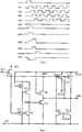
- FIG. 3 is a waveform diagram of driving signals of the GOA circuit according to an embodiment of the present disclosure.
- the GOA circuit of the present embodiment adopts four clock signals, CK1, CK2, CK3 and CK4, which are high frequency alternating current power source. Each overlap time of the clock signals is H.
- a pulse width of the clock signal is 2H, and a duty ratio is 50%.
- a high voltage level of the clock signal is 28V (adjustable).
- a low voltage level of the clock signal can be -8V (adjustable).
- STV is a trigger signal, and is a high frequency alternating current power source, and a pulse width is 2H.
- the STV signal is turned on each frame, a high voltage level is 28V, a low voltage level is -8V; the overlap of the STV and CK1 is H; VSS DC is a direct current power source, and is -6v (adjustable).
- Q(N), G(N), ST(N-2), ST(N) and P(N) are important nodes in the circuit.
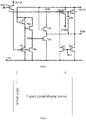
- FIG. 4 is a schematic circuit diagram of previous two stages of the GOA unit in the embodiment in FIG. 2
- FIG. 5 is a schematic circuit diagram of last two stages of the GOA unit of the GOA circuit of the present disclosure.
- the thin-film transistor T11 in the pulling-up module of the GOA unit in FIG. 4 adopts STV to control a gate and a drain of the thin-film transistor T11.
- the pull-down unit of the GOA unit in FIG. 5 adopts STV to control.
- G(N) is controlled by CK3
- G(N-2) is controlled by CK1
- G(N+2) is controlled by CK1.
- G(N) When G(N) is working: CK3 becomes a high level, G(N) outputs a high level, Q(N) will generate a higher voltage level because of capacitive coupling effect. Besides, at this time, G(N-2), ST(N-2) are at a low level, which will not affect the high level of the Q point; when G(N+2) is working: G(N+2) is a high level, at this time, T31 and T41 are turned on, Q(N) and G(N) are pulled down to a low level.
- CK3 will be at a high level periodically so that when P(N) is at a high level, T42 will be turned on periodically, and G(N) will reach a low voltage level well.
- T32 is controlled by CK(N)
- T32 will be turned on periodically so that Q(N) will maintained at a low voltage level well.
- TFTs are less in the present patent, which is beneficial to a narrow frame design. Besides, because T32 and T42 are connected in series, the resistance become larger, which decrease the risk of pulling down the high voltage level of Q(N) to a low voltage level because of current leakage of TFT so as to ensure a normal waveform of Q(N) and ensure a normal turning-on of G(N).
- the GOA circuit provided by the present disclosure can ensure to finish a displaying and driving of liquid crystals, greatly simplify the circuit design, save the cost of the circuit, and reduce the size of the GOA circuit so that the liquid crystal display device can have a design space for a narrower frame.
- FIG. 6 is a schematic diagram of a liquid crystal display device according to an embodiment of the present disclosure.
- the liquid crystal display device includes a liquid crystal panel 1 and a GOA circuit 2.
- the GOA circuit 2 is the GOA circuit in anyone of the above embodiments.
- Other structure features of the liquid crystal display device is within the understandable range for person of ordinary skilled in the art, no more repeating.
Landscapes
- Physics & Mathematics (AREA)
- Engineering & Computer Science (AREA)
- General Physics & Mathematics (AREA)
- Crystallography & Structural Chemistry (AREA)
- Chemical & Material Sciences (AREA)
- Theoretical Computer Science (AREA)
- Computer Hardware Design (AREA)
- Nonlinear Science (AREA)
- Mathematical Physics (AREA)
- Optics & Photonics (AREA)
- Control Of Indicators Other Than Cathode Ray Tubes (AREA)
- Liquid Crystal Display Device Control (AREA)
- Liquid Crystal (AREA)
Abstract
Description
- The present disclosure relates to a liquid crystal display technology field, and more particularly to a liquid crystal display device and a GOA circuit thereof.
- A GOA circuit based on a-Si is widely applied in various sizes of display devices. The GOA technology is beneficial for decreasing the cost, and a narrow frame design.
-
FIG. 1 is a schematic diagram of a GOA circuit in present technology. In one stage of the GOA circuit, 17 TFTs are adopted. However, for an amorphous silicon GOA circuit, the increase of the number of TFT will increase the size of the frame. In the trend of the development of the narrow frame, the structure of the GOA circuit in present technology cannot meet the design requirement of a narrow frame. - The embodiments of the present disclosure provides a liquid crystal display device and a GOA circuit thereof, which can solve the technology problem of not narrow enough of the display frame because of the complex structure of the GOA circuit.
- In order to solve the above problem, the embodiment of the present disclosure provides a GOA circuit comprising multiple cascaded GOA units, wherein a N-th stage GOA unit of the multiple cascaded GOA units comprises: a pull-up control module, a pull-up module, a transmission module, a pull-down module, a pull-down maintaining module and a bootstrap capacitor; wherein, the pull-up control module is connected with the transmission module and a pull-down maintaining module, one terminal of the bootstrap capacitor is connected to the transmission module and the pull-up module, the pull-down module is connected to the transmission module and a scanning line of the present stage, the pull-down maintaining module and the pull-down module are also connected with a pull-down signal line, and the pull-up module is connected with a clock signal line and the scanning line of the present stage.
- In order to solve the above technical problems, the embodiment of the present disclosure also provides a liquid crystal display device, and the liquid crystal display device includes anyone of the GOA circuits in the above embodiments.
- Comparing to the present technology, the liquid crystal display device and the GOA circuit thereof of the present disclosure can ensure to finish a displaying and driving of liquid crystals, greatly simplify the circuit design, save the cost of the circuit, and reduce the size of the GOA circuit so that the liquid crystal display device can have a design space for a narrower frame.
- In order to more clearly illustrate the technical solution of embodiments of the present disclosure, the following will illustrate the figures used for describing the embodiments. It is obvious that the following figures are only some embodiments of the present disclosure. For a skilled person in the art can also obtain other figures according to these figures without creative effort.
-
FIG. 1 is a schematic diagram of a common GOA circuit in present technology; -
FIG. 2 is a schematic circuit diagram of a N-th GOA unit according to an embodiment of the present disclosure; -
FIG. 3 is a waveform diagram of driving signals of the GOA circuit in the embodiment; -
FIG. 4 is a schematic diagram of first two stages of GOA units in the embodiment shown inFIG. 2 ; -
FIG. 5 is a schematic diagram of last two stages of GOA units in the GOA circuit of the present disclosure; -
FIG. 6 is a schematic diagram of a liquid crystal display device according to an embodiment of the present disclosure. - The following content combines with the drawings and the embodiment for describing the present disclosure in detail. It is obvious that the following embodiments are only some embodiments of the present disclosure. For a skilled person in the art, other embodiments can be obtained without creative effort thereby are still falling the scope protected by the present disclosure.
- The embodiment of the present disclosure firstly provides a GOA circuit, and the GOA circuit includes multiple cascaded GOA units. The connection and control relationship of the cascaded GOA units is in an understandable range for a skilled person in the art, no more repeating. The following will describe an N-th GOA unit in detail.
- With reference to
FIG. 2, and FIG. 2 is a schematic circuit diagram of an N-th GOA unit according to an embodiment of the present disclosure. The N-th GOA unit includes a pull-upcontrol module 100, a pull-upmodule 200, atransmission module 300, a pull-down module 400, a pull-down maintainingmodule 500 and abootstrap capacitor 600. - Specifically, the pull-up
control module 100 is connected with thetransmission module 300 and a pull-down maintainingmodule 500. One terminal of thebootstrap capacitor 600 is connected to thetransmission module 300 and the pull-upmodule 200. The pull-down module 400 is connected to thetransmission module 300 and thescanning line 700 of the present stage. The pull-down maintainingmodule 500 and the pull-down module 400 are also connected with a pull-down signal line 800. The pull-upmodule 200 is connected with aclock signal line 900 and thescanning line 700 of the present stage. - Wherein, the pull-up
control module 100 includes a first thin-film transistor T11, a gate of the first thin-film transistor T11 is used for receiving a trigger signal ST(N-2) of an (N-2)-th stage GOA unit, a source of the first thin-film transistor T11 is used for connecting a scanning line signal G(N-2) of the (N-2)-th stage GOA unit, and a drain of the first thin-film transistor T11 is connected with thetransmission module 300 and the pull-down maintainingmodule 500. - The
transmission module 300 includes a second thin-film transistor T22. A gate of the second thin-film transistor T22 is connected with the drain of the first thin-film transistor T11, a source of the second thin-film transistor T22 is connected with theclock signal line 900, and a drain of the second thin-film transistor T22 is used for outputting a trigger signal ST(N) of the present stage GOA unit. - The pull-up
module 200 includes a third thin-film transistor T21, a gate of the third thin-film transistor T21 is connected with the drain of the first thin-film transistor T11, a source of the third thin-film transistor T21 is connected with theclock signal 900, and a drain of the third thin-film transistor T21 is connected with thescanning line 700 of the present stage. - One terminal of the
bootstrap capacitor 600 is connected with the gate of the second thin-film transistor T22 and the gate of the third thin-film transistor T21, and the other terminal of thebootstrap capacitor 600 is connected with thescanning line 700 of the present stage. - The pull-
down module 400 includes a fourth thin-film transistor T41 and a fifth thin-film transistor T31. A gate of the fourth thin-film transistor T41 is used for receiving a scanning line signal G(N+2) of an (N+2)-th stage GOA unit, a source of the fourth thin-film transistor T41 is connected with the drain of the first thin-film transistor T11, a drain of the fourth thin-film transistor T41 is connected with the pull-down signal line 800. A gate of the fifth thin-film transistor T31 is used for receiving the scanning line signal G(N+2) of the (N+2)-th stage GOA unit, a source of the fifth thin-film transistor T31 is connected with thescanning line 700 of the present stage, and a drain of the fifth thin-film transistor T31 is connected with the pull-down signal line 800. - The pull-down maintaining
module 500 includes a sixth thin-film transistor T51, a seventh thin-film transistor T53, an eighth thin-film transistor T32, a ninth thin-film transistor T42, a tenth thin-film transistor T52 and an eleventh thin-film transistor T54. A gate of the sixth thin-film transistor T51 is connected with theclock signal line 900, a source of the sixth thin-film transistor T51 is connected with a source of the seventh thin-film transistor T53, a drain of the sixth thin-film transistor T51 is connected with a gate of the seventh thin-film transistor T53, and a source of the tenth thin-film transistor T52. A drain of the seventh thin-film transistor T53 is connected with a gate of the ninth thin-film transistor T42 and a source of the eleventh thin-film transistor T54. A gate of the eighth thin-film transistor T32 is connected with theclock signal line 900, a source of the eighth thin-film transistor T32 is connected with the drain of the first thin-film transistor T11, and a drain of the eighth thin-film transistor T32 is connected with thescanning line 700 of the present stage and a source of the ninth thin-film transistor T42. A drain of the ninth thin-film transistor T42 is connected with the pull-down signal line 800. A gate of the tenth thin-film transistor T52 is connected with a drain of the first thin-film transistor T11. A drain of the tenth thin-film transistor T52 is connected with the pull-down signal line 800. A gate of the eleventh thin-film transistor T54 is connected with a drain of the first thin-film transistor T11, a drain of the eleventh thin-film transistor T54 is connected with the pull-down signal line 800. - Wherein, the source of the eighth thin-film transistor T32 is connected with the drain of the first thin-film transistor T11 through a first node Q(N); the drain of the seventh thin-film transistor T53, the gate of the ninth thin-film transistor T42 and the source of the eleventh thin-film transistor T54 are connected with each other through a second node P(N).
- With reference to
FIG. 3, and FIG. 3 is a waveform diagram of driving signals of the GOA circuit according to an embodiment of the present disclosure. The GOA circuit of the present embodiment adopts four clock signals, CK1, CK2, CK3 and CK4, which are high frequency alternating current power source. Each overlap time of the clock signals is H. A pulse width of the clock signal is 2H, and a duty ratio is 50%. A high voltage level of the clock signal is 28V (adjustable). A low voltage level of the clock signal can be -8V (adjustable). STV is a trigger signal, and is a high frequency alternating current power source, and a pulse width is 2H. The STV signal is turned on each frame, a high voltage level is 28V, a low voltage level is -8V; the overlap of the STV and CK1 is H; VSS DC is a direct current power source, and is -6v (adjustable). Q(N), G(N), ST(N-2), ST(N) and P(N) are important nodes in the circuit. - The following adopts an N-th stage GOA circuit as an example for illustrating conceptually. Furthermore, with reference to
FIG. 4 andFIG. 5 ,FIG. 4 is a schematic circuit diagram of previous two stages of the GOA unit in the embodiment inFIG. 2 , andFIG. 5 is a schematic circuit diagram of last two stages of the GOA unit of the GOA circuit of the present disclosure. The thin-film transistor T11 in the pulling-up module of the GOA unit inFIG. 4 adopts STV to control a gate and a drain of the thin-film transistor T11. The pull-down unit of the GOA unit inFIG. 5 adopts STV to control. - According to the waveforms shown in
FIG. 3 , G(N) is controlled by CK3, G(N-2) is controlled by CK1, G(N+2) is controlled by CK1. - When G(N-2) is working: when G(N-2), ST(N-2) are at a high level, the high level of the G(N-2) is inputted to Q(N), T21 is turned on. At this time, CK(N)=CK3, which is a low level, and G(N) outputs a low level.
- When G(N) is working: CK3 becomes a high level, G(N) outputs a high level, Q(N) will generate a higher voltage level because of capacitive coupling effect. Besides, at this time, G(N-2), ST(N-2) are at a low level, which will not affect the high level of the Q point; when G(N+2) is working: G(N+2) is a high level, at this time, T31 and T41 are turned on, Q(N) and G(N) are pulled down to a low level.
- Subsequently, CK3 will be at a high level periodically so that when P(N) is at a high level, T42 will be turned on periodically, and G(N) will reach a low voltage level well. At the same time, because T32 is controlled by CK(N), T32 will be turned on periodically so that Q(N) will maintained at a low voltage level well.
- The number of TFTs is less in the present patent, which is beneficial to a narrow frame design. Besides, because T32 and T42 are connected in series, the resistance become larger, which decrease the risk of pulling down the high voltage level of Q(N) to a low voltage level because of current leakage of TFT so as to ensure a normal waveform of Q(N) and ensure a normal turning-on of G(N).
- The GOA circuit provided by the present disclosure can ensure to finish a displaying and driving of liquid crystals, greatly simplify the circuit design, save the cost of the circuit, and reduce the size of the GOA circuit so that the liquid crystal display device can have a design space for a narrower frame.
- Besides, the embodiment of the present disclosure also provides a liquid crystal display device. With reference to
FIG. 6, and FIG. 6 is a schematic diagram of a liquid crystal display device according to an embodiment of the present disclosure. The liquid crystal display device includes aliquid crystal panel 1 and aGOA circuit 2. Wherein, theGOA circuit 2 is the GOA circuit in anyone of the above embodiments. Other structure features of the liquid crystal display device is within the understandable range for person of ordinary skilled in the art, no more repeating. - The above embodiments of the present disclosure are not used to limit the claims of the present disclosure. Any use of the content in the specification or in the drawings of the present disclosure which produces equivalent structures or equivalent processes, or directly or indirectly used in other related technical fields is still covered by the claims in the present disclosure.
Claims (19)
- A GOA circuit comprising multiple cascaded GOA units, wherein a N-th stage GOA unit of the multiple cascaded GOA units comprises: a pull-up control module, a pull-up module, a transmission module, a pull-down module, a pull-down maintaining module and a bootstrap capacitor; wherein, the pull-up control module is connected with the transmission module and the pull-down maintaining module, one terminal of the bootstrap capacitor is connected to the transmission module and the pull-up module, the pull-down module is connected to the transmission module and a scanning line of the present stage, the pull-down maintaining module and the pull-down module are connected with a pull-down signal line, and the pull-up module is connected with a clock signal line and the scanning line of the present stage; the pull-up control module includes a first thin-film transistor T11, a gate of the first thin-film transistor T11 is used for receiving a trigger signal of an (N-2)-th stage GOA unit, a source of the first thin-film transistor T11 is used for connecting a scanning line signal of the (N-2)-th stage GOA unit, and a drain of the first thin-film transistor T11 is connected with the transmission module and the pull-down maintaining module; the pull-down maintaining module 500 includes a sixth thin-film transistor T51, a seventh thin-film transistor T53, an eighth thin-film transistor T32, a ninth thin-film transistor T42, a tenth thin-film transistor T52 and an eleventh thin-film transistor T54; a gate of the sixth thin-film transistor T51 is connected with the clock signal line, a source of the sixth thin-film transistor T51 is connected with a source of the seventh thin-film transistor T53, a drain of the sixth thin-film transistor T51 is connected with a gate of the seventh thin-film transistor T53 and a source of the tenth thin-film transistor T52; a drain of the seventh thin-film transistor T53 is connected with a gate of the ninth thin-film transistor T42 and a source of the eleventh thin-film transistor T54; a gate of the eighth thin-film transistor T32 is connected with the clock signal line, a source of the eighth thin-film transistor T32 is connected with the drain of the first thin-film transistor T11, and a drain of the eighth thin-film transistor T32 is connected with the scanning line of the present stage and a source of the ninth thin-film transistor T42; a drain of the ninth thin-film transistor T42 is connected with the pull-down signal line; a gate of the tenth thin-film transistor T52 is connected with a drain of the first thin-film transistor T11; a drain of the tenth thin-film transistor T52 is connected with the pull-down signal line; a gate of the eleventh thin-film transistor T54 is connected with a drain of the first thin-film transistor T11, a drain of the eleventh thin-film transistor T54 is connected with the pull-down signal line.
- A GOA circuit comprising multiple cascaded GOA units, wherein a N-th stage GOA unit of the multiple cascaded GOA units comprises: a pull-up control module, a pull-up module, a transmission module, a pull-down module, a pull-down maintaining module and a bootstrap capacitor; wherein, the pull-up control module is connected with the transmission module and a pull-down maintaining module, one terminal of the bootstrap capacitor is connected to the transmission module and the pull-up module, the pull-down module is connected to the transmission module and a scanning line of the present stage, the pull-down maintaining module and the pull-down module are also connected with a pull-down signal line, and the pull-up module is connected with a clock signal line and the scanning line of the present stage.
- The GOA circuit according to claim 2, wherein, the pull-up control module includes a first thin-film transistor T11, a gate of the first thin-film transistor T11 is used for receiving a trigger signal of an (N-2)-th stage GOA unit, a source of the first thin-film transistor T11 is used for connecting a scanning line signal of the (N-2)-th stage GOA unit, and a drain of the first thin-film transistor T11 is connected with the transmission module and the pull-down maintaining module.
- The GOA circuit according to claim 3, wherein, the transmission module includes a second thin-film transistor T22, a gate of the second thin-film transistor T22 is connected with the drain of the first thin-film transistor T11, a source of the second thin-film transistor T22 is connected with the clock signal line, and a drain of the second thin-film transistor T22 is used for outputting a trigger signal of the present stage GOA unit.
- The GOA circuit according to claim 4, wherein, the pull-up module includes a third thin-film transistor T21, a gate of the third thin-film transistor T21 is connected with the drain of the first thin-film transistor T11, a source of the third thin-film transistor T21 is connected with the clock signal, and a drain of the third thin-film transistor T21 is connected with the scanning line of the present stage.
- The GOA circuit according to claim 5, wherein, one terminal of the bootstrap capacitor is connected with the gate of the second thin-film transistor T22 and the gate of the third thin-film transistor T21, and the other terminal of the bootstrap capacitor is connected with the scanning line of the present stage.
- The GOA circuit according to claim 6, wherein, the pull-down module includes a fourth thin-film transistor T41 and a fifth thin-film transistor T31, a gate of the fourth thin-film transistor T41 is used for receiving a scanning line signal of an (N+2)-th stage GOA unit, a source of the fourth thin-film transistor T41 is connected with the drain of the first thin-film transistor T11, a drain of the fourth thin-film transistor T41 is connected with the pull-down signal line; a gate of the fifth thin-film transistor T31 is used for receiving the scanning line signal of the (N+2)-th stage GOA unit, a source of the fifth thin-film transistor T31 is connected with the scanning line of the present stage, and a drain of the fifth thin-film transistor T31 is connected with the pull-down signal line.
- The GOA circuit according to claim 2, wherein, the pull-down maintaining module 500 includes a sixth thin-film transistor T51, a seventh thin-film transistor T53, an eighth thin-film transistor T32, a ninth thin-film transistor T42, a tenth thin-film transistor T52 and an eleventh thin-film transistor T54; a gate of the sixth thin-film transistor T51 is connected with the clock signal line, a source of the sixth thin-film transistor T51 is connected with a source of the seventh thin-film transistor T53, a drain of the sixth thin-film transistor T51 is connected with a gate of the seventh thin-film transistor T53 and a source of the tenth thin-film transistor T52; a drain of the seventh thin-film transistor T53 is connected with a gate of the ninth thin-film transistor T42 and a source of the eleventh thin-film transistor T54; a gate of the eighth thin-film transistor T32 is connected with the clock signal line, a source of the eighth thin-film transistor T32 is connected with the drain of the first thin-film transistor T11, and a drain of the eighth thin-film transistor T32 is connected with the scanning line of the present stage and a source of the ninth thin-film transistor T42; a drain of the ninth thin-film transistor T42 is connected with the pull-down signal line; a gate of the tenth thin-film transistor T52 is connected with a drain of the first thin-film transistor T11; a drain of the tenth thin-film transistor T52 is connected with the pull-down signal line; a gate of the eleventh thin-film transistor T54 is connected with a drain of the first thin-film transistor T11, a drain of the eleventh thin-film transistor T54 is connected with the pull-down signal line.
- The GOA circuit according to claim 8, wherein, the source of the eighth thin-film transistor T32 is connected with the drain of the first thin-film transistor T11 through a first node Q(N).
- The GOA circuit according to claim 8, wherein, the drain of the seventh thin-film transistor T53, the gate of the ninth thin-film transistor T42, and the source of the eleventh thin-film transistor T54 are connected with each other through a second node P(N).
- A liquid crystal display device, wherein the liquid crystal display device includes a GOA circuit, and the GOA circuit comprises multiple cascaded GOA units, wherein a N-th stage GOA unit of the multiple cascaded GOA units comprises: a pull-up control module, a pull-up module, a transmission module, a pull-down module, a pull-down maintaining module and a bootstrap capacitor; wherein, the pull-up control module is connected with the transmission module and a pull-down maintaining module, one terminal of the bootstrap capacitor is connected to the transmission module and the pull-up module, the pull-down module is connected to the transmission module and a scanning line of the present stage, the pull-down maintaining module and the pull-down module are also connected with a pull-down signal line, and the pull-up module is connected with a clock signal line and the scanning line of the present stage.
- The liquid crystal display device according to claim 11, the pull-up control module includes a first thin-film transistor T11, a gate of the first thin-film transistor T11 is used for receiving a trigger signal of an (N-2)-th stage GOA unit, a source of the first thin-film transistor T11 is used for connecting a scanning line signal of the (N-2)-th stage GOA unit, and a drain of the first thin-film transistor T11 is connected with the transmission module and the pull-down maintaining module.
- The liquid crystal display device according to claim 12, wherein, the transmission module includes a second thin-film transistor T22, a gate of the second thin-film transistor T22 is connected with the drain of the first thin-film transistor T11, a source of the second thin-film transistor T22 is connected with the clock signal line, and a drain of the second thin-film transistor T22 is used for outputting a trigger signal of the present stage GOA unit.
- The liquid crystal display device according to claim 13, wherein, the pull-up module includes a third thin-film transistor T21, a gate of the third thin-film transistor T21 is connected with the drain of the first thin-film transistor T11, a source of the third thin-film transistor T21 is connected with the clock signal, and a drain of the third thin-film transistor T21 is connected with the scanning line of the present stage.
- The liquid crystal display device according to claim 14, wherein, one terminal of the bootstrap capacitor is connected with the gate of the second thin-film transistor T22 and the gate of the third thin-film transistor T21, and the other terminal of the bootstrap capacitor is connected with the scanning line of the present stage.
- The liquid crystal display device according to claim 15, wherein, the pull-down module includes a fourth thin-film transistor T41 and a fifth thin-film transistor T31, a gate of the fourth thin-film transistor T41 is used for receiving a scanning line signal of an (N+2)-th stage GOA unit, a source of the fourth thin-film transistor T41 is connected with the drain of the first thin-film transistor T11, a drain of the fourth thin-film transistor T41 is connected with the pull-down signal line; a gate of the fifth thin-film transistor T31 is used for receiving the scanning line signal of the (N+2)-th stage GOA unit, a source of the fifth thin-film transistor T31 is connected with the scanning line of the present stage, and a drain of the fifth thin-film transistor T31 is connected with the pull-down signal line.
- The liquid crystal display device according to claim 11, wherein, the pull-down maintaining module 500 includes a sixth thin-film transistor T51, a seventh thin-film transistor T53, an eighth thin-film transistor T32, a ninth thin-film transistor T42, a tenth thin-film transistor T52 and an eleventh thin-film transistor T54; a gate of the sixth thin-film transistor T51 is connected with the clock signal line, a source of the sixth thin-film transistor T51 is connected with a source of the seventh thin-film transistor T53, a drain of the sixth thin-film transistor T51 is connected with a gate of the seventh thin-film transistor T53 and a source of the tenth thin-film transistor T52; a drain of the seventh thin-film transistor T53 is connected with a gate of the ninth thin-film transistor T42 and a source of the eleventh thin-film transistor T54; a gate of the eighth thin-film transistor T32 is connected with the clock signal line, a source of the eighth thin-film transistor T32 is connected with the drain of the first thin-film transistor T11, and a drain of the eighth thin-film transistor T32 is connected with the scanning line of the present stage and a source of the ninth thin-film transistor T42; a drain of the ninth thin-film transistor T42 is connected with the pull-down signal line; a gate of the tenth thin-film transistor T52 is connected with a drain of the first thin-film transistor T11; a drain of the tenth thin-film transistor T52 is connected with the pull-down signal line; a gate of the eleventh thin-film transistor T54 is connected with a drain of the first thin-film transistor T11, a drain of the eleventh thin-film transistor T54 is connected with the pull-down signal line.
- The liquid crystal display device according to claim 17, wherein, the source of the eighth thin-film transistor T32 is connected with the drain of the first thin-film transistor T11 through a first node Q(N).
- The liquid crystal display device according to claim 17, wherein, the drain of the seventh thin-film transistor T53, the gate of the ninth thin-film transistor T42 and the source of the eleventh thin-film transistor T54 are connected with each other through a second node P(N).
Applications Claiming Priority (2)
| Application Number | Priority Date | Filing Date | Title |
|---|---|---|---|
| CN201710229984.4A CN107086028B (en) | 2017-04-10 | 2017-04-10 | Liquid crystal display device and its GOA circuit |
| PCT/CN2017/081976 WO2018188119A1 (en) | 2017-04-10 | 2017-04-26 | Liquid crystal display device and goa circuit thereof |
Publications (2)
| Publication Number | Publication Date |
|---|---|
| EP3611721A1 true EP3611721A1 (en) | 2020-02-19 |
| EP3611721A4 EP3611721A4 (en) | 2020-10-28 |
Family
ID=59611302
Family Applications (1)
| Application Number | Title | Priority Date | Filing Date |
|---|---|---|---|
| EP17905458.0A Withdrawn EP3611721A4 (en) | 2017-04-10 | 2017-04-26 | LIQUID CRYSTAL DISPLAY DEVICE AND GOA CIRCUIT FOR IT |
Country Status (6)
| Country | Link |
|---|---|
| US (1) | US10269318B2 (en) |
| EP (1) | EP3611721A4 (en) |
| JP (1) | JP2020509425A (en) |
| KR (1) | KR20190131593A (en) |
| CN (1) | CN107086028B (en) |
| WO (1) | WO2018188119A1 (en) |
Families Citing this family (8)
| Publication number | Priority date | Publication date | Assignee | Title |
|---|---|---|---|---|
| CN107154245B (en) * | 2017-07-17 | 2019-06-25 | 深圳市华星光电技术有限公司 | A kind of gate driving circuit and its driving method |
| CN108172181A (en) * | 2017-12-21 | 2018-06-15 | 深圳市华星光电技术有限公司 | A kind of GOA circuits and liquid crystal display panel |
| CN109036307B (en) * | 2018-07-27 | 2019-06-21 | 深圳市华星光电技术有限公司 | Liquid crystal panel including GOA circuit and driving method thereof |
| CN113168880A (en) * | 2018-12-28 | 2021-07-23 | 深圳市柔宇科技股份有限公司 | GOA unit and its GOA circuit, display device |
| CN111161689B (en) * | 2020-02-12 | 2021-07-06 | 武汉华星光电技术有限公司 | GOA circuit and display panel thereof |
| CN113362752A (en) | 2021-06-01 | 2021-09-07 | 深圳市华星光电半导体显示技术有限公司 | GOA circuit and display panel |
| CN115862511B (en) * | 2022-11-30 | 2024-04-12 | Tcl华星光电技术有限公司 | Gate drive circuit and display panel |
| CN117912420B (en) * | 2024-02-29 | 2025-10-17 | 长沙惠科光电有限公司 | Scanning driving circuit, array substrate, display panel and display device |
Family Cites Families (10)
| Publication number | Priority date | Publication date | Assignee | Title |
|---|---|---|---|---|
| JP5079301B2 (en) | 2006-10-26 | 2012-11-21 | 三菱電機株式会社 | Shift register circuit and image display apparatus including the same |
| CN103956146B (en) * | 2014-04-17 | 2017-04-12 | 深圳市华星光电技术有限公司 | Liquid crystal panel drive circuit, liquid crystal display device and drive method |
| CN104008739B (en) * | 2014-05-20 | 2017-04-12 | 深圳市华星光电技术有限公司 | Scan drive circuit and liquid crystal display |
| CN104167191B (en) * | 2014-07-04 | 2016-08-17 | 深圳市华星光电技术有限公司 | Complementary type GOA circuit for flat pannel display |
| CN104064158B (en) * | 2014-07-17 | 2016-05-04 | 深圳市华星光电技术有限公司 | There is the gate driver circuit of self-compensating function |
| CN104064160B (en) | 2014-07-17 | 2016-06-15 | 深圳市华星光电技术有限公司 | There is the gate driver circuit of self-compensating function |
| CN105632441B (en) * | 2016-02-26 | 2018-03-27 | 深圳市华星光电技术有限公司 | Gate driving circuit |
| CN106205528B (en) * | 2016-07-19 | 2019-04-16 | 深圳市华星光电技术有限公司 | A GOA circuit and liquid crystal display panel |
| CN106128397B (en) * | 2016-08-31 | 2019-03-15 | 深圳市华星光电技术有限公司 | A GOA drive unit and drive circuit |
| CN106328084A (en) * | 2016-10-18 | 2017-01-11 | 深圳市华星光电技术有限公司 | GOA drive circuit and liquid crystal display device |
-
2017
- 2017-04-10 CN CN201710229984.4A patent/CN107086028B/en active Active
- 2017-04-26 US US15/545,652 patent/US10269318B2/en active Active
- 2017-04-26 EP EP17905458.0A patent/EP3611721A4/en not_active Withdrawn
- 2017-04-26 KR KR1020197033216A patent/KR20190131593A/en not_active Ceased
- 2017-04-26 JP JP2019547619A patent/JP2020509425A/en active Pending
- 2017-04-26 WO PCT/CN2017/081976 patent/WO2018188119A1/en not_active Ceased
Also Published As
| Publication number | Publication date |
|---|---|
| JP2020509425A (en) | 2020-03-26 |
| WO2018188119A1 (en) | 2018-10-18 |
| CN107086028B (en) | 2018-11-20 |
| CN107086028A (en) | 2017-08-22 |
| US20180293951A1 (en) | 2018-10-11 |
| US10269318B2 (en) | 2019-04-23 |
| KR20190131593A (en) | 2019-11-26 |
| EP3611721A4 (en) | 2020-10-28 |
Similar Documents
| Publication | Publication Date | Title |
|---|---|---|
| US10269318B2 (en) | Liquid crystal display device and GOA circuit of the same | |
| CN111223433B (en) | GOA circuit and display device | |
| KR102108880B1 (en) | Gate driving circuit and a display apparatus having the gate driving circuit | |
| CN107689221B (en) | GOA circuit | |
| USRE49782E1 (en) | Shift register and driving method thereof gate driving circuit and display apparatus | |
| CN107909971B (en) | GOA circuit | |
| US8018451B2 (en) | Liquid crystal display | |
| CN111402829B (en) | GOA circuit and display panel | |
| CN107799083B (en) | GOA circuit | |
| US11640808B2 (en) | Array substrate row drive circuit unit, drive circuit and liquid crystal display panel thereof | |
| US9495929B2 (en) | Shift register, driver circuit and display device | |
| CN107808650B (en) | GOA circuit | |
| CN107492362B (en) | Grid driving circuit and liquid crystal display | |
| US20190073978A1 (en) | Goa circuit for preventing clock signals from missing | |
| US10580375B2 (en) | Gate drive circuit | |
| US10796653B2 (en) | GOA circuit | |
| US12431105B2 (en) | Display device improving response speed of a gate clock signal or eliminating delay in the gate clock signal | |
| CN106297715B (en) | A kind of the GOA circuit and liquid crystal display of the driving of three ranks | |
| GB2527715A (en) | GOA drive circuit and drive method | |
| US20180336857A1 (en) | Goa circuit and liquid crystal display device | |
| WO2019200820A1 (en) | Liquid crystal display apparatus and driving method therefor | |
| CN106409243A (en) | GOA driving circuit | |
| WO2021184544A1 (en) | Goa circuit and display panel | |
| US11837188B2 (en) | Goa circuit and display panel for reducing threshold voltage shift of transistor by pulling down signal during blank time of scan signal | |
| CN101763900A (en) | Shift register circuit |
Legal Events
| Date | Code | Title | Description |
|---|---|---|---|
| STAA | Information on the status of an ep patent application or granted ep patent |
Free format text: STATUS: THE INTERNATIONAL PUBLICATION HAS BEEN MADE |
|
| PUAI | Public reference made under article 153(3) epc to a published international application that has entered the european phase |
Free format text: ORIGINAL CODE: 0009012 |
|
| STAA | Information on the status of an ep patent application or granted ep patent |
Free format text: STATUS: REQUEST FOR EXAMINATION WAS MADE |
|
| 17P | Request for examination filed |
Effective date: 20191106 |
|
| AK | Designated contracting states |
Kind code of ref document: A1 Designated state(s): AL AT BE BG CH CY CZ DE DK EE ES FI FR GB GR HR HU IE IS IT LI LT LU LV MC MK MT NL NO PL PT RO RS SE SI SK SM TR |
|
| AX | Request for extension of the european patent |
Extension state: BA ME |
|
| DAV | Request for validation of the european patent (deleted) | ||
| DAX | Request for extension of the european patent (deleted) | ||
| A4 | Supplementary search report drawn up and despatched |
Effective date: 20200928 |
|
| RIC1 | Information provided on ipc code assigned before grant |
Ipc: G09G 3/20 20060101ALI20200922BHEP Ipc: G09G 3/36 20060101AFI20200922BHEP Ipc: G02F 1/13 20060101ALI20200922BHEP Ipc: G11C 19/28 20060101ALI20200922BHEP |
|
| STAA | Information on the status of an ep patent application or granted ep patent |
Free format text: STATUS: THE APPLICATION IS DEEMED TO BE WITHDRAWN |
|
| 18D | Application deemed to be withdrawn |
Effective date: 20210427 |