EP3611660A1 - Method of manufacturing an array of pixels from a thermal pattern sensor and associated sensor - Google Patents
Method of manufacturing an array of pixels from a thermal pattern sensor and associated sensor Download PDFInfo
- Publication number
- EP3611660A1 EP3611660A1 EP19306017.5A EP19306017A EP3611660A1 EP 3611660 A1 EP3611660 A1 EP 3611660A1 EP 19306017 A EP19306017 A EP 19306017A EP 3611660 A1 EP3611660 A1 EP 3611660A1
- Authority
- EP
- European Patent Office
- Prior art keywords
- layer
- formation
- tracks
- manufacturing
- electrically conductive
- Prior art date
- Legal status (The legal status is an assumption and is not a legal conclusion. Google has not performed a legal analysis and makes no representation as to the accuracy of the status listed.)
- Granted
Links
- 238000004519 manufacturing process Methods 0.000 title claims abstract description 27
- 239000010410 layer Substances 0.000 claims abstract description 157
- 238000000151 deposition Methods 0.000 claims abstract description 42
- 239000011159 matrix material Substances 0.000 claims abstract description 36
- 230000008021 deposition Effects 0.000 claims abstract description 32
- 239000000463 material Substances 0.000 claims abstract description 31
- 238000000034 method Methods 0.000 claims abstract description 24
- 238000010438 heat treatment Methods 0.000 claims abstract description 21
- 239000007788 liquid Substances 0.000 claims abstract description 13
- 239000004020 conductor Substances 0.000 claims abstract description 11
- 239000000758 substrate Substances 0.000 claims abstract description 10
- 239000003989 dielectric material Substances 0.000 claims abstract description 6
- 239000011241 protective layer Substances 0.000 claims abstract description 4
- 230000015572 biosynthetic process Effects 0.000 claims description 47
- 229910052751 metal Inorganic materials 0.000 claims description 12
- 239000002184 metal Substances 0.000 claims description 12
- WYTGDNHDOZPMIW-RCBQFDQVSA-N alstonine Natural products C1=CC2=C3C=CC=CC3=NC2=C2N1C[C@H]1[C@H](C)OC=C(C(=O)OC)[C@H]1C2 WYTGDNHDOZPMIW-RCBQFDQVSA-N 0.000 claims description 4
- 238000003491 array Methods 0.000 claims description 2
- 238000007639 printing Methods 0.000 description 11
- 238000005520 cutting process Methods 0.000 description 10
- 230000010287 polarization Effects 0.000 description 5
- 229910052709 silver Inorganic materials 0.000 description 5
- BQCADISMDOOEFD-UHFFFAOYSA-N Silver Chemical compound [Ag] BQCADISMDOOEFD-UHFFFAOYSA-N 0.000 description 4
- 230000000295 complement effect Effects 0.000 description 4
- 238000001514 detection method Methods 0.000 description 4
- 238000010020 roller printing Methods 0.000 description 4
- 239000004332 silver Substances 0.000 description 4
- 239000002033 PVDF binder Substances 0.000 description 3
- 229910052782 aluminium Inorganic materials 0.000 description 3
- 229910052802 copper Inorganic materials 0.000 description 3
- 239000010949 copper Substances 0.000 description 3
- 229910052737 gold Inorganic materials 0.000 description 3
- 239000010931 gold Substances 0.000 description 3
- 239000007769 metal material Substances 0.000 description 3
- 229920000139 polyethylene terephthalate Polymers 0.000 description 3
- 239000005020 polyethylene terephthalate Substances 0.000 description 3
- 229920002981 polyvinylidene fluoride Polymers 0.000 description 3
- RYGMFSIKBFXOCR-UHFFFAOYSA-N Copper Chemical compound [Cu] RYGMFSIKBFXOCR-UHFFFAOYSA-N 0.000 description 2
- XAGFODPZIPBFFR-UHFFFAOYSA-N aluminium Chemical compound [Al] XAGFODPZIPBFFR-UHFFFAOYSA-N 0.000 description 2
- 238000005137 deposition process Methods 0.000 description 2
- 239000011521 glass Substances 0.000 description 2
- PCHJSUWPFVWCPO-UHFFFAOYSA-N gold Chemical compound [Au] PCHJSUWPFVWCPO-UHFFFAOYSA-N 0.000 description 2
- 238000007645 offset printing Methods 0.000 description 2
- 238000000206 photolithography Methods 0.000 description 2
- 230000001681 protective effect Effects 0.000 description 2
- MIZLGWKEZAPEFJ-UHFFFAOYSA-N 1,1,2-trifluoroethene Chemical group FC=C(F)F MIZLGWKEZAPEFJ-UHFFFAOYSA-N 0.000 description 1
- 229920000144 PEDOT:PSS Polymers 0.000 description 1
- 239000004642 Polyimide Substances 0.000 description 1
- XUIMIQQOPSSXEZ-UHFFFAOYSA-N Silicon Chemical compound [Si] XUIMIQQOPSSXEZ-UHFFFAOYSA-N 0.000 description 1
- 239000011248 coating agent Substances 0.000 description 1
- 238000000576 coating method Methods 0.000 description 1
- 239000000470 constituent Substances 0.000 description 1
- 230000005684 electric field Effects 0.000 description 1
- 230000002349 favourable effect Effects 0.000 description 1
- 238000007646 gravure printing Methods 0.000 description 1
- 230000010354 integration Effects 0.000 description 1
- 238000001459 lithography Methods 0.000 description 1
- 238000005259 measurement Methods 0.000 description 1
- 125000005487 naphthalate group Chemical group 0.000 description 1
- -1 polyethylene terephthalate Polymers 0.000 description 1
- 229920001721 polyimide Polymers 0.000 description 1
- 229920002620 polyvinyl fluoride Polymers 0.000 description 1
- 239000010970 precious metal Substances 0.000 description 1
- QEVHRUUCFGRFIF-MDEJGZGSSA-N reserpine Chemical compound O([C@H]1[C@@H]([C@H]([C@H]2C[C@@H]3C4=C(C5=CC=C(OC)C=C5N4)CCN3C[C@H]2C1)C(=O)OC)OC)C(=O)C1=CC(OC)=C(OC)C(OC)=C1 QEVHRUUCFGRFIF-MDEJGZGSSA-N 0.000 description 1
- 239000004065 semiconductor Substances 0.000 description 1
- 229910052710 silicon Inorganic materials 0.000 description 1
- 239000010703 silicon Substances 0.000 description 1
- 238000005987 sulfurization reaction Methods 0.000 description 1
- 238000001771 vacuum deposition Methods 0.000 description 1
Images


Classifications
-
- G—PHYSICS
- G01—MEASURING; TESTING
- G01J—MEASUREMENT OF INTENSITY, VELOCITY, SPECTRAL CONTENT, POLARISATION, PHASE OR PULSE CHARACTERISTICS OF INFRARED, VISIBLE OR ULTRAVIOLET LIGHT; COLORIMETRY; RADIATION PYROMETRY
- G01J5/00—Radiation pyrometry, e.g. infrared or optical thermometry
- G01J5/10—Radiation pyrometry, e.g. infrared or optical thermometry using electric radiation detectors
- G01J5/34—Radiation pyrometry, e.g. infrared or optical thermometry using electric radiation detectors using capacitors, e.g. pyroelectric capacitors
-
- A—HUMAN NECESSITIES
- A61—MEDICAL OR VETERINARY SCIENCE; HYGIENE
- A61B—DIAGNOSIS; SURGERY; IDENTIFICATION
- A61B5/00—Measuring for diagnostic purposes; Identification of persons
- A61B5/117—Identification of persons
- A61B5/1171—Identification of persons based on the shapes or appearances of their bodies or parts thereof
- A61B5/1172—Identification of persons based on the shapes or appearances of their bodies or parts thereof using fingerprinting
-
- G—PHYSICS
- G01—MEASURING; TESTING
- G01K—MEASURING TEMPERATURE; MEASURING QUANTITY OF HEAT; THERMALLY-SENSITIVE ELEMENTS NOT OTHERWISE PROVIDED FOR
- G01K7/00—Measuring temperature based on the use of electric or magnetic elements directly sensitive to heat ; Power supply therefor, e.g. using thermoelectric elements
- G01K7/003—Measuring temperature based on the use of electric or magnetic elements directly sensitive to heat ; Power supply therefor, e.g. using thermoelectric elements using pyroelectric elements
-
- G—PHYSICS
- G06—COMPUTING; CALCULATING OR COUNTING
- G06V—IMAGE OR VIDEO RECOGNITION OR UNDERSTANDING
- G06V40/00—Recognition of biometric, human-related or animal-related patterns in image or video data
- G06V40/10—Human or animal bodies, e.g. vehicle occupants or pedestrians; Body parts, e.g. hands
- G06V40/12—Fingerprints or palmprints
- G06V40/13—Sensors therefor
- G06V40/1306—Sensors therefor non-optical, e.g. ultrasonic or capacitive sensing
-
- G—PHYSICS
- G06—COMPUTING; CALCULATING OR COUNTING
- G06V—IMAGE OR VIDEO RECOGNITION OR UNDERSTANDING
- G06V40/00—Recognition of biometric, human-related or animal-related patterns in image or video data
- G06V40/10—Human or animal bodies, e.g. vehicle occupants or pedestrians; Body parts, e.g. hands
- G06V40/12—Fingerprints or palmprints
- G06V40/13—Sensors therefor
- G06V40/1329—Protecting the fingerprint sensor against damage caused by the finger
-
- G—PHYSICS
- G06—COMPUTING; CALCULATING OR COUNTING
- G06V—IMAGE OR VIDEO RECOGNITION OR UNDERSTANDING
- G06V40/00—Recognition of biometric, human-related or animal-related patterns in image or video data
- G06V40/10—Human or animal bodies, e.g. vehicle occupants or pedestrians; Body parts, e.g. hands
- G06V40/12—Fingerprints or palmprints
- G06V40/1335—Combining adjacent partial images (e.g. slices) to create a composite input or reference pattern; Tracking a sweeping finger movement
-
- H—ELECTRICITY
- H10—SEMICONDUCTOR DEVICES; ELECTRIC SOLID-STATE DEVICES NOT OTHERWISE PROVIDED FOR
- H10N—ELECTRIC SOLID-STATE DEVICES NOT OTHERWISE PROVIDED FOR
- H10N15/00—Thermoelectric devices without a junction of dissimilar materials; Thermomagnetic devices, e.g. using the Nernst-Ettingshausen effect
- H10N15/10—Thermoelectric devices using thermal change of the dielectric constant, e.g. working above and below the Curie point
Definitions
- the invention relates to a method for manufacturing a thermal pattern sensor, for example a so-called “active” fingerprint sensor, performing active or passive thermal detection and preferably comprising an active or passive matrix of pixels.
- the invention relates more particularly to the manufacture of the pixel matrix.
- a fingerprint sensor includes thermal detection means.
- These thermal detection means can correspond to pyroelectric elements, diodes, thermistors or any other element sensitive to the temperature making it possible to convert a variation in temperature into a variation in potential or electric current.
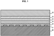
- the figure 1 illustrates a sectional view of the structure of such a sensor which comprises, in particular, the layers below deposited one after the other above an S0 support.
- Such an S0 support (for example a substrate) is made of PET or PEN or PI, or of the CIU type (ABF, FR4, etc.) or also of glass.
- the first layer 10 consists of a pattern of electrically conductive material (Au, Ag, Al, Cu) comprising metallic columns M1 and a ground line (not shown).
- the second layer 20 consists of a pyroelectric material composed of a PVDF copolymer (in English, “PolyVinyliDeneFluoride” for Polyvinylfluoride) and Trfe (trifluoroethylene) which covers the lines M1.
- PVDF copolymer in English, “PolyVinyliDeneFluoride” for Polyvinylfluoride”
- Trfe trifluoroethylene
- the third layer 30 is made of electrically conductive material and supports a fourth layer 40 of dielectric material itself supporting a fifth layer 50 comprising lines of electrically conductive material, preferably metallic, which will be heated.
- Each pixel is formed by a pyroelectric capacitance itself formed by two electrically and thermally conductive electrodes (but to a lesser extent in order to avoid a possible lateral thermal short circuit) (first and third layers 10, 30) between which a portion of pyroelectric material is arranged, and a heating element (layer 50).
- This heating element dissipates a certain amount of heat in the pixel, and the heating of the pixel is measured after a certain acquisition time, called integration time, in the presence of the finger on the sensor.
- such a sensor can be manufactured using various printing techniques or by subtractive methods such as photolithography, in particular with regard to obtaining the passive matrix of pixels. Not all printing techniques allow access to this device with the same cost. Also, there is a need to be able to implement liquid deposition techniques (in English, "slot die") which are inexpensive for manufacturing such a sensor.
- An object of the invention is to provide a pixel matrix of a thermal pattern sensor, which is a three-dimensional (3D) pattern, which can be obtained by means of a roll process (in English “roll to roll”) or sheet to sheet (in English, “sheet to sheet”) combined with techniques of printing / deposition of layers which are inexpensive.
- 3D three-dimensional
- the arrangement of the different layers of the pixel matrix makes it possible to implement simple and inexpensive techniques for manufacturing said layers.
- the layers made up of at least one strip of width preferably greater than or equal to 5 mm can be deposited by liquid means by means of a technique using a slit-shaped die through which the material to be deposited is brought to the surface in the form of ink.
- this technique is known as "slot die” or “slit coating”. This technique is very suitable when it comes to depositing continuous strips or long strips.
- the invention relates according to a second aspect to a pixel matrix of a thermal pattern sensor manufactured by a method as defined above.
- the invention relates according to a third aspect to a thermal pattern sensor comprising a matrix of pixels as defined above, the matrix being typically passive or active.
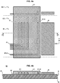
- the figure 2a illustrates a top view of a matrix of a thermal sensor according to an embodiment of the invention and the figure 2b illustrates a side view of an AA section of the motif of the figure 2a .
- roller printing in English "roll to roll"
- a roll comprising a continuous flow of supports is unwound for be brought to several printing stages.
- the advantage of roller printing is that it is faster than printing support by support and avoids handling operations to bring a support from one printing stage to another printing stage.
- roller printing allows you to handle very thin media. Indeed, the handling of the support by support requires a certain rigidity, whereas in the roller, the tension of the roller makes the supports very thin to handle.
- the matrix can be obtained by means of a printing or liquid deposition process in sheet-by-sheet mode.
- the matrix comprises a stack of several layers 100, 200, 300, 400, 500, 600 on a support S such as a substrate.
- the support S has a first edge s1, a second edge s2 and a rectangular upper surface s3 having a width along an axis X and a length along an axis Y.
- the support S is for example made of glass or a semiconductor material (such as Si).
- the support S has a thickness of between 25 and 200 microns, typically 50 to 125 microns.
- the support S is a flexible material, for example based on PI (polyimide) or PEN (polytethylene naphthalate) or PET (polyethylene terephthalate).
- the electrically conductive pattern is made of metallic material, typically gold, or a less precious metal (Silver, Aluminum or Copper, etc.).
- the thickness of the metallic pattern is between 50 and 200 nm.
- FIG. 2b is a section along the AA axis so that the connection tabs are not visible.
- This first layer is advantageously deposited by means of offset printing or by engraving or gravure printing or else by lithography or laser structuring. It will be noted that strips of constant width are deposited.
- the offset technique consists in that a cylinder comes to deposit the metal on a second cylinder which passes over the support S.
- the diameter of the roller must be correctly arranged to make regular patterns.
- This printing technique has the advantage of printing precise patterns.
- a second layer 200 (see the Figures 4a and 4b ), preferably comprising a rectangular strip 221, of pyroelectric material covering the tracks c 1 , c 2 , c 128 and leaving free at least part of the legs p 1 , p 2 , p 128 for connection.
- a pyroelectric material is for example P (VDF-TrFE) or PVDF.
- PVDF-TrFE PVDF
- Other variants can be envisaged for the choice of the material as soon as it is suitable for forming a pyroelectric capacity.
- the strip 221 is of constant width (rectangular on the figure 4a ) and covers the tracks c 1 , c 2 , c 128 but not all of the connection tabs p 1 , p 2 , p 128 which are left visible in order to be able to make connections / welds.
- the strip 221 made of pyroelectric material does not cover (even partially) the strip m of mass. Thus, possibly there is a space between the strip 221 of pyroelectric material and the rectangular mass strip m.
- the thickness of the second layer 200 is between 1 and 10 microns, preferably from 2 to 5 microns and even more preferably from 3 microns.
- This second layer 200 is advantageously deposited by liquid means by means of a slot die making a continuous strip in the direction of unwinding of the roll, or by making long strips in the case of a sheet mode. sheet, or a juxtaposition of several bands when several dies are manufactured in parallel.
- the strips extend between each cutting line, the rectangular shape being obtained after cutting the die.
- the layer of pyroelectric material can be deposited in two (or more) passes, or two successive layers to facilitate and obtain a more homogeneous deposit, especially when the final thickness becomes large, for example 5 microns.
- a third layer 300 (see the Figures 5a and 5b ) comprising a strip 331 of constant width of electrically conductive material straddling the strip 221 of pyroelectric material of the second layer and the mass strip m without completely covering the free part of the connection tabs of the first layer.
- This third layer is advantageously deposited by liquid means by means of a slot die making a continuous strip in the direction of unwinding of the roll or by making long strips in the case of a sheet-by-sheet mode. or a juxtaposition of several bands when several dies are produced in parallel.
- the strips extend between each cutting line, the rectangular shape being obtained after cutting the die.
- This third layer 300 constitutes an upper electrode for the sensor matrix and is typically made of PEDOT: PSS or of conductive ink based on silver.
- the strip 331 of the third layer 300 is connected to the strip m of ground. Again the legs p 1 , p 2 , p 128 of connections are left visible.
- part of the rectangular strip 221 of pyroelectric material is left visible along the first edge S1 of the support S after the deposition of the strip 331 of electrically conductive material.
- a space is provided in the second direction of elongation X along which the strip 221 of pyroelectric material remains visible.
- the thickness of the third layer is between 100 and 2000 nanometers, preferably less than 1000 nanometers and more precisely around 400 nm.
- a fourth layer 400 (see Figures 6a and 6b ) comprising a strip 441 of constant width of dielectric material in contact with the strip 221 of pyroelectric material of the second layer 200 and the strip 331 of metallic material of the third layer 300.
- the rectangular strip 441 of dielectric material is in contact with the third layer 300 and extends so as to cover the tracks of the first layer 100.
- This fourth layer 400 is advantageously deposited by liquid deposition by means of a slot die by making a continuous strip in the direction of unwinding of the roll or by making long strips in the case of a sheet by sheet mode or even a juxtaposition of several bands when several stamps are produced in parallel.
- the strips extend between each cutting line, the rectangular shape being obtained after cutting the die.
- a fifth layer 500 (see the Figures 7a and 7b ) comprising electrically conductive heating tracks w 1 , w 2 , w 128 arranged extending from the ground strip of the first layer towards the first edge of the support S of so as to cover the tracks of the first layer. These tracks constitute the lines of the pixel matrix.
- the heating tracks w 1 , w 2 , w 128 are connected to the ground strip and do not go beyond the connection tabs p 1 , p 128 .
- the electrically conductive heating tracks w 1 , w 2 , w 128 are connected to the upper electrode constituted by the third layer 300 or to the mass strip m. It is noted that in the case where the fourth layer 400 projects beyond the strip 331 of the third layer 300, the electrical contact is always ensured since the two layers are connected to the same ground strip.
- the electrically conductive heating tracks are made of metallic material, typically gold, or a less expensive metal (Silver, Aluminum or Copper, etc.).
- the thickness of the metal heating strips is between 20 and 2000 nm, typically 500 to 1000 nm. The choice of metal is unimportant, the main thing being to have a controlled resistance.
- This fifth layer 500 is advantageously deposited by means of offset printing or rotogravure or by metal vacuum deposition (PVD) associated with a photolithography or laser structuring means.
- PVD metal vacuum deposition
- a sixth layer 600 (see Figures 8a and 8b ) comprising a strip 661 of constant width of protection extending along the axis X from the strip m of mass towards the first edge s1 of the support S.
- the rectangular protective strip 661 is such that it leaves the connection tabs and the ends of the heating tracks w visible.
- the thickness of the rectangular protective strip must be optimized to protect the layers below while allowing heat to pass through.
- the thickness of the sixth layer is between 2 and 10 microns.
- This sixth layer 600 is advantageously deposited by liquid means by means of a slot die (“die die” by making a continuous strip in the direction of unwinding of the roll or by making long strips in the case of a sheet mode with sheet or a juxtaposition of several strips when several dies are manufactured in parallel
- a slot die by making a continuous strip in the direction of unwinding of the roll or by making long strips in the case of a sheet mode with sheet or a juxtaposition of several strips when several dies are manufactured in parallel
- the strips extend between each cutting line, the rectangular shape being obtained after cutting the pattern.
- this sixth layer 600 is advantageously made of material: DYMAX OC3021, DYMAX OC4122, PHC XH100, UVHC7300, UVL3.
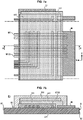
- the figure 9 illustrates a matrix according to a second embodiment.
- This second embodiment differs from the first embodiment by the arrangements of the tabs p 1 , p 128 for connecting the first layer 100.
- the tracks and the connection tabs of the first layer form an alternation of L and L turned over so that the connection tabs are partly above the electrically conductive heating tracks of the fifth layer and at below electrically conductive heating tracks in a direction Y of the support S.
- the first layer may further comprise a polarization POL strip connected to the tracks c 1 , c 128 .
- This polarization band POL is in this case printed between two matrixes of pixels M i , M i + 1 .
- the pyroelectric material For the pyroelectric material to acquire its pyroelectric properties, it must be polarized once and for all by subjecting it to an electric field of about 100 to 120 volts per micron of thickness of the pyroelectric material, for example 350 volts for 3 microns. . It is through the tracks of the first layer that the pyroelectric material of the second layer 120 directly above the columns of the first layer 110 will be polarized.
- the area comprising the polarization strip is cut out.
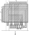
- the tracks c 1 , c 2 of the first layer are connected by means of metal strips b in areas which are intended to be cut, an area being located between two matrices of pixels M i , M i + 1 and the other zone, beyond the output edge (see the vertical cutting line on the left on the figure 12 ). It is noted that it is in this zone that the bias strip is printed.
- the electrically conductive heating tracks in addition to the first embodiment or to the second embodiment, provision is made for the electrically conductive heating tracks to terminate at the output edge with electrically conductive blocks w 1 ′ , w 2 ′ , w 128 ′ .
- the electrically conductive pavers are of the same material as that used for the first layer and produced at the same time as the latter.
- the rows and columns of the matrix exit through the output edge in a single metal which facilitates subsequent connections.
- the fourth layer 400 can be completely covered by the fifth layer 500 to protect it. This is particularly favorable in the case of a layer of silver to prevent its sulfurization.
- Such blocks are very advantageous when it comes to connecting the rows and columns of the matrix to a silicon chip 700 as illustrated in the figure 13 .
- the chip 700 is mounted as a flip-chip (upside-down chip), that is to say upside down with its contact pads downwards in front of the metal zones exiting through the output edge.
- the matrix thus described therefore has the advantage of being obtained by means of a roller printing technique comprising several stages of liquid deposition "slot die".
- connection tabs on one of the sides of the support S makes it possible to continuously print pixel arrays on a support S which travels from floor to floor.
Abstract
L'invention concerne un procédé de fabrication d'une matrice de pixels d'un capteur de motif thermique comprenant les étapes de :
fourniture d'un substrat ;
formation d'une première couche en matériau électriquement conducteur, comprenant un dépôt de pistes électriquement conductrices, un dépôt de pattes de connexion et un dépôt d'une bande de masse ;
formation d'une deuxième couche en matériau pyroélectrique recouvrant les pistes et laissant libre au moins une partie des pattes de connexion ;
formation d'une troisième couche en matériau électriquement conducteur ;
formation d'une quatrième couche en matériau diélectrique en contact avec la troisième couche ;
dépôt d'une cinquième couche comprenant des pistes électriquement conductrices chauffantes ;
dépôt d'une sixième couche de protection,
dans lequel le dépôt de la deuxième et/ou de la troisième et/ou de la quatrième et/ou de la sixième couche est mis en oeuvre par dépôt par voie liquide au moyen d'une filière à fente.

providing a substrate;
forming a first layer of electrically conductive material, comprising depositing electrically conductive tracks, depositing connection tabs and depositing a ground strip;
forming a second layer of pyroelectric material covering the tracks and leaving at least a portion of the connection tabs free;
forming a third layer of electrically conductive material;
forming a fourth layer of dielectric material in contact with the third layer;
depositing a fifth layer comprising electrically conductive heating tracks;
deposit of a sixth protective layer,
wherein the deposition of the second and / or the third and / or the fourth and / or the sixth layer is carried out by liquid deposition by means of a slit die.
Description
L'invention concerne un procédé de fabrication d'un capteur de motif thermique, par exemple un capteur d'empreintes digitales dit « actif », réalisant une détection thermique active ou passive et comprenant, de préférence, une matrice active ou passive de pixels. L'invention concerne plus particulièrement la fabrication de la matrice de pixels.The invention relates to a method for manufacturing a thermal pattern sensor, for example a so-called “active” fingerprint sensor, performing active or passive thermal detection and preferably comprising an active or passive matrix of pixels. The invention relates more particularly to the manufacture of the pixel matrix.
Un capteur d'empreintes digitales comporte des moyens de détection thermique. Ces moyens de détection thermique peuvent correspondre à des éléments pyroélectriques, des diodes, des thermistances ou tout autre élément sensible à la température permettant de convertir une variation de température en une variation de potentiel ou de courant électrique.A fingerprint sensor includes thermal detection means. These thermal detection means can correspond to pyroelectric elements, diodes, thermistors or any other element sensitive to the temperature making it possible to convert a variation in temperature into a variation in potential or electric current.
On connaît des documents
La
Un tel support S0 (par exemple un substrat) est en PET ou PEN ou PI, ou encore de type CIU (ABF, FR4, ...) ou encore en verre.Such an S0 support (for example a substrate) is made of PET or PEN or PI, or of the CIU type (ABF, FR4, etc.) or also of glass.
La première couche 10 est constituée par un motif en matériau conducteur électrique (Au, Ag, Al, Cu) comportant des colonnes M1 métalliques et une ligne de masse (non représentée).The
La deuxième couche 20 est constituée d'un matériau pyroélectrique composé d'un copolymère de PVDF (en anglais, « PolyVinyliDeneFluoride » pour Polyfluorure de Vinydilène) et de Trfe (trifluoroethylène) qui recouvre les lignes M1.The
La troisième couche 30 est en matériau conducteur électrique et supporte une quatrième couche 40 en matériau diélectrique elle-même supportant une cinquième couche 50 comportant des lignes en matériau conducteur électrique, de préférence métallique, qui vont être chauffées.The
Enfin une sixième couche 60 de protection recouvre l'ensemble.Finally a sixth
Chaque pixel est formé par une capacité pyroélectrique elle-même formée de deux électrodes conductrices électriquement et thermiquement (mais dans une moindre mesure afin d'éviter un éventuel court-circuit thermique latéral) (première et troisième couches 10, 30) entre lesquelles une portion de matériau pyroélectrique est disposée, et un élément chauffant (couche 50). Cet élément chauffant dissipe une certaine quantité de chaleur dans le pixel, et l'échauffement du pixel est mesuré au bout d'un certain temps d'acquisition, appelé temps d'intégration, en présence du doigt sur le capteur. Cela permet de distinguer, au niveau de chaque pixel, la présence d'une crête ou d'une vallée de l'empreinte détectée suivant que la chaleur est absorbée par la peau (pixel en présence d'une crête de l'empreinte) ou conservée dans le pixel (pixel en présence d'une vallée de l'empreinte). Cela conduit à une température finale plus faible dans le cas d'un pixel en présence d'une crête, où la chaleur est absorbée par la peau, par rapport à un pixel en présence d'une vallée.Each pixel is formed by a pyroelectric capacitance itself formed by two electrically and thermally conductive electrodes (but to a lesser extent in order to avoid a possible lateral thermal short circuit) (first and
De manière classique un tel capteur peut être fabriqué au moyen de diverses techniques d'impression ou par des méthodes soustractives comme la photolithographie notamment pour ce qui est de l'obtention de la matrice passive de pixels. Toutes les techniques d'impression ne permettent pas d'accéder à ce dispositif avec le même coût. Aussi, il existe un besoin de pouvoir mettre en oeuvre des techniques de dépôt par voie liquide (en anglais, « slot die ») qui sont peu coûteuses pour fabriquer un tel capteur.Conventionally, such a sensor can be manufactured using various printing techniques or by subtractive methods such as photolithography, in particular with regard to obtaining the passive matrix of pixels. Not all printing techniques allow access to this device with the same cost. Also, there is a need to be able to implement liquid deposition techniques (in English, "slot die") which are inexpensive for manufacturing such a sensor.
Un but de l'invention est de proposer une matrice de pixels d'un capteur de motif thermique, qui est un motif tridimensionnel (3D), pouvant être obtenue au moyen d'un procédé à rouleau (en anglais « roll to roll ») ou feuille à feuilles (en anglais, « sheet to sheet ») combiné à des techniques d'impression / dépôt des couches qui soient peu coûteuses.An object of the invention is to provide a pixel matrix of a thermal pattern sensor, which is a three-dimensional (3D) pattern, which can be obtained by means of a roll process (in English "roll to roll") or sheet to sheet (in English, "sheet to sheet") combined with techniques of printing / deposition of layers which are inexpensive.
A cet effet, l'invention propose selon un premier aspect un procédé de fabrication d'une matrice de pixels d'un capteur de motif thermique, le procédé comprenant les étapes de :
- fourniture d'un substrat ;
- formation d'une première couche en matériau électriquement conducteur, comprenant :
- ∘ un dépôt de pistes électriquement conductrices s'étendant selon une première direction d'allongement ;
- ∘ un dépôt de pattes de connexion, s'étendant depuis les pistes, selon une deuxième direction d'allongement, différente de la première direction d'allongement, et en se dirigeant vers un premier bord du substrat, dit bord de sortie ;
- ∘ un dépôt d'une bande de masse destinée à former la masse du capteur ;
formation d'une deuxième couche en matériau pyroélectrique recouvrant les pistes et laissant libre au moins une partie des pattes de connexion ;
formation d'une troisième couche en matériau électriquement conducteur déposée à cheval entre la couche de matériau pyroélectrique et la bande de masse sans recouvrir la partie libre des pattes de connexion ;
formation d'une quatrième couche en matériau diélectrique en contact avec la troisième couche et s'étendant de manière à recouvrir les pistes de la première couche ;
dépôt d'une cinquième couche comprenant des pistes électriquement conductrices chauffantes lesdites pistes électriquement conductrices chauffantes s'étendant depuis la bande de masse vers le premier bord du substrat de manière à recouvrir les pistes de la première couche ;
dépôt d'une sixième couche de protection ;
procédé de fabrication dans lequel le dépôt de la deuxième couche et/ou le dépôt de la troisième couche et/ou le dépôt de la quatrième couche et/ou le dépôt de la sixième couche est mis en oeuvre par dépôt par voie liquide au moyen d'une filière à fente.
- providing a substrate;
- formation of a first layer of electrically conductive material, comprising:
- ∘ a deposit of electrically conductive tracks extending in a first direction of elongation;
- ∘ a deposit of connection tabs, extending from the tracks, in a second direction of elongation, different from the first direction of elongation, and moving towards a first edge of the substrate, called the output edge;
- ∘ depositing a mass strip intended to form the mass of the sensor;
forming a second layer of pyroelectric material covering the tracks and leaving at least a portion of the connection tabs free;
forming a third layer of electrically conductive material deposited astride the layer of pyroelectric material and the ground strip without covering the free part of the connection tabs;
forming a fourth layer of dielectric material in contact with the third layer and extending so as to cover the tracks of the first layer;
depositing a fifth layer comprising electrically conductive heating tracks, said electrically conductive heating tracks extending from the ground strip towards the first edge of the substrate so as to cover the tracks of the first layer;
deposit of a sixth protective layer;
manufacturing process in which the deposition of the second layer and / or the deposition of the third layer and / or the deposition of the fourth layer and / or the deposition of the sixth layer is carried out by liquid deposition by means of 'a slotted die.
Les avantages de l'invention sont multiples.The advantages of the invention are manifold.
L'agencement des différentes couches de la matrice de pixels permet de mettre en oeuvre des techniques simples et peu coûteuses pour fabriquer lesdites couches.The arrangement of the different layers of the pixel matrix makes it possible to implement simple and inexpensive techniques for manufacturing said layers.
En effet, les couches constituées d'au moins une bande de largeur préférentiellement supérieure ou égale à 5 mm peuvent être déposées par voie liquide au moyen d'une technique mettant en oeuvre une filière en forme de fente au travers de laquelle le matériau à déposer est amené sur la surface sous forme d'encre. En anglais, cette technique est connue sous le terme « slot die » ou « slit coating ». Cette technique est très adaptée lorsqu'il s'agit de déposer des bandes continues ou de longues bandes.In fact, the layers made up of at least one strip of width preferably greater than or equal to 5 mm can be deposited by liquid means by means of a technique using a slit-shaped die through which the material to be deposited is brought to the surface in the form of ink. In English, this technique is known as "slot die" or "slit coating". This technique is very suitable when it comes to depositing continuous strips or long strips.
L'invention est avantageusement complétée par les caractéristiques suivantes, prises seules ou en une quelconque de leurs combinaisons techniquement possibles :
- les couches sont formées successivement de la manière suivante : formation de la première couche, formation de la deuxième couche, formation de la troisième couche, formation de la quatrième couche, formation de la cinquième couche, formation de la sixième couche ;
- les couches sont formées successivement de la manière suivante : formation de la cinquième couche, formation de la quatrième couche, formation de la première couche, formation de la deuxième couche, formation de la troisième couche, formation de la sixième couche ;
- la première couche comprend en outre une bande de polarisation connectée à des colonnes du motif métallique de la première couche ;
- les pistes de la première couche forment un serpentin, les pistes étant connectées deux à deux au moyen de bandelettes métalliques ;
- la première couche comprend en outre des pavés métalliques destinés à être dans le prolongement des pistes électriquement conductrices chauffantes de la cinquième couche ;
- les pistes et les pattes de connexions de la première couche forment une pluralité de L imbriqués les uns dans les autres ;
- à l'issue du procédé, les pattes de connexions sont toutes en-dessous des pistes électriquement conductrices chauffantes de la cinquième couche ;
- les pistes et les pattes de connexion de la première couche forment une alternance de L et de L retournés ;
- l'étape de formation de la troisième couche est mise en oeuvre de sorte à ménager un espace selon la deuxième direction d'allongement le long duquel la deuxième couche en matériau pyroélectrique reste apparente ;
- au cours de l'étape de formation de la deuxième couche, on réalise une juxtaposition de plusieurs bandes de matériau pyroélectrique afin de réaliser plusieurs matrices de pixels en parallèle.
- the layers are successively formed in the following manner: formation of the first layer, formation of the second layer, formation of the third layer, formation of the fourth layer, formation of the fifth layer, formation of the sixth layer;
- the layers are successively formed as follows: formation of the fifth layer, formation of the fourth layer, formation of the first layer, formation of the second layer, formation of the third layer, formation of the sixth layer;
- the first layer further comprises a polarization strip connected to columns of the metallic pattern of the first layer;
- the tracks of the first layer form a serpentine, the tracks being connected two by two by means of metal strips;
- the first layer further comprises metal blocks intended to be in the extension of the electrically conductive heating tracks of the fifth layer;
- the tracks and the connection tabs of the first layer form a plurality of L nested one inside the other;
- at the end of the process, the connection tabs are all below the electrically conductive heating tracks of the fifth layer;
- the tracks and the connection lugs of the first layer form an alternation of L and L returned;
- the step of forming the third layer is implemented so as to provide a space in the second direction of elongation along which the second layer of pyroelectric material remains visible;
- during the step of forming the second layer, a plurality of strips of pyroelectric material is juxtaposed in order to produce several matrixes of pixels in parallel.
L'invention se rapporte selon un deuxième aspect à une matrice de pixels d'un capteur de motif thermique fabriquée par un procédé tel que défini ci-avant.The invention relates according to a second aspect to a pixel matrix of a thermal pattern sensor manufactured by a method as defined above.
L'invention concerne selon un troisième aspect un capteur de motif thermique comprenant une matrice de pixels telle que définie ci-avant, la matrice étant typiquement passive ou active.The invention relates according to a third aspect to a thermal pattern sensor comprising a matrix of pixels as defined above, the matrix being typically passive or active.
D'autres caractéristiques, buts et avantages de l'invention ressortiront de la description qui suit, qui est purement illustrative et non limitative, et qui doit être lue en regard des dessins annexés sur lesquels, outre la
- la
figure 2a illustre une vue de dessus d'une matrice de pixels selon un premier mode de réalisation de l'invention ; - la
figure 2b illustre une vue de côté en coupe de la matrice de lafigure 2a ; - les
figures 3a à 8b illustrent le dépôt des couches successives au cours d'un procédé de fabrication d'une matrice de pixels selon l'invention. - la
figure 9 illustre une vue de dessus d'une matrice de pixels selon un deuxième mode de réalisation ; - la
figure 10 illustre une vue de dessus d'une matrice de pixels selon un mode de réalisation complémentaire au premier mode de réalisation ; - la
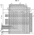
figure 11 illustre une vue dessus d'une matrice de pixels selon un mode de réalisation complémentaire au premier mode de réalisation ; - la
figure 12 illustre une vue de dessus d'une matrice de pixels selon un mode de réalisation complémentaire au premier mode de réalisation ou au second mode de réalisation ; - la
figure 13 illustre une vue de dessus d'une matrice de pixels selon un mode complémentaire mode de réalisation de lafigure 12 .
- the
figure 2a illustrates a top view of a pixel matrix according to a first embodiment of the invention; - the
figure 2b illustrates a side view in section of the matrix of thefigure 2a ; - the
Figures 3a to 8b illustrate the deposition of successive layers during a process for manufacturing a pixel matrix according to the invention. - the
figure 9 illustrates a top view of a pixel matrix according to a second embodiment; - the
figure 10 illustrates a top view of a pixel matrix according to an embodiment complementary to the first embodiment; - the
figure 11 illustrates a top view of a matrix of pixels according to an embodiment complementary to the first embodiment; - the
figure 12 illustrates a top view of a pixel matrix according to an embodiment complementary to the first embodiment or to the second embodiment; - the
figure 13 illustrates a top view of a pixel matrix according to a complementary embodiment of thefigure 12 .
Sur l'ensemble des figures les éléments similaires portent des références identiques.In all of the figures, similar elements bear identical references.
La
Sur cette figure, on voit un motif complet Mi et le début du motif suivant Mi+1, les deux étant séparés sur la figure par un trait épais en pointillés (il s'agit en fait d'une ligne imaginaire de découpe selon laquelle à l'issue de toutes les étapes de fabrication la matrice sera découpée selon cette ligne).In this figure, we see a complete pattern Mi and the beginning of the following pattern M i + 1 , the two being separated in the figure by a thick dashed line (it is actually an imaginary cutting line according to which at the end of all the manufacturing stages the die will be cut along this line).
En effet, selon un mode de réalisation préféré, et dans ce qui suit, on se place dans le cas d'une impression à rouleaux (en anglais « roll to roll ») selon laquelle un rouleau comprenant un flux continu de supports est déroulé pour être amené à plusieurs étages d'impression. L'intérêt de l'impression à rouleau est qu'elle est plus rapide qu'une impression support par support et évite les opérations de manipulation pour amener un support d'un étage d'impression à un autre étage d'impression.Indeed, according to a preferred embodiment, and in what follows, we place ourselves in the case of a roller printing (in English "roll to roll") according to which a roll comprising a continuous flow of supports is unwound for be brought to several printing stages. The advantage of roller printing is that it is faster than printing support by support and avoids handling operations to bring a support from one printing stage to another printing stage.
En outre, l'impression à rouleaux permet de manipuler des supports très minces. En effet la manipulation support par support exige une certaine rigidité alors qu'en rouleau, la tension du rouleau rend des supports très minces manipulables.In addition, roller printing allows you to handle very thin media. Indeed, the handling of the support by support requires a certain rigidity, whereas in the roller, the tension of the roller makes the supports very thin to handle.
On comprendra que plusieurs matrices peuvent êtres obtenues sur la largeur d'un seul rouleau, la largeur étant mesurée selon une direction sensiblement perpendiculaire à une direction de déroulement du rouleau. Le rouleau de support doit alors présenter une largeur suffisante pour réaliser une juxtaposition de plusieurs bandes.It will be understood that several dies can be obtained over the width of a single roll, the width being measured in a direction substantially perpendicular to a direction of unwinding of the roll. The support roll must then have a sufficient width to make a juxtaposition of several strips.
Bien entendu, on comprend que la matrice peut être obtenue au moyen d'un procédé d'impression ou de dépôt par voie liquide en mode feuille à feuille.Of course, it is understood that the matrix can be obtained by means of a printing or liquid deposition process in sheet-by-sheet mode.
En outre, on va décrire ci-après la fabrication d'une matrice.In addition, the manufacture of a matrix will be described below.
Toutefois,comme indiqué ci-avant, plusieurs matrices peuvent être obtenues en parallèle sur la largeur du support, conditionnellement à la largeur des rouleaux sur lesquels est enroulé le support. En relation avec les
Cet empilement n'est pas limitatif comme on le verra par la suite.This stacking is not limiting as will be seen later.
Le support S présente un premier bord s1, un deuxième bord s2 et une surface s3 supérieure rectangulaire ayant une largeur selon un axe X et une longueur selon un axe Y.The support S has a first edge s1, a second edge s2 and a rectangular upper surface s3 having a width along an axis X and a length along an axis Y.
Le support S est par exemple en verre ou en matériau semiconducteur (tel que du Si). En outre, le support S présente une épaisseur comprise entre 25 et 200 microns, typiquement 50 à 125 microns.The support S is for example made of glass or a semiconductor material (such as Si). In addition, the support S has a thickness of between 25 and 200 microns, typically 50 to 125 microns.
De préférence, et afin d'être compatible avec un procédé d'impression ou de dépôt par voie liquide par rouleau, le support S est un matériau souple par exemple à base de PI (polyimide) ou de PEN (polytéthylène naphtalate) ou de PET (polyéthylène téréphtalate).Preferably, and in order to be compatible with a printing or liquid deposition process by roller, the support S is a flexible material, for example based on PI (polyimide) or PEN (polytethylene naphthalate) or PET (polyethylene terephthalate).
Sur ce support S plusieurs couches sont déposées, typiquement par des techniques de dépôt en voie liquide qui seront décrites plus loin.On this support S several layers are deposited, typically by liquid deposition techniques which will be described later.
Une première couche 100 comprend un motif conducteur électrique (voir les
- Des pistes formant des colonnes c1, c2, c128 de la matrice de pixels et qui constituent l'électrode inférieure. Ces pistes sont parallèles entre elles selon une première direction d'allongement (selon l'axe Y). Typiquement la matrice comprend 128 pistes.
- Des pattes p1, p2, p128 de connexion, s'étendant depuis les pistes, selon une deuxième direction d'allongement (selon l'axe X), et en se dirigeant vers un premier bord du substrat S dit bord de sortie (c'est à-dire le bord par lequel les connexions/soudures seront effectuées).
- une bande m de masse parallèle aux pistes et s'étendant le long d'un second bord opposé au premier bord (selon l'axe Y) ;
- Tracks forming columns c 1 , c 2 , c 128 of the pixel matrix and which constitute the lower electrode. These tracks are mutually parallel in a first direction of elongation (along the Y axis). Typically the matrix includes 128 tracks.
- Connection lugs p 1 , p 2 , p 128 , extending from the tracks, in a second direction of elongation (along the X axis), and moving towards a first edge of the substrate S called the output edge (i.e. the edge through which the connections / welds will be made).
- a strip m of mass parallel to the tracks and extending along a second edge opposite the first edge (along the Y axis);
Le motif conducteur électrique est en matériau métallique, typiquement de l'or, ou un métal moins précieux (Argent, Aluminium ou Cuivre, etc.). L'épaisseur du motif métallique est comprise entre 50 et 200 nm.The electrically conductive pattern is made of metallic material, typically gold, or a less precious metal (Silver, Aluminum or Copper, etc.). The thickness of the metallic pattern is between 50 and 200 nm.
A noter que la
Cette première couche est avantageusement déposée au moyen d'une impression par offset ou par gravure ou héliogravure ou bien encore par lithographie ou structuration laser. On remarquera que sont déposées des bandes de largeur constante.This first layer is advantageously deposited by means of offset printing or by engraving or gravure printing or else by lithography or laser structuring. It will be noted that strips of constant width are deposited.
La technique par offset consiste en ce qu'un cylindre vient déposer le métal sur un second cylindre qui passe sur le support S. Bien entendu le diamètre du rouleau doit être correctement agencé pour faire des motifs réguliers. Cette technique d'impression présente l'avantage d'imprimer des motifs précis.The offset technique consists in that a cylinder comes to deposit the metal on a second cylinder which passes over the support S. Of course the diameter of the roller must be correctly arranged to make regular patterns. This printing technique has the advantage of printing precise patterns.
Une deuxième couche 200 (voir les
Un matériau pyroélectrique est par exemple du P(VDF-TrFE) ou du PVDF. D'autres variantes peuvent être envisagées pour le choix du matériau dès lors qu'il est adapté pour former une capacité pyroélectrique.A pyroelectric material is for example P (VDF-TrFE) or PVDF. Other variants can be envisaged for the choice of the material as soon as it is suitable for forming a pyroelectric capacity.
Comme visible sur la
A titre d'exemple, l'épaisseur de la deuxième couche 200 (matériau pyroélectrique) est comprise entre 1 et 10 microns de préférence de 2 à 5 microns et encore plus préférentiellement de 3 microns.For example, the thickness of the second layer 200 (pyroelectric material) is between 1 and 10 microns, preferably from 2 to 5 microns and even more preferably from 3 microns.
Cette deuxième couche 200 est avantageusement déposée par voie liquide au moyen d'une filière à fente (« slot die ») réalisant une bande continue dans la direction de déroulement du rouleau, ou en réalisant de longues bandes dans le cas d'un mode feuille à feuille, ou encore une juxtaposition de plusieurs bandes lorsque plusieurs matrices sont fabriquées en parallèle. De préférence, au cours de l'étape de dépôt les bandes s'étendent entre chaque ligne de découpe, la forme rectangulaire étant obtenue après découpe de la matrice.This
Optionnellement, la couche de matériau pyroélectrique peut être déposée en deux (ou plus) passes, ou deux couches successives pour faciliter et obtenir un dépôt plus homogène, surtout lorsque l'épaisseur finale devient importante, par exemple 5 microns.Optionally, the layer of pyroelectric material can be deposited in two (or more) passes, or two successive layers to facilitate and obtain a more homogeneous deposit, especially when the final thickness becomes large, for example 5 microns.
Une troisième couche 300 (voir les
Comme visible la
De préférence, une partie de la bande rectangulaire 221 en matériau pyroélectrique est laissée apparente le long du premier bord S1 du support S à l'issue du dépôt de la bande 331 en matériau conducteur électrique. On ménage un espace selon la deuxième direction d'allongement X le long duquel la bande 221 en matériau pyroélectrique reste apparente.Preferably, part of the
A titre d'exemple, l'épaisseur de la troisième couche est comprise entre 100 et 2000 nanomètres, de préférence inférieure à 1000 nanomètres et plus précisément autour de 400 nm.For example, the thickness of the third layer is between 100 and 2000 nanometers, preferably less than 1000 nanometers and more precisely around 400 nm.
Une quatrième couche 400 (voir les
La bande 441 rectangulaire en matériau diélectrique est en contact avec la troisième couche 300 et s'étend de manière à recouvrir les pistes de la première couche 100.The
Cette quatrième couche 400 est avantageusement déposée par dépôt par voie liquide au moyen d'une filière à fente (« slot die ») en réalisant une bande continue dans la direction de déroulement du rouleau ou en réalisant de longues bandes dans le cas d'un mode feuille à feuille ou encore une juxtaposition de plusieurs bandes lorsque plusieurs matricés sont fabriquées en parallèle. De préférence, au cours de l'étape de dépôt les bandes s'étendent entre chaque ligne de découpe, la forme rectangulaire étant obtenue après découpe de la matrice.This
Une cinquième couche 500 (voir les
Les pistes w1, w2, w128 de chauffage sont connectées à la bande de masse et ne vont pas au-delà des pattes p1, p128 de connexion. En outre, les pistes w1, w2, w128 électriquement conductrices de chauffage sont connectées à l'électrode supérieure constituée par la troisième couche 300 ou à la bande de masse m. On note que dans le cas où la quatrième couche 400 déborde de la bande 331 de la troisième couche 300 le contact électrique est toujours assuré puisque les deux couches sont reliées à la même bande de masse.The heating tracks w 1 , w 2 , w 128 are connected to the ground strip and do not go beyond the connection tabs p 1 , p 128 . In addition, the electrically conductive heating tracks w 1 , w 2 , w 128 are connected to the upper electrode constituted by the
A titre d'exemple, les pistes électriquement conductrices de chauffage sont en matériau métallique, typiquement de l'or, ou un métal moins cher (Argent, Aluminium ou Cuivre, etc.). L'épaisseur des bandes métalliques de chauffage est comprise entre 20 et 2000 nm, typiquement 500 à 1000 nm. Le choix du métal est peu important, l'essentiel étant d'avoir une résistance contrôlée.For example, the electrically conductive heating tracks are made of metallic material, typically gold, or a less expensive metal (Silver, Aluminum or Copper, etc.). The thickness of the metal heating strips is between 20 and 2000 nm, typically 500 to 1000 nm. The choice of metal is unimportant, the main thing being to have a controlled resistance.
Cette cinquième couche 500 est avantageusement déposée au moyen d'une impression par offset ou par héliogravure ou par dépôt sous vide de metal (PVD) associé à un moyen de photolithographie ou de structuration laser.This
Une sixième couche 600 (voir les
La bande 661 rectangulaire de protection est telle qu'elle laisse apparente les pattes de connexion et les extrémités des pistes de chauffage w.The rectangular
L'épaisseur de la bande rectangulaire de protection doit être optimisée pour protéger les couches au-dessous tout en laissant passer la chaleur.The thickness of the rectangular protective strip must be optimized to protect the layers below while allowing heat to pass through.
Par exemple, l'épaisseur de la sixième couche est comprise entre 2 et 10 microns.For example, the thickness of the sixth layer is between 2 and 10 microns.
Cette sixième couche 600 est avantageusement déposée par voie liquide au moyen d'une filière à fente (« slot die » en réalisant une bande continue dans la direction de déroulement du rouleau ou en réalisant de longues bandes dans le cas d'un mode feuille à feuille ou encore une juxtaposition de plusieurs bandes lorsque plusieurs matrices sont fabriquées en parallèle. De préférence, au cours de l'étape de dépôt les bandes s'étendent entre chaque ligne de découpe, la forme rectangulaire étant obtenue après découpe du motif.This
En outre, cette sixième couche 600 est avantageusement en matériau : DYMAX OC3021, DYMAX OC4122, PHC XH100, UVHC7300, UVL3.In addition, this
La
Ce deuxième mode de réalisation diffère du premier mode de réalisation par les dispositions des pattes p1, p128 de connexion de la première couche 100.This second embodiment differs from the first embodiment by the arrangements of the tabs p 1 , p 128 for connecting the
En particulier, les pistes et les pattes de connexion de la première couche forment une alternance de L et de L retournés de telle sorte que les pattes de connexions sont pour une partie au-dessus des pistes électriquement conductrices de chauffage de la cinquième couche et au-dessous des pistes électriquement conductrices de chauffage selon une direction Y du support S.In particular, the tracks and the connection tabs of the first layer form an alternation of L and L turned over so that the connection tabs are partly above the electrically conductive heating tracks of the fifth layer and at below electrically conductive heating tracks in a direction Y of the support S.
En relation avec la
En effet, pour que le matériau pyroélectrique acquière ses propriétés pyroélectriques il faut le polariser une bonne fois pour toute en le soumettant un champ électrique d'environ 100 à 120 volts par micron d'épaisseur du matériau pyroélectrique, par exemple 350 volts pour 3 microns. C'est par l'intermédiaire des pistes de la première couche que le matériau pyroélectrique de la deuxième couche 120 directement au-dessus des colonnes de la première couche 110 va être polarisé.In fact, for the pyroelectric material to acquire its pyroelectric properties, it must be polarized once and for all by subjecting it to an electric field of about 100 to 120 volts per micron of thickness of the pyroelectric material, for example 350 volts for 3 microns. . It is through the tracks of the first layer that the pyroelectric material of the second layer 120 directly above the columns of the first layer 110 will be polarized.
En outre, on prévoit dans ce mode de réalisation de la
Une fois le matériau pyroélectrique polarisé la zone comportant la bande de polarisation est découpée.Once the pyroelectric material has been polarized, the area comprising the polarization strip is cut out.
Toujours pour des questions de polarisation, en relation avec la
Grâce à cette disposition de la
En relation avec la
De tels pavés sont très avantageux lorsqu'il s'agira de connecter les lignes et les colonnes de la matrice à une puce 700 en silicium comme illustré sur la
Avantageusement, le procédé de fabrication de la matrice comprend dont les étapes suivantes mises en oeuvre successivement :
- dépôt E1 de la première couche comprenant le dépôt des pistes, le dépôt des pattes de connexion et le dépôt de la bande de masse ;
- dépôt E2 de la deuxième couche ;
- dépôt E3 de la troisième couche ;
- dépôt E4 de la quatrième couche ;
- dépôt E5 de la cinquième couche ;
- dépôt E6 de la sixième couche.
- deposition E1 of the first layer comprising the deposition of the tracks, the deposition of the connection lugs and the deposition of the ground strip;
- deposition E2 of the second layer;
- deposit E3 of the third layer;
- deposit E4 of the fourth layer;
- deposit E5 of the fifth layer;
- deposit E6 of the sixth layer.
Selon une deuxième de fabrication, le procédé de fabrication de la matrice comprend dont les étapes suivantes mises en oeuvre successivement :
- dépôt E5 de la cinquième couche ;
- dépôt E4 de la quatrième couche ;
- dépôt E1 de la première couche comprenant le dépôt des pistes, le dépôt des pattes de connexion et le dépôt de la bande de masse ;
- dépôt E2 de la deuxième couche ;
- dépôt E3 de la troisième couche ;
- dépôt E6 de la sixième couche.
- deposit E5 of the fifth layer;
- deposit E4 of the fourth layer;
- deposition E1 of the first layer comprising the deposition of the tracks, the deposition of the connection lugs and the deposition of the ground strip;
- deposition E2 of the second layer;
- deposit E3 of the third layer;
- deposit E6 of the sixth layer.
La matrice ainsi décrite présente donc l'avantage d'être obtenue au moyen d'une technique d'impression à rouleaux comprenant plusieurs étages de dépôt par voie liquide « slot die ».The matrix thus described therefore has the advantage of being obtained by means of a roller printing technique comprising several stages of liquid deposition "slot die".
En outre, le fait de prévoir les pattes de connexion sur un des côtés du support S permet d'imprimer en flux continu des matrices de pixels sur un support S qui chemine d'étage à étage.In addition, the fact of providing the connection tabs on one of the sides of the support S makes it possible to continuously print pixel arrays on a support S which travels from floor to floor.
Claims (13)
procédé de fabrication dans lequel le dépôt de la deuxième couche (200) et/ou le dépôt de la troisième couche et/ou le dépôt de la quatrième couche et/ou le dépôt de la sixième couche est mis en oeuvre par dépôt par voie liquide au moyen d'une filière à fente.
manufacturing process in which the deposition of the second layer (200) and / or the deposition of the third layer and / or the deposition of the fourth layer and / or the deposition of the sixth layer is carried out by liquid deposition by means of a slotted die.
Applications Claiming Priority (1)
| Application Number | Priority Date | Filing Date | Title |
|---|---|---|---|
| FR1857511A FR3085078B1 (en) | 2018-08-16 | 2018-08-16 | METHOD FOR MANUFACTURING A PIXEL MATRIX OF A THERMAL PATTERN SENSOR AND ASSOCIATED SENSOR |
Publications (2)
| Publication Number | Publication Date |
|---|---|
| EP3611660A1 true EP3611660A1 (en) | 2020-02-19 |
| EP3611660B1 EP3611660B1 (en) | 2022-03-09 |
Family
ID=65494235
Family Applications (1)
| Application Number | Title | Priority Date | Filing Date |
|---|---|---|---|
| EP19306017.5A Active EP3611660B1 (en) | 2018-08-16 | 2019-08-14 | Method of manufacturing an array of pixels from a thermal pattern sensor and associated sensor |
Country Status (3)
| Country | Link |
|---|---|
| US (1) | US10949638B2 (en) |
| EP (1) | EP3611660B1 (en) |
| FR (1) | FR3085078B1 (en) |
Citations (3)
| Publication number | Priority date | Publication date | Assignee | Title |
|---|---|---|---|---|
| US6091837A (en) | 1995-04-11 | 2000-07-18 | Dinh; Ngoc Minh | Sensor for acquiring a fingerprint image based on heat transfer |
| EP2385486A1 (en) | 2010-05-06 | 2011-11-09 | Commissariat à l'Énergie Atomique et aux Énergies Alternatives | Transducer for temporal variation of temperature, electronic chip including transducteur and method for manufacturing chip |
| WO2018020176A1 (en) | 2016-07-29 | 2018-02-01 | Commissariat A L'energie Atomique Et Aux Energies Alternatives | Active thermal pattern sensor comprising a passive matrix of pixels |
Family Cites Families (1)
| Publication number | Priority date | Publication date | Assignee | Title |
|---|---|---|---|---|
| FR3044408B1 (en) * | 2015-11-30 | 2019-06-14 | Commissariat A L'energie Atomique Et Aux Energies Alternatives | THERMAL PATTERN SENSOR WITH HORIZONTAL PYROELECTRIC CAPABILITY |
-
2018
- 2018-08-16 FR FR1857511A patent/FR3085078B1/en active Active
-
2019
- 2019-08-14 EP EP19306017.5A patent/EP3611660B1/en active Active
- 2019-08-15 US US16/542,236 patent/US10949638B2/en active Active
Patent Citations (3)
| Publication number | Priority date | Publication date | Assignee | Title |
|---|---|---|---|---|
| US6091837A (en) | 1995-04-11 | 2000-07-18 | Dinh; Ngoc Minh | Sensor for acquiring a fingerprint image based on heat transfer |
| EP2385486A1 (en) | 2010-05-06 | 2011-11-09 | Commissariat à l'Énergie Atomique et aux Énergies Alternatives | Transducer for temporal variation of temperature, electronic chip including transducteur and method for manufacturing chip |
| WO2018020176A1 (en) | 2016-07-29 | 2018-02-01 | Commissariat A L'energie Atomique Et Aux Energies Alternatives | Active thermal pattern sensor comprising a passive matrix of pixels |
Non-Patent Citations (1)
| Title |
|---|
| XIAOYU DING ET AL: "A review of the operating limits in slot die coating processes", AICHE JOURNAL, vol. 62, no. 7, 4 May 2016 (2016-05-04), US, pages 2508 - 2524, XP055591404, ISSN: 0001-1541, DOI: 10.1002/aic.15268 * |
Also Published As
| Publication number | Publication date |
|---|---|
| FR3085078A1 (en) | 2020-02-21 |
| EP3611660B1 (en) | 2022-03-09 |
| US20200057879A1 (en) | 2020-02-20 |
| FR3085078B1 (en) | 2020-07-17 |
| US10949638B2 (en) | 2021-03-16 |
Similar Documents
| Publication | Publication Date | Title |
|---|---|---|
| FR3044408B1 (en) | THERMAL PATTERN SENSOR WITH HORIZONTAL PYROELECTRIC CAPABILITY | |
| FR3035220A1 (en) | "ELECTRONIC DEVICE FOR MEASURING AT LEAST ONE ELECTRICAL CHARACTERISTIC OF AN OBJECT" | |
| WO2008125446A2 (en) | Photovoltaic device with discontinuous interdigited heterojunction structure | |
| EP2836896B1 (en) | Touch sensor and a fabrication method therefor | |
| EP0126110B1 (en) | Thermal flowmeter with thermocouples | |
| WO2018020176A1 (en) | Active thermal pattern sensor comprising a passive matrix of pixels | |
| FR3044409A1 (en) | THERMAL PATTERN SENSOR COMPRISING A HIGH PYROELECTRIC PORTION WITH HIGH THERMAL CONDUCTIVITY | |
| FR2988912A1 (en) | ENERGY RECOVERY DEVICE | |
| EP1524507A1 (en) | Bolometer, infra-red detection apparatus using it and means of manufacture | |
| CA2712381C (en) | Method for making a heating element by depositing thin layers onto an insulating substrate, and resulting element | |
| FR3069938A1 (en) | THERMO-RESISTIVE CAPSULE CAPTURE DEVICE ADAPTED TO PASSIVE ADDRESSING | |
| EP3611660B1 (en) | Method of manufacturing an array of pixels from a thermal pattern sensor and associated sensor | |
| EP3502638B1 (en) | Pyroelectric sensor with electromagnetic shielding comprising a composite material | |
| EP3492892A1 (en) | Thermal pattern sensor with pyroelectric capacity | |
| EP3502639A1 (en) | Pyroelectric sensor with improved electromagnetic shielding | |
| EP3640615B1 (en) | Pyroelectric sensor with improved coating for abrasion resistance | |
| EP3492894A1 (en) | Thermal pattern sensor with pyroelectric capacity | |
| FR2779274A1 (en) | INTEGRATED CIRCUIT WITH STOP LAYER AND MANUFACTURING METHOD THEREOF | |
| WO2006077342A1 (en) | Method for metallisation of a semiconductor device | |
| EP3767261B1 (en) | Thermal pattern sensor with pixel matrix with heating lines in coil | |
| EP2567418B1 (en) | Microelectronic device having disconnected semiconductor portions and method for producing such a device | |
| EP3979334A1 (en) | Encapsulation for solar module with integrated connection elements | |
| WO2016027028A1 (en) | Device for obtaining fingerprints | |
| FR3093802A1 (en) | THERMAL PATTERN SENSOR | |
| FR3107989A1 (en) | THERMAL PATTERN SENSOR WHOSE SURFACIC PROTECTIVE LAYER PRESENTS ANISOTROPIC THERMAL CONDUCTION |
Legal Events
| Date | Code | Title | Description |
|---|---|---|---|
| PUAI | Public reference made under article 153(3) epc to a published international application that has entered the european phase |
Free format text: ORIGINAL CODE: 0009012 |
|
| STAA | Information on the status of an ep patent application or granted ep patent |
Free format text: STATUS: THE APPLICATION HAS BEEN PUBLISHED |
|
| AK | Designated contracting states |
Kind code of ref document: A1 Designated state(s): AL AT BE BG CH CY CZ DE DK EE ES FI FR GB GR HR HU IE IS IT LI LT LU LV MC MK MT NL NO PL PT RO RS SE SI SK SM TR |
|
| AX | Request for extension of the european patent |
Extension state: BA ME |
|
| STAA | Information on the status of an ep patent application or granted ep patent |
Free format text: STATUS: REQUEST FOR EXAMINATION WAS MADE |
|
| 17P | Request for examination filed |
Effective date: 20200630 |
|
| RBV | Designated contracting states (corrected) |
Designated state(s): AL AT BE BG CH CY CZ DE DK EE ES FI FR GB GR HR HU IE IS IT LI LT LU LV MC MK MT NL NO PL PT RO RS SE SI SK SM TR |
|
| STAA | Information on the status of an ep patent application or granted ep patent |
Free format text: STATUS: EXAMINATION IS IN PROGRESS |
|
| 17Q | First examination report despatched |
Effective date: 20200929 |
|
| STAA | Information on the status of an ep patent application or granted ep patent |
Free format text: STATUS: EXAMINATION IS IN PROGRESS |
|
| GRAP | Despatch of communication of intention to grant a patent |
Free format text: ORIGINAL CODE: EPIDOSNIGR1 |
|
| STAA | Information on the status of an ep patent application or granted ep patent |
Free format text: STATUS: GRANT OF PATENT IS INTENDED |
|
| INTG | Intention to grant announced |
Effective date: 20211123 |
|
| GRAS | Grant fee paid |
Free format text: ORIGINAL CODE: EPIDOSNIGR3 |
|
| GRAA | (expected) grant |
Free format text: ORIGINAL CODE: 0009210 |
|
| STAA | Information on the status of an ep patent application or granted ep patent |
Free format text: STATUS: THE PATENT HAS BEEN GRANTED |
|
| AK | Designated contracting states |
Kind code of ref document: B1 Designated state(s): AL AT BE BG CH CY CZ DE DK EE ES FI FR GB GR HR HU IE IS IT LI LT LU LV MC MK MT NL NO PL PT RO RS SE SI SK SM TR |
|
| REG | Reference to a national code |
Ref country code: CH Ref legal event code: EP Ref country code: AT Ref legal event code: REF Ref document number: 1474773 Country of ref document: AT Kind code of ref document: T Effective date: 20220315 |
|
| REG | Reference to a national code |
Ref country code: DE Ref legal event code: R096 Ref document number: 602019012335 Country of ref document: DE |
|
| REG | Reference to a national code |
Ref country code: IE Ref legal event code: FG4D Free format text: LANGUAGE OF EP DOCUMENT: FRENCH |
|
| REG | Reference to a national code |
Ref country code: LT Ref legal event code: MG9D |
|
| REG | Reference to a national code |
Ref country code: NL Ref legal event code: MP Effective date: 20220309 |
|
| PG25 | Lapsed in a contracting state [announced via postgrant information from national office to epo] |
Ref country code: SE Free format text: LAPSE BECAUSE OF FAILURE TO SUBMIT A TRANSLATION OF THE DESCRIPTION OR TO PAY THE FEE WITHIN THE PRESCRIBED TIME-LIMIT Effective date: 20220309 Ref country code: RS Free format text: LAPSE BECAUSE OF FAILURE TO SUBMIT A TRANSLATION OF THE DESCRIPTION OR TO PAY THE FEE WITHIN THE PRESCRIBED TIME-LIMIT Effective date: 20220309 Ref country code: NO Free format text: LAPSE BECAUSE OF FAILURE TO SUBMIT A TRANSLATION OF THE DESCRIPTION OR TO PAY THE FEE WITHIN THE PRESCRIBED TIME-LIMIT Effective date: 20220609 Ref country code: LT Free format text: LAPSE BECAUSE OF FAILURE TO SUBMIT A TRANSLATION OF THE DESCRIPTION OR TO PAY THE FEE WITHIN THE PRESCRIBED TIME-LIMIT Effective date: 20220309 Ref country code: HR Free format text: LAPSE BECAUSE OF FAILURE TO SUBMIT A TRANSLATION OF THE DESCRIPTION OR TO PAY THE FEE WITHIN THE PRESCRIBED TIME-LIMIT Effective date: 20220309 Ref country code: BG Free format text: LAPSE BECAUSE OF FAILURE TO SUBMIT A TRANSLATION OF THE DESCRIPTION OR TO PAY THE FEE WITHIN THE PRESCRIBED TIME-LIMIT Effective date: 20220609 |
|
| REG | Reference to a national code |
Ref country code: AT Ref legal event code: MK05 Ref document number: 1474773 Country of ref document: AT Kind code of ref document: T Effective date: 20220309 |
|
| PG25 | Lapsed in a contracting state [announced via postgrant information from national office to epo] |
Ref country code: LV Free format text: LAPSE BECAUSE OF FAILURE TO SUBMIT A TRANSLATION OF THE DESCRIPTION OR TO PAY THE FEE WITHIN THE PRESCRIBED TIME-LIMIT Effective date: 20220309 Ref country code: GR Free format text: LAPSE BECAUSE OF FAILURE TO SUBMIT A TRANSLATION OF THE DESCRIPTION OR TO PAY THE FEE WITHIN THE PRESCRIBED TIME-LIMIT Effective date: 20220610 Ref country code: FI Free format text: LAPSE BECAUSE OF FAILURE TO SUBMIT A TRANSLATION OF THE DESCRIPTION OR TO PAY THE FEE WITHIN THE PRESCRIBED TIME-LIMIT Effective date: 20220309 |
|
| PG25 | Lapsed in a contracting state [announced via postgrant information from national office to epo] |
Ref country code: NL Free format text: LAPSE BECAUSE OF FAILURE TO SUBMIT A TRANSLATION OF THE DESCRIPTION OR TO PAY THE FEE WITHIN THE PRESCRIBED TIME-LIMIT Effective date: 20220309 |
|
| PG25 | Lapsed in a contracting state [announced via postgrant information from national office to epo] |
Ref country code: SM Free format text: LAPSE BECAUSE OF FAILURE TO SUBMIT A TRANSLATION OF THE DESCRIPTION OR TO PAY THE FEE WITHIN THE PRESCRIBED TIME-LIMIT Effective date: 20220309 Ref country code: SK Free format text: LAPSE BECAUSE OF FAILURE TO SUBMIT A TRANSLATION OF THE DESCRIPTION OR TO PAY THE FEE WITHIN THE PRESCRIBED TIME-LIMIT Effective date: 20220309 Ref country code: RO Free format text: LAPSE BECAUSE OF FAILURE TO SUBMIT A TRANSLATION OF THE DESCRIPTION OR TO PAY THE FEE WITHIN THE PRESCRIBED TIME-LIMIT Effective date: 20220309 Ref country code: PT Free format text: LAPSE BECAUSE OF FAILURE TO SUBMIT A TRANSLATION OF THE DESCRIPTION OR TO PAY THE FEE WITHIN THE PRESCRIBED TIME-LIMIT Effective date: 20220711 Ref country code: ES Free format text: LAPSE BECAUSE OF FAILURE TO SUBMIT A TRANSLATION OF THE DESCRIPTION OR TO PAY THE FEE WITHIN THE PRESCRIBED TIME-LIMIT Effective date: 20220309 Ref country code: EE Free format text: LAPSE BECAUSE OF FAILURE TO SUBMIT A TRANSLATION OF THE DESCRIPTION OR TO PAY THE FEE WITHIN THE PRESCRIBED TIME-LIMIT Effective date: 20220309 Ref country code: CZ Free format text: LAPSE BECAUSE OF FAILURE TO SUBMIT A TRANSLATION OF THE DESCRIPTION OR TO PAY THE FEE WITHIN THE PRESCRIBED TIME-LIMIT Effective date: 20220309 Ref country code: AT Free format text: LAPSE BECAUSE OF FAILURE TO SUBMIT A TRANSLATION OF THE DESCRIPTION OR TO PAY THE FEE WITHIN THE PRESCRIBED TIME-LIMIT Effective date: 20220309 |
|
| REG | Reference to a national code |
Ref country code: DE Ref legal event code: R079 Ref document number: 602019012335 Country of ref document: DE Free format text: PREVIOUS MAIN CLASS: G06K0009000000 Ipc: G06V0010000000 |
|
| PG25 | Lapsed in a contracting state [announced via postgrant information from national office to epo] |
Ref country code: PL Free format text: LAPSE BECAUSE OF FAILURE TO SUBMIT A TRANSLATION OF THE DESCRIPTION OR TO PAY THE FEE WITHIN THE PRESCRIBED TIME-LIMIT Effective date: 20220309 Ref country code: IS Free format text: LAPSE BECAUSE OF FAILURE TO SUBMIT A TRANSLATION OF THE DESCRIPTION OR TO PAY THE FEE WITHIN THE PRESCRIBED TIME-LIMIT Effective date: 20220709 Ref country code: AL Free format text: LAPSE BECAUSE OF FAILURE TO SUBMIT A TRANSLATION OF THE DESCRIPTION OR TO PAY THE FEE WITHIN THE PRESCRIBED TIME-LIMIT Effective date: 20220309 |
|
| REG | Reference to a national code |
Ref country code: DE Ref legal event code: R097 Ref document number: 602019012335 Country of ref document: DE |
|
| PLBE | No opposition filed within time limit |
Free format text: ORIGINAL CODE: 0009261 |
|
| STAA | Information on the status of an ep patent application or granted ep patent |
Free format text: STATUS: NO OPPOSITION FILED WITHIN TIME LIMIT |
|
| PG25 | Lapsed in a contracting state [announced via postgrant information from national office to epo] |
Ref country code: DK Free format text: LAPSE BECAUSE OF FAILURE TO SUBMIT A TRANSLATION OF THE DESCRIPTION OR TO PAY THE FEE WITHIN THE PRESCRIBED TIME-LIMIT Effective date: 20220309 |
|
| 26N | No opposition filed |
Effective date: 20221212 |
|
| PG25 | Lapsed in a contracting state [announced via postgrant information from national office to epo] |
Ref country code: SI Free format text: LAPSE BECAUSE OF FAILURE TO SUBMIT A TRANSLATION OF THE DESCRIPTION OR TO PAY THE FEE WITHIN THE PRESCRIBED TIME-LIMIT Effective date: 20220309 |
|
| PG25 | Lapsed in a contracting state [announced via postgrant information from national office to epo] |
Ref country code: MC Free format text: LAPSE BECAUSE OF FAILURE TO SUBMIT A TRANSLATION OF THE DESCRIPTION OR TO PAY THE FEE WITHIN THE PRESCRIBED TIME-LIMIT Effective date: 20220309 |
|
| REG | Reference to a national code |
Ref country code: CH Ref legal event code: PL |
|
| PG25 | Lapsed in a contracting state [announced via postgrant information from national office to epo] |
Ref country code: LU Free format text: LAPSE BECAUSE OF NON-PAYMENT OF DUE FEES Effective date: 20220814 Ref country code: LI Free format text: LAPSE BECAUSE OF NON-PAYMENT OF DUE FEES Effective date: 20220831 Ref country code: CH Free format text: LAPSE BECAUSE OF NON-PAYMENT OF DUE FEES Effective date: 20220831 |
|
| REG | Reference to a national code |
Ref country code: BE Ref legal event code: MM Effective date: 20220831 |
|
| PG25 | Lapsed in a contracting state [announced via postgrant information from national office to epo] |
Ref country code: IT Free format text: LAPSE BECAUSE OF FAILURE TO SUBMIT A TRANSLATION OF THE DESCRIPTION OR TO PAY THE FEE WITHIN THE PRESCRIBED TIME-LIMIT Effective date: 20220309 Ref country code: IE Free format text: LAPSE BECAUSE OF NON-PAYMENT OF DUE FEES Effective date: 20220814 |
|
| PG25 | Lapsed in a contracting state [announced via postgrant information from national office to epo] |
Ref country code: BE Free format text: LAPSE BECAUSE OF NON-PAYMENT OF DUE FEES Effective date: 20220831 |
|
| PGFP | Annual fee paid to national office [announced via postgrant information from national office to epo] |
Ref country code: FR Payment date: 20230821 Year of fee payment: 5 Ref country code: DE Payment date: 20230822 Year of fee payment: 5 |
|
| PG25 | Lapsed in a contracting state [announced via postgrant information from national office to epo] |
Ref country code: HU Free format text: LAPSE BECAUSE OF FAILURE TO SUBMIT A TRANSLATION OF THE DESCRIPTION OR TO PAY THE FEE WITHIN THE PRESCRIBED TIME-LIMIT; INVALID AB INITIO Effective date: 20190814 |