EP3609063A1 - Power conversion device - Google Patents
Power conversion device Download PDFInfo
- Publication number
- EP3609063A1 EP3609063A1 EP17904816.0A EP17904816A EP3609063A1 EP 3609063 A1 EP3609063 A1 EP 3609063A1 EP 17904816 A EP17904816 A EP 17904816A EP 3609063 A1 EP3609063 A1 EP 3609063A1
- Authority
- EP
- European Patent Office
- Prior art keywords
- terminal
- secondary winding
- conversion device
- power conversion
- smoothing
- Prior art date
- Legal status (The legal status is an assumption and is not a legal conclusion. Google has not performed a legal analysis and makes no representation as to the accuracy of the status listed.)
- Granted
Links
Images



Classifications
-
- H—ELECTRICITY
- H01—ELECTRIC ELEMENTS
- H01F—MAGNETS; INDUCTANCES; TRANSFORMERS; SELECTION OF MATERIALS FOR THEIR MAGNETIC PROPERTIES
- H01F27/00—Details of transformers or inductances, in general
- H01F27/28—Coils; Windings; Conductive connections
- H01F27/2847—Sheets; Strips
-
- H—ELECTRICITY
- H01—ELECTRIC ELEMENTS
- H01F—MAGNETS; INDUCTANCES; TRANSFORMERS; SELECTION OF MATERIALS FOR THEIR MAGNETIC PROPERTIES
- H01F27/00—Details of transformers or inductances, in general
- H01F27/28—Coils; Windings; Conductive connections
- H01F27/2847—Sheets; Strips
- H01F27/2852—Construction of conductive connections, of leads
-
- H—ELECTRICITY
- H02—GENERATION; CONVERSION OR DISTRIBUTION OF ELECTRIC POWER
- H02M—APPARATUS FOR CONVERSION BETWEEN AC AND AC, BETWEEN AC AND DC, OR BETWEEN DC AND DC, AND FOR USE WITH MAINS OR SIMILAR POWER SUPPLY SYSTEMS; CONVERSION OF DC OR AC INPUT POWER INTO SURGE OUTPUT POWER; CONTROL OR REGULATION THEREOF
- H02M3/00—Conversion of DC power input into DC power output
- H02M3/22—Conversion of DC power input into DC power output with intermediate conversion into AC
- H02M3/24—Conversion of DC power input into DC power output with intermediate conversion into AC by static converters
- H02M3/28—Conversion of DC power input into DC power output with intermediate conversion into AC by static converters using discharge tubes with control electrode or semiconductor devices with control electrode to produce the intermediate AC
-
- H—ELECTRICITY
- H02—GENERATION; CONVERSION OR DISTRIBUTION OF ELECTRIC POWER
- H02M—APPARATUS FOR CONVERSION BETWEEN AC AND AC, BETWEEN AC AND DC, OR BETWEEN DC AND DC, AND FOR USE WITH MAINS OR SIMILAR POWER SUPPLY SYSTEMS; CONVERSION OF DC OR AC INPUT POWER INTO SURGE OUTPUT POWER; CONTROL OR REGULATION THEREOF
- H02M3/00—Conversion of DC power input into DC power output
- H02M3/22—Conversion of DC power input into DC power output with intermediate conversion into AC
- H02M3/24—Conversion of DC power input into DC power output with intermediate conversion into AC by static converters
- H02M3/28—Conversion of DC power input into DC power output with intermediate conversion into AC by static converters using discharge tubes with control electrode or semiconductor devices with control electrode to produce the intermediate AC
- H02M3/325—Conversion of DC power input into DC power output with intermediate conversion into AC by static converters using discharge tubes with control electrode or semiconductor devices with control electrode to produce the intermediate AC using devices of a triode or a transistor type requiring continuous application of a control signal
- H02M3/335—Conversion of DC power input into DC power output with intermediate conversion into AC by static converters using discharge tubes with control electrode or semiconductor devices with control electrode to produce the intermediate AC using devices of a triode or a transistor type requiring continuous application of a control signal using semiconductor devices only
- H02M3/33569—Conversion of DC power input into DC power output with intermediate conversion into AC by static converters using discharge tubes with control electrode or semiconductor devices with control electrode to produce the intermediate AC using devices of a triode or a transistor type requiring continuous application of a control signal using semiconductor devices only having several active switching elements
- H02M3/33576—Conversion of DC power input into DC power output with intermediate conversion into AC by static converters using discharge tubes with control electrode or semiconductor devices with control electrode to produce the intermediate AC using devices of a triode or a transistor type requiring continuous application of a control signal using semiconductor devices only having several active switching elements having at least one active switching element at the secondary side of an isolation transformer
- H02M3/33592—Conversion of DC power input into DC power output with intermediate conversion into AC by static converters using discharge tubes with control electrode or semiconductor devices with control electrode to produce the intermediate AC using devices of a triode or a transistor type requiring continuous application of a control signal using semiconductor devices only having several active switching elements having at least one active switching element at the secondary side of an isolation transformer having a synchronous rectifier circuit or a synchronous freewheeling circuit at the secondary side of an isolation transformer
-
- H—ELECTRICITY
- H02—GENERATION; CONVERSION OR DISTRIBUTION OF ELECTRIC POWER
- H02M—APPARATUS FOR CONVERSION BETWEEN AC AND AC, BETWEEN AC AND DC, OR BETWEEN DC AND DC, AND FOR USE WITH MAINS OR SIMILAR POWER SUPPLY SYSTEMS; CONVERSION OF DC OR AC INPUT POWER INTO SURGE OUTPUT POWER; CONTROL OR REGULATION THEREOF
- H02M7/00—Conversion of AC power input into DC power output; Conversion of DC power input into AC power output
- H02M7/003—Constructional details, e.g. physical layout, assembly, wiring or busbar connections
-
- H—ELECTRICITY
- H02—GENERATION; CONVERSION OR DISTRIBUTION OF ELECTRIC POWER
- H02M—APPARATUS FOR CONVERSION BETWEEN AC AND AC, BETWEEN AC AND DC, OR BETWEEN DC AND DC, AND FOR USE WITH MAINS OR SIMILAR POWER SUPPLY SYSTEMS; CONVERSION OF DC OR AC INPUT POWER INTO SURGE OUTPUT POWER; CONTROL OR REGULATION THEREOF
- H02M7/00—Conversion of AC power input into DC power output; Conversion of DC power input into AC power output
- H02M7/02—Conversion of AC power input into DC power output without possibility of reversal
- H02M7/04—Conversion of AC power input into DC power output without possibility of reversal by static converters
- H02M7/06—Conversion of AC power input into DC power output without possibility of reversal by static converters using discharge tubes without control electrode or semiconductor devices without control electrode
-
- H—ELECTRICITY
- H02—GENERATION; CONVERSION OR DISTRIBUTION OF ELECTRIC POWER
- H02M—APPARATUS FOR CONVERSION BETWEEN AC AND AC, BETWEEN AC AND DC, OR BETWEEN DC AND DC, AND FOR USE WITH MAINS OR SIMILAR POWER SUPPLY SYSTEMS; CONVERSION OF DC OR AC INPUT POWER INTO SURGE OUTPUT POWER; CONTROL OR REGULATION THEREOF
- H02M3/00—Conversion of DC power input into DC power output
- H02M3/22—Conversion of DC power input into DC power output with intermediate conversion into AC
- H02M3/24—Conversion of DC power input into DC power output with intermediate conversion into AC by static converters
- H02M3/28—Conversion of DC power input into DC power output with intermediate conversion into AC by static converters using discharge tubes with control electrode or semiconductor devices with control electrode to produce the intermediate AC
- H02M3/325—Conversion of DC power input into DC power output with intermediate conversion into AC by static converters using discharge tubes with control electrode or semiconductor devices with control electrode to produce the intermediate AC using devices of a triode or a transistor type requiring continuous application of a control signal
- H02M3/335—Conversion of DC power input into DC power output with intermediate conversion into AC by static converters using discharge tubes with control electrode or semiconductor devices with control electrode to produce the intermediate AC using devices of a triode or a transistor type requiring continuous application of a control signal using semiconductor devices only
- H02M3/33569—Conversion of DC power input into DC power output with intermediate conversion into AC by static converters using discharge tubes with control electrode or semiconductor devices with control electrode to produce the intermediate AC using devices of a triode or a transistor type requiring continuous application of a control signal using semiconductor devices only having several active switching elements
- H02M3/33573—Full-bridge at primary side of an isolation transformer
-
- Y—GENERAL TAGGING OF NEW TECHNOLOGICAL DEVELOPMENTS; GENERAL TAGGING OF CROSS-SECTIONAL TECHNOLOGIES SPANNING OVER SEVERAL SECTIONS OF THE IPC; TECHNICAL SUBJECTS COVERED BY FORMER USPC CROSS-REFERENCE ART COLLECTIONS [XRACs] AND DIGESTS
- Y02—TECHNOLOGIES OR APPLICATIONS FOR MITIGATION OR ADAPTATION AGAINST CLIMATE CHANGE
- Y02B—CLIMATE CHANGE MITIGATION TECHNOLOGIES RELATED TO BUILDINGS, e.g. HOUSING, HOUSE APPLIANCES OR RELATED END-USER APPLICATIONS
- Y02B70/00—Technologies for an efficient end-user side electric power management and consumption
- Y02B70/10—Technologies improving the efficiency by using switched-mode power supplies [SMPS], i.e. efficient power electronics conversion e.g. power factor correction or reduction of losses in power supplies or efficient standby modes
Definitions
- the present invention relates to the structure of a power conversion device for use in, for example, electric vehicles, plug-in hybrid vehicles, or trains.
- One known power conversion device is a DC/DC converter equipped with a transformer, a rectifier element, a smoothing coil, and a smoothing capacitor.
- the rectifier element is connected to a secondary winding of the transformer, and the smoothing coil and the smoothing capacitor are provided to smoothen an output voltage.
- a typical circuit example of the DC/DC converter includes a configuration in which a MOSFET, a smoothing coil, and a smoothing capacitor are used to form a choke input LC filter (see Patent Literature 1, for example).
- the path may be made shorter.
- a terminal of the secondary winding, to which the rectifier element is connected is arranged between the smoothing coil and a connection portion at which to connect the intermediate terminal and a base member.
- the smoothing coil and the connection portion at which to connect the intermediate terminal and the base member it is difficult to shorten the path between the smoothing coil and the connection portion at which to connect the intermediate terminal and the base member.
- the present invention has been made with a view to solving the above-mentioned problem, and the present invention provides a power conversion device having a high output smoothing property that is obtained by shortening a path from a connection portion between a smoothing coil and a smoothing capacitor via the smoothing capacitor to a ground portion corresponding to an intermediate terminal of the transfer, at which the smoothing capacitor and the transformer are grounded.
- a power conversion device including, on a base: a transformer; a first rectifier element; a second rectifier element; a smoothing coil; and a smoothing capacitor
- the transformer including a secondary winding including a first secondary winding and a second secondary winding, and an intermediate terminal at which to connect the secondary winding and the base
- the smoothing coil including a smoothing coil first terminal and a smoothing coil second terminal
- the first rectifier element being connected to a first terminal formed at one end side of the first secondary winding and to the smoothing coil first terminal
- the second rectifier element being connected to a second terminal formed at one end side of the second secondary winding and to the smoothing coil first terminal
- the smoothing capacitor being connected to the smoothing coil second terminal and the intermediate terminal, another end side of the first secondary winding and another end side of the second secondary winding being connected to each other at a connection portion, the connection portion being located between the first terminal and the second terminal, and the first terminal or the second terminal being located between the intermediate terminal
- a power conversion device having a high output smoothing property that is obtained by shortening a path from the smoothing coil to the intermediate terminal of the transformer.
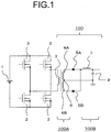
- FIG. 1 is a circuit diagram for illustrating a DC/DC converter for use in electrically powered vehicles such as an electric vehicle, a plug-in hybrid vehicle, or a train.
- the DC/DC converter is equipped with a power conversion device according to a first embodiment of the present invention.
- FIG. 2 is a perspective view for illustrating the power conversion device of the first embodiment.
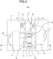
- FIG. 3 is a plan view for illustrating the power conversion device of the first embodiment.
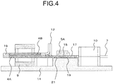
- FIG. 4 is a sectional view of the power conversion device taken along the line IV-IV of FIG. 3 .
- FIG. 5 is a view for illustrating the power conversion device of FIG. 2 , from which transformer cores and smoothing coil cores are removed.
- FIG. 6 is a view for illustrating the power conversion device of FIG. 5 , from which a resin portion is removed.
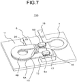
- FIG. 7 is a view for illustrating the power conversion device of FIG. 6 , from which a smoothing capacitor and a screw are removed.
- the DC/DC converter includes a DC power supply 1, a plurality of MOSFETs 2, and a power conversion device 100.
- the power conversion device 100 includes a transformer 100A including a primary winding 3, a first secondary winding 4A and a second secondary winding 4B, a pair of diodes 5A and 5B forming a rectifier circuit, and a choke input LC filter 100B including a smoothing coil 7 and a smoothing capacitor 8.
- the DC power supply 1 which is mounted on an electrically powered vehicle, supplies high-voltage power to a switching circuit configured by the plurality of MOSFETs 2 to generate an AC voltage.
- the generated AC voltage is applied to the primary winding 3 of the transformer 100A.
- the transformer 100A steps down the voltage in accordance with a turn ratio .
- the stepped-down voltage is applied to the first secondary winding 4A and the second secondary winding 4B of the transformer 100A, and then converted by the diodes 5A and 5B into a DC current including a pulsating current.
- the pulsating current is removed by a smoothing circuit including the smoothing coil 7 and the smoothing capacitor 8, and the resultant current is then supplied to an in-vehicle lead battery and an in-vehicle auxiliary battery device via an output terminal (not illustrated).
- the power conversion device 100 of the first embodiment includes, on a base 11, the transformer 100A including the first secondary winding 4A and the second secondary winding 4B that are covered by a pair of transformer cores 9.
- the power conversion device 100 further includes the pair of diodes 5A and 5B as rectifier elements, the smoothing coil 7 covered with a pair of smoothing coil cores 10, and the smoothing capacitor 8. Note that, the primary winding 3 as a part of the transformer 100A is not illustrated.
- the secondary winding of the transformer 100A is formed such that the second secondary winding 4B is placed on the first secondary winding 4A with a certain space therefrom, and is integrally molded through use of a resin 19.
- the resultant one is covered by the pair of transformer cores 9 from above and below.
- connection portion 12 On a first terminal 15 formed at one end side of the first secondary winding 4A, an anode of the diode 5A is surface-mounted by soldering. Meanwhile, on a second terminal 16 formed at one end side of the second secondary winding 4B, an anode of the diode 5B is surface-mounted by soldering. Another end side of the first secondary winding 4A and another end side of the second secondary winding 4B are welded to form a connection portion 12.
- the first secondary winding 4A, the second secondary winding 4B, and the smoothing coil 7 are integrally molded through use of the resin 19.
- the first terminal 15 of the first secondary winding 4A, the second terminal 16 of the second secondary winding 4B, and a smoothing coil first terminal 17 are each exposed from the resin 19.
- the first terminal 15 of the first secondary winding 4A, the second terminal 16 of the second secondary winding 4B, and the smoothing coil first terminal 17 are brought into contact with the base 11 through an insulating sheet 21, at their surfaces on which the diodes 5A and 5B are not mounted. With this arrangement, heat generated by the diodes 5A and 5B is transferred to the base 11 to be released.
- connection portion 12 between the first secondary winding 4A and the second secondary winding 4B is located between the first terminal 15 and the second terminal 16. Further, cathodes of the diodes 5A and 5B are surface-mounted by soldering to the smoothing coil first terminal 17.
- an intermediate terminal 6 is formed so as to extend from the first secondary winding 4A.
- the intermediate terminal 6 is provided opposite to the connection portion 12 across the second terminal 16. Further, the intermediate terminal 6 is connected to a boss 20 formed on the base 11 by means of a screw 14a, together with one terminal 8a of the smoothing capacitor 8.
- Another terminal 8b of the smoothing capacitor 8 is connected to a smoothing coil second terminal 18 by means of a screw 14b.
- the one terminal 8a of the smoothing capacitor 8 is directly connected to the intermediate terminal 6 extending from the first secondary winding 4A, and the another terminal 8b thereof is directly connected to the smoothing coil second terminal 18.
- This structure allows shortening of a path from the smoothing coil second terminal 18 via the smoothing capacitor 8 to the intermediate terminal 6. It is accordingly possible to reduce an impedance in the path and allow the LC filter 100B to sufficiently exert its functions, so as to achieve the power conversion device 100 having a high output smoothing property.
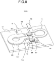
- FIG. 8 is a perspective view for illustrating a power conversion device 200 according to a second embodiment of the present invention, in which only the base 11, the first secondary winding 4A, the second secondary winding 4B, the smoothing coil 7, and the diodes 5A and 5B are illustrated.
- the power conversion device 200 of the second embodiment differs from the first embodiment in terms of a connection form of the first secondary winding 4A and the second secondary winding 4B. Other components are the same as those of the first embodiment.
- the first secondary winding 4A and the second secondary winding 4B of the power conversion device 200 are integrally produced by bending a single metal sheet at a portion corresponding to a bent portion 12a.
- aprocess for welding the first secondary winding 4A and the second secondary winding 4B can be omitted.
- the LC filter 100B can sufficiently exert its functions in the thus-simplified structure, so as to achieve the power conversion device 200 having a high output smoothing property.
- 1 DC power supply 2 MOSFET, 3 primary winding, 4A first secondary winding, 4B second secondary winding, 5A diode (first rectifier element), 5B diode (second rectifier element), 6 intermediate terminal, 7 smoothing coil, 8 smoothing capacitor, 8a, 8b terminal, 9 transformer core, 10 smoothing coil core, 11 base, 12 connection portion, 12a bent portion, 14a, 14b screw (fastening member), 15 first terminal, 16 second terminal, 17 smoothing coil first terminal, 18 smoothing coil second terminal, 19 resin, 20 boss, 21 insulating sheet, 100, 200 power conversion device, 100A transformer, 100B LC filter
Landscapes
- Engineering & Computer Science (AREA)
- Power Engineering (AREA)
- Dc-Dc Converters (AREA)
Abstract
Description
- The present invention relates to the structure of a power conversion device for use in, for example, electric vehicles, plug-in hybrid vehicles, or trains.
- One known power conversion device is a DC/DC converter equipped with a transformer, a rectifier element, a smoothing coil, and a smoothing capacitor. In this device, the rectifier element is connected to a secondary winding of the transformer, and the smoothing coil and the smoothing capacitor are provided to smoothen an output voltage. A typical circuit example of the DC/DC converter includes a configuration in which a MOSFET, a smoothing coil, and a smoothing capacitor are used to form a choke input LC filter (see Patent Literature 1, for example).
- In order to sufficiently exert function of the LC filter to smoothen an output of the device, it is important to reduce an impedance in a path from a connection portion between the smoothing coil and the smoothing capacitor via the smoothing capacitor to a ground portion corresponding to an intermediate terminal of the transformer, at which the smoothing capacitor and the transformer are grounded, so as to promote charging/discharging of the smoothing capacitor. As one approach to reducing impedance in the path from the smoothing coil to the intermediate terminal of the transformer, the path may be made shorter.
- [PTL 1]
JP 5933673 B1 - However, in the related-art power conversion device, a terminal of the secondary winding, to which the rectifier element is connected, is arranged between the smoothing coil and a connection portion at which to connect the intermediate terminal and a base member. Hence, it is difficult to shorten the path between the smoothing coil and the connection portion at which to connect the intermediate terminal and the base member.
- The present invention has been made with a view to solving the above-mentioned problem, and the present invention provides a power conversion device having a high output smoothing property that is obtained by shortening a path from a connection portion between a smoothing coil and a smoothing capacitor via the smoothing capacitor to a ground portion corresponding to an intermediate terminal of the transfer, at which the smoothing capacitor and the transformer are grounded.
- According to one embodiment of the present invention, there is provided a power conversion device including, on a base: a transformer; a first rectifier element; a second rectifier element; a smoothing coil; and a smoothing capacitor, the transformer including a secondary winding including a first secondary winding and a second secondary winding, and an intermediate terminal at which to connect the secondary winding and the base, the smoothing coil including a smoothing coil first terminal and a smoothing coil second terminal, the first rectifier element being connected to a first terminal formed at one end side of the first secondary winding and to the smoothing coil first terminal, the second rectifier element being connected to a second terminal formed at one end side of the second secondary winding and to the smoothing coil first terminal, the smoothing capacitor being connected to the smoothing coil second terminal and the intermediate terminal, another end side of the first secondary winding and another end side of the second secondary winding being connected to each other at a connection portion, the connection portion being located between the first terminal and the second terminal, and the first terminal or the second terminal being located between the intermediate terminal and the connection portion.
- According to one embodiment of the present invention, it is possible to provide a power conversion device having a high output smoothing property that is obtained by shortening a path from the smoothing coil to the intermediate terminal of the transformer.
-
-
FIG. 1 is a circuit diagram for illustrating a DC/DC converter equipped with a power conversion device according to a first embodiment of the present invention. -
FIG. 2 is a perspective view for illustrating the power conversion device according to the first embodiment of the present invention. -
FIG. 3 is a plan view for illustrating the power conversion device according to the first embodiment of the present invention. -
FIG. 4 is a sectional view of the power conversion device taken along the line IV-IV ofFIG. 3 . -
FIG. 5 is a view for illustrating the power conversion device ofFIG. 2 , from which transformer cores are removed. -
FIG. 6 is a view for illustrating the power conversion device ofFIG. 5 , from which a resin portion is removed. -
FIG. 7 is a view for illustrating the power conversion device ofFIG. 6 , from which a smoothing capacitor and a screw are removed. -
FIG. 8 is a view for illustrating a base, a secondary winding, rectifier elements, and a smoothing coil in a power conversion device according to a second embodiment of the present invention. - Now, with reference to the drawings, a power conversion device according to exemplary embodiments of the present invention is described.
-
FIG. 1 is a circuit diagram for illustrating a DC/DC converter for use in electrically powered vehicles such as an electric vehicle, a plug-in hybrid vehicle, or a train. The DC/DC converter is equipped with a power conversion device according to a first embodiment of the present invention.FIG. 2 is a perspective view for illustrating the power conversion device of the first embodiment.FIG. 3 is a plan view for illustrating the power conversion device of the first embodiment.FIG. 4 is a sectional view of the power conversion device taken along the line IV-IV ofFIG. 3 .FIG. 5 is a view for illustrating the power conversion device ofFIG. 2 , from which transformer cores and smoothing coil cores are removed.FIG. 6 is a view for illustrating the power conversion device ofFIG. 5 , from which a resin portion is removed.FIG. 7 is a view for illustrating the power conversion device ofFIG. 6 , from which a smoothing capacitor and a screw are removed. - As illustrated in
FIG. 1 , the DC/DC converter includes a DC power supply 1, a plurality ofMOSFETs 2, and apower conversion device 100. Thepower conversion device 100 includes atransformer 100A including aprimary winding 3, a firstsecondary winding 4A and a secondsecondary winding 4B, a pair ofdiodes input LC filter 100B including asmoothing coil 7 and asmoothing capacitor 8. - The DC power supply 1, which is mounted on an electrically powered vehicle, supplies high-voltage power to a switching circuit configured by the plurality of
MOSFETs 2 to generate an AC voltage. The generated AC voltage is applied to theprimary winding 3 of thetransformer 100A. Thetransformer 100A steps down the voltage in accordance with a turn ratio . The stepped-down voltage is applied to the firstsecondary winding 4A and the secondsecondary winding 4B of thetransformer 100A, and then converted by thediodes smoothing coil 7 and thesmoothing capacitor 8, and the resultant current is then supplied to an in-vehicle lead battery and an in-vehicle auxiliary battery device via an output terminal (not illustrated). - As illustrated in
FIG. 2 , thepower conversion device 100 of the first embodiment includes, on abase 11, thetransformer 100A including the firstsecondary winding 4A and the second secondary winding 4B that are covered by a pair oftransformer cores 9. Thepower conversion device 100 further includes the pair ofdiodes smoothing coil 7 covered with a pair ofsmoothing coil cores 10, and thesmoothing capacitor 8. Note that, theprimary winding 3 as a part of thetransformer 100A is not illustrated. - As illustrated in
FIG. 2 to FIG. 5 , the secondary winding of thetransformer 100A is formed such that the secondsecondary winding 4B is placed on the firstsecondary winding 4A with a certain space therefrom, and is integrally molded through use of aresin 19. The resultant one is covered by the pair oftransformer cores 9 from above and below. - On a
first terminal 15 formed at one end side of the firstsecondary winding 4A, an anode of thediode 5A is surface-mounted by soldering. Meanwhile, on asecond terminal 16 formed at one end side of the second secondary winding 4B, an anode of thediode 5B is surface-mounted by soldering. Another end side of the first secondary winding 4A and another end side of the second secondary winding 4B are welded to form aconnection portion 12. - The first
secondary winding 4A, the second secondary winding 4B, and thesmoothing coil 7 are integrally molded through use of theresin 19. Thefirst terminal 15 of the firstsecondary winding 4A, thesecond terminal 16 of the second secondary winding 4B, and a smoothing coilfirst terminal 17 are each exposed from theresin 19. - Further, as illustrated in
FIG. 4 , thefirst terminal 15 of the firstsecondary winding 4A, thesecond terminal 16 of the second secondary winding 4B, and the smoothing coilfirst terminal 17 are brought into contact with thebase 11 through aninsulating sheet 21, at their surfaces on which thediodes diodes base 11 to be released. - The
connection portion 12 between the firstsecondary winding 4A and the secondsecondary winding 4B is located between thefirst terminal 15 and thesecond terminal 16. Further, cathodes of thediodes first terminal 17. - As illustrated in
FIG. 6 andFIG. 7 , anintermediate terminal 6 is formed so as to extend from the firstsecondary winding 4A. Theintermediate terminal 6 is provided opposite to theconnection portion 12 across thesecond terminal 16. Further, theintermediate terminal 6 is connected to aboss 20 formed on thebase 11 by means of ascrew 14a, together with oneterminal 8a of thesmoothing capacitor 8. Another terminal 8b of thesmoothing capacitor 8 is connected to a smoothing coilsecond terminal 18 by means of ascrew 14b. - As described above, according to the
power conversion device 100 of the first embodiment, the oneterminal 8a of thesmoothing capacitor 8 is directly connected to theintermediate terminal 6 extending from the firstsecondary winding 4A, and theanother terminal 8b thereof is directly connected to the smoothing coilsecond terminal 18. This structure allows shortening of a path from the smoothing coilsecond terminal 18 via thesmoothing capacitor 8 to theintermediate terminal 6. It is accordingly possible to reduce an impedance in the path and allow theLC filter 100B to sufficiently exert its functions, so as to achieve thepower conversion device 100 having a high output smoothing property. -
FIG. 8 is a perspective view for illustrating apower conversion device 200 according to a second embodiment of the present invention, in which only thebase 11, the first secondary winding 4A, the second secondary winding 4B, the smoothingcoil 7, and thediodes power conversion device 200 of the second embodiment differs from the first embodiment in terms of a connection form of the first secondary winding 4A and the second secondary winding 4B. Other components are the same as those of the first embodiment. - As illustrated in
FIG. 8 , the first secondary winding 4A and the second secondary winding 4B of thepower conversion device 200 are integrally produced by bending a single metal sheet at a portion corresponding to abent portion 12a. - Consequently, according to the
power conversion device 200 of the second embodiment, aprocess for welding the first secondary winding 4A and the second secondary winding 4B can be omitted. Further, theLC filter 100B can sufficiently exert its functions in the thus-simplified structure, so as to achieve thepower conversion device 200 having a high output smoothing property. - 1 DC power supply, 2 MOSFET, 3 primary winding, 4A first secondary winding, 4B second secondary winding, 5A diode (first rectifier element), 5B diode (second rectifier element), 6 intermediate terminal, 7 smoothing coil, 8 smoothing capacitor, 8a, 8b terminal, 9 transformer core, 10 smoothing coil core, 11 base, 12 connection portion, 12a bent portion, 14a, 14b screw (fastening member), 15 first terminal, 16 second terminal, 17 smoothing coil first terminal, 18 smoothing coil second terminal, 19 resin, 20 boss, 21 insulating sheet, 100, 200 power conversion device, 100A transformer, 100B LC filter
Claims (8)
- A power conversion device comprising, on a base:a transformer;a first rectifier element;a second rectifier element;a smoothing coil; anda smoothing capacitor,the transformer including a secondary winding including a first secondary winding and a second secondary winding, and an intermediate terminal at which to connect the secondary winding and the base,the smoothing coil including a smoothing coil first terminal and a smoothing coil second terminal,the first rectifier element being connected to a first terminal formed at one end side of the first secondary winding, and to the smoothing coil first terminal,the second rectifier element being connected to a second terminal formed at one end side of the second secondary winding, and to the smoothing coil first terminal,the smoothing capacitor being connected to the smoothing coil second terminal, and to the intermediate terminal,another end side of the first secondary winding and another end side of the second secondary winding being connected to each other at a connection portion,the connection portion being located between the first terminal and the second terminal, andthe first terminal or the second terminal being located between the intermediate terminal and the connection portion.
- The power conversion device according to claim 1, wherein at least one of the first secondary winding or the second secondary winding is formed integrally with the intermediate terminal.
- The power conversion device according to claim 1 or 2, wherein the first secondary winding and the second secondary winding are formed integrally by bending a single plate-like member.
- The power conversion device according to any one of claims 1 to 3, wherein the intermediate terminal and a terminal of the smoothing capacitor are directly connected to each other.
- The power conversion device according to claim 4, wherein the intermediate terminal and the terminal of the smoothing capacitor are joined together to the base by a fastening member.
- The power conversion device according to any one of claims 1 to 5, wherein the secondary winding and the smoothing coil are integrally formed by insert molding through use of a resin.
- The power conversion device according to claim 6,
wherein the secondary winding and the smoothing coil are integrally formed by the insert molding, under a state in which the first terminal, the second terminal, the smoothing coil first terminal, and the smoothing coil second terminal are exposed, and
wherein an insulating sheet is arranged between each of the base and the first terminal, the base and the second terminal, and the base and the smoothing coil first terminal. - The power conversion device according to any one of claims 1 to 7,
wherein the first rectifier element is surface-mounted by soldering to the first terminal and the smoothing coil first terminal, and
wherein the second rectifier element is surface-mounted by soldering to the second terminal and the smoothing coil first terminal.
Applications Claiming Priority (1)
| Application Number | Priority Date | Filing Date | Title |
|---|---|---|---|
| PCT/JP2017/014354 WO2018185905A1 (en) | 2017-04-06 | 2017-04-06 | Power conversion device |
Publications (3)
| Publication Number | Publication Date |
|---|---|
| EP3609063A1 true EP3609063A1 (en) | 2020-02-12 |
| EP3609063A4 EP3609063A4 (en) | 2020-04-15 |
| EP3609063B1 EP3609063B1 (en) | 2021-10-13 |
Family
ID=63712099
Family Applications (1)
| Application Number | Title | Priority Date | Filing Date |
|---|---|---|---|
| EP17904816.0A Not-in-force EP3609063B1 (en) | 2017-04-06 | 2017-04-06 | Power conversion device |
Country Status (5)
| Country | Link |
|---|---|
| US (1) | US11201560B2 (en) |
| EP (1) | EP3609063B1 (en) |
| JP (1) | JP6678816B2 (en) |
| CN (1) | CN110463004A (en) |
| WO (1) | WO2018185905A1 (en) |
Families Citing this family (4)
| Publication number | Priority date | Publication date | Assignee | Title |
|---|---|---|---|---|
| US11923775B2 (en) | 2018-12-28 | 2024-03-05 | Mitsubishi Electric Corporation | In-vehicle power conversion device |
| CN120499927A (en) | 2020-02-27 | 2025-08-15 | 台达电子工业股份有限公司 | Power module assembling structure and assembling method thereof |
| JP7072698B1 (en) * | 2021-03-26 | 2022-05-20 | 三菱電機株式会社 | Buck converter |
| JP7851262B2 (en) * | 2023-01-24 | 2026-04-24 | 三菱電機株式会社 | Power converter |
Family Cites Families (21)
| Publication number | Priority date | Publication date | Assignee | Title |
|---|---|---|---|---|
| DE2512086C3 (en) | 1975-03-19 | 1978-11-30 | Siemens Ag, 1000 Berlin Und 8000 Muenchen | Process for the production of self-supporting, thin metal structures |
| US5175525A (en) * | 1991-06-11 | 1992-12-29 | Astec International, Ltd. | Low profile transformer |
| JP3744206B2 (en) * | 1998-06-18 | 2006-02-08 | 株式会社デンソー | Power switching device |
| JP2003023773A (en) * | 2001-07-05 | 2003-01-24 | Toyota Industries Corp | Power supply unit |
| JP4378956B2 (en) | 2003-01-17 | 2009-12-09 | パナソニック株式会社 | Choke coil and electronic device using the same |
| JP4356928B2 (en) | 2004-01-30 | 2009-11-04 | Tdk株式会社 | Folding coil, folding coil bobbin, and method of manufacturing the folding coil |
| JP4157545B2 (en) * | 2005-05-27 | 2008-10-01 | Tdk株式会社 | Transformer element, voltage converter and coil |
| JP4735469B2 (en) | 2005-08-31 | 2011-07-27 | Tdk株式会社 | Switching power supply |
| JP5240529B2 (en) * | 2005-08-31 | 2013-07-17 | Tdk株式会社 | Switching power supply |
| JP4482765B2 (en) * | 2005-09-30 | 2010-06-16 | Tdk株式会社 | Switching power supply |
| JP5034613B2 (en) * | 2007-03-30 | 2012-09-26 | Tdk株式会社 | DC / DC converter |
| JP4962105B2 (en) * | 2007-04-09 | 2012-06-27 | Tdk株式会社 | DC / DC converter |
| JP4895131B2 (en) | 2007-11-30 | 2012-03-14 | Tdk株式会社 | Coil set, switching power supply device, and method of manufacturing coil set |
| JP2010034310A (en) * | 2008-07-29 | 2010-02-12 | Toyota Industries Corp | Transformer and power converter |
| US8188829B2 (en) * | 2008-12-26 | 2012-05-29 | Tdk Corporation | Coil substrate structure, substrate holding structure, and switching power supply |
| JP5640378B2 (en) * | 2009-12-28 | 2014-12-17 | Tdk株式会社 | Power converter |
| JP5434757B2 (en) | 2010-04-02 | 2014-03-05 | 株式会社デンソー | DC-DC converter |
| JP5333504B2 (en) * | 2011-04-08 | 2013-11-06 | Tdk株式会社 | Bobbin for coil, coil component, and switching power supply device |
| JP5715991B2 (en) | 2012-07-09 | 2015-05-13 | 株式会社デンソー | Power converter |
| CN104701000B (en) * | 2013-12-04 | 2018-05-08 | 台达电子企业管理(上海)有限公司 | Integrated magnet assembly is with applying its full-wave rectification converter |
| JP5933673B1 (en) | 2014-12-04 | 2016-06-15 | 三菱電機株式会社 | Power conversion transformer, in-vehicle power conversion device including power conversion transformer, and method for manufacturing power conversion transformer |
-
2017
- 2017-04-06 US US16/489,045 patent/US11201560B2/en active Active
- 2017-04-06 JP JP2019511016A patent/JP6678816B2/en active Active
- 2017-04-06 WO PCT/JP2017/014354 patent/WO2018185905A1/en not_active Ceased
- 2017-04-06 EP EP17904816.0A patent/EP3609063B1/en not_active Not-in-force
- 2017-04-06 CN CN201780088900.8A patent/CN110463004A/en active Pending
Also Published As
| Publication number | Publication date |
|---|---|
| EP3609063A4 (en) | 2020-04-15 |
| US11201560B2 (en) | 2021-12-14 |
| CN110463004A (en) | 2019-11-15 |
| JP6678816B2 (en) | 2020-04-08 |
| WO2018185905A1 (en) | 2018-10-11 |
| JPWO2018185905A1 (en) | 2019-07-11 |
| EP3609063B1 (en) | 2021-10-13 |
| US20200021201A1 (en) | 2020-01-16 |
Similar Documents
| Publication | Publication Date | Title |
|---|---|---|
| EP3609063B1 (en) | Power conversion device | |
| US20220037074A1 (en) | Power conversion device, multilayer board included in the same, and vehicle having power conversion device mounted therein | |
| CN105321652B (en) | Coil component, coil component complex, transformer and supply unit | |
| US9160237B2 (en) | Electric power converter | |
| CN104247242B (en) | The output stage of charging equipment | |
| US20200412252A1 (en) | Llc resonant converter | |
| US11557973B2 (en) | Single-stage DC-DC power converter | |
| DE102011016320A1 (en) | Switching power supply for e.g. hybrid car, has bus bars for secondary windings of transformer and rectifying circuit, which are constructed in single conductive plate | |
| JP2002281758A (en) | Step-down full-wave rectifier | |
| US11695347B2 (en) | Electric power converter | |
| JP5389221B2 (en) | Vehicle power supply | |
| JP5017997B2 (en) | Inverter device | |
| US11923775B2 (en) | In-vehicle power conversion device | |
| CN111231669B (en) | On-board chargers, power supply systems for electric vehicles, electric vehicles | |
| KR101428392B1 (en) | Full bridge DC-DC converter with current doubler | |
| US20240138070A1 (en) | Circuit board having composite magnetic components mounted thereon | |
| JP6064790B2 (en) | DC-DC converter | |
| US20170033702A1 (en) | Power supply apparatus | |
| JP4626101B2 (en) | DC-DC converter | |
| JP2013172583A (en) | Switching power supply | |
| JP4300718B2 (en) | Resonant type DC-DC converter | |
| JP2002033220A (en) | Large current push-pull type step-up transformer | |
| JP5992024B2 (en) | Switching power supply | |
| JPH022036Y2 (en) | ||
| JPS6355309B2 (en) |
Legal Events
| Date | Code | Title | Description |
|---|---|---|---|
| STAA | Information on the status of an ep patent application or granted ep patent |
Free format text: STATUS: THE INTERNATIONAL PUBLICATION HAS BEEN MADE |
|
| PUAI | Public reference made under article 153(3) epc to a published international application that has entered the european phase |
Free format text: ORIGINAL CODE: 0009012 |
|
| STAA | Information on the status of an ep patent application or granted ep patent |
Free format text: STATUS: REQUEST FOR EXAMINATION WAS MADE |
|
| 17P | Request for examination filed |
Effective date: 20190911 |
|
| AK | Designated contracting states |
Kind code of ref document: A1 Designated state(s): AL AT BE BG CH CY CZ DE DK EE ES FI FR GB GR HR HU IE IS IT LI LT LU LV MC MK MT NL NO PL PT RO RS SE SI SK SM TR |
|
| AX | Request for extension of the european patent |
Extension state: BA ME |
|
| A4 | Supplementary search report drawn up and despatched |
Effective date: 20200313 |
|
| RIC1 | Information provided on ipc code assigned before grant |
Ipc: H02M 3/337 20060101ALI20200309BHEP Ipc: H01F 27/28 20060101ALI20200309BHEP Ipc: H02M 7/00 20060101ALI20200309BHEP Ipc: H02M 3/335 20060101ALI20200309BHEP Ipc: H02M 3/28 20060101AFI20200309BHEP |
|
| DAV | Request for validation of the european patent (deleted) | ||
| DAX | Request for extension of the european patent (deleted) | ||
| STAA | Information on the status of an ep patent application or granted ep patent |
Free format text: STATUS: EXAMINATION IS IN PROGRESS |
|
| 17Q | First examination report despatched |
Effective date: 20201030 |
|
| GRAP | Despatch of communication of intention to grant a patent |
Free format text: ORIGINAL CODE: EPIDOSNIGR1 |
|
| STAA | Information on the status of an ep patent application or granted ep patent |
Free format text: STATUS: GRANT OF PATENT IS INTENDED |
|
| INTG | Intention to grant announced |
Effective date: 20210722 |
|
| GRAS | Grant fee paid |
Free format text: ORIGINAL CODE: EPIDOSNIGR3 |
|
| GRAA | (expected) grant |
Free format text: ORIGINAL CODE: 0009210 |
|
| STAA | Information on the status of an ep patent application or granted ep patent |
Free format text: STATUS: THE PATENT HAS BEEN GRANTED |
|
| AK | Designated contracting states |
Kind code of ref document: B1 Designated state(s): AL AT BE BG CH CY CZ DE DK EE ES FI FR GB GR HR HU IE IS IT LI LT LU LV MC MK MT NL NO PL PT RO RS SE SI SK SM TR |
|
| REG | Reference to a national code |
Ref country code: GB Ref legal event code: FG4D |
|
| REG | Reference to a national code |
Ref country code: CH Ref legal event code: EP |
|
| REG | Reference to a national code |
Ref country code: DE Ref legal event code: R096 Ref document number: 602017047756 Country of ref document: DE |
|
| REG | Reference to a national code |
Ref country code: IE Ref legal event code: FG4D |
|
| REG | Reference to a national code |
Ref country code: AT Ref legal event code: REF Ref document number: 1438898 Country of ref document: AT Kind code of ref document: T Effective date: 20211115 |
|
| REG | Reference to a national code |
Ref country code: LT Ref legal event code: MG9D |
|
| REG | Reference to a national code |
Ref country code: NL Ref legal event code: MP Effective date: 20211013 |
|
| REG | Reference to a national code |
Ref country code: AT Ref legal event code: MK05 Ref document number: 1438898 Country of ref document: AT Kind code of ref document: T Effective date: 20211013 |
|
| PG25 | Lapsed in a contracting state [announced via postgrant information from national office to epo] |
Ref country code: RS Free format text: LAPSE BECAUSE OF FAILURE TO SUBMIT A TRANSLATION OF THE DESCRIPTION OR TO PAY THE FEE WITHIN THE PRESCRIBED TIME-LIMIT Effective date: 20211013 Ref country code: LT Free format text: LAPSE BECAUSE OF FAILURE TO SUBMIT A TRANSLATION OF THE DESCRIPTION OR TO PAY THE FEE WITHIN THE PRESCRIBED TIME-LIMIT Effective date: 20211013 Ref country code: FI Free format text: LAPSE BECAUSE OF FAILURE TO SUBMIT A TRANSLATION OF THE DESCRIPTION OR TO PAY THE FEE WITHIN THE PRESCRIBED TIME-LIMIT Effective date: 20211013 Ref country code: BG Free format text: LAPSE BECAUSE OF FAILURE TO SUBMIT A TRANSLATION OF THE DESCRIPTION OR TO PAY THE FEE WITHIN THE PRESCRIBED TIME-LIMIT Effective date: 20220113 Ref country code: AT Free format text: LAPSE BECAUSE OF FAILURE TO SUBMIT A TRANSLATION OF THE DESCRIPTION OR TO PAY THE FEE WITHIN THE PRESCRIBED TIME-LIMIT Effective date: 20211013 |
|
| PG25 | Lapsed in a contracting state [announced via postgrant information from national office to epo] |
Ref country code: IS Free format text: LAPSE BECAUSE OF FAILURE TO SUBMIT A TRANSLATION OF THE DESCRIPTION OR TO PAY THE FEE WITHIN THE PRESCRIBED TIME-LIMIT Effective date: 20220213 Ref country code: SE Free format text: LAPSE BECAUSE OF FAILURE TO SUBMIT A TRANSLATION OF THE DESCRIPTION OR TO PAY THE FEE WITHIN THE PRESCRIBED TIME-LIMIT Effective date: 20211013 Ref country code: PT Free format text: LAPSE BECAUSE OF FAILURE TO SUBMIT A TRANSLATION OF THE DESCRIPTION OR TO PAY THE FEE WITHIN THE PRESCRIBED TIME-LIMIT Effective date: 20220214 Ref country code: PL Free format text: LAPSE BECAUSE OF FAILURE TO SUBMIT A TRANSLATION OF THE DESCRIPTION OR TO PAY THE FEE WITHIN THE PRESCRIBED TIME-LIMIT Effective date: 20211013 Ref country code: NO Free format text: LAPSE BECAUSE OF FAILURE TO SUBMIT A TRANSLATION OF THE DESCRIPTION OR TO PAY THE FEE WITHIN THE PRESCRIBED TIME-LIMIT Effective date: 20220113 Ref country code: NL Free format text: LAPSE BECAUSE OF FAILURE TO SUBMIT A TRANSLATION OF THE DESCRIPTION OR TO PAY THE FEE WITHIN THE PRESCRIBED TIME-LIMIT Effective date: 20211013 Ref country code: LV Free format text: LAPSE BECAUSE OF FAILURE TO SUBMIT A TRANSLATION OF THE DESCRIPTION OR TO PAY THE FEE WITHIN THE PRESCRIBED TIME-LIMIT Effective date: 20211013 Ref country code: HR Free format text: LAPSE BECAUSE OF FAILURE TO SUBMIT A TRANSLATION OF THE DESCRIPTION OR TO PAY THE FEE WITHIN THE PRESCRIBED TIME-LIMIT Effective date: 20211013 Ref country code: GR Free format text: LAPSE BECAUSE OF FAILURE TO SUBMIT A TRANSLATION OF THE DESCRIPTION OR TO PAY THE FEE WITHIN THE PRESCRIBED TIME-LIMIT Effective date: 20220114 Ref country code: ES Free format text: LAPSE BECAUSE OF FAILURE TO SUBMIT A TRANSLATION OF THE DESCRIPTION OR TO PAY THE FEE WITHIN THE PRESCRIBED TIME-LIMIT Effective date: 20211013 |
|
| REG | Reference to a national code |
Ref country code: DE Ref legal event code: R097 Ref document number: 602017047756 Country of ref document: DE |
|
| PG25 | Lapsed in a contracting state [announced via postgrant information from national office to epo] |
Ref country code: SM Free format text: LAPSE BECAUSE OF FAILURE TO SUBMIT A TRANSLATION OF THE DESCRIPTION OR TO PAY THE FEE WITHIN THE PRESCRIBED TIME-LIMIT Effective date: 20211013 Ref country code: SK Free format text: LAPSE BECAUSE OF FAILURE TO SUBMIT A TRANSLATION OF THE DESCRIPTION OR TO PAY THE FEE WITHIN THE PRESCRIBED TIME-LIMIT Effective date: 20211013 Ref country code: RO Free format text: LAPSE BECAUSE OF FAILURE TO SUBMIT A TRANSLATION OF THE DESCRIPTION OR TO PAY THE FEE WITHIN THE PRESCRIBED TIME-LIMIT Effective date: 20211013 Ref country code: EE Free format text: LAPSE BECAUSE OF FAILURE TO SUBMIT A TRANSLATION OF THE DESCRIPTION OR TO PAY THE FEE WITHIN THE PRESCRIBED TIME-LIMIT Effective date: 20211013 Ref country code: DK Free format text: LAPSE BECAUSE OF FAILURE TO SUBMIT A TRANSLATION OF THE DESCRIPTION OR TO PAY THE FEE WITHIN THE PRESCRIBED TIME-LIMIT Effective date: 20211013 Ref country code: CZ Free format text: LAPSE BECAUSE OF FAILURE TO SUBMIT A TRANSLATION OF THE DESCRIPTION OR TO PAY THE FEE WITHIN THE PRESCRIBED TIME-LIMIT Effective date: 20211013 |
|
| PLBE | No opposition filed within time limit |
Free format text: ORIGINAL CODE: 0009261 |
|
| STAA | Information on the status of an ep patent application or granted ep patent |
Free format text: STATUS: NO OPPOSITION FILED WITHIN TIME LIMIT |
|
| 26N | No opposition filed |
Effective date: 20220714 |
|
| PG25 | Lapsed in a contracting state [announced via postgrant information from national office to epo] |
Ref country code: AL Free format text: LAPSE BECAUSE OF FAILURE TO SUBMIT A TRANSLATION OF THE DESCRIPTION OR TO PAY THE FEE WITHIN THE PRESCRIBED TIME-LIMIT Effective date: 20211013 |
|
| PG25 | Lapsed in a contracting state [announced via postgrant information from national office to epo] |
Ref country code: SI Free format text: LAPSE BECAUSE OF FAILURE TO SUBMIT A TRANSLATION OF THE DESCRIPTION OR TO PAY THE FEE WITHIN THE PRESCRIBED TIME-LIMIT Effective date: 20211013 |
|
| REG | Reference to a national code |
Ref country code: CH Ref legal event code: PL |
|
| GBPC | Gb: european patent ceased through non-payment of renewal fee |
Effective date: 20220406 |
|
| REG | Reference to a national code |
Ref country code: BE Ref legal event code: MM Effective date: 20220430 |
|
| PG25 | Lapsed in a contracting state [announced via postgrant information from national office to epo] |
Ref country code: MC Free format text: LAPSE BECAUSE OF FAILURE TO SUBMIT A TRANSLATION OF THE DESCRIPTION OR TO PAY THE FEE WITHIN THE PRESCRIBED TIME-LIMIT Effective date: 20211013 Ref country code: LU Free format text: LAPSE BECAUSE OF NON-PAYMENT OF DUE FEES Effective date: 20220406 Ref country code: LI Free format text: LAPSE BECAUSE OF NON-PAYMENT OF DUE FEES Effective date: 20220430 Ref country code: GB Free format text: LAPSE BECAUSE OF NON-PAYMENT OF DUE FEES Effective date: 20220406 Ref country code: CH Free format text: LAPSE BECAUSE OF NON-PAYMENT OF DUE FEES Effective date: 20220430 |
|
| PG25 | Lapsed in a contracting state [announced via postgrant information from national office to epo] |
Ref country code: BE Free format text: LAPSE BECAUSE OF NON-PAYMENT OF DUE FEES Effective date: 20220430 |
|
| PG25 | Lapsed in a contracting state [announced via postgrant information from national office to epo] |
Ref country code: IE Free format text: LAPSE BECAUSE OF NON-PAYMENT OF DUE FEES Effective date: 20220406 |
|
| PG25 | Lapsed in a contracting state [announced via postgrant information from national office to epo] |
Ref country code: IT Free format text: LAPSE BECAUSE OF FAILURE TO SUBMIT A TRANSLATION OF THE DESCRIPTION OR TO PAY THE FEE WITHIN THE PRESCRIBED TIME-LIMIT Effective date: 20211013 |
|
| P01 | Opt-out of the competence of the unified patent court (upc) registered |
Effective date: 20230512 |
|
| PG25 | Lapsed in a contracting state [announced via postgrant information from national office to epo] |
Ref country code: MK Free format text: LAPSE BECAUSE OF FAILURE TO SUBMIT A TRANSLATION OF THE DESCRIPTION OR TO PAY THE FEE WITHIN THE PRESCRIBED TIME-LIMIT Effective date: 20211013 Ref country code: CY Free format text: LAPSE BECAUSE OF FAILURE TO SUBMIT A TRANSLATION OF THE DESCRIPTION OR TO PAY THE FEE WITHIN THE PRESCRIBED TIME-LIMIT Effective date: 20211013 |
|
| PG25 | Lapsed in a contracting state [announced via postgrant information from national office to epo] |
Ref country code: HU Free format text: LAPSE BECAUSE OF FAILURE TO SUBMIT A TRANSLATION OF THE DESCRIPTION OR TO PAY THE FEE WITHIN THE PRESCRIBED TIME-LIMIT; INVALID AB INITIO Effective date: 20170406 |
|
| PGFP | Annual fee paid to national office [announced via postgrant information from national office to epo] |
Ref country code: FR Payment date: 20240308 Year of fee payment: 8 |
|
| PGFP | Annual fee paid to national office [announced via postgrant information from national office to epo] |
Ref country code: DE Payment date: 20240227 Year of fee payment: 8 |
|
| PG25 | Lapsed in a contracting state [announced via postgrant information from national office to epo] |
Ref country code: MT Free format text: LAPSE BECAUSE OF FAILURE TO SUBMIT A TRANSLATION OF THE DESCRIPTION OR TO PAY THE FEE WITHIN THE PRESCRIBED TIME-LIMIT Effective date: 20211013 |
|
| REG | Reference to a national code |
Ref country code: DE Ref legal event code: R119 Ref document number: 602017047756 Country of ref document: DE |
|
| PG25 | Lapsed in a contracting state [announced via postgrant information from national office to epo] |
Ref country code: TR Free format text: LAPSE BECAUSE OF FAILURE TO SUBMIT A TRANSLATION OF THE DESCRIPTION OR TO PAY THE FEE WITHIN THE PRESCRIBED TIME-LIMIT Effective date: 20211013 |
|
| PG25 | Lapsed in a contracting state [announced via postgrant information from national office to epo] |
Ref country code: DE Free format text: LAPSE BECAUSE OF NON-PAYMENT OF DUE FEES Effective date: 20251104 |
|
| PG25 | Lapsed in a contracting state [announced via postgrant information from national office to epo] |
Ref country code: FR Free format text: LAPSE BECAUSE OF NON-PAYMENT OF DUE FEES Effective date: 20250430 |