EP3608972A1 - Semiconductor device - Google Patents
Semiconductor device Download PDFInfo
- Publication number
- EP3608972A1 EP3608972A1 EP18778040.8A EP18778040A EP3608972A1 EP 3608972 A1 EP3608972 A1 EP 3608972A1 EP 18778040 A EP18778040 A EP 18778040A EP 3608972 A1 EP3608972 A1 EP 3608972A1
- Authority
- EP
- European Patent Office
- Prior art keywords
- electrode forming
- forming surface
- electrode
- semiconductor device
- insulating film
- Prior art date
- Legal status (The legal status is an assumption and is not a legal conclusion. Google has not performed a legal analysis and makes no representation as to the accuracy of the status listed.)
- Granted
Links
Images








Classifications
-
- H—ELECTRICITY
- H10—SEMICONDUCTOR DEVICES; ELECTRIC SOLID-STATE DEVICES NOT OTHERWISE PROVIDED FOR
- H10P—GENERIC PROCESSES OR APPARATUS FOR THE MANUFACTURE OR TREATMENT OF DEVICES COVERED BY CLASS H10
- H10P54/00—Cutting or separating of wafers, substrates or parts of devices
-
- H—ELECTRICITY
- H10—SEMICONDUCTOR DEVICES; ELECTRIC SOLID-STATE DEVICES NOT OTHERWISE PROVIDED FOR
- H10D—INORGANIC ELECTRIC SEMICONDUCTOR DEVICES
- H10D62/00—Semiconductor bodies, or regions thereof, of devices having potential barriers
- H10D62/10—Shapes, relative sizes or dispositions of the regions of the semiconductor bodies; Shapes of the semiconductor bodies
-
- H—ELECTRICITY
- H10—SEMICONDUCTOR DEVICES; ELECTRIC SOLID-STATE DEVICES NOT OTHERWISE PROVIDED FOR
- H10D—INORGANIC ELECTRIC SEMICONDUCTOR DEVICES
- H10D62/00—Semiconductor bodies, or regions thereof, of devices having potential barriers
- H10D62/10—Shapes, relative sizes or dispositions of the regions of the semiconductor bodies; Shapes of the semiconductor bodies
- H10D62/102—Constructional design considerations for preventing surface leakage or controlling electric field concentration
- H10D62/103—Constructional design considerations for preventing surface leakage or controlling electric field concentration for increasing or controlling the breakdown voltage of reverse-biased devices
- H10D62/104—Constructional design considerations for preventing surface leakage or controlling electric field concentration for increasing or controlling the breakdown voltage of reverse-biased devices having particular shapes of the bodies at or near reverse-biased junctions, e.g. having bevels or moats
-
- H—ELECTRICITY
- H10—SEMICONDUCTOR DEVICES; ELECTRIC SOLID-STATE DEVICES NOT OTHERWISE PROVIDED FOR
- H10D—INORGANIC ELECTRIC SEMICONDUCTOR DEVICES
- H10D62/00—Semiconductor bodies, or regions thereof, of devices having potential barriers
- H10D62/10—Shapes, relative sizes or dispositions of the regions of the semiconductor bodies; Shapes of the semiconductor bodies
- H10D62/128—Anode regions of diodes
-
- H—ELECTRICITY
- H10—SEMICONDUCTOR DEVICES; ELECTRIC SOLID-STATE DEVICES NOT OTHERWISE PROVIDED FOR
- H10D—INORGANIC ELECTRIC SEMICONDUCTOR DEVICES
- H10D62/00—Semiconductor bodies, or regions thereof, of devices having potential barriers
- H10D62/10—Shapes, relative sizes or dispositions of the regions of the semiconductor bodies; Shapes of the semiconductor bodies
- H10D62/129—Cathode regions of diodes
-
- H—ELECTRICITY
- H10—SEMICONDUCTOR DEVICES; ELECTRIC SOLID-STATE DEVICES NOT OTHERWISE PROVIDED FOR
- H10D—INORGANIC ELECTRIC SEMICONDUCTOR DEVICES
- H10D64/00—Electrodes of devices having potential barriers
- H10D64/01—Manufacture or treatment
- H10D64/012—Manufacture or treatment of electrodes comprising a Schottky barrier to a semiconductor
- H10D64/0121—Manufacture or treatment of electrodes comprising a Schottky barrier to a semiconductor to Group IV semiconductors
- H10D64/0123—Manufacture or treatment of electrodes comprising a Schottky barrier to a semiconductor to Group IV semiconductors to silicon carbide
-
- H—ELECTRICITY
- H10—SEMICONDUCTOR DEVICES; ELECTRIC SOLID-STATE DEVICES NOT OTHERWISE PROVIDED FOR
- H10D—INORGANIC ELECTRIC SEMICONDUCTOR DEVICES
- H10D8/00—Diodes
- H10D8/60—Schottky-barrier diodes
-
- H—ELECTRICITY
- H10—SEMICONDUCTOR DEVICES; ELECTRIC SOLID-STATE DEVICES NOT OTHERWISE PROVIDED FOR
- H10W—GENERIC PACKAGES, INTERCONNECTIONS, CONNECTORS OR OTHER CONSTRUCTIONAL DETAILS OF DEVICES COVERED BY CLASS H10
- H10W74/00—Encapsulations, e.g. protective coatings
- H10W74/10—Encapsulations, e.g. protective coatings characterised by their shape or disposition
- H10W74/131—Encapsulations, e.g. protective coatings characterised by their shape or disposition the semiconductor body being only partially enclosed
- H10W74/137—Encapsulations, e.g. protective coatings characterised by their shape or disposition the semiconductor body being only partially enclosed the encapsulations being directly on the semiconductor body
-
- H—ELECTRICITY
- H10—SEMICONDUCTOR DEVICES; ELECTRIC SOLID-STATE DEVICES NOT OTHERWISE PROVIDED FOR
- H10W—GENERIC PACKAGES, INTERCONNECTIONS, CONNECTORS OR OTHER CONSTRUCTIONAL DETAILS OF DEVICES COVERED BY CLASS H10
- H10W74/00—Encapsulations, e.g. protective coatings
- H10W74/10—Encapsulations, e.g. protective coatings characterised by their shape or disposition
- H10W74/131—Encapsulations, e.g. protective coatings characterised by their shape or disposition the semiconductor body being only partially enclosed
- H10W74/141—Encapsulations, e.g. protective coatings characterised by their shape or disposition the semiconductor body being only partially enclosed the encapsulations being on at least the sidewalls of the semiconductor body
-
- H—ELECTRICITY
- H10—SEMICONDUCTOR DEVICES; ELECTRIC SOLID-STATE DEVICES NOT OTHERWISE PROVIDED FOR
- H10D—INORGANIC ELECTRIC SEMICONDUCTOR DEVICES
- H10D62/00—Semiconductor bodies, or regions thereof, of devices having potential barriers
- H10D62/80—Semiconductor bodies, or regions thereof, of devices having potential barriers characterised by the materials
- H10D62/875—Semiconductor bodies, or regions thereof, of devices having potential barriers characterised by the materials being semiconductor metal oxide, e.g. InGaZnO
-
- H—ELECTRICITY
- H10—SEMICONDUCTOR DEVICES; ELECTRIC SOLID-STATE DEVICES NOT OTHERWISE PROVIDED FOR
- H10D—INORGANIC ELECTRIC SEMICONDUCTOR DEVICES
- H10D64/00—Electrodes of devices having potential barriers
- H10D64/60—Electrodes characterised by their materials
- H10D64/64—Electrodes comprising a Schottky barrier to a semiconductor
Definitions
- the present invention relates to a semiconductor device and, more particularly, to a vertical semiconductor device in which current flows in the thickness direction of a substrate.
- Patent Document 1 discloses a diode having the vertical structure.
- the diode described in Patent Document 1 has a structure in which a portion corresponding to a mesa groove is covered with a protective film.
- a semiconductor device includes a semiconductor layer including a first electrode forming surface, a second electrode forming surface positioned opposite to the first electrode forming surface, and a side surface having a first edge as a boundary with the first electrode forming surface and a second edge as a boundary with the second electrode forming surface; a first electrode formed on the first electrode forming surface; a second electrode formed on the second electrode forming surface; and an insulating film continuously formed from the first electrode forming surface to the side surface so as to cover the first edge.
- the side surface of the semiconductor layer are covered with the insulating film, so that a leak current flowing along the side surface is reduced. Further, the side surface is protected by the insulating film, making cracking, chipping, cleavage, and the like less likely to occur.
- the insulating film is continuously formed from the first electrode forming surface to the side surface so as to cover the first edge, the first electrode forming surface and the side surface can be covered with the insulating film seamlessly.
- the semiconductor layer includes a semiconductor substrate constituting the second electrode forming surface and an epitaxial layer formed on the semiconductor substrate and constituting the first electrode forming surface, that at least a part of the first electrode comes into Schottky-contact with the epitaxial layer, and that the second electrode comes into ohmic contact with the semiconductor substrate.
- another part of the first electrode is preferably formed on the insulating film formed on the first electrode forming surface.
- the semiconductor layer is preferably made of gallium oxide. With this configuration, a large band gap and a large breakdown electric field can be obtained, which is very advantageous in application to a switching element for power device.
- the semiconductor layer may have a tapered shape in which the cross section thereof is increased from the first electrode forming surface toward the second electrode forming surface. This facilitates the formation of the insulating film on the side surface.
- a vertical semiconductor device in which a leakage current flowing along the wafer side surface, and defects in the side surface, such as cracking, chipping and cleavage are reduced.
- FIG. 1 is a cross-sectional view illustrating the configuration of a semiconductor device 10 according to an embodiment of the present invention.
- FIG. 2 is a top view of the semiconductor device 10.
- the cross section illustrated in FIG. 1 corresponds to the cross section taken along line A-A in FIG. 2 .
- the semiconductor device 10 is a Schottky barrier diode and has a semiconductor layer 20 including a semiconductor substrate 21 and an epitaxial layer 22, both of which are made of gallium oxide ( ⁇ -Ga 2 O 3 ).
- the semiconductor layer 20 will be referred to generically as "gallium oxide substrate” according to the situation.
- Silicon (Si) or tin (Sn) is introduced as an n-type dopant into the semiconductor substrate 21 and the epitaxial layer 22.
- the concentration of the dopant is higher in the semiconductor substrate 21 than in the epitaxial layer 22, whereby the semiconductor substrate 21 and the epitaxial layer 22 function as an n + layer and an n - layer, respectively.
- the semiconductor layer 20 has a first electrode forming surface 20a constituting the XY plane, a second electrode forming surface 20b positioned on the side opposite to the first electrode forming surface 20a and constituting the XY plane, and four side surfaces 20c constituting the XZ or YZ plane.
- the first and second electrode forming surfaces 20a and 20b are (001) planes of ⁇ -Ga 2 O 3 .
- the first electrode forming surface 20a is constituted by the upper surface of the epitaxial layer 22, and the second electrode forming surface 20b is constituted by the lower surface of the semiconductor substrate 21.
- the boundary between the first electrode forming surface 20a and the side surfaces 20c constitutes a first edge E1
- the boundary between the second electrode forming surface 20b and the side surfaces 20c constitutes a second edge E2.
- an insulating film 30 made of SiO 2 , Si 3 N 4 , Al 2 O 3 , HfO 2 or the like is formed on the first electrode forming surface 20a and the side surfaces 20c.
- the insulating film 30 includes a first part 31 covering the first electrode forming surface 20a and a second part 32 covering the side surfaces 20c and is continuously formed from the first electrode forming surface 20a to the side surfaces 20c so as to cover the first edge E1.
- the insulating film 30 is made of, e.g., silicon oxide (SiO 2 ) and has a film thickness of about 300 nm.
- the first part 31 of the insulating film 30 has an opening 30a exposing therethrough the first electrode forming surface 20a.
- An anode electrode 40 which is a first electrode, is formed on the first electrode forming surface 20a through the opening 30a. With this configuration, the anode electrode 40 comes into Schottky-contact with the epitaxial layer 22.
- the anode electrode 40 is formed of a laminated film of, e.g., platinum (Pt), titanium (Ti) and aluminum (Al).
- the film thicknesses of the platinum layer, titanium layer and aluminum layer are, e.g., about 50 nm, 5 nm and 1 ⁇ m, respectively.
- the major part of the anode electrode 40 comes into Schottky-contact with the epitaxial layer 22; the remaining part thereof covers the first part 31 of the insulating film 30.
- a so-called field plate structure can be obtained.
- an electric field is concentrated on the end portion of the anode electrode, so that an element may be destroyed when the field strength at this portion exceeds its breakdown electric field strength.
- current concentration on the end portion is alleviated to make it possible to improve reverse breakdown voltage.
- a cathode electrode 50 which is a second electrode, is formed on the second electrode forming surface 20b of the semiconductor layer 20.
- the cathode electrode 50 is formed of a laminated film of, e.g., titanium (Ti), nickel (Ni) and gold (Au) and comes into ohmic contact with the semiconductor substrate 21.
- the film thicknesses of the titanium layer, nickel layer and gold layer are e.g., about 50 nm, 0.2 ⁇ m and 0.2 ⁇ m, respectively.
- the semiconductor device 10 constitutes the Schottky barrier diode.
- the Schottky barrier diode is used in a switching element, wherein when a forward bias is applied between the anode electrode 40 and the cathode electrode 50, a Schottky barrier at the boundary between the anode electrode 40 and the epitaxial layer 22 decreases to cause current to flow from the anode electrode 40 to the cathode electrode 50.
- a backward bias is applied between the anode electrode 40 and the cathode electrode 50, the Schottky barrier at the boundary between the anode electrode 40 and the epitaxial layer 22 is enhanced, with the result that current hardly flows.
- the side surfaces 20c of the semiconductor layer 20 are covered with the insulating film, a leak current flowing along the side surfaces 20c decreases, and cracking, chipping, cleavage and other defects in the side surfaces 20c hardly occur.
- the insulating film 30 is continuously formed from the first electrode forming surface 20a to the side surfaces 20c so as to cover the first edge E1, so that the effects described above are further enhanced as compared to a case where an insulating film covering the first electrode forming surface 20a and an insulating film covering the side surfaces 20c are separately formed. Further, cracking, chipping and other defects in the gallium oxide substrate at the first edge E1 are prevented.
- the following describes a manufacturing method for the semiconductor device 10 according to the present embodiment.
- FIG. 3 is a flowchart illustrating the manufacturing process of the semiconductor device 10 according to the present embodiment.
- a gallium oxide wafer W obtained by slicing a bulk crystal grown by using a melt growth method is prepared, and the epitaxial layer 22 is formed on the surface of the gallium oxide wafer W.
- the epitaxial layer 22 can be formed by epitaxially growing gallium oxide on the surface of the gallium oxide wafer W using a reactive sputtering method, a PLD method, an MBE method, an MOCVD method, an HVPE method, or the like.
- the carrier concentration and film thickness of the epitaxial layer 22 are adjusted so as to secure a designed breakdown voltage.
- the thickness and carrier concentration may be set to about 7 ⁇ m to 8 ⁇ m and 1 ⁇ 10 16 cm -3 .
- the carrier concentration is controlled by introducing a dopant functioning as an n-type carrier such as Si or Sn by a desired amount at the time of film formation.
- step S2 dry etching is performed with an element formation area of the first electrode forming surface 20a constituting the surface of the epitaxial layer 22 covered with an etching mask M1 to form a plurality of slits 60 in the gallium oxide substrate (step S2).
- the slits 60 are formed so as to penetrate the epitaxial layer 22 and to have a depth reaching the gallium oxide wafer W.
- the depth of the slits 60 is made slightly larger than the final thickness of the semiconductor layer 20. For example, when the final thickness of the semiconductor layer 20 is 50 ⁇ m, the depth of the slits 60 is set to about 55 ⁇ m.
- the slits 60 can be formed by an RIE method using chlorine-based gas such as BCl 3 . Particularly, in order to reduce etching time, an ICP-RIE method enabling high-speed etching is preferably used.
- a metal film such as nickel (Ni) that is not etched by chlorine-based gas is preferably used so as to increase selectivity with respect to, e.g., Ga 2 O 3 .
- the metal film serving as the etching mask M1 is formed to have a thickness of about 100 nm using an EB vapor deposition method or a sputtering method on the entire surface of the epitaxial layer 22 and is then patterned by photolithography. After that, dry etching is performed with the patterned etching mask M1 used as a mask to form the plurality of slits 60 in the gallium oxide substrate.
- FIG. 6A is a plan view
- the plurality of slits are formed so as to extend in the X- and Y-directions, and the rectangular areas surrounded by the slits 60 are each a part that finally becomes an element.
- FIG. 6B is a schematic cross-sectional view taken along line B-B in FIG. 6A .
- the element size is 1 mm ⁇ 1 mm
- the slits 60 each having a width of 20 ⁇ m are formed in the X- and Y-directions at 1.02 mm pitch.
- the etching mask M M1 is removed using a general acid-based etching liquid, followed by substrate cleaning.
- the thus formed slits 60 have little damage in its inner wall 61, unlike those formed by machining using a dicing blade or the like. Further, the flatness of the inner wall 61 is very high, specifically, irregularity thereof is 1 ⁇ m or less, and the surface property thereof is almost uniform.
- the insulating film 30 made of SiO 2 , Si 3 N 4 , Al 2 O 3 , HfO 2 or the like is formed on the surface of the epitaxial layer 22 and the inner walls of the respective slits 60 (step S3).
- the insulating film 30 is preferably formed by a film formation method excellent in coverage, such as an ALD method or a CVD method, whereby not only the surface of the epitaxial layer 22, but also almost the entire surface of the inner wall 61 of each slit 60 is covered with the insulating film 30. Also, each portion of first edge E1, the openings of the respective slits 60, are covered with the insulating film 30. Further, a plurality of film formation methods may be combined for lamination of the insulating film 30.
- the opening 30a is formed in the insulating film 30 as illustrated in FIG. 8 , and then the anode electrode 40 is formed as illustrated in FIG. 9 (step S4).
- the opening 30a is formed by patterning a resist by a normal photolithography method, and then by applying dry etching or wet etching to the insulating film 30 with the resist used as a mask.
- the plurality of slits 60 are formed in the gallium oxide substrate at this point, so that a film-type solid resist is more preferably used as the resist than a coating-type liquid resist.
- the anode electrode 40 can be formed by a vapor deposition method and patterned using a lift-off process. That is, a resist pattern having a planar size larger by about 5 ⁇ m than that of the opening 30a of the insulating film 30 is formed, and then platinum (Pt), titanium (Ti) and aluminum (Al) are formed to have thicknesses of 50 nm, 5 nm and 1 ⁇ m, respectively, by vapor deposition. Then, the resist pattern is removed, whereby the metal layer formed on the resist pattern can be removed together with the rest pattern. In order to prevent the metal film from adhering to the inside of the slit 60, a film-type solid resist is preferably used.
- vapor deposition may be performed through a lattice-like metal mask to selectively form the anode electrode 40.
- the inner wall 61 of the slit 60 is covered with the insulating film 30, so that even when a small amount of the metal material enters the slit 60, it does not contact the gallium oxide substrate.
- a flexible support member 70 is stuck onto the surface of the gallium oxide substrate (step S5).
- the flexible support member 70 a member having high flexibility like a thick resin film is preferably used.
- the support member 70 is deformed and partly serves as a protective member 80 buried in the slit 60.
- the protective member 80 the anode electrode 40 is spatially isolated from the slit 60.
- the back side i.e., the lower surface of the gallium oxide wafer W is ground and polished with the gallium oxide substrate supported by the support member 70 (step S6).
- the grinding and polishing can be conducted in the same manner as for a general silicon substrate.
- the gallium oxide wafer W is ground and polished up to the slit 60, whereby the gallium oxide substrate including the semiconductor substrate 21 and epitaxial layer 22 is singulated into a plurality of individual pieces .
- cleaning is performed to clean the polished surface. Although both the grinding and polishing are performed for singulation in the above description, the grinding may be omitted.
- the cathode electrode 50 is formed on the lower surface of the semiconductor substrate 21 made of gallium oxide (step S7).
- the cathode electrode 50 is preferably formed using a thin-film formation method with low coverage, such as a vapor deposition method or a sputtering method. As a result, the cathode electrode 50 is properly formed on the lower surface of the semiconductor substrate 21, while an electrode material hardly gets into the inner wall 61 of the slit 60 to substantially prevent the electrode from being formed on the inner wall 61.
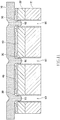
- the electrode material of the cathode electrode 50 enters the slit 60, since the upper portion of the slit 60 is filled with the protective member 80 formed of a part of the support member 70 as illustrated in FIG. 12 , the electrode material of the cathode electrode 50 by no means reaches the anode electrode 40.
- step S8 a plurality of the semiconductor devices 10 are completed.
- Each individual semiconductor device 10 is mounted in a package as needed.
- the package has a base plate made of copper (Cu) or the like, and the base plate and the cathode electrode 50 of the semiconductor device 10 are connected through a solder.
- the anode electrode 40 of the semiconductor device 10 is connected to a lead frame of the package through a bonding wire.
- dry etching is performed to form the plurality of slits 60 on the upper surface side of the gallium oxide substrate, and then the lower surface side of the gallium oxide substrate is ground and polished to singulate the substrate, thereby preventing the side surfaces 20c of the semiconductor layer 20 from being mechanically damaged.
- the substrate is singulated using a dicing blade or the like, cracking, chipping, cleavage and other defects do not occur in the side surfaces 20c.
- a (100) plane and a (001) plane have cleavability, so that in a case where the electrode forming surfaces 20a and 20b are (001) planes of ⁇ -Ga 2 O 3 , many horizontal cleavages may occur in the side surfaces 20c when the substrate is singulated using a dicing blade or the like.
- the side surfaces 20c are formed by dry etching, so that such cleavages hardly occur.
- gallium oxide powder is not scattered since the side surfaces 20c are covered with the insulating film 30. Further, gallium oxide has low heat conductivity, so that heat generated due to forward current is not efficiently radiated to easily cause element degradation.
- the thickness of the semiconductor layer 20 is reduced by polishing the back surface of the gallium oxide wafer W, so that heat radiation performance can be improved.
- the insulating film 30 is formed also on the inner wall 61 of the slit 60 simultaneously when the insulating film 30 is formed for the purpose of obtaining the field plate structure, so that it is possible to form the insulating film 30 both on the first electrode forming surface 20a and on the inner wall 61 of the slit 60 without involving an increase in the number of processes.
- the insulating film 30 (first part 31) formed on the first electrode forming surface 20a and the insulating film 30 (second part 32) formed on the side surfaces 20c are formed simultaneously, so that they are formed seamlessly. This makes it possible to effectively suppress a leak current flowing along the side surfaces 20c.
- the protective member 80 formed of a part of the flexible support member 70 is buried in the upper portion of the slit 60; however, when a support member 70 having high rigidity, i.e., having low flexibility is used, a protective member separated from the support member 70 may be buried in the slit 60 after formation of the slit 60 and before singulation of the gallium oxide substrate, as illustrated in FIG. 14 . Alternatively, the protective member 80 may be buried after singulation of the gallium oxide substrate and before formation of the cathode electrode 50.
- the electrode material of the cathode electrode 50 does not reach the anode electrode 40 even if it enters the slit 60.
- each slit 60 may be formed into a forward tapered shape as illustrated in FIG. 15 by adjusting dry etching conditions.
- the forward tapered shape refers to a shape in which the slit width is gradually reduced in the depth direction. This facilitates formation of the insulating film 30 on the inner wall 61 of the slit 60 in the formation process (step S3) of the insulating film 30.
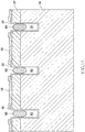
- the semiconductor device 10 When the slit 60 having such a forward tapered shape is formed, the semiconductor device 10 finally obtained has a tapered shape in which the XY cross section of the semiconductor layer 20 is increased from the first electrode forming surface 20a toward the second electrode forming surface 20b, as illustrated in FIG. 16 . This contributes to improvement in mounting stability on the package.
- the present invention is applied to a Schottky barrier diode in the above embodiment, the present invention is not limited to this and can be applied to other types of semiconductor devices provided that they are vertical semiconductor devices in which current flows in the thickness direction of the substrate.
- gallium oxide is used as the material of the semiconductor layer in the above embodiment, the present invention is not limited to this.
Landscapes
- Electrodes Of Semiconductors (AREA)
- Formation Of Insulating Films (AREA)
Abstract
Description
- The present invention relates to a semiconductor device and, more particularly, to a vertical semiconductor device in which current flows in the thickness direction of a substrate.
- Power semiconductor devices require significantly large currents to be supplied as compared to general semiconductor devices and, thus, often adopt a vertical structure in which current flows in the thickness direction of a substrate. For example, Patent Document 1 discloses a diode having the vertical structure. The diode described in Patent Document 1 has a structure in which a portion corresponding to a mesa groove is covered with a protective film.
- [Patent Document 1]
JP 2002-353227 A - However, in the diode described in Patent Document 1, a wafer side surface as a cutting surface is exposed, so that not only a leakage current easily occurs along the side surface, but also cracking, chipping, cleavage and other defects tend to occur in the side surface.
- It is therefore an object of the present invention to provide a vertical semiconductor device in which a leakage current flowing along the wafer side surface, and defects in the side surface, such as cracking, chipping and cleavage hardly occur.
- A semiconductor device according to the present invention includes a semiconductor layer including a first electrode forming surface, a second electrode forming surface positioned opposite to the first electrode forming surface, and a side surface having a first edge as a boundary with the first electrode forming surface and a second edge as a boundary with the second electrode forming surface; a first electrode formed on the first electrode forming surface; a second electrode formed on the second electrode forming surface; and an insulating film continuously formed from the first electrode forming surface to the side surface so as to cover the first edge.
- According to the present invention, the side surface of the semiconductor layer are covered with the insulating film, so that a leak current flowing along the side surface is reduced. Further, the side surface is protected by the insulating film, making cracking, chipping, cleavage, and the like less likely to occur. In addition, the insulating film is continuously formed from the first electrode forming surface to the side surface so as to cover the first edge, the first electrode forming surface and the side surface can be covered with the insulating film seamlessly.
- In the present invention, it is preferable that the semiconductor layer includes a semiconductor substrate constituting the second electrode forming surface and an epitaxial layer formed on the semiconductor substrate and constituting the first electrode forming surface, that at least a part of the first electrode comes into Schottky-contact with the epitaxial layer, and that the second electrode comes into ohmic contact with the semiconductor substrate. With this configuration, a Schottky barrier diode can be constituted.
- In this case, another part of the first electrode is preferably formed on the insulating film formed on the first electrode forming surface. With this configuration, a so-called field plate structure can be obtained.
- In the present invention, the semiconductor layer is preferably made of gallium oxide. With this configuration, a large band gap and a large breakdown electric field can be obtained, which is very advantageous in application to a switching element for power device.
- In the present invention, the semiconductor layer may have a tapered shape in which the cross section thereof is increased from the first electrode forming surface toward the second electrode forming surface. This facilitates the formation of the insulating film on the side surface.
- As described above, according to the present invention, there can be provided a vertical semiconductor device in which a leakage current flowing along the wafer side surface, and defects in the side surface, such as cracking, chipping and cleavage are reduced.
-
-
FIG. 1 is a cross-sectional view illustrating the configuration of asemiconductor device 10 according to an embodiment of the present invention. -
FIG. 2 is a top view of thesemiconductor device 10. -
FIG. 3 is a flowchart illustrating the manufacturing process of thesemiconductor device 10. -
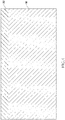
FIG. 4 is a cross-sectional view of thesemiconductor device 10 during the manufacturing process. -
FIG. 5 is a cross-sectional view of thesemiconductor device 10 during the manufacturing process. -
FIG. 6A is a plan view of thesemiconductor device 10 during the manufacturing process; andFIG. 6B is a schematic cross-sectional view taken along line B-B inFIG. 6A . -
FIG. 7 is a cross-sectional view of thesemiconductor device 10 during the manufacturing process. -
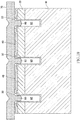
FIG. 8 is a cross-sectional view of thesemiconductor device 10 during the manufacturing process. -
FIG. 9 is a cross-sectional view of thesemiconductor device 10 during the manufacturing process. -
FIG. 10 is a cross-sectional view of thesemiconductor device 10 during the manufacturing process. -
FIG. 11 is a cross-sectional view of thesemiconductor device 10 during the manufacturing process. -
FIG. 12 is a cross-sectional view of thesemiconductor device 10 during the manufacturing process. -
FIG. 13 is a cross-sectional view of thesemiconductor device 10 during the manufacturing process. -
FIG. 14 is a cross-sectional view for explaining the manufacturing process of a modification of thesemiconductor device 10. -
FIG. 15 is a cross-sectional view for explaining the manufacturing process of a modification of thesemiconductor device 10. -
FIG. 16 is a cross-sectional view illustrating thesemiconductor device 10 in which a cross section is tapered. - Preferred embodiments of the present invention will be explained below in detail with reference to the accompanying drawings.
-
FIG. 1 is a cross-sectional view illustrating the configuration of asemiconductor device 10 according to an embodiment of the present invention.FIG. 2 is a top view of thesemiconductor device 10. The cross section illustrated inFIG. 1 corresponds to the cross section taken along line A-A inFIG. 2 . - The
semiconductor device 10 according to the present embodiment is a Schottky barrier diode and has asemiconductor layer 20 including asemiconductor substrate 21 and anepitaxial layer 22, both of which are made of gallium oxide (β-Ga2O3). In the present invention, thesemiconductor layer 20 will be referred to generically as "gallium oxide substrate" according to the situation. Silicon (Si) or tin (Sn) is introduced as an n-type dopant into thesemiconductor substrate 21 and theepitaxial layer 22. The concentration of the dopant is higher in thesemiconductor substrate 21 than in theepitaxial layer 22, whereby thesemiconductor substrate 21 and theepitaxial layer 22 function as an n+ layer and an n- layer, respectively. - The
semiconductor layer 20 has a firstelectrode forming surface 20a constituting the XY plane, a secondelectrode forming surface 20b positioned on the side opposite to the firstelectrode forming surface 20a and constituting the XY plane, and fourside surfaces 20c constituting the XZ or YZ plane. The first and secondelectrode forming surfaces electrode forming surface 20a is constituted by the upper surface of theepitaxial layer 22, and the secondelectrode forming surface 20b is constituted by the lower surface of thesemiconductor substrate 21. The boundary between the firstelectrode forming surface 20a and theside surfaces 20c constitutes a first edge E1, and the boundary between the secondelectrode forming surface 20b and theside surfaces 20c constitutes a second edge E2. - As illustrated in
FIGs. 1 and 2 , aninsulating film 30 made of SiO2, Si3N4, Al2O3, HfO2 or the like is formed on the firstelectrode forming surface 20a and theside surfaces 20c. Theinsulating film 30 includes afirst part 31 covering the firstelectrode forming surface 20a and asecond part 32 covering theside surfaces 20c and is continuously formed from the firstelectrode forming surface 20a to theside surfaces 20c so as to cover the first edge E1. Theinsulating film 30 is made of, e.g., silicon oxide (SiO2) and has a film thickness of about 300 nm. - The
first part 31 of theinsulating film 30 has an opening 30a exposing therethrough the firstelectrode forming surface 20a. Ananode electrode 40, which is a first electrode, is formed on the firstelectrode forming surface 20a through the opening 30a. With this configuration, theanode electrode 40 comes into Schottky-contact with theepitaxial layer 22. Theanode electrode 40 is formed of a laminated film of, e.g., platinum (Pt), titanium (Ti) and aluminum (Al). The film thicknesses of the platinum layer, titanium layer and aluminum layer are, e.g., about 50 nm, 5 nm and 1 µm, respectively. - The major part of the
anode electrode 40 comes into Schottky-contact with theepitaxial layer 22; the remaining part thereof covers thefirst part 31 of the insulatingfilm 30. As a result, a so-called field plate structure can be obtained. Generally, in the Schottky barrier diode, an electric field is concentrated on the end portion of the anode electrode, so that an element may be destroyed when the field strength at this portion exceeds its breakdown electric field strength. However, as in the present embodiment, when the end portion of theanode electrode 40 is formed on the insulatingfilm 30, current concentration on the end portion is alleviated to make it possible to improve reverse breakdown voltage. - On the other hand, a
cathode electrode 50, which is a second electrode, is formed on the secondelectrode forming surface 20b of thesemiconductor layer 20. Thecathode electrode 50 is formed of a laminated film of, e.g., titanium (Ti), nickel (Ni) and gold (Au) and comes into ohmic contact with thesemiconductor substrate 21. The film thicknesses of the titanium layer, nickel layer and gold layer are e.g., about 50 nm, 0.2 µm and 0.2 µm, respectively. - With the above configuration, the
semiconductor device 10 according to the present embodiment constitutes the Schottky barrier diode. The Schottky barrier diode is used in a switching element, wherein when a forward bias is applied between theanode electrode 40 and thecathode electrode 50, a Schottky barrier at the boundary between theanode electrode 40 and theepitaxial layer 22 decreases to cause current to flow from theanode electrode 40 to thecathode electrode 50. On the other hand, when a backward bias is applied between theanode electrode 40 and thecathode electrode 50, the Schottky barrier at the boundary between theanode electrode 40 and theepitaxial layer 22 is enhanced, with the result that current hardly flows. - In the
semiconductor device 10 according to the present embodiment, since the side surfaces 20c of thesemiconductor layer 20 are covered with the insulating film, a leak current flowing along the side surfaces 20c decreases, and cracking, chipping, cleavage and other defects in the side surfaces 20c hardly occur. Further, the insulatingfilm 30 is continuously formed from the firstelectrode forming surface 20a to the side surfaces 20c so as to cover the first edge E1, so that the effects described above are further enhanced as compared to a case where an insulating film covering the firstelectrode forming surface 20a and an insulating film covering the side surfaces 20c are separately formed. Further, cracking, chipping and other defects in the gallium oxide substrate at the first edge E1 are prevented. - The following describes a manufacturing method for the
semiconductor device 10 according to the present embodiment. -
FIG. 3 is a flowchart illustrating the manufacturing process of thesemiconductor device 10 according to the present embodiment. - As illustrated in
FIG. 4 , a gallium oxide wafer W obtained by slicing a bulk crystal grown by using a melt growth method is prepared, and theepitaxial layer 22 is formed on the surface of the gallium oxide wafer W. Theepitaxial layer 22 can be formed by epitaxially growing gallium oxide on the surface of the gallium oxide wafer W using a reactive sputtering method, a PLD method, an MBE method, an MOCVD method, an HVPE method, or the like. The carrier concentration and film thickness of theepitaxial layer 22 are adjusted so as to secure a designed breakdown voltage. As an example, in order to obtain a reverse breakdown voltage of about 600 V, the thickness and carrier concentration may be set to about 7 µm to 8 µm and 1 × 1016 cm-3. The carrier concentration is controlled by introducing a dopant functioning as an n-type carrier such as Si or Sn by a desired amount at the time of film formation. Thus, the gallium oxide substrate having theepitaxial layer 22 formed on the gallium oxide wafer W is completed (step S1). - Subsequently, as illustrated in
FIG. 5 , dry etching is performed with an element formation area of the firstelectrode forming surface 20a constituting the surface of theepitaxial layer 22 covered with an etching mask M1 to form a plurality ofslits 60 in the gallium oxide substrate (step S2). Theslits 60 are formed so as to penetrate theepitaxial layer 22 and to have a depth reaching the gallium oxide wafer W. Specifically, the depth of theslits 60 is made slightly larger than the final thickness of thesemiconductor layer 20. For example, when the final thickness of thesemiconductor layer 20 is 50 µm, the depth of theslits 60 is set to about 55 µm. - The
slits 60 can be formed by an RIE method using chlorine-based gas such as BCl3. Particularly, in order to reduce etching time, an ICP-RIE method enabling high-speed etching is preferably used. As the etching mask M1, a metal film such as nickel (Ni) that is not etched by chlorine-based gas is preferably used so as to increase selectivity with respect to, e.g., Ga2O3. In this case, the metal film serving as the etching mask M1 is formed to have a thickness of about 100 nm using an EB vapor deposition method or a sputtering method on the entire surface of theepitaxial layer 22 and is then patterned by photolithography. After that, dry etching is performed with the patterned etching mask M1 used as a mask to form the plurality ofslits 60 in the gallium oxide substrate. - As illustrated in
FIG. 6A as a plan view, the plurality of slits are formed so as to extend in the X- and Y-directions, and the rectangular areas surrounded by theslits 60 are each a part that finally becomes an element.FIG. 6B is a schematic cross-sectional view taken along line B-B inFIG. 6A . When, for example, the element size is 1 mm × 1 mm, theslits 60 each having a width of 20 µm are formed in the X- and Y-directions at 1.02 mm pitch. After the formation of theslits 60, the etching mask M M1 is removed using a general acid-based etching liquid, followed by substrate cleaning. - The thus formed
slits 60 have little damage in itsinner wall 61, unlike those formed by machining using a dicing blade or the like. Further, the flatness of theinner wall 61 is very high, specifically, irregularity thereof is 1 µm or less, and the surface property thereof is almost uniform. - Subsequently, as illustrated in
FIG. 7 , the insulatingfilm 30 made of SiO2, Si3N4, Al2O3, HfO2 or the like is formed on the surface of theepitaxial layer 22 and the inner walls of the respective slits 60 (step S3). The insulatingfilm 30 is preferably formed by a film formation method excellent in coverage, such as an ALD method or a CVD method, whereby not only the surface of theepitaxial layer 22, but also almost the entire surface of theinner wall 61 of each slit 60 is covered with the insulatingfilm 30. Also, each portion of first edge E1, the openings of therespective slits 60, are covered with the insulatingfilm 30. Further, a plurality of film formation methods may be combined for lamination of the insulatingfilm 30. - Subsequently, the
opening 30a is formed in the insulatingfilm 30 as illustrated inFIG. 8 , and then theanode electrode 40 is formed as illustrated inFIG. 9 (step S4). Theopening 30a is formed by patterning a resist by a normal photolithography method, and then by applying dry etching or wet etching to the insulatingfilm 30 with the resist used as a mask. However, the plurality ofslits 60 are formed in the gallium oxide substrate at this point, so that a film-type solid resist is more preferably used as the resist than a coating-type liquid resist. - The
anode electrode 40 can be formed by a vapor deposition method and patterned using a lift-off process. That is, a resist pattern having a planar size larger by about 5 µm than that of theopening 30a of the insulatingfilm 30 is formed, and then platinum (Pt), titanium (Ti) and aluminum (Al) are formed to have thicknesses of 50 nm, 5 nm and 1 µm, respectively, by vapor deposition. Then, the resist pattern is removed, whereby the metal layer formed on the resist pattern can be removed together with the rest pattern. In order to prevent the metal film from adhering to the inside of theslit 60, a film-type solid resist is preferably used. Alternatively, in place of patterning theanode electrode 40 formed on the entire surface, vapor deposition may be performed through a lattice-like metal mask to selectively form theanode electrode 40. However, in the present embodiment, theinner wall 61 of theslit 60 is covered with the insulatingfilm 30, so that even when a small amount of the metal material enters theslit 60, it does not contact the gallium oxide substrate. - Subsequently, as illustrated in
FIG. 10 , aflexible support member 70 is stuck onto the surface of the gallium oxide substrate (step S5). As theflexible support member 70, a member having high flexibility like a thick resin film is preferably used. By applying a certain pressure to the highlyflexible support member 70 on the surface of the gallium oxide substrate, thesupport member 70 is deformed and partly serves as aprotective member 80 buried in theslit 60. By theprotective member 80, theanode electrode 40 is spatially isolated from theslit 60. - Subsequently, as illustrated in
FIG. 11 , the back side, i.e., the lower surface of the gallium oxide wafer W is ground and polished with the gallium oxide substrate supported by the support member 70 (step S6). The grinding and polishing can be conducted in the same manner as for a general silicon substrate. The gallium oxide wafer W is ground and polished up to theslit 60, whereby the gallium oxide substrate including thesemiconductor substrate 21 andepitaxial layer 22 is singulated into a plurality of individual pieces . After the grinding and polishing, cleaning is performed to clean the polished surface. Although both the grinding and polishing are performed for singulation in the above description, the grinding may be omitted. - Subsequently, as illustrated in
FIG. 12 , thecathode electrode 50 is formed on the lower surface of thesemiconductor substrate 21 made of gallium oxide (step S7). Thecathode electrode 50 is preferably formed using a thin-film formation method with low coverage, such as a vapor deposition method or a sputtering method. As a result, thecathode electrode 50 is properly formed on the lower surface of thesemiconductor substrate 21, while an electrode material hardly gets into theinner wall 61 of theslit 60 to substantially prevent the electrode from being formed on theinner wall 61. Although a part of the electrode material of thecathode electrode 50 enters theslit 60, since the upper portion of theslit 60 is filled with theprotective member 80 formed of a part of thesupport member 70 as illustrated inFIG. 12 , the electrode material of thecathode electrode 50 by no means reaches theanode electrode 40. In order to prevent the electrode material from entering theslit 60, it is preferable to perform vapor deposition with theslit 60 covered with a lattice-shaped metal mask or the like to selectively form thecathode electrode 50 on the lower surface of thesemiconductor substrate 21. - Then, as illustrated in
FIG. 13 , thesupport member 70 is removed, whereby a plurality of thesemiconductor devices 10 are completed (step S8). Eachindividual semiconductor device 10 is mounted in a package as needed. The package has a base plate made of copper (Cu) or the like, and the base plate and thecathode electrode 50 of thesemiconductor device 10 are connected through a solder. Theanode electrode 40 of thesemiconductor device 10 is connected to a lead frame of the package through a bonding wire. - Thus, according to the manufacturing method for the
semiconductor device 10 of the present embodiment, dry etching is performed to form the plurality ofslits 60 on the upper surface side of the gallium oxide substrate, and then the lower surface side of the gallium oxide substrate is ground and polished to singulate the substrate, thereby preventing the side surfaces 20c of thesemiconductor layer 20 from being mechanically damaged. Thus, unlike a case where the substrate is singulated using a dicing blade or the like, cracking, chipping, cleavage and other defects do not occur in the side surfaces 20c. Particularly, in β-Ga2O3, a (100) plane and a (001) plane have cleavability, so that in a case where theelectrode forming surfaces semiconductor device 10 of the present embodiment, the side surfaces 20c are formed by dry etching, so that such cleavages hardly occur. Even if a small number of cleavages occur, the gallium oxide powder is not scattered since the side surfaces 20c are covered with the insulatingfilm 30. Further, gallium oxide has low heat conductivity, so that heat generated due to forward current is not efficiently radiated to easily cause element degradation. However, in the present embodiment, the thickness of thesemiconductor layer 20 is reduced by polishing the back surface of the gallium oxide wafer W, so that heat radiation performance can be improved. - In addition, the insulating
film 30 is formed also on theinner wall 61 of theslit 60 simultaneously when the insulatingfilm 30 is formed for the purpose of obtaining the field plate structure, so that it is possible to form the insulatingfilm 30 both on the firstelectrode forming surface 20a and on theinner wall 61 of theslit 60 without involving an increase in the number of processes. Thus, the insulating film 30 (first part 31) formed on the firstelectrode forming surface 20a and the insulating film 30 (second part 32) formed on the side surfaces 20c are formed simultaneously, so that they are formed seamlessly. This makes it possible to effectively suppress a leak current flowing along the side surfaces 20c. - In the above-described manufacturing method, the
protective member 80 formed of a part of theflexible support member 70 is buried in the upper portion of theslit 60; however, when asupport member 70 having high rigidity, i.e., having low flexibility is used, a protective member separated from thesupport member 70 may be buried in theslit 60 after formation of theslit 60 and before singulation of the gallium oxide substrate, as illustrated inFIG. 14 . Alternatively, theprotective member 80 may be buried after singulation of the gallium oxide substrate and before formation of thecathode electrode 50. At any rate, as far as theprotective member 80 is buried in theslit 60 at the time of formation of thecathode electrode 50, the electrode material of thecathode electrode 50 does not reach theanode electrode 40 even if it enters theslit 60. - Further, in the formation process (step S2) of the
slits 60, each slit 60 may be formed into a forward tapered shape as illustrated inFIG. 15 by adjusting dry etching conditions. The forward tapered shape refers to a shape in which the slit width is gradually reduced in the depth direction. This facilitates formation of the insulatingfilm 30 on theinner wall 61 of theslit 60 in the formation process (step S3) of the insulatingfilm 30. When theslit 60 having such a forward tapered shape is formed, thesemiconductor device 10 finally obtained has a tapered shape in which the XY cross section of thesemiconductor layer 20 is increased from the firstelectrode forming surface 20a toward the secondelectrode forming surface 20b, as illustrated inFIG. 16 . This contributes to improvement in mounting stability on the package. - While the preferred embodiments of the present invention have been described, the present invention is not limited to the above embodiments and may be implemented in various forms without departing from the sprit and the scope of the invention.
- For example, although the present invention is applied to a Schottky barrier diode in the above embodiment, the present invention is not limited to this and can be applied to other types of semiconductor devices provided that they are vertical semiconductor devices in which current flows in the thickness direction of the substrate.
- Further, although gallium oxide is used as the material of the semiconductor layer in the above embodiment, the present invention is not limited to this.
-
- 10
- semiconductor device
- 20
- semiconductor layer
- 20a
- first electrode forming surface
- 20b
- second electrode forming surface
- 20c
- side surface
- 21
- semiconductor substrate
- 22
- epitaxial layer
- 30
- insulating film
- 30a
- opening
- 31
- first part
- 32
- second part
- 40
- anode electrode
- 50
- cathode electrode
- 60
- slit
- 61
- inner wall
- 70
- support member
- 80
- protective member
- E1
- first edge
- E2
- second edge
- M1
- etching mask
- W
- gallium oxide wafer
Claims (5)
- A semiconductor device comprising:a semiconductor layer including a first electrode forming surface, a second electrode forming surface positioned opposite to the first electrode forming surface, and a side surface having a first edge as a boundary with the first electrode forming surface and a second edge as a boundary with the second electrode forming surface;a first electrode formed on the first electrode forming surface;a second electrode formed on the second electrode forming surface; andan insulating film continuously formed from the first electrode forming surface to the side surface so as to cover the first edge.
- The semiconductor device as claimed in claim 1,
wherein the semiconductor layer includes a semiconductor substrate constituting the second electrode forming surface and an epitaxial layer formed on the semiconductor substrate and constituting the first electrode forming surface, and
wherein at least a part of the first electrode comes into Schottky-contact with the epitaxial layer, and the second electrode comes into ohmic contact with the semiconductor substrate. - The semiconductor device as claimed in claim 2, wherein another part of the first electrode is formed on the insulating film formed on the first electrode forming surface.
- The semiconductor device as claimed in any one of claims 1 to 3, wherein the semiconductor layer is made of gallium oxide.
- The semiconductor device as claimed in any one of claims 1 to 4, wherein the semiconductor layer has a tapered shape in which a cross section thereof is increased from the first electrode forming surface toward the second electrode forming surface.
Applications Claiming Priority (2)
| Application Number | Priority Date | Filing Date | Title |
|---|---|---|---|
| JP2017064123A JP6809334B2 (en) | 2017-03-29 | 2017-03-29 | Semiconductor devices and their manufacturing methods |
| PCT/JP2018/002438 WO2018179768A1 (en) | 2017-03-29 | 2018-01-26 | Semiconductor device |
Publications (3)
| Publication Number | Publication Date |
|---|---|
| EP3608972A1 true EP3608972A1 (en) | 2020-02-12 |
| EP3608972A4 EP3608972A4 (en) | 2020-12-16 |
| EP3608972B1 EP3608972B1 (en) | 2024-03-20 |
Family
ID=63674938
Family Applications (1)
| Application Number | Title | Priority Date | Filing Date |
|---|---|---|---|
| EP18778040.8A Active EP3608972B1 (en) | 2017-03-29 | 2018-01-26 | Semiconductor device |
Country Status (5)
| Country | Link |
|---|---|
| US (1) | US11164953B2 (en) |
| EP (1) | EP3608972B1 (en) |
| JP (1) | JP6809334B2 (en) |
| CN (1) | CN110521004B (en) |
| WO (1) | WO2018179768A1 (en) |
Families Citing this family (7)
| Publication number | Priority date | Publication date | Assignee | Title |
|---|---|---|---|---|
| CN110809826B (en) * | 2017-06-29 | 2022-10-28 | 三菱电机株式会社 | Oxide semiconductor device and method for manufacturing oxide semiconductor device |
| JP7279354B2 (en) * | 2018-12-17 | 2023-05-23 | 富士電機株式会社 | Semiconductor device and method for identifying semiconductor device |
| JP7391326B2 (en) * | 2019-12-26 | 2023-12-05 | 株式会社ノベルクリスタルテクノロジー | semiconductor equipment |
| CN111540788A (en) * | 2020-06-18 | 2020-08-14 | 中国科学院半导体研究所 | Schottky diode and preparation method thereof |
| US12198998B2 (en) * | 2021-12-09 | 2025-01-14 | Nxp B.V. | Dielectric sidewall protection and sealing for semiconductor devices in a in wafer level packaging process |
| CN114497234B (en) * | 2022-01-25 | 2022-12-06 | 先之科半导体科技(东莞)有限公司 | Low-loss small-volume Schottky diode |
| WO2025182086A1 (en) * | 2024-03-01 | 2025-09-04 | 三菱電機株式会社 | Power semiconductor apparatus and power conversion apparatus |
Family Cites Families (10)
| Publication number | Priority date | Publication date | Assignee | Title |
|---|---|---|---|---|
| JPH09116133A (en) | 1995-10-13 | 1997-05-02 | Toyo Electric Mfg Co Ltd | High voltage semiconductor device |
| JP2002353227A (en) | 2001-05-28 | 2002-12-06 | Sanken Electric Co Ltd | Semiconductor device |
| JP2004119472A (en) * | 2002-09-24 | 2004-04-15 | Seiko Epson Corp | Semiconductor device and its manufacturing method, circuit board, and electronic equipment |
| JP4697397B2 (en) * | 2005-02-16 | 2011-06-08 | サンケン電気株式会社 | Composite semiconductor device |
| JP4945969B2 (en) * | 2005-09-07 | 2012-06-06 | 横河電機株式会社 | Semiconductor device and manufacturing method of semiconductor device |
| JP2009267032A (en) * | 2008-04-24 | 2009-11-12 | Toyota Motor Corp | Semiconductor device and manufacturing method thereof |
| JP2013102081A (en) * | 2011-11-09 | 2013-05-23 | Tamura Seisakusho Co Ltd | Schottky barrier diode |
| JP5914060B2 (en) * | 2012-03-09 | 2016-05-11 | 三菱電機株式会社 | Method for manufacturing silicon carbide semiconductor device |
| JP2014107499A (en) * | 2012-11-29 | 2014-06-09 | Sumitomo Electric Ind Ltd | Silicon carbide semiconductor device and method for manufacturing the same |
| JP2014225557A (en) * | 2013-05-16 | 2014-12-04 | 住友電気工業株式会社 | Method of manufacturing silicon carbide semiconductor device and semiconductor module, and silicon carbide semiconductor device and semiconductor module |
-
2017
- 2017-03-29 JP JP2017064123A patent/JP6809334B2/en active Active
-
2018
- 2018-01-26 US US16/496,715 patent/US11164953B2/en active Active
- 2018-01-26 CN CN201880022742.0A patent/CN110521004B/en active Active
- 2018-01-26 WO PCT/JP2018/002438 patent/WO2018179768A1/en not_active Ceased
- 2018-01-26 EP EP18778040.8A patent/EP3608972B1/en active Active
Also Published As
| Publication number | Publication date |
|---|---|
| CN110521004B (en) | 2023-01-10 |
| JP2018170305A (en) | 2018-11-01 |
| US11164953B2 (en) | 2021-11-02 |
| CN110521004A (en) | 2019-11-29 |
| EP3608972A4 (en) | 2020-12-16 |
| WO2018179768A1 (en) | 2018-10-04 |
| JP6809334B2 (en) | 2021-01-06 |
| EP3608972B1 (en) | 2024-03-20 |
| US20200111882A1 (en) | 2020-04-09 |
Similar Documents
| Publication | Publication Date | Title |
|---|---|---|
| US11164953B2 (en) | Semiconductor device | |
| TWI798402B (en) | Schottky barrier diode | |
| EP3703137A1 (en) | Schottky barrier diode | |
| KR102571505B1 (en) | semiconductor device | |
| US20210343879A1 (en) | Schottky barrier diode | |
| US12396188B2 (en) | Schottky barrier diode | |
| CN108788473B (en) | Compound semiconductor device, method for manufacturing the same, and resin-sealed semiconductor device | |
| US12563757B2 (en) | Schottky barrier diode | |
| US9257574B2 (en) | Diode and method of manufacturing diode | |
| WO2023095396A1 (en) | Junction barrier schottky diode | |
| EP3683847A1 (en) | Schottky barrier diode | |
| JP6794896B2 (en) | Manufacturing method of gallium oxide semiconductor device | |
| US20260006809A1 (en) | Junction barrier schottky diode | |
| EP4084043A1 (en) | Semiconductor element, method for manufacturing semiconductor element, semiconductor device, and method for manufacturing semiconductor device | |
| JP7843603B2 (en) | Schottky barrier diode | |
| US12520510B2 (en) | Schottky barrier diode | |
| US20240072179A1 (en) | Schottky barrier diode | |
| US12635520B2 (en) | Semiconductor element, method for manufacturing semiconductor element, semiconductor device, and method for manufacturing semiconductor device | |
| US20260013157A1 (en) | Schottky barrier diode |
Legal Events
| Date | Code | Title | Description |
|---|---|---|---|
| STAA | Information on the status of an ep patent application or granted ep patent |
Free format text: STATUS: THE INTERNATIONAL PUBLICATION HAS BEEN MADE |
|
| PUAI | Public reference made under article 153(3) epc to a published international application that has entered the european phase |
Free format text: ORIGINAL CODE: 0009012 |
|
| STAA | Information on the status of an ep patent application or granted ep patent |
Free format text: STATUS: REQUEST FOR EXAMINATION WAS MADE |
|
| 17P | Request for examination filed |
Effective date: 20191024 |
|
| AK | Designated contracting states |
Kind code of ref document: A1 Designated state(s): AL AT BE BG CH CY CZ DE DK EE ES FI FR GB GR HR HU IE IS IT LI LT LU LV MC MK MT NL NO PL PT RO RS SE SI SK SM TR |
|
| AX | Request for extension of the european patent |
Extension state: BA ME |
|
| DAV | Request for validation of the european patent (deleted) | ||
| DAX | Request for extension of the european patent (deleted) | ||
| A4 | Supplementary search report drawn up and despatched |
Effective date: 20201116 |
|
| RIC1 | Information provided on ipc code assigned before grant |
Ipc: H01L 23/31 20060101ALI20201110BHEP Ipc: H01L 29/24 20060101ALI20201110BHEP Ipc: H01L 29/47 20060101ALN20201110BHEP Ipc: H01L 21/78 20060101ALI20201110BHEP Ipc: H01L 21/365 20060101ALI20201110BHEP Ipc: H01L 21/316 20060101ALI20201110BHEP Ipc: H01L 29/872 20060101AFI20201110BHEP Ipc: H01L 29/06 20060101ALI20201110BHEP Ipc: H01L 21/318 20060101ALI20201110BHEP |
|
| STAA | Information on the status of an ep patent application or granted ep patent |
Free format text: STATUS: EXAMINATION IS IN PROGRESS |
|
| 17Q | First examination report despatched |
Effective date: 20220208 |
|
| RIC1 | Information provided on ipc code assigned before grant |
Ipc: H01L 29/47 20060101ALN20230913BHEP Ipc: H01L 21/78 20060101ALI20230913BHEP Ipc: H01L 29/06 20060101ALI20230913BHEP Ipc: H01L 21/365 20060101ALI20230913BHEP Ipc: H01L 21/318 20060101ALI20230913BHEP Ipc: H01L 21/316 20060101ALI20230913BHEP Ipc: H01L 23/31 20060101ALI20230913BHEP Ipc: H01L 29/24 20060101ALI20230913BHEP Ipc: H01L 29/872 20060101AFI20230913BHEP |
|
| RIC1 | Information provided on ipc code assigned before grant |
Ipc: H01L 29/47 20060101ALN20230915BHEP Ipc: H01L 21/78 20060101ALI20230915BHEP Ipc: H01L 29/06 20060101ALI20230915BHEP Ipc: H01L 21/365 20060101ALI20230915BHEP Ipc: H01L 21/318 20060101ALI20230915BHEP Ipc: H01L 21/316 20060101ALI20230915BHEP Ipc: H01L 23/31 20060101ALI20230915BHEP Ipc: H01L 29/24 20060101ALI20230915BHEP Ipc: H01L 29/872 20060101AFI20230915BHEP |
|
| GRAP | Despatch of communication of intention to grant a patent |
Free format text: ORIGINAL CODE: EPIDOSNIGR1 |
|
| STAA | Information on the status of an ep patent application or granted ep patent |
Free format text: STATUS: GRANT OF PATENT IS INTENDED |
|
| RIC1 | Information provided on ipc code assigned before grant |
Ipc: H01L 29/47 20060101ALN20231012BHEP Ipc: H01L 21/78 20060101ALI20231012BHEP Ipc: H01L 29/06 20060101ALI20231012BHEP Ipc: H01L 21/365 20060101ALI20231012BHEP Ipc: H01L 21/318 20060101ALI20231012BHEP Ipc: H01L 21/316 20060101ALI20231012BHEP Ipc: H01L 23/31 20060101ALI20231012BHEP Ipc: H01L 29/24 20060101ALI20231012BHEP Ipc: H01L 29/872 20060101AFI20231012BHEP |
|
| RIC1 | Information provided on ipc code assigned before grant |
Ipc: H01L 29/47 20060101ALN20231019BHEP Ipc: H01L 21/78 20060101ALI20231019BHEP Ipc: H01L 29/06 20060101ALI20231019BHEP Ipc: H01L 21/365 20060101ALI20231019BHEP Ipc: H01L 21/318 20060101ALI20231019BHEP Ipc: H01L 21/316 20060101ALI20231019BHEP Ipc: H01L 23/31 20060101ALI20231019BHEP Ipc: H01L 29/24 20060101ALI20231019BHEP Ipc: H01L 29/872 20060101AFI20231019BHEP |
|
| INTG | Intention to grant announced |
Effective date: 20231031 |
|
| GRAS | Grant fee paid |
Free format text: ORIGINAL CODE: EPIDOSNIGR3 |
|
| GRAA | (expected) grant |
Free format text: ORIGINAL CODE: 0009210 |
|
| STAA | Information on the status of an ep patent application or granted ep patent |
Free format text: STATUS: THE PATENT HAS BEEN GRANTED |
|
| AK | Designated contracting states |
Kind code of ref document: B1 Designated state(s): AL AT BE BG CH CY CZ DE DK EE ES FI FR GB GR HR HU IE IS IT LI LT LU LV MC MK MT NL NO PL PT RO RS SE SI SK SM TR |
|
| REG | Reference to a national code |
Ref country code: GB Ref legal event code: FG4D |
|
| REG | Reference to a national code |
Ref country code: CH Ref legal event code: EP |
|
| REG | Reference to a national code |
Ref country code: IE Ref legal event code: FG4D |
|
| REG | Reference to a national code |
Ref country code: DE Ref legal event code: R096 Ref document number: 602018066885 Country of ref document: DE |
|
| PG25 | Lapsed in a contracting state [announced via postgrant information from national office to epo] |
Ref country code: LT Free format text: LAPSE BECAUSE OF FAILURE TO SUBMIT A TRANSLATION OF THE DESCRIPTION OR TO PAY THE FEE WITHIN THE PRESCRIBED TIME-LIMIT Effective date: 20240320 |
|
| REG | Reference to a national code |
Ref country code: LT Ref legal event code: MG9D |
|
| PG25 | Lapsed in a contracting state [announced via postgrant information from national office to epo] |
Ref country code: GR Free format text: LAPSE BECAUSE OF FAILURE TO SUBMIT A TRANSLATION OF THE DESCRIPTION OR TO PAY THE FEE WITHIN THE PRESCRIBED TIME-LIMIT Effective date: 20240621 |
|
| PG25 | Lapsed in a contracting state [announced via postgrant information from national office to epo] |
Ref country code: HR Free format text: LAPSE BECAUSE OF FAILURE TO SUBMIT A TRANSLATION OF THE DESCRIPTION OR TO PAY THE FEE WITHIN THE PRESCRIBED TIME-LIMIT Effective date: 20240320 Ref country code: RS Free format text: LAPSE BECAUSE OF FAILURE TO SUBMIT A TRANSLATION OF THE DESCRIPTION OR TO PAY THE FEE WITHIN THE PRESCRIBED TIME-LIMIT Effective date: 20240620 |
|
| REG | Reference to a national code |
Ref country code: NL Ref legal event code: MP Effective date: 20240320 |
|
| PG25 | Lapsed in a contracting state [announced via postgrant information from national office to epo] |
Ref country code: RS Free format text: LAPSE BECAUSE OF FAILURE TO SUBMIT A TRANSLATION OF THE DESCRIPTION OR TO PAY THE FEE WITHIN THE PRESCRIBED TIME-LIMIT Effective date: 20240620 Ref country code: NO Free format text: LAPSE BECAUSE OF FAILURE TO SUBMIT A TRANSLATION OF THE DESCRIPTION OR TO PAY THE FEE WITHIN THE PRESCRIBED TIME-LIMIT Effective date: 20240620 Ref country code: LT Free format text: LAPSE BECAUSE OF FAILURE TO SUBMIT A TRANSLATION OF THE DESCRIPTION OR TO PAY THE FEE WITHIN THE PRESCRIBED TIME-LIMIT Effective date: 20240320 Ref country code: HR Free format text: LAPSE BECAUSE OF FAILURE TO SUBMIT A TRANSLATION OF THE DESCRIPTION OR TO PAY THE FEE WITHIN THE PRESCRIBED TIME-LIMIT Effective date: 20240320 Ref country code: GR Free format text: LAPSE BECAUSE OF FAILURE TO SUBMIT A TRANSLATION OF THE DESCRIPTION OR TO PAY THE FEE WITHIN THE PRESCRIBED TIME-LIMIT Effective date: 20240621 Ref country code: FI Free format text: LAPSE BECAUSE OF FAILURE TO SUBMIT A TRANSLATION OF THE DESCRIPTION OR TO PAY THE FEE WITHIN THE PRESCRIBED TIME-LIMIT Effective date: 20240320 Ref country code: BG Free format text: LAPSE BECAUSE OF FAILURE TO SUBMIT A TRANSLATION OF THE DESCRIPTION OR TO PAY THE FEE WITHIN THE PRESCRIBED TIME-LIMIT Effective date: 20240320 |
|
| REG | Reference to a national code |
Ref country code: AT Ref legal event code: MK05 Ref document number: 1668616 Country of ref document: AT Kind code of ref document: T Effective date: 20240320 |
|
| PG25 | Lapsed in a contracting state [announced via postgrant information from national office to epo] |
Ref country code: SE Free format text: LAPSE BECAUSE OF FAILURE TO SUBMIT A TRANSLATION OF THE DESCRIPTION OR TO PAY THE FEE WITHIN THE PRESCRIBED TIME-LIMIT Effective date: 20240320 Ref country code: LV Free format text: LAPSE BECAUSE OF FAILURE TO SUBMIT A TRANSLATION OF THE DESCRIPTION OR TO PAY THE FEE WITHIN THE PRESCRIBED TIME-LIMIT Effective date: 20240320 |
|
| PG25 | Lapsed in a contracting state [announced via postgrant information from national office to epo] |
Ref country code: NL Free format text: LAPSE BECAUSE OF FAILURE TO SUBMIT A TRANSLATION OF THE DESCRIPTION OR TO PAY THE FEE WITHIN THE PRESCRIBED TIME-LIMIT Effective date: 20240320 |
|
| PG25 | Lapsed in a contracting state [announced via postgrant information from national office to epo] |
Ref country code: NL Free format text: LAPSE BECAUSE OF FAILURE TO SUBMIT A TRANSLATION OF THE DESCRIPTION OR TO PAY THE FEE WITHIN THE PRESCRIBED TIME-LIMIT Effective date: 20240320 |
|
| PG25 | Lapsed in a contracting state [announced via postgrant information from national office to epo] |
Ref country code: IS Free format text: LAPSE BECAUSE OF FAILURE TO SUBMIT A TRANSLATION OF THE DESCRIPTION OR TO PAY THE FEE WITHIN THE PRESCRIBED TIME-LIMIT Effective date: 20240720 |
|
| PG25 | Lapsed in a contracting state [announced via postgrant information from national office to epo] |
Ref country code: PT Free format text: LAPSE BECAUSE OF FAILURE TO SUBMIT A TRANSLATION OF THE DESCRIPTION OR TO PAY THE FEE WITHIN THE PRESCRIBED TIME-LIMIT Effective date: 20240722 Ref country code: SM Free format text: LAPSE BECAUSE OF FAILURE TO SUBMIT A TRANSLATION OF THE DESCRIPTION OR TO PAY THE FEE WITHIN THE PRESCRIBED TIME-LIMIT Effective date: 20240320 |
|
| PG25 | Lapsed in a contracting state [announced via postgrant information from national office to epo] |
Ref country code: ES Free format text: LAPSE BECAUSE OF FAILURE TO SUBMIT A TRANSLATION OF THE DESCRIPTION OR TO PAY THE FEE WITHIN THE PRESCRIBED TIME-LIMIT Effective date: 20240320 |
|
| PG25 | Lapsed in a contracting state [announced via postgrant information from national office to epo] |
Ref country code: EE Free format text: LAPSE BECAUSE OF FAILURE TO SUBMIT A TRANSLATION OF THE DESCRIPTION OR TO PAY THE FEE WITHIN THE PRESCRIBED TIME-LIMIT Effective date: 20240320 Ref country code: CZ Free format text: LAPSE BECAUSE OF FAILURE TO SUBMIT A TRANSLATION OF THE DESCRIPTION OR TO PAY THE FEE WITHIN THE PRESCRIBED TIME-LIMIT Effective date: 20240320 |
|
| PG25 | Lapsed in a contracting state [announced via postgrant information from national office to epo] |
Ref country code: AT Free format text: LAPSE BECAUSE OF FAILURE TO SUBMIT A TRANSLATION OF THE DESCRIPTION OR TO PAY THE FEE WITHIN THE PRESCRIBED TIME-LIMIT Effective date: 20240320 |
|
| PG25 | Lapsed in a contracting state [announced via postgrant information from national office to epo] |
Ref country code: PL Free format text: LAPSE BECAUSE OF FAILURE TO SUBMIT A TRANSLATION OF THE DESCRIPTION OR TO PAY THE FEE WITHIN THE PRESCRIBED TIME-LIMIT Effective date: 20240320 |
|
| PG25 | Lapsed in a contracting state [announced via postgrant information from national office to epo] |
Ref country code: SK Free format text: LAPSE BECAUSE OF FAILURE TO SUBMIT A TRANSLATION OF THE DESCRIPTION OR TO PAY THE FEE WITHIN THE PRESCRIBED TIME-LIMIT Effective date: 20240320 |
|
| PG25 | Lapsed in a contracting state [announced via postgrant information from national office to epo] |
Ref country code: SM Free format text: LAPSE BECAUSE OF FAILURE TO SUBMIT A TRANSLATION OF THE DESCRIPTION OR TO PAY THE FEE WITHIN THE PRESCRIBED TIME-LIMIT Effective date: 20240320 Ref country code: SK Free format text: LAPSE BECAUSE OF FAILURE TO SUBMIT A TRANSLATION OF THE DESCRIPTION OR TO PAY THE FEE WITHIN THE PRESCRIBED TIME-LIMIT Effective date: 20240320 Ref country code: RO Free format text: LAPSE BECAUSE OF FAILURE TO SUBMIT A TRANSLATION OF THE DESCRIPTION OR TO PAY THE FEE WITHIN THE PRESCRIBED TIME-LIMIT Effective date: 20240320 Ref country code: PT Free format text: LAPSE BECAUSE OF FAILURE TO SUBMIT A TRANSLATION OF THE DESCRIPTION OR TO PAY THE FEE WITHIN THE PRESCRIBED TIME-LIMIT Effective date: 20240722 Ref country code: PL Free format text: LAPSE BECAUSE OF FAILURE TO SUBMIT A TRANSLATION OF THE DESCRIPTION OR TO PAY THE FEE WITHIN THE PRESCRIBED TIME-LIMIT Effective date: 20240320 Ref country code: IS Free format text: LAPSE BECAUSE OF FAILURE TO SUBMIT A TRANSLATION OF THE DESCRIPTION OR TO PAY THE FEE WITHIN THE PRESCRIBED TIME-LIMIT Effective date: 20240720 Ref country code: ES Free format text: LAPSE BECAUSE OF FAILURE TO SUBMIT A TRANSLATION OF THE DESCRIPTION OR TO PAY THE FEE WITHIN THE PRESCRIBED TIME-LIMIT Effective date: 20240320 Ref country code: EE Free format text: LAPSE BECAUSE OF FAILURE TO SUBMIT A TRANSLATION OF THE DESCRIPTION OR TO PAY THE FEE WITHIN THE PRESCRIBED TIME-LIMIT Effective date: 20240320 Ref country code: CZ Free format text: LAPSE BECAUSE OF FAILURE TO SUBMIT A TRANSLATION OF THE DESCRIPTION OR TO PAY THE FEE WITHIN THE PRESCRIBED TIME-LIMIT Effective date: 20240320 Ref country code: AT Free format text: LAPSE BECAUSE OF FAILURE TO SUBMIT A TRANSLATION OF THE DESCRIPTION OR TO PAY THE FEE WITHIN THE PRESCRIBED TIME-LIMIT Effective date: 20240320 |
|
| REG | Reference to a national code |
Ref country code: DE Ref legal event code: R079 Ref document number: 602018066885 Country of ref document: DE Free format text: PREVIOUS MAIN CLASS: H01L0029872000 Ipc: H10D0008600000 |
|
| PG25 | Lapsed in a contracting state [announced via postgrant information from national office to epo] |
Ref country code: IT Free format text: LAPSE BECAUSE OF FAILURE TO SUBMIT A TRANSLATION OF THE DESCRIPTION OR TO PAY THE FEE WITHIN THE PRESCRIBED TIME-LIMIT Effective date: 20240320 |
|
| REG | Reference to a national code |
Ref country code: DE Ref legal event code: R097 Ref document number: 602018066885 Country of ref document: DE |
|
| PG25 | Lapsed in a contracting state [announced via postgrant information from national office to epo] |
Ref country code: IT Free format text: LAPSE BECAUSE OF FAILURE TO SUBMIT A TRANSLATION OF THE DESCRIPTION OR TO PAY THE FEE WITHIN THE PRESCRIBED TIME-LIMIT Effective date: 20240320 |
|
| PG25 | Lapsed in a contracting state [announced via postgrant information from national office to epo] |
Ref country code: DK Free format text: LAPSE BECAUSE OF FAILURE TO SUBMIT A TRANSLATION OF THE DESCRIPTION OR TO PAY THE FEE WITHIN THE PRESCRIBED TIME-LIMIT Effective date: 20240320 |
|
| PLBE | No opposition filed within time limit |
Free format text: ORIGINAL CODE: 0009261 |
|
| STAA | Information on the status of an ep patent application or granted ep patent |
Free format text: STATUS: NO OPPOSITION FILED WITHIN TIME LIMIT |
|
| PG25 | Lapsed in a contracting state [announced via postgrant information from national office to epo] |
Ref country code: DK Free format text: LAPSE BECAUSE OF FAILURE TO SUBMIT A TRANSLATION OF THE DESCRIPTION OR TO PAY THE FEE WITHIN THE PRESCRIBED TIME-LIMIT Effective date: 20240320 |
|
| 26N | No opposition filed |
Effective date: 20241223 |
|
| PG25 | Lapsed in a contracting state [announced via postgrant information from national office to epo] |
Ref country code: SI Free format text: LAPSE BECAUSE OF FAILURE TO SUBMIT A TRANSLATION OF THE DESCRIPTION OR TO PAY THE FEE WITHIN THE PRESCRIBED TIME-LIMIT Effective date: 20240320 |
|
| REG | Reference to a national code |
Ref country code: CH Ref legal event code: PL |
|
| PG25 | Lapsed in a contracting state [announced via postgrant information from national office to epo] |
Ref country code: MC Free format text: LAPSE BECAUSE OF FAILURE TO SUBMIT A TRANSLATION OF THE DESCRIPTION OR TO PAY THE FEE WITHIN THE PRESCRIBED TIME-LIMIT Effective date: 20240320 Ref country code: LU Free format text: LAPSE BECAUSE OF NON-PAYMENT OF DUE FEES Effective date: 20250126 |
|
| GBPC | Gb: european patent ceased through non-payment of renewal fee |
Effective date: 20250126 |
|
| PG25 | Lapsed in a contracting state [announced via postgrant information from national office to epo] |
Ref country code: GB Free format text: LAPSE BECAUSE OF NON-PAYMENT OF DUE FEES Effective date: 20250126 Ref country code: BE Free format text: LAPSE BECAUSE OF NON-PAYMENT OF DUE FEES Effective date: 20250131 |
|
| PG25 | Lapsed in a contracting state [announced via postgrant information from national office to epo] |
Ref country code: FR Free format text: LAPSE BECAUSE OF NON-PAYMENT OF DUE FEES Effective date: 20250131 |
|
| PG25 | Lapsed in a contracting state [announced via postgrant information from national office to epo] |
Ref country code: CH Free format text: LAPSE BECAUSE OF NON-PAYMENT OF DUE FEES Effective date: 20250131 |
|
| REG | Reference to a national code |
Ref country code: BE Ref legal event code: MM Effective date: 20250131 |
|
| PG25 | Lapsed in a contracting state [announced via postgrant information from national office to epo] |
Ref country code: IE Free format text: LAPSE BECAUSE OF NON-PAYMENT OF DUE FEES Effective date: 20250126 |
|
| PGFP | Annual fee paid to national office [announced via postgrant information from national office to epo] |
Ref country code: DE Payment date: 20251203 Year of fee payment: 9 |