EP3608709A1 - Multi-colored pixelated display with a diffractive element - Google Patents
Multi-colored pixelated display with a diffractive element Download PDFInfo
- Publication number
- EP3608709A1 EP3608709A1 EP19200745.8A EP19200745A EP3608709A1 EP 3608709 A1 EP3608709 A1 EP 3608709A1 EP 19200745 A EP19200745 A EP 19200745A EP 3608709 A1 EP3608709 A1 EP 3608709A1
- Authority
- EP
- European Patent Office
- Prior art keywords
- display
- approximately
- pixels
- diffraction
- sparkle reduction
- Prior art date
- Legal status (The legal status is an assumption and is not a legal conclusion. Google has not performed a legal analysis and makes no representation as to the accuracy of the status listed.)
- Granted
Links
Images

Classifications
-
- G—PHYSICS
- G02—OPTICS
- G02F—OPTICAL DEVICES OR ARRANGEMENTS FOR THE CONTROL OF LIGHT BY MODIFICATION OF THE OPTICAL PROPERTIES OF THE MEDIA OF THE ELEMENTS INVOLVED THEREIN; NON-LINEAR OPTICS; FREQUENCY-CHANGING OF LIGHT; OPTICAL LOGIC ELEMENTS; OPTICAL ANALOGUE/DIGITAL CONVERTERS
- G02F1/00—Devices or arrangements for the control of the intensity, colour, phase, polarisation or direction of light arriving from an independent light source, e.g. switching, gating or modulating; Non-linear optics
- G02F1/01—Devices or arrangements for the control of the intensity, colour, phase, polarisation or direction of light arriving from an independent light source, e.g. switching, gating or modulating; Non-linear optics for the control of the intensity, phase, polarisation or colour
- G02F1/13—Devices or arrangements for the control of the intensity, colour, phase, polarisation or direction of light arriving from an independent light source, e.g. switching, gating or modulating; Non-linear optics for the control of the intensity, phase, polarisation or colour based on liquid crystals, e.g. single liquid crystal display cells
- G02F1/133—Constructional arrangements; Operation of liquid crystal cells; Circuit arrangements
- G02F1/1333—Constructional arrangements; Manufacturing methods
- G02F1/1335—Structural association of cells with optical devices, e.g. polarisers or reflectors
- G02F1/133504—Diffusing, scattering, diffracting elements
-
- G—PHYSICS
- G02—OPTICS
- G02B—OPTICAL ELEMENTS, SYSTEMS OR APPARATUS
- G02B5/00—Optical elements other than lenses
- G02B5/02—Diffusing elements; Afocal elements
- G02B5/0205—Diffusing elements; Afocal elements characterised by the diffusing properties
- G02B5/021—Diffusing elements; Afocal elements characterised by the diffusing properties the diffusion taking place at the element's surface, e.g. by means of surface roughening or microprismatic structures
- G02B5/0215—Diffusing elements; Afocal elements characterised by the diffusing properties the diffusion taking place at the element's surface, e.g. by means of surface roughening or microprismatic structures the surface having a regular structure
-
- G—PHYSICS
- G02—OPTICS
- G02B—OPTICAL ELEMENTS, SYSTEMS OR APPARATUS
- G02B5/00—Optical elements other than lenses
- G02B5/18—Diffraction gratings
- G02B5/1842—Gratings for image generation
-
- G—PHYSICS
- G02—OPTICS
- G02F—OPTICAL DEVICES OR ARRANGEMENTS FOR THE CONTROL OF LIGHT BY MODIFICATION OF THE OPTICAL PROPERTIES OF THE MEDIA OF THE ELEMENTS INVOLVED THEREIN; NON-LINEAR OPTICS; FREQUENCY-CHANGING OF LIGHT; OPTICAL LOGIC ELEMENTS; OPTICAL ANALOGUE/DIGITAL CONVERTERS
- G02F1/00—Devices or arrangements for the control of the intensity, colour, phase, polarisation or direction of light arriving from an independent light source, e.g. switching, gating or modulating; Non-linear optics
- G02F1/01—Devices or arrangements for the control of the intensity, colour, phase, polarisation or direction of light arriving from an independent light source, e.g. switching, gating or modulating; Non-linear optics for the control of the intensity, phase, polarisation or colour
- G02F1/13—Devices or arrangements for the control of the intensity, colour, phase, polarisation or direction of light arriving from an independent light source, e.g. switching, gating or modulating; Non-linear optics for the control of the intensity, phase, polarisation or colour based on liquid crystals, e.g. single liquid crystal display cells
- G02F1/133—Constructional arrangements; Operation of liquid crystal cells; Circuit arrangements
- G02F1/1333—Constructional arrangements; Manufacturing methods
- G02F1/1335—Structural association of cells with optical devices, e.g. polarisers or reflectors
- G02F1/133502—Antiglare, refractive index matching layers
-
- G—PHYSICS
- G02—OPTICS
- G02F—OPTICAL DEVICES OR ARRANGEMENTS FOR THE CONTROL OF LIGHT BY MODIFICATION OF THE OPTICAL PROPERTIES OF THE MEDIA OF THE ELEMENTS INVOLVED THEREIN; NON-LINEAR OPTICS; FREQUENCY-CHANGING OF LIGHT; OPTICAL LOGIC ELEMENTS; OPTICAL ANALOGUE/DIGITAL CONVERTERS
- G02F1/00—Devices or arrangements for the control of the intensity, colour, phase, polarisation or direction of light arriving from an independent light source, e.g. switching, gating or modulating; Non-linear optics
- G02F1/01—Devices or arrangements for the control of the intensity, colour, phase, polarisation or direction of light arriving from an independent light source, e.g. switching, gating or modulating; Non-linear optics for the control of the intensity, phase, polarisation or colour
- G02F1/13—Devices or arrangements for the control of the intensity, colour, phase, polarisation or direction of light arriving from an independent light source, e.g. switching, gating or modulating; Non-linear optics for the control of the intensity, phase, polarisation or colour based on liquid crystals, e.g. single liquid crystal display cells
- G02F1/133—Constructional arrangements; Operation of liquid crystal cells; Circuit arrangements
- G02F1/1333—Constructional arrangements; Manufacturing methods
- G02F1/1335—Structural association of cells with optical devices, e.g. polarisers or reflectors
- G02F1/13356—Structural association of cells with optical devices, e.g. polarisers or reflectors characterised by the placement of the optical elements
- G02F1/133562—Structural association of cells with optical devices, e.g. polarisers or reflectors characterised by the placement of the optical elements on the viewer side
-
- G—PHYSICS
- G02—OPTICS
- G02F—OPTICAL DEVICES OR ARRANGEMENTS FOR THE CONTROL OF LIGHT BY MODIFICATION OF THE OPTICAL PROPERTIES OF THE MEDIA OF THE ELEMENTS INVOLVED THEREIN; NON-LINEAR OPTICS; FREQUENCY-CHANGING OF LIGHT; OPTICAL LOGIC ELEMENTS; OPTICAL ANALOGUE/DIGITAL CONVERTERS
- G02F2201/00—Constructional arrangements not provided for in groups G02F1/00 - G02F7/00
- G02F2201/30—Constructional arrangements not provided for in groups G02F1/00 - G02F7/00 grating
- G02F2201/305—Constructional arrangements not provided for in groups G02F1/00 - G02F7/00 grating diffraction grating
Definitions
- the present disclosure relates to pixelated displays and, more particularly, to sparkle reduction technology for use in pixelated displays.
- Pixelated displays such as liquid crystal displays (LCDs) and organic light emitting diodes (OLEDs) are widely used in a variety of information, communication, and entertainment devices.
- Display “sparkle” is a generally undesirable side effect that can occur when the display surface is scratched, soiled, or otherwise marked and typically manifests itself as bright, dark, and/or colored grains or spots, at approximately the pixel-level size scale, the pattern of which typically appears to shift with changing viewing angle.
- multi-colored pixelated displays are provided where a sparkle reduction surface comprising a micron grade diffraction element is positioned between the image display element and the display surface.
- a multi-colored pixelated display comprising an image display element and a transparent display cover.
- the image display element comprises an array of display pixels divided into a plurality of display sub-pixels associated with respective dedicated display color components.
- the transparent display cover comprises a display surface that is susceptible to marking and a sparkle reduction surface.
- the sparkle reduction surface is positioned between the image display element and the display surface along an optical path of the pixelated display and is spaced from the image display element by an optical distance D.
- the sparkle reduction surface comprises a micron grade diffraction element.
- the image display element comprises an array of display pixels arranged at a pixel pitch x and divided into a plurality of display sub-pixels associated with respective dedicated display color components.
- the display sub-pixels of an individual display pixel are associated with a dedicated display color component, one of which lies at a wavelength ⁇ G between approximately 490 nm and approximately 570 nm.
- a multi-colored pixelated display 10 according to one embodiment of the present disclosure is illustrated in Fig. 1 and comprises an image display element 20 and a transparent display cover 30 spaced from the image display element 20.
- the image display element 20 comprises an array of display pixels that are each divided into a plurality of display sub-pixels associated with respective dedicated display color components.
- Fig. 3 shows an embodiment where an array of display pixels are each divided along the X direction into three sub-pixels, one each for the red (R), green (G), and blue (B) color components of the display.
- RGB red
- G green
- B blue
- color images are generally created by using adjacent red (R), green (G), and blue (B) sub-pixels. These sub-pixels are approximately one third of the size (or pitch) of the pixel in the X direction and are equal to the size of the pixel in the Y direction.
- pixel and sub-pixel geometries other than that shown in Fig. 3 .
- Other pixel geometries include, but are not limited to: sub-pixels of unequal dimensions, e.g., a blue sub-pixel that is twice as large as the red and green sub-pixels to compensate for low-brightness of a blue light source); non-rectangular sub-pixels; pixels with more than three sub-pixels, including sub-pixels of non-standard colors, e.g., RGB plus white; sub-pixels in which there are further subdivisions within each sub-pixel; and sub-pixels that are arranged in configurations that have more complex geometry than that shown in Fig. 3 .
- the transparent display cover 30 comprises a display surface 32 that is susceptible to marking and a sparkle reduction surface 34.
- the display surface may comprise the surface of a coated or uncoated glass substrate 35 of a soda lime glass, an alkali aluminosilicate glass, an alkali aluminoborosilicate glass, or combinations thereof.
- the display cover 30 comprises a transparent sheet of polymeric material such as, but not limited to, a polycarbonate sheet or the like.
- the transparent display cover 30 may be a flat sheet or a three dimensional sheet such as, for example, a curved sheet.
- the display surface comprises an anti-glare surface 36 formed over the glass substrate 35 to enhance viewability of the display by reducing the specular reflection of ambient light.
- antiglare surfaces are typically formed by providing the display cover 30 with some degree of roughness to spread the light reflected by the surface over a certain angle. This may be accomplished, for example, by applying a film having a roughened surface or texture, or by roughening the native surface of the substrate.
- the sparkle reduction surface 34 is positioned between the image display element 20 and the display surface 32 along an optical path of the pixelated display and is spaced from the image display element by an optical distance D, which is equivalent to the physical distance d mutliplied by the optical refractive index of the region spanned by the physical distance d.
- the sparkle reduction surface 34 is formed by a micron grade diffraction element 38 which, for the purposes of the present disclosure, is characterized by a diffraction period on the order of microns, tens of microns, or hundreds of microns.
- the diffraction element 38 may be formed integrally with the glass substrate 35 or may comprise a component added to the glass substrate 35 and is an optical element that modifies light according to the laws of diffraction.
- the diffraction element 38 comprises a periodic grating or texture.
- the diffraction element 38 may comprise a periodic grating, a quasiperiodic grating, an aperiodic grating, or a random phase pattern that reduces sparkle by filling gaps between sub-pixels in a pixelated display. It is also contemplated that the grating may be sinusoidal or square-shaped.
- Each sub-pixel R, G, B of the pixelated display 10 is duplicated into three images corresponding to the the -1, 0 and +1 orders of diffraction by the diffraction element 38, which are preferably equal in amplitude to preserve display homogeneity.
- ⁇ G will represent the green portion of the visible spectrum, i.e., between approximately 490 nm and approximately 570 nm because, as recognized by the present inventor, the human eye is most sensitive to sparkle in this band (about 70% of the brightness in a white image is created by green sub-pixels).
- ⁇ x ⁇ a ⁇ 10 % x
- a represents an approximate duty factor of the dedicated display color component at the wavelength ⁇ G .
- desired pixel image shifts ⁇ x will typically approximate the following relation 1 6 x ⁇ ⁇ x ⁇ 1 2 x . More generally, noting that the diffraction element impacts resolution of the image viewed through the transparent cover 30, and that sparkle reduction should be balanced against pixel blurring, it is contemplated that the diffraction grating period T may be selected to provide a pixel image shift ⁇ x that is either slightly greater than or slightly less than, i.e., within ⁇ 10% of, 1/3 of the pixel size x in order to balance sparkle reduction and blurring.
- Preferred diffraction elements are typically characterized by a diffraction periods T between approximately 5 microns and approximately 50 microns.
- T diffraction periods
- grating periods corresponding to different types of displays are listed in the Table 1 for gratings having three orders of diffraction.
- the grating period has been calculated for a wavelength ⁇ of 530 nm.
- Display Type Optical Distance, D (mm) Pixel Pitch (mm) Grating Period ( ⁇ m)
- the pixel size is about 75 ⁇ m.
- the diffraction angle is 8.3 mRd (0.48 degrees) corresponding to a grating period of 63.8 ⁇ m.
- the optimum amplitude of the roughness is 0.48 ⁇ m, which corresponds to a relatively shallow surface profile, i.e., the grating amplitude is about one hundredth of the grating period.
- the diffraction element may comprise a random phase pattern.
- the random phase pattern may have a cutoff frequency such that the diffusion angular energy distribution is a rectangular distribution with a diffraction cone equal to the pixel size divided by the optical distance D from the pixel to the sparkle reduction surface.
- diffraction elements may also comprise components having bulk scattering properties.
- the diffraction element may comprise a portion of transparent substrate in which the index of refraction of the transparent substrate has been modified, e.g., by ion exchange of a glass substrate through a mask, to create local variations in the index of refraction. When light propagates through the substrate, those local variations induce phase modulation into the optical waves, thus creating diffraction effects similar to surface texturing.
- Fig. 3 also illustrates a preferred manner of orienting diffraction elements according to the present disclosure.
- Fig 3 illustrates a multi-colored pixelated display where the display sub-pixels R, G, B are arranged within respective pixels of the display to define an anisotropic display, i.e., a display with fractional color component duty factors along the direction X and color component duty factors approaching 100% along the direction Y.
- the diffraction element of the sparkle reduction surface will preferably comprise a diffraction grating characterized by a grating period that is spaced along the direction X, as is illustrated schematically in Fig. 3 . In this configuration, the greatest degree of sparkle reduction may be achieved without compromising too much image resolution.
- Fig. 2 illustrates an additional embodiment where a pixelated display 10' further comprises a partial index matching medium 40 contacting the sparkle reduction surface 34.
- the partial index matching medium 40 may comprise an epoxy extending from the sparkle reduction surface 34 to the display element 20.
- the partial index matching medium 40 is selected to have a refractive index that partially matches that of the diffraction element 38 in order to eliminate Fresnel reflections at the sparkle reduction surface and the surface of the display element.
- the partial index matching medium 40 has a refractive index that differs from that of the diffraction element 38 but defines an index contrast that is sufficiently low to attenuate the Fresnel reflection. At the same time, the index contrast is large enough to keep the roughness amplitude of the sparkle reduction surface 34 at reasonable levels.
- the amplitude of the Fresnel reflection is around 0.04% and the ideal grating amplitudes are 4.8 ⁇ m and 3.4 ⁇ m for sinusoidal and square gratings, respectively.
- the partial index matching medium 40 and the sparkle reduction surface 34 of the transparent display cover 30 may define an index contrast of between approximately 0.02 and approximately 0.3 and a reflection coefficient on the order of approximately 0.03%.
- the diffraction element can be tailored to limit the amplitude of image degrading scattered light while still preserving the advantageous effects of the sparkle reduction surface 34.
- references herein of a component of the present disclosure being "configured” in a particular way, to embody a particular property, or function in a particular manner, are structural recitations, as opposed to recitations of intended use. More specifically, the references herein to the manner in which a component is “configured” denotes an existing physical condition of the component and, as such, is to be taken as a definite recitation of the structural characteristics of the component.
Landscapes
- Physics & Mathematics (AREA)
- Nonlinear Science (AREA)
- Mathematical Physics (AREA)
- Chemical & Material Sciences (AREA)
- Crystallography & Structural Chemistry (AREA)
- General Physics & Mathematics (AREA)
- Optics & Photonics (AREA)
- Diffracting Gratings Or Hologram Optical Elements (AREA)
- Liquid Crystal (AREA)
- Devices For Indicating Variable Information By Combining Individual Elements (AREA)
- Electroluminescent Light Sources (AREA)
- Optical Filters (AREA)
Abstract
Description
- This application is related to
U.S. Provisional Application Serial No. 61/490,706 U.S. Provisional Application Serial No. 61/561,011 filed November 17, 2011 - The present disclosure relates to pixelated displays and, more particularly, to sparkle reduction technology for use in pixelated displays.
- Pixelated displays such as liquid crystal displays (LCDs) and organic light emitting diodes (OLEDs) are widely used in a variety of information, communication, and entertainment devices. Display "sparkle" is a generally undesirable side effect that can occur when the display surface is scratched, soiled, or otherwise marked and typically manifests itself as bright, dark, and/or colored grains or spots, at approximately the pixel-level size scale, the pattern of which typically appears to shift with changing viewing angle.
- According to the subject matter of the present disclosure, multi-colored pixelated displays are provided where a sparkle reduction surface comprising a micron grade diffraction element is positioned between the image display element and the display surface.
- More specifically, in accordance with one embodiment of the present disclosure, a multi-colored pixelated display is provided comprising an image display element and a transparent display cover. The image display element comprises an array of display pixels divided into a plurality of display sub-pixels associated with respective dedicated display color components. The transparent display cover comprises a display surface that is susceptible to marking and a sparkle reduction surface. The sparkle reduction surface is positioned between the image display element and the display surface along an optical path of the pixelated display and is spaced from the image display element by an optical distance D. The sparkle reduction surface comprises a micron grade diffraction element.
- In accordance with another embodiment of the present disclosure, the image display element comprises an array of display pixels arranged at a pixel pitch x and divided into a plurality of display sub-pixels associated with respective dedicated display color components. The display sub-pixels of an individual display pixel are associated with a dedicated display color component, one of which lies at a wavelength λG between approximately 490 nm and approximately 570 nm. The sparkle reduction surface comprises a micron grade diffraction element characterized by a diffraction period T approximating the relation


- The following detailed description of specific embodiments of the present disclosure can be best understood when read in conjunction with the following drawings, where like structure is indicated with like reference numerals and in which:
-
Fig. 1 illustrates a pixelated display according to one embodiment of the present disclosure; -
Fig. 2 illustrates a pixelated display according to another embodiment of the present disclosure; and -
Fig. 3 illustrates an advantageous orientation of the periodic diffraction elements of a sparkle reduction surface utilized in pixelated displays according to the present disclosure. - A multi-colored
pixelated display 10 according to one embodiment of the present disclosure is illustrated inFig. 1 and comprises animage display element 20 and atransparent display cover 30 spaced from theimage display element 20. - The
image display element 20 comprises an array of display pixels that are each divided into a plurality of display sub-pixels associated with respective dedicated display color components. For example,Fig. 3 shows an embodiment where an array of display pixels are each divided along the X direction into three sub-pixels, one each for the red (R), green (G), and blue (B) color components of the display. In pixelated displays such as LCD displays or the like, color images are generally created by using adjacent red (R), green (G), and blue (B) sub-pixels. These sub-pixels are approximately one third of the size (or pitch) of the pixel in the X direction and are equal to the size of the pixel in the Y direction. As a consequence of this type of geometry, single color images will constitute sub-pixels with a gap of about 2/3 of the pixel size. This inter-pixel gap is responsible for creating some degree of sparkle in images generated by a plurality of pixels. If no inter-pixel gap were present or perceived by a viewer, sparkle would not be easily observed. - It will be appreciated by those skilled in the art that the present disclosure encompasses pixel and sub-pixel geometries other than that shown in
Fig. 3 . Other pixel geometries include, but are not limited to: sub-pixels of unequal dimensions, e.g., a blue sub-pixel that is twice as large as the red and green sub-pixels to compensate for low-brightness of a blue light source); non-rectangular sub-pixels; pixels with more than three sub-pixels, including sub-pixels of non-standard colors, e.g., RGB plus white; sub-pixels in which there are further subdivisions within each sub-pixel; and sub-pixels that are arranged in configurations that have more complex geometry than that shown inFig. 3 . - The
transparent display cover 30 comprises adisplay surface 32 that is susceptible to marking and asparkle reduction surface 34. For example, and not by way of limitation, the display surface may comprise the surface of a coated oruncoated glass substrate 35 of a soda lime glass, an alkali aluminosilicate glass, an alkali aluminoborosilicate glass, or combinations thereof. In other embodiments, thedisplay cover 30 comprises a transparent sheet of polymeric material such as, but not limited to, a polycarbonate sheet or the like. Thetransparent display cover 30 may be a flat sheet or a three dimensional sheet such as, for example, a curved sheet. - In one embodiment, the display surface comprises an
anti-glare surface 36 formed over theglass substrate 35 to enhance viewability of the display by reducing the specular reflection of ambient light. Such antiglare surfaces are typically formed by providing thedisplay cover 30 with some degree of roughness to spread the light reflected by the surface over a certain angle. This may be accomplished, for example, by applying a film having a roughened surface or texture, or by roughening the native surface of the substrate. - The
sparkle reduction surface 34 is positioned between theimage display element 20 and thedisplay surface 32 along an optical path of the pixelated display and is spaced from the image display element by an optical distance D, which is equivalent to the physical distance d mutliplied by the optical refractive index of the region spanned by the physical distance d. - The
sparkle reduction surface 34 is formed by a microngrade diffraction element 38 which, for the purposes of the present disclosure, is characterized by a diffraction period on the order of microns, tens of microns, or hundreds of microns. Thediffraction element 38 may be formed integrally with theglass substrate 35 or may comprise a component added to theglass substrate 35 and is an optical element that modifies light according to the laws of diffraction. For example, and not by way of limitation, in some embodiments, thediffraction element 38 comprises a periodic grating or texture. It is contemplated that thediffraction element 38 may comprise a periodic grating, a quasiperiodic grating, an aperiodic grating, or a random phase pattern that reduces sparkle by filling gaps between sub-pixels in a pixelated display. It is also contemplated that the grating may be sinusoidal or square-shaped. - Each sub-pixel R, G, B of the
pixelated display 10 is duplicated into three images corresponding to the the -1, 0 and +1 orders of diffraction by thediffraction element 38, which are preferably equal in amplitude to preserve display homogeneity. Those duplicate images are shifted along the X-axis (FIG. 1 ) by an amplitude or displacement equal in first approximation to:
diffraction element 38, θ is the diffraction angle, λ is the wavelength, and T is the diffraction period. As a result, given an array of display pixels arranged at a pixel pitch x, thediffraction element 38 can be configured to define a diffraction period T approximating the relation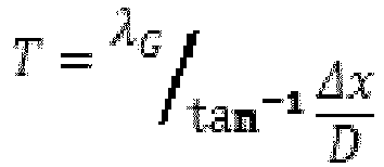

- For pixelated displays similar to that illustrated schematically in
Fig. 3 , where the pixel duty factor along the X direction is approximately 33%, desired pixel image shifts Δx will typically approximate the following relation
transparent cover 30, and that sparkle reduction should be balanced against pixel blurring, it is contemplated that the diffraction grating period T may be selected to provide a pixel image shift Δx that is either slightly greater than or slightly less than, i.e., within ± 10% of, 1/3 of the pixel size x in order to balance sparkle reduction and blurring. Preferred diffraction elements are typically characterized by a diffraction periods T between approximately 5 microns and approximately 50 microns. When the periodic structure has more than three orders of diffraction, the extreme orders of diffraction must have higher amplitudes than the central orders in order to achieve the same homogeneous image spread. - Some typical grating periods corresponding to different types of displays are listed in the Table 1 for gratings having three orders of diffraction. The grating period has been calculated for a wavelength λ of 530 nm.
Display Type Optical Distance, D (mm) Pixel Pitch (mm) Grating Period (µm) Laptop 1.0 0.191 8.35-16.2 Hand Held Device 2.4 0.194 19.8-39.6 Retina Display 1.2 0.078 24.5-49 - In high resolution displays, for example, the pixel size is about 75 µm. Optimizing the parameters of display system for green and assuming an optical distance D of 3 mm, the diffraction angle is 8.3 mRd (0.48 degrees) corresponding to a grating period of 63.8 µm. Assuming an air gap with refractive index n = 1 between the pixelated display and that the diffraction element comprises a periodic sinusoidal grating, the optimum amplitude of the roughness is 0.48 µm, which corresponds to a relatively shallow surface profile, i.e., the grating amplitude is about one hundredth of the grating period.
- In other embodiments, the diffraction element may comprise a random phase pattern. The random phase pattern may have a cutoff frequency such that the diffusion angular energy distribution is a rectangular distribution with a diffraction cone equal to the pixel size divided by the optical distance D from the pixel to the sparkle reduction surface.
- Although the various embodiments described herein relate primarily to diffraction elements obtained by surface texturing, it is contemplated that diffraction elements according to the present disclosure may also comprise components having bulk scattering properties. For example, the diffraction element may comprise a portion of transparent substrate in which the index of refraction of the transparent substrate has been modified, e.g., by ion exchange of a glass substrate through a mask, to create local variations in the index of refraction. When light propagates through the substrate, those local variations induce phase modulation into the optical waves, thus creating diffraction effects similar to surface texturing.
-
Fig. 3 also illustrates a preferred manner of orienting diffraction elements according to the present disclosure. Specifically,Fig 3 illustrates a multi-colored pixelated display where the display sub-pixels R, G, B are arranged within respective pixels of the display to define an anisotropic display, i.e., a display with fractional color component duty factors along the direction X and color component duty factors approaching 100% along the direction Y. For anisotropic displays, it is contemplated that the diffraction element of the sparkle reduction surface will preferably comprise a diffraction grating characterized by a grating period that is spaced along the direction X, as is illustrated schematically inFig. 3 . In this configuration, the greatest degree of sparkle reduction may be achieved without compromising too much image resolution. -
Fig. 2 illustrates an additional embodiment where a pixelated display 10' further comprises a partial index matching medium 40 contacting thesparkle reduction surface 34. For example, the partial index matching medium 40 may comprise an epoxy extending from thesparkle reduction surface 34 to thedisplay element 20. The partial index matching medium 40 is selected to have a refractive index that partially matches that of thediffraction element 38 in order to eliminate Fresnel reflections at the sparkle reduction surface and the surface of the display element. The partial index matching medium 40 has a refractive index that differs from that of thediffraction element 38 but defines an index contrast that is sufficiently low to attenuate the Fresnel reflection. At the same time, the index contrast is large enough to keep the roughness amplitude of thesparkle reduction surface 34 at reasonable levels. With an index contrast of 0.05, for example, the amplitude of the Fresnel reflection is around 0.04% and the ideal grating amplitudes are 4.8 µm and 3.4 µm for sinusoidal and square gratings, respectively. Given relatively large periods on the order of 20 µm to 40 µm, such amplitudes are achievable for grating manufacturing processes such as microlithography, embossing, replication, or the like. For example, it is contemplated that the partial index matching medium 40 and thesparkle reduction surface 34 of thetransparent display cover 30 may define an index contrast of between approximately 0.02 and approximately 0.3 and a reflection coefficient on the order of approximately 0.03%. - Referring to the expanded portion of
Fig. 1 , in some embodiments of the present disclosure, it may be preferable to engineer thediffraction element 38 such that the diffraction element depth b and the diffraction element index of refraction n1 are selected such that the phase modulation amplitude in reflection ΦR approximates an integer multiple of a given target wavelength, i.e., a wavelength λG between approximately 490 nm and approximately 570 nm, where
sparkle reduction surface 34. - It is noted that recitations herein of a component of the present disclosure being "configured" in a particular way, to embody a particular property, or function in a particular manner, are structural recitations, as opposed to recitations of intended use. More specifically, the references herein to the manner in which a component is "configured" denotes an existing physical condition of the component and, as such, is to be taken as a definite recitation of the structural characteristics of the component.
- It is noted that terms like "preferably," "commonly," and "typically," when utilized herein, are not utilized to limit the scope of the claimed invention or to imply that certain features are critical, essential, or even important to the structure or function of the claimed invention. Rather, these terms are merely intended to identify particular aspects of an embodiment of the present disclosure or to emphasize alternative or additional features that may or may not be utilized in a particular embodiment of the present disclosure.
- For the purposes of describing and defining the present disclosure it is noted that the terms "about" and "approximately" are utilized herein to represent the inherent degree of uncertainty that may be attributed to any quantitative comparison, value, measurement, or other representation. The terms "about" and "approximately" are also utilized herein to represent the degree by which a quantitative representation may vary from a stated reference without resulting in a change in the basic function of the subject matter at issue.
- Having described the subject matter of the present disclosure in detail and by reference to specific embodiments thereof, it is noted that the various details disclosed herein should not be taken to imply that these details relate to elements that are essential components of the various embodiments described herein, even in cases where a particular element is illustrated in each of the drawings that accompany the present description. Rather, the claims appended hereto should be taken as the sole representation of the breadth of the present disclosure and the corresponding scope of the various inventions described herein. Further, it will be apparent that modifications and variations are possible without departing from the scope of the invention defined in the appended claims. More specifically, although some aspects of the present disclosure are identified herein as preferred or particularly advantageous, it is contemplated that the present disclosure is not necessarily limited to these aspects.
- It is noted that one or more of the following claims utilize the term "wherein" as a transitional phrase. For the purposes of defining the present invention, it is noted that this term is introduced in the claims as an open-ended transitional phrase that is used to introduce a recitation of a series of characteristics of the structure and should be interpreted in like manner as the more commonly used open-ended preamble term "comprising."
- Embodiments of the invention include the following:
- [1] A multi-colored pixelated display comprising an image display element and a transparent display cover, wherein:
- the image display element comprises an array of display pixels each divided into a plurality of display sub-pixels each associated with a respective dedicated display color component, wherein the sub-pixels of a given color component, across multiple display pixels, form a sub-pixel array of that given color component;
- the transparent display cover comprises a display surface that is susceptible to marking and a sparkle reduction surface;
- the sparkle reduction surface is positioned between the image display element and the display surface along an optical path of the pixelated display and is spaced from the image display element by an optical distance D;
- the sparkle reduction surface comprises a texture that spreads in at least one direction the energy emitted by sub-pixels over a distance which, at the display surface, is larger than the size of a sub pixel and smaller than or equal to the pitch of the array of display pixels.
- [2] A multi-colored pixelated display as in [1] wherein respective sub-pixel arrays have a linear duty factor that varies according to the linear direction, along the array of display pixels, in which the linear duty factor is measured or calculated, and wherein said variation of the linear duty factor includes a minimum linear duty factor along a given linear direction, and wherein the energy emitted by sub-pixels is preferentially spread in the given linear direction.
- [3] A multi-colored pixelated display as in [1] wherein the texture is a diffractive element.
- [4] A multi-colored pixelated display as in [1] wherein:
- the image display element comprises an array of display pixels arranged at a pixel pitch x;
- the display sub-pixels of an individual display pixel are associated with a dedicated display color component, one of which lies at a wavelength λG between approximately 490 nm and approximately 570 nm;
- the diffraction element is characterized by a diffraction period T approximating the relation


- D is the optical distance from the pixels to the diffraction element, and
- x is the pixel pitch.
- [5] A multi-colored pixelated display as in [4] wherein the diffraction element is characterized by a diffraction period T where Δx = (⅓ ± 10%)x.
- [6] A multi-colored pixelated display as in [4] wherein the diffraction grating is characterized by a diffraction period T where Δx ≅ (a ± 10%)x and a represents an approximate duty factor of the dedicated display color component at the wavelength λG .
- [7] A multi-colored pixelated display as in [1] wherein the diffraction element is characterized by a diffraction period T between approximately 5 microns and approximately 50 microns.
- [8] A multi-colored pixelated display as in [1] wherein:
- the display sub-pixels are arranged within respective pixels to define an anisotropic display with fractional color component duty factors along a direction X; and
- the diffraction element of the sparkle reduction surface comprises a diffraction grating characterized by a grating period spaced along the direction X.
- [9] A multi-colored pixelated display as in [1] wherein:
- the display sub-pixels are arranged within respective pixels to define an anisotropic display with fractional color component duty factors along a direction X; and
- the diffraction element of the sparkle reduction surface comprises periodic diffraction elements spaced along the direction X.
- [10] A multi-colored pixelated display as in [1] wherein the display further comprises a partial index matching medium contacting the sparkle reduction surface and positioned along the optical path between the image display element and the transparent display cover.
- [11] A multi-colored pixelated display as in [10] wherein the partial index matching medium and the sparkle reduction surface of the transparent display cover define an index contrast of between approximately 0.02 and approximately 0.3 and a reflection coefficient on the order of approximately 0.03%.
- [12] A multi-colored pixelated display as in [1] wherein:
- the diffraction element of the sparkle reduction surface comprises periodic diffraction elements of depth b; and
- the diffraction element depth b and the diffraction element index of refraction n1 are selected such that the phase modulation amplitude in reflection ΦR approximates an integer multiple of a wavelength λG between approximately 490 nm and approximately 570 nm, where

- [13] A multi-colored pixelated display as in [1] wherein the diffraction element comprises a random phase pattern.
- [14] A multi-colored pixelated display as claimed in [13] wherein the random phase pattern defines a cutoff frequency selected such that a diffusion angular energy distribution of the diffraction element is a rectangular distribution with a diffraction cone equal to pixel size divided by the optical distance D.
- [15] A multi-colored pixelated display comprising an image display element and a transparent display cover, wherein:
- the image display element comprises an array of display pixels arranged at a pixel pitch x and divided into a plurality of display sub-pixels associated with respective dedicated display color components;
- the display sub-pixels of an individual display pixel are associated with a dedicated display color component, one of which lies at a wavelength λG between approximately 490 nm and approximately 570 nm;
- the transparent display cover comprises a display surface that is susceptible to marking and a sparkle reduction surface;
- the sparkle reduction surface is positioned between the image display element and the display surface along an optical path of the pixelated display and is spaced from the image display element by an optical distance D;
- the sparkle reduction surface comprises a micron grade diffraction element characterized by a diffraction period T approximating the relation


- [16] A multi-colored pixelated display as claimed in [15] wherein:
- the display sub-pixels are arranged within respective pixels to define an anisotropic display with fractional color component duty factors along a direction X; and
- the diffraction element of the sparkle reduction surface comprises periodic diffraction elements spaced along the direction X.
- [17] A multi-colored pixelated display as claimed in [15] wherein the display further comprises a partial index matching medium contacting the sparkle reduction surface and positioned along the optical path between the image display element and the transparent display cover, and wherein the phase modulation amplitude in reflection ΦR approximates an integer multiple of a wavelength λG between approximately 490 nm and approximately 570 nm, where Φ=2∗(n2-n1)b.
- [18] A multi-colored pixelated display as claimed in [17] wherein the partial index matching medium and the sparkle reduction surface of the transparent display cover define an index contrast of between approximately 0.02 and approximately 0.3 and a reflection coefficient on the order of approximately 0.03%.
Claims (4)
- A multi-colored pixelated display comprising an image display element and a transparent display cover, wherein:the image display element comprises an array of display pixels arranged at a pixel pitch x and divided into a plurality of display sub-pixels associated with respective dedicated display color components;the display sub-pixels of an individual display pixel are associated with a dedicated display color component, one of which lies at a wavelength λG between approximately 490 nm and approximately 570 nm;the transparent display cover comprises a display surface that is susceptible to marking and a sparkle reduction surface;the sparkle reduction surface is positioned between the image display element and the display surface along an optical path of the pixelated display and is spaced from the image display element by an optical distance D;the sparkle reduction surface comprises a micron grade diffraction element characterized by a diffraction period T approximating the relation


- A multi-colored pixelated display as claimed in claim 1 wherein:the display sub-pixels are arranged within respective pixels to define an anisotropic display with fractional color component duty factors along a direction X; andthe diffraction element of the sparkle reduction surface comprises periodic diffraction elements spaced along the direction X.
- A multi-colored pixelated display as claimed in claim 1 wherein the display further comprises a partial index matching medium contacting the sparkle reduction surface and positioned along the optical path between the image display element and the transparent display cover, and wherein the phase modulation amplitude in reflection ΦR approximates an integer multiple of a wavelength λG between approximately 490 nm and approximately 570 nm, where Φr=2∗(n2-n1)b.
- A multi-colored pixelated display as claimed in claim 3 wherein the partial index matching medium and the sparkle reduction surface of the transparent display cover define an index contrast of between approximately 0.02 and approximately 0.3 and a reflection coefficient on the order of approximately 0.03%.
Applications Claiming Priority (3)
| Application Number | Priority Date | Filing Date | Title |
|---|---|---|---|
| US201161561011P | 2011-11-17 | 2011-11-17 | |
| EP12849087.7A EP2780904B1 (en) | 2011-11-17 | 2012-11-06 | Multi-colored pixelated display with sparkle reduction surface |
| PCT/US2012/063657 WO2013074325A2 (en) | 2011-11-17 | 2012-11-06 | Multi-colored pixelated display with sparkle reduction surface |
Related Parent Applications (2)
| Application Number | Title | Priority Date | Filing Date |
|---|---|---|---|
| EP12849087.7A Division EP2780904B1 (en) | 2011-11-17 | 2012-11-06 | Multi-colored pixelated display with sparkle reduction surface |
| EP12849087.7A Division-Into EP2780904B1 (en) | 2011-11-17 | 2012-11-06 | Multi-colored pixelated display with sparkle reduction surface |
Publications (3)
| Publication Number | Publication Date |
|---|---|
| EP3608709A1 true EP3608709A1 (en) | 2020-02-12 |
| EP3608709B1 EP3608709B1 (en) | 2025-01-08 |
| EP3608709C0 EP3608709C0 (en) | 2025-01-08 |
Family
ID=48426260
Family Applications (2)
| Application Number | Title | Priority Date | Filing Date |
|---|---|---|---|
| EP19200745.8A Active EP3608709B1 (en) | 2011-11-17 | 2012-11-06 | Multi-colored pixelated display with a diffractive element |
| EP12849087.7A Active EP2780904B1 (en) | 2011-11-17 | 2012-11-06 | Multi-colored pixelated display with sparkle reduction surface |
Family Applications After (1)
| Application Number | Title | Priority Date | Filing Date |
|---|---|---|---|
| EP12849087.7A Active EP2780904B1 (en) | 2011-11-17 | 2012-11-06 | Multi-colored pixelated display with sparkle reduction surface |
Country Status (7)
| Country | Link |
|---|---|
| US (1) | US9454031B2 (en) |
| EP (2) | EP3608709B1 (en) |
| JP (3) | JP2015507754A (en) |
| KR (1) | KR102105576B1 (en) |
| CN (1) | CN104254883B (en) |
| TW (1) | TWI594048B (en) |
| WO (1) | WO2013074325A2 (en) |
Families Citing this family (22)
| Publication number | Priority date | Publication date | Assignee | Title |
|---|---|---|---|---|
| US9535280B2 (en) * | 2011-05-27 | 2017-01-03 | Corning Incorporated | Engineered antiglare surface to reduce display sparkle |
| KR101615332B1 (en) | 2012-03-06 | 2016-04-26 | 삼성디스플레이 주식회사 | Pixel arrangement structure for organic light emitting display device |
| US10832616B2 (en) | 2012-03-06 | 2020-11-10 | Samsung Display Co., Ltd. | Pixel arrangement structure for organic light emitting diode display |
| KR101427593B1 (en) | 2013-04-26 | 2014-08-07 | 삼성디스플레이 주식회사 | Organic light emitting diode display |
| US9995944B2 (en) | 2014-06-13 | 2018-06-12 | 3M Innovative Properties Company | Optical stacks for sparkle reduction |
| WO2015191949A1 (en) * | 2014-06-13 | 2015-12-17 | 3M Innovative Properties Company | Optical stacks for sparkle reduction |
| US9862124B2 (en) | 2014-07-18 | 2018-01-09 | 3M Innovative Properties Company | Multilayer optical adhesives and methods of making same |
| CN107003557B (en) | 2014-10-07 | 2023-05-30 | 康宁股份有限公司 | Direct-view display device and light unit for direct-view display device |
| DE102015212223B3 (en) * | 2015-06-30 | 2016-08-11 | Continental Automotive Gmbh | Method for controlling a display device for a vehicle |
| US10613727B2 (en) | 2016-02-19 | 2020-04-07 | Ppg Industries Ohio, Inc. | Color and texture match ratings for optimal match selection |
| CN105911711B (en) | 2016-06-24 | 2019-03-15 | 京东方科技集团股份有限公司 | a display device |
| US11378723B2 (en) | 2017-06-02 | 2022-07-05 | 3M Innovative Properties Company | Optical film and optical system |
| CN110770844A (en) | 2017-06-23 | 2020-02-07 | 3M创新有限公司 | Patient warming system with monitoring and feedback |
| KR102418724B1 (en) | 2017-12-05 | 2022-07-08 | 삼성디스플레이 주식회사 | Display device and mehthod for manufacturing the same |
| WO2019126151A1 (en) | 2017-12-20 | 2019-06-27 | 3M Innovative Properties Company | Structured optical surface and optical imaging system |
| FI129113B (en) | 2017-12-22 | 2021-07-15 | Dispelix Oy | Waveguide display and display element with novel grating configuration |
| US10877214B2 (en) * | 2018-05-04 | 2020-12-29 | Facebook Technologies, Llc | Diffraction gratings for beam redirection |
| KR102650669B1 (en) * | 2018-07-19 | 2024-03-26 | 삼성디스플레이 주식회사 | Display apparatus |
| TWI783875B (en) * | 2022-02-18 | 2022-11-11 | 友達光電股份有限公司 | Display panel |
| US12578506B2 (en) | 2022-04-29 | 2026-03-17 | 3M Innovative Properties Company | Optical film for the reduction of optical artifacts |
| CN118655722B (en) * | 2023-08-01 | 2025-04-29 | 华为技术有限公司 | Optical module, display device, display equipment and electronic equipment |
| CN118829322B (en) * | 2024-06-28 | 2025-03-28 | 华为技术有限公司 | Display modules and electronic devices |
Citations (2)
| Publication number | Priority date | Publication date | Assignee | Title |
|---|---|---|---|---|
| US5755501A (en) * | 1994-08-31 | 1998-05-26 | Omron Corporation | Image display device and optical low-pass filter |
| WO2012166407A1 (en) * | 2011-05-27 | 2012-12-06 | Corning Incorporated | Engineered antiglare surface to reduce display sparkle |
Family Cites Families (20)
| Publication number | Priority date | Publication date | Assignee | Title |
|---|---|---|---|---|
| KR0120397B1 (en) * | 1992-04-28 | 1997-10-22 | 나카무라 히사오 | Image display apparatus |
| EP0647327B1 (en) * | 1992-06-24 | 1998-03-04 | BRITISH TELECOMMUNICATIONS public limited company | Photoinduced grating in b2o3 containing glass |
| JPH0792026A (en) * | 1993-09-22 | 1995-04-07 | Matsushita Electric Ind Co Ltd | Pyroelectric infrared sensor |
| JPH08122710A (en) * | 1994-08-31 | 1996-05-17 | Omron Corp | Image display device and optical low-pass filter |
| JPH09325204A (en) * | 1996-05-31 | 1997-12-16 | Sony Corp | Optical filter, image display device and liquid crystal display device using the same |
| JPH10177107A (en) * | 1996-12-17 | 1998-06-30 | Hitachi Koki Co Ltd | Diffraction grating and optical recording device |
| JPH10253951A (en) * | 1997-03-14 | 1998-09-25 | Omron Corp | Reflective LCD |
| GB2340281A (en) * | 1998-08-04 | 2000-02-16 | Sharp Kk | A reflective liquid crystal display device |
| JP2000155286A (en) * | 1998-11-24 | 2000-06-06 | Olympus Optical Co Ltd | Video display device |
| JP4548754B2 (en) * | 1999-03-08 | 2010-09-22 | 大日本印刷株式会社 | Hologram photographing dry plate and image forming method using the same |
| JP2003215314A (en) * | 2002-01-18 | 2003-07-30 | Dainippon Printing Co Ltd | Anti-reflective articles |
| JP4183444B2 (en) * | 2002-05-29 | 2008-11-19 | アルプス電気株式会社 | Optical member |
| JP3993870B2 (en) * | 2002-06-10 | 2007-10-17 | 松下電器産業株式会社 | Compound objective lens, optical head device, optical information device, computer, optical disk player, car navigation system, optical disk recorder, optical disk server |
| US7321466B2 (en) * | 2005-02-11 | 2008-01-22 | Wasatch Photonics, Inc. | High dispersion diffraction grating including multiple holographic optical elements |
| JP2007328096A (en) * | 2006-06-07 | 2007-12-20 | Ricoh Co Ltd | Diffractive optical element, manufacturing method thereof, and optical module |
| US7944598B2 (en) * | 2008-11-06 | 2011-05-17 | Corning Incorporated | Speckle mitigation in laser scanner projector systems |
| US8130433B2 (en) | 2009-04-29 | 2012-03-06 | Corning Incorporated | Spinning optics for speckle mitigation in laser projection systems |
| CN102037399A (en) * | 2009-05-29 | 2011-04-27 | 松下电器产业株式会社 | Liquid crystal display device |
| JP5852956B2 (en) * | 2009-06-23 | 2016-02-03 | シーリアル テクノロジーズ ソシエテ アノニムSeereal Technologies S.A. | Light modulation device used for at least one of two-dimensional and three-dimensional image content display |
| US8598771B2 (en) * | 2009-09-15 | 2013-12-03 | Corning Incorporated | Glass and display having anti-glare properties |
-
2012
- 2012-10-15 US US13/651,652 patent/US9454031B2/en active Active
- 2012-11-06 EP EP19200745.8A patent/EP3608709B1/en active Active
- 2012-11-06 KR KR1020147014556A patent/KR102105576B1/en active Active
- 2012-11-06 EP EP12849087.7A patent/EP2780904B1/en active Active
- 2012-11-06 WO PCT/US2012/063657 patent/WO2013074325A2/en not_active Ceased
- 2012-11-06 JP JP2014542334A patent/JP2015507754A/en active Pending
- 2012-11-06 CN CN201280056637.1A patent/CN104254883B/en active Active
- 2012-11-08 TW TW101141566A patent/TWI594048B/en active
-
2018
- 2018-09-10 JP JP2018168522A patent/JP6731209B2/en active Active
-
2020
- 2020-07-03 JP JP2020115348A patent/JP7148218B2/en active Active
Patent Citations (2)
| Publication number | Priority date | Publication date | Assignee | Title |
|---|---|---|---|---|
| US5755501A (en) * | 1994-08-31 | 1998-05-26 | Omron Corporation | Image display device and optical low-pass filter |
| WO2012166407A1 (en) * | 2011-05-27 | 2012-12-06 | Corning Incorporated | Engineered antiglare surface to reduce display sparkle |
Also Published As
| Publication number | Publication date |
|---|---|
| WO2013074325A3 (en) | 2014-12-04 |
| EP2780904A2 (en) | 2014-09-24 |
| JP2015507754A (en) | 2015-03-12 |
| EP2780904B1 (en) | 2020-04-08 |
| WO2013074325A2 (en) | 2013-05-23 |
| KR20140096328A (en) | 2014-08-05 |
| EP2780904A4 (en) | 2015-12-23 |
| EP3608709B1 (en) | 2025-01-08 |
| EP3608709C0 (en) | 2025-01-08 |
| US20130127689A1 (en) | 2013-05-23 |
| JP6731209B2 (en) | 2020-07-29 |
| JP2019023738A (en) | 2019-02-14 |
| KR102105576B1 (en) | 2020-05-04 |
| TWI594048B (en) | 2017-08-01 |
| TW201329567A (en) | 2013-07-16 |
| CN104254883A (en) | 2014-12-31 |
| JP7148218B2 (en) | 2022-10-05 |
| US9454031B2 (en) | 2016-09-27 |
| JP2020184088A (en) | 2020-11-12 |
| CN104254883B (en) | 2017-03-29 |
Similar Documents
| Publication | Publication Date | Title |
|---|---|---|
| EP3608709B1 (en) | Multi-colored pixelated display with a diffractive element | |
| EP2715440B1 (en) | Engineered antiglare surface to reduce display sparkle | |
| US20250026111A1 (en) | Decorative sheet and display device | |
| JP7200949B2 (en) | Transparent display and laminated glass with transparent display | |
| JP6259791B2 (en) | Dual panel display with cross BEF collimator and polarization preserving diffuser | |
| EP2906991B1 (en) | Display devices having an antiglare layer providing reduced sparkle appearance | |
| CN110462287A (en) | Single sided backlight, multiview display and method employing tilted diffraction grating | |
| JP2014517931A5 (en) | ||
| US20130176619A1 (en) | Display apparatus | |
| CN113039390A (en) | Multi-view backlight, display and method with optical mask elements | |
| KR102253605B1 (en) | Optical sheet, backlight unit, liquid crystal display device, and information equipment | |
| US20100128464A1 (en) | Light diffusion plate, method for manufacturing the same and backlight assembly having the same | |
| WO2014074406A2 (en) | Films for display covers and display devices comprising the same | |
| TW201326919A (en) | A display device | |
| US9389456B2 (en) | Liquid crystal display | |
| JP7488307B2 (en) | Display device | |
| US20170212283A1 (en) | Display module and head mounted display using the same | |
| US20130083259A1 (en) | Optical enhancement for display touchscreen systems | |
| HK40050717A (en) | Multiview backlight, display, and method having optical mask elements | |
| HK40008090A (en) | Multiview backlighting employing fluorescent multibeam elements |
Legal Events
| Date | Code | Title | Description |
|---|---|---|---|
| PUAI | Public reference made under article 153(3) epc to a published international application that has entered the european phase |
Free format text: ORIGINAL CODE: 0009012 |
|
| STAA | Information on the status of an ep patent application or granted ep patent |
Free format text: STATUS: THE APPLICATION HAS BEEN PUBLISHED |
|
| AC | Divisional application: reference to earlier application |
Ref document number: 2780904 Country of ref document: EP Kind code of ref document: P |
|
| AK | Designated contracting states |
Kind code of ref document: A1 Designated state(s): AL AT BE BG CH CY CZ DE DK EE ES FI FR GB GR HR HU IE IS IT LI LT LU LV MC MK MT NL NO PL PT RO RS SE SI SK SM TR |
|
| STAA | Information on the status of an ep patent application or granted ep patent |
Free format text: STATUS: REQUEST FOR EXAMINATION WAS MADE |
|
| 17P | Request for examination filed |
Effective date: 20201111 |
|
| RBV | Designated contracting states (corrected) |
Designated state(s): AL AT BE BG CH CY CZ DE DK EE ES FI FR GB GR HR HU IE IS IT LI LT LU LV MC MK MT NL NO PL PT RO RS SE SI SK SM TR |
|
| STAA | Information on the status of an ep patent application or granted ep patent |
Free format text: STATUS: EXAMINATION IS IN PROGRESS |
|
| 17Q | First examination report despatched |
Effective date: 20220216 |
|
| GRAP | Despatch of communication of intention to grant a patent |
Free format text: ORIGINAL CODE: EPIDOSNIGR1 |
|
| STAA | Information on the status of an ep patent application or granted ep patent |
Free format text: STATUS: GRANT OF PATENT IS INTENDED |
|
| RIC1 | Information provided on ipc code assigned before grant |
Ipc: G02B 5/02 20060101ALI20240723BHEP Ipc: G02B 5/18 20060101ALI20240723BHEP Ipc: G02F 1/1335 20060101AFI20240723BHEP |
|
| INTG | Intention to grant announced |
Effective date: 20240805 |
|
| RIN1 | Information on inventor provided before grant (corrected) |
Inventor name: GOLLIER, JACQUES |
|
| GRAS | Grant fee paid |
Free format text: ORIGINAL CODE: EPIDOSNIGR3 |
|
| GRAA | (expected) grant |
Free format text: ORIGINAL CODE: 0009210 |
|
| STAA | Information on the status of an ep patent application or granted ep patent |
Free format text: STATUS: THE PATENT HAS BEEN GRANTED |
|
| AC | Divisional application: reference to earlier application |
Ref document number: 2780904 Country of ref document: EP Kind code of ref document: P |
|
| AK | Designated contracting states |
Kind code of ref document: B1 Designated state(s): AL AT BE BG CH CY CZ DE DK EE ES FI FR GB GR HR HU IE IS IT LI LT LU LV MC MK MT NL NO PL PT RO RS SE SI SK SM TR |
|
| REG | Reference to a national code |
Ref country code: GB Ref legal event code: FG4D |
|
| REG | Reference to a national code |
Ref country code: CH Ref legal event code: EP |
|
| REG | Reference to a national code |
Ref country code: DE Ref legal event code: R096 Ref document number: 602012081317 Country of ref document: DE |
|
| REG | Reference to a national code |
Ref country code: IE Ref legal event code: FG4D |
|
| U01 | Request for unitary effect filed |
Effective date: 20250207 |
|
| U07 | Unitary effect registered |
Designated state(s): AT BE BG DE DK EE FI FR IT LT LU LV MT NL PT RO SE SI Effective date: 20250213 |
|
| PG25 | Lapsed in a contracting state [announced via postgrant information from national office to epo] |
Ref country code: RS Free format text: LAPSE BECAUSE OF FAILURE TO SUBMIT A TRANSLATION OF THE DESCRIPTION OR TO PAY THE FEE WITHIN THE PRESCRIBED TIME-LIMIT Effective date: 20250408 |
|
| PG25 | Lapsed in a contracting state [announced via postgrant information from national office to epo] |
Ref country code: PL Free format text: LAPSE BECAUSE OF FAILURE TO SUBMIT A TRANSLATION OF THE DESCRIPTION OR TO PAY THE FEE WITHIN THE PRESCRIBED TIME-LIMIT Effective date: 20250108 |
|
| PG25 | Lapsed in a contracting state [announced via postgrant information from national office to epo] |
Ref country code: ES Free format text: LAPSE BECAUSE OF FAILURE TO SUBMIT A TRANSLATION OF THE DESCRIPTION OR TO PAY THE FEE WITHIN THE PRESCRIBED TIME-LIMIT Effective date: 20250108 |
|
| PG25 | Lapsed in a contracting state [announced via postgrant information from national office to epo] |
Ref country code: IS Free format text: LAPSE BECAUSE OF FAILURE TO SUBMIT A TRANSLATION OF THE DESCRIPTION OR TO PAY THE FEE WITHIN THE PRESCRIBED TIME-LIMIT Effective date: 20250508 Ref country code: NO Free format text: LAPSE BECAUSE OF FAILURE TO SUBMIT A TRANSLATION OF THE DESCRIPTION OR TO PAY THE FEE WITHIN THE PRESCRIBED TIME-LIMIT Effective date: 20250408 |
|
| PG25 | Lapsed in a contracting state [announced via postgrant information from national office to epo] |
Ref country code: HR Free format text: LAPSE BECAUSE OF FAILURE TO SUBMIT A TRANSLATION OF THE DESCRIPTION OR TO PAY THE FEE WITHIN THE PRESCRIBED TIME-LIMIT Effective date: 20250108 |
|
| PG25 | Lapsed in a contracting state [announced via postgrant information from national office to epo] |
Ref country code: GR Free format text: LAPSE BECAUSE OF FAILURE TO SUBMIT A TRANSLATION OF THE DESCRIPTION OR TO PAY THE FEE WITHIN THE PRESCRIBED TIME-LIMIT Effective date: 20250409 |
|
| PG25 | Lapsed in a contracting state [announced via postgrant information from national office to epo] |
Ref country code: SM Free format text: LAPSE BECAUSE OF FAILURE TO SUBMIT A TRANSLATION OF THE DESCRIPTION OR TO PAY THE FEE WITHIN THE PRESCRIBED TIME-LIMIT Effective date: 20250108 |
|
| PG25 | Lapsed in a contracting state [announced via postgrant information from national office to epo] |
Ref country code: CZ Free format text: LAPSE BECAUSE OF FAILURE TO SUBMIT A TRANSLATION OF THE DESCRIPTION OR TO PAY THE FEE WITHIN THE PRESCRIBED TIME-LIMIT Effective date: 20250108 |
|
| PG25 | Lapsed in a contracting state [announced via postgrant information from national office to epo] |
Ref country code: SK Free format text: LAPSE BECAUSE OF FAILURE TO SUBMIT A TRANSLATION OF THE DESCRIPTION OR TO PAY THE FEE WITHIN THE PRESCRIBED TIME-LIMIT Effective date: 20250108 |
|
| PLBE | No opposition filed within time limit |
Free format text: ORIGINAL CODE: 0009261 |
|
| STAA | Information on the status of an ep patent application or granted ep patent |
Free format text: STATUS: NO OPPOSITION FILED WITHIN TIME LIMIT |
|
| REG | Reference to a national code |
Ref country code: CH Ref legal event code: L10 Free format text: ST27 STATUS EVENT CODE: U-0-0-L10-L00 (AS PROVIDED BY THE NATIONAL OFFICE) Effective date: 20251119 |
|
| U20 | Renewal fee for the european patent with unitary effect paid |
Year of fee payment: 14 Effective date: 20251014 |
|
| 26N | No opposition filed |
Effective date: 20251009 |
|
| REG | Reference to a national code |
Ref country code: CH Ref legal event code: H13 Free format text: ST27 STATUS EVENT CODE: U-0-0-H10-H13 (AS PROVIDED BY THE NATIONAL OFFICE) Effective date: 20260623 |
|
| PG25 | Lapsed in a contracting state [announced via postgrant information from national office to epo] |
Ref country code: MC Free format text: LAPSE BECAUSE OF FAILURE TO SUBMIT A TRANSLATION OF THE DESCRIPTION OR TO PAY THE FEE WITHIN THE PRESCRIBED TIME-LIMIT Effective date: 20250108 |
|
| PG25 | Lapsed in a contracting state [announced via postgrant information from national office to epo] |
Ref country code: CH Free format text: LAPSE BECAUSE OF NON-PAYMENT OF DUE FEES Effective date: 20251130 |