JP2007328096A - Diffraction optical element, manufacturing method thereof and optical module - Google Patents
Diffraction optical element, manufacturing method thereof and optical module Download PDFInfo
- Publication number
- JP2007328096A JP2007328096A JP2006158469A JP2006158469A JP2007328096A JP 2007328096 A JP2007328096 A JP 2007328096A JP 2006158469 A JP2006158469 A JP 2006158469A JP 2006158469 A JP2006158469 A JP 2006158469A JP 2007328096 A JP2007328096 A JP 2007328096A
- Authority
- JP
- Japan
- Prior art keywords
- optical element
- diffractive optical
- periodic structure
- wavelength
- element according
- Prior art date
- Legal status (The legal status is an assumption and is not a legal conclusion. Google has not performed a legal analysis and makes no representation as to the accuracy of the status listed.)
- Pending
Links
Images


Abstract
Description
本発明は、撮像光学系、投影光学系、画像処理装置などの各種の光学機器に応用することが可能な回折光学素子および光学モジュールに関するものであり、より詳しくは、複数の波長あるいは特定の波長範囲で使用する回折光学素子、特に可視光全域で高い回折効率を有する回折光学素子と、その回折光学素子の作製方法、および、前記回折光学素子を有する光学モジュールに関するものである。 The present invention relates to a diffractive optical element and an optical module that can be applied to various optical devices such as an imaging optical system, a projection optical system, and an image processing apparatus. More specifically, the present invention relates to a plurality of wavelengths or specific wavelengths. The present invention relates to a diffractive optical element used in a range, in particular, a diffractive optical element having high diffraction efficiency over the entire visible light range, a method for manufacturing the diffractive optical element, and an optical module having the diffractive optical element.
従来、光の屈折を利用した素子としてレンズやプリズムなどが存在したが、回折光学素子はこれらの機能を平板構造で達成可能ため、小型軽量化を実現することができるものである。また、ビーム分岐や強度分布変換など、従来の屈折を利用した光学素子では実現不可能であった機能を持つ素子を作ることも可能である。これらの機能を有する回折光学素子としては、例えば図16に示すような透明材料12の表面に凹凸の形状を刻んだ構造13によって達成される(これを、以下、表面レリーフ型回折光学素子とする)。
Conventionally, lenses, prisms, and the like existed as elements utilizing light refraction, but diffractive optical elements can achieve these functions with a flat plate structure, and thus can be reduced in size and weight. It is also possible to make an element having a function that could not be realized by a conventional optical element using refraction, such as beam branching or intensity distribution conversion. As a diffractive optical element having these functions, for example, it is achieved by a
しかしながら、図16に示す表面レリーフ型の回折光学素子11は単一波長で設計されるものであり、図17に示すように、設計波長と異なる波長の光に対して用いると、回折効率が低下し光の利用効率が下がる、あるいは結像光学系ではフレアとなり画像品質を劣化させる、といった問題があった。
However, the surface relief type diffractive
これに関して、数式を用いて説明すると以下のようになる。
素子を通過する光の位相変調量の最大値φは、
φ=(n−1)d/λ 式(2)
で表される。
ここで、nは材料の屈折率、dはレリーフ構造の最大深さである。これを用い、m次の回折効率ηmは、以下の式(3) のように表される。
This will be described below using mathematical formulas.
The maximum value φ of the phase modulation amount of light passing through the element is
φ = (n−1) d / λ Equation (2)
It is represented by
Here, n is the refractive index of the material, and d is the maximum depth of the relief structure. Using this, the m-th order diffraction efficiency η m is expressed by the following equation (3).
よって、φの波長依存性により、回折効率は図17に示したとおり設計波長以外で低下することがわかる。
この問題を解決し、広い波長域で利用可能とした回折光学素子が特許文献1(特許第3717555号公報)に提案されている。
Therefore, it can be seen that due to the wavelength dependence of φ, the diffraction efficiency decreases at a wavelength other than the design wavelength as shown in FIG.
A diffractive optical element that solves this problem and can be used in a wide wavelength range is proposed in Patent Document 1 (Japanese Patent No. 3717555).
特許文献1に記載の従来技術では、図18に示すように、表面レリーフ型の構造23を有する第一の光学材料22(屈折率n1)の上に、屈折率および波長分散の異なる第二の光学材料24(屈折率n2)を積層することで、広い波長域で効率が高い回折光学素子21が得られることが示されている。この構造では、位相変調量の最大値φが以下の式(4) で表される。
In the prior art described in
これによれば、設計波長をλ0、設計波長以外の使用したい任意の波長をλとすれば、λにおける位相変調量φ(λ)は、以下の式(5) で表される。 According to this, if the design wavelength is λ 0 and an arbitrary wavelength other than the design wavelength to be used is λ, the phase modulation amount φ (λ) at λ is expressed by the following equation (5).
この位相変調量φ(λ)の波長依存性を表面レリーフ型回折光学素子よりも減らすためには、次の式(6) の条件を満たす屈折率材料を選択することで達成できる。
ただし、λ1>λ>λ2:λ1,λ2はそれぞれ使用波長の下限および上限の光の波長である。
In order to reduce the wavelength dependency of the phase modulation amount φ (λ) as compared with the surface relief type diffractive optical element, it can be achieved by selecting a refractive index material that satisfies the following equation (6).
However, λ 1 >λ> λ 2 : λ 1 and λ 2 are the lower and upper light wavelengths of the used wavelength, respectively.
また、近年、格子周期が使用波長よりも短い微細周期構造(以下、これをサブ波長構造と呼ぶ)による回折光学素子が特許文献2(特許第3547665号公報)などで提案されている。このようなサブ波長構造も、通常は単一波長で用いられるものであるが、広い波長域で高い光利用効率を得る手段が特許文献3(特開2001−343512公報)に記載されている。この特許文献3に記載の従来技術では、サブ波長構造に異種材料を埋め込むことで、広い波長域で効率が高い回折光学素子が得られることが示されている。
In recent years, a diffractive optical element having a fine periodic structure whose grating period is shorter than a used wavelength (hereinafter referred to as a sub-wavelength structure) has been proposed in Patent Document 2 (Japanese Patent No. 3547665). Such a subwavelength structure is also usually used at a single wavelength, but Patent Document 3 (Japanese Patent Laid-Open No. 2001-343512) describes means for obtaining high light utilization efficiency in a wide wavelength range. In the prior art described in
前述の従来技術のように、広い波長域で高い回折効率を得るためには、異なる材料を2つ以上用いる方法が採られてきた。このような方法において、広い波長範囲において高い回折効率を得るためには、複数の材料で分散特性を厳密に最適化する必要があり、既存の材料中からこのような条件を探し出すことは困難であった。 In order to obtain high diffraction efficiency in a wide wavelength range as in the above-described conventional technology, a method using two or more different materials has been adopted. In such a method, in order to obtain high diffraction efficiency in a wide wavelength range, it is necessary to strictly optimize the dispersion characteristics of a plurality of materials, and it is difficult to find such conditions from existing materials. there were.
本発明は上記事情に鑑みなされたものであり、第1の課題は、従来技術の問題を解決し、より自由度の高い設計が可能であり、かつ広い波長域でより高い回折効率を有する回折光学素子を提供することである。 The present invention has been made in view of the above circumstances, and a first problem is to solve the problems of the prior art, enable a design with a higher degree of freedom, and have a higher diffraction efficiency in a wide wavelength range. It is to provide an optical element.
また、本発明の第2の課題は、より作製が容易で、広い波長域で高い回折効率を有する回折光学素子を提供することであり、第3の課題は、特定の偏光に対してのみ、広い波長域で高い回折効率を有する回折光学素子を提供することであり、第4の課題は、無偏光な光に対して、広い波長域で高い回折効率を有する回折光学素子を提供することである。 The second problem of the present invention is to provide a diffractive optical element that is easier to manufacture and has a high diffraction efficiency in a wide wavelength range, and the third problem is only for specific polarized light. A fourth problem is to provide a diffractive optical element having a high diffraction efficiency in a wide wavelength range with respect to non-polarized light. is there.
ところで、通常の光学素子は、表面において入射面と出射面の屈折率の違いから生じるフレネル反射によるロスが存在する。フレネル反射は素子の面ごとで生じ、光利用効率の低下、迷光の発生によるフレア、などの原因となっていた。そこで表面反射の影響を低減させるため、単層の反射防止膜、あるいは誘電体膜を多層重ねた多層反射防止膜が一般的に利用される。しかしながら、このような膜によって広い波長域、広い入射角度で反射防止を行うことは容易ではなく、これを達成するためには高精度な膜制御が必要であり、高コストとなるものであった。
そこで本発明の第5の課題は、このような問題を解決し、広い波長域で表面反射が低減されている、高効率な回折光学素子を提供することである。
By the way, a normal optical element has a loss due to Fresnel reflection caused by a difference in refractive index between an incident surface and an exit surface on the surface. Fresnel reflection occurs on each surface of the element, causing a decrease in light utilization efficiency, flare due to generation of stray light, and the like. Therefore, in order to reduce the influence of surface reflection, a single-layer antireflection film or a multilayer antireflection film in which a plurality of dielectric films are stacked is generally used. However, it is not easy to prevent reflection with such a film in a wide wavelength range and a wide incident angle, and in order to achieve this, high-precision film control is necessary and the cost is high. .
Accordingly, a fifth problem of the present invention is to solve such a problem and provide a highly efficient diffractive optical element in which surface reflection is reduced in a wide wavelength range.
回折レンズはアッベ数が負の値を持つことから、屈折レンズと組み合わせて使用することで効率的に色収差の補正が可能であることが知られている。これに関しては、例えば非特許文献1(デジタル回折光学 丸善 p.360-363)に記載されている。
しかしながら、通常の回折レンズでは単一波長で良い回折効率を有し、他の波長では回折効率が低いため、フレアや色むら、光利用効率の低下、などの原因となっていた。
そこで本発明の第6の課題は、このような問題を解決し、広い波長域で高い回折効率を有する回折光学素子(例えば回折レンズ)を提供することである。
It is known that a diffractive lens has a negative Abbe number, so that it can efficiently correct chromatic aberration when used in combination with a refractive lens. This is described, for example, in Non-Patent Document 1 (Digital Diffraction Optics Maruzen p. 360-363).
However, a normal diffractive lens has good diffraction efficiency at a single wavelength and low diffraction efficiency at other wavelengths, causing flare, uneven color, and reduced light utilization efficiency.
Accordingly, a sixth problem of the present invention is to solve such a problem and provide a diffractive optical element (for example, a diffractive lens) having high diffraction efficiency in a wide wavelength region.
さらに本発明の第7の課題は、広い波長域で利用可能な、ビーム分岐機能を有する回折光学素子を提供することであり、第8の課題は、広い波長域で利用可能な、ビーム偏向機能を有する回折光学素子を提供することであり、第9の課題は、広い波長域で利用可能な、ビーム整形機能を有する回折光学素子を提供することであり、第10の課題は、偏光依存性が低く、広い波長域で高い回折効率を有する回折光学素子を提供することであり、第11の課題は、設計が容易で、広い波長域で回折効率の高い回折光学素子を提供することである。 The seventh object of the present invention is to provide a diffractive optical element having a beam branching function that can be used in a wide wavelength range, and the eighth problem is a beam deflection function that can be used in a wide wavelength range. The ninth problem is to provide a diffractive optical element having a beam shaping function that can be used in a wide wavelength range, and the tenth problem is polarization dependence. Is to provide a diffractive optical element having a low diffraction rate and a high diffraction efficiency in a wide wavelength range, and an eleventh problem is to provide a diffractive optical element that is easy to design and has a high diffraction efficiency in a wide wavelength range. .
前述の特許文献1や特許文献3などに記載の、従来の広い波長域で利用可能な回折光学素子は、いずれも複数の材料を用いて作製されるものであった。しかしながら、複数の材料を用いることは、材料費、製造方法の複雑化、などの面から製造に時間がかかり、コストが高くなるものであった。
そこで本発明の第12の課題は、低コストで生産性に優れる、広い波長域で利用可能な回折光学素子を提供することである。
All of the conventional diffractive optical elements that can be used in a wide wavelength range described in
Accordingly, a twelfth problem of the present invention is to provide a diffractive optical element that can be used in a wide wavelength range and is low in cost and excellent in productivity.
さらに本発明の第13の課題は、より高い機能を有した回折光学素子を提供することであり、第14の課題は、より耐久性の高い回折光学素子、あるいは光利用効率のより高い回折光学素子など、より高機能な回折光学素子を提供することである。
また、本発明の第15の課題は、量産性に優れた回折光学素子の作製方法を提供することである。
さらに本発明の第16の課題は、高機能であり、かつ小型・軽量化された光学モジュールを提供することである。
The thirteenth problem of the present invention is to provide a diffractive optical element having a higher function, and the fourteenth problem is a diffractive optical element with higher durability or diffractive optical with higher light utilization efficiency. It is to provide a higher-performance diffractive optical element such as an element.
A fifteenth problem of the present invention is to provide a method for manufacturing a diffractive optical element excellent in mass productivity.
Furthermore, a sixteenth problem of the present invention is to provide an optical module that is highly functional and that is small and light.
上記の課題を解決するため、本発明では以下のような手段を採っている。
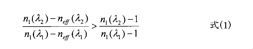
本発明の第1の手段は、表面にレリーフパターンが形成されている回折光学素子において、前記レリーフパターン上に、使用する波長の最小波長よりも短いピッチを有する微細周期構造が形成されており、前記レリーフパターン部の屈折率n1および、前記微細周期構造部における有効屈折率neffが、次の式(1) を満たすことを特徴とする。
In order to solve the above problems, the present invention adopts the following means.
According to a first means of the present invention, in the diffractive optical element having a relief pattern formed on the surface, a fine periodic structure having a pitch shorter than the minimum wavelength of the wavelength to be used is formed on the relief pattern, The refractive index n 1 of the relief pattern portion and the effective refractive index n eff of the fine periodic structure portion satisfy the following expression (1).
本発明の第2の手段は、第1の手段の回折光学素子において、前記微細周期構造のピッチおよび幅が全範囲にわたって略等しいことを特徴とする。
また、本発明の第3の手段は、第1または第2の手段の回折光学素子において、前記微細周期構造が、素子平面内で略等しい高さになるよう形成されていることを特徴とする。
According to a second means of the present invention, in the diffractive optical element of the first means, the pitch and width of the fine periodic structure are substantially equal over the entire range.
According to a third means of the present invention, in the diffractive optical element of the first or second means, the fine periodic structure is formed so as to have substantially the same height in the element plane. .
本発明の第4の手段は、第1乃至第3のいずれか1つの手段の回折光学素子において、前記微細周期構造が、1次元の格子周期構造となっていることを特徴とする。
また、本発明の第5の手段は、第1乃至第3のいずれか1つの手段の回折光学素子において、前記微細周期構造が、柱状または空孔の2次元アレイ状周期構造となっていることを特徴とする。
さらに本発明の第6の手段は、第1乃至第5のいずれか1つの手段の回折光学素子において、前記微細周期構造は、表面側がより細くなっていることを特徴とする。
According to a fourth means of the present invention, in the diffractive optical element of any one of the first to third means, the fine periodic structure is a one-dimensional grating periodic structure.
According to a fifth means of the present invention, in the diffractive optical element of any one of the first to third means, the fine periodic structure is a two-dimensional array structure having a columnar shape or a hole. It is characterized by.
Further, a sixth means of the present invention is the diffractive optical element of any one of the first to fifth means, wherein the fine periodic structure is thinner on the surface side.
本発明の第7の手段は、第1乃至第6のいずれか1つの手段の回折光学素子において、前記レリーフパターンは、同心円状の構造であることを特徴とする。
また、本発明の第8の手段は、第1乃至第6のいずれか1つの手段の回折光学素子において、前記レリーフパターンは、1次元または2次元の周期構造であることを特徴とする。
さらに本発明の第9の手段は、第1乃至第6のいずれか1つの手段の回折光学素子において、前記レリーフパターンは、鋸歯状の構造であることを特徴とする。
さらにまた、本発明の第10の手段は、第1乃至第6のいずれか1つの手段の回折光学素子において、前記レリーフパターンが、所定の形状にビームを整形するよう設計された構造であることを特徴とする。
According to a seventh means of the present invention, in the diffractive optical element of any one of the first to sixth means, the relief pattern has a concentric structure.
According to an eighth means of the present invention, in the diffractive optical element of any one of the first to sixth means, the relief pattern has a one-dimensional or two-dimensional periodic structure.
The ninth means of the present invention is the diffractive optical element of any one of the first to sixth means, wherein the relief pattern has a sawtooth structure.
Still further, according to a tenth means of the present invention, in the diffractive optical element of any one of the first to sixth means, the relief pattern is a structure designed to shape the beam into a predetermined shape. It is characterized by.
本発明の第11の手段は、表面にレリーフパターンが形成されている回折光学素子において、前記レリーフパターン上に、使用する波長の最小波長よりも短いピッチを有する微細周期構造が等ピッチで2次元周期状に形成されていることを特徴とする。
また、本発明の第12の手段は、第1乃至第11のいずれか1つの手段の回折光学素子において、2種類以上の材料によって形成されていることを特徴とする。
さらに本発明の第13の手段は、第1乃至第11のいずれか1つの手段の回折光学素子において、単一の材料により形成されていることを特徴とする。
According to an eleventh means of the present invention, in the diffractive optical element having a relief pattern formed on the surface, a fine periodic structure having a pitch shorter than the minimum wavelength of the wavelength to be used is two-dimensionally arranged at an equal pitch on the relief pattern. It is characterized by being formed periodically.
According to a twelfth means of the present invention, in the diffractive optical element of any one of the first to eleventh means, the diffractive optical element is formed of two or more kinds of materials.
Further, a thirteenth means of the present invention is characterized in that in the diffractive optical element of any one of the first to eleventh means, the diffractive optical element is formed of a single material.
本発明の第14の手段は、第1乃至第13のいずれか1つの手段の回折光学素子において、少なくとも1面が曲面であることを特徴とする。
また、本発明の第15の手段は、第1乃至第14のいずれか1つの手段の回折光学素子において、少なくとも1面に薄膜層が形成されていることを特徴とする。
According to a fourteenth means of the present invention, in the diffractive optical element of any one of the first to thirteenth means, at least one surface is a curved surface.
According to a fifteenth means of the present invention, in the diffractive optical element of any one of the first to fourteenth means, a thin film layer is formed on at least one surface.
本発明の第16の手段は、第1乃至第15のいずれか1つの手段の回折光学素子を作製する作製方法において、前記回折光学素子の構造を作製する際に、高さが空間的に異なる1次元または2次元の周期構造を有する構造体を型として、該型の形状を転写する工程が含まれていることを特徴とする。 According to a sixteenth means of the present invention, in the production method for producing a diffractive optical element according to any one of the first to fifteenth means, the height of the diffractive optical element is spatially different when producing the structure of the diffractive optical element. The method includes a step of transferring a shape of a mold having a structure having a one-dimensional or two-dimensional periodic structure as a mold.
本発明の第17の手段は、光学モジュールであって、第1乃至第15のいずれか1つの手段の回折光学素子と、少なくとも1枚以上のレンズと、受光素子とを有することを特徴とする。 A seventeenth means of the present invention is an optical module, comprising the diffractive optical element of any one of the first to fifteenth means, at least one lens, and a light receiving element. .
前述の従来技術では、複数の材料の分散特性を合わせこむ必要があり困難であったが、第1の手段の回折光学素子においては、微細周期構造のピッチ、幅、高さ(または深さ)などのパラメータを変えることにより微細周期構造における有効屈折率の波長依存性を調整することが可能であり、前記の式(1) を満たすようにすることにより、所望の複数波長あるいは波長範囲において回折効率がより高い回折光学素子を実現することが可能となり、また、より自由に設計することが可能な回折光学素子を提供することが可能となる。 In the prior art described above, it is difficult to match the dispersion characteristics of a plurality of materials. However, in the diffractive optical element of the first means, the pitch, width, and height (or depth) of the fine periodic structure are difficult. It is possible to adjust the wavelength dependence of the effective refractive index in a fine periodic structure by changing parameters such as the above, and by satisfying the above equation (1), diffraction is performed at a desired multiple wavelengths or wavelength range. A diffractive optical element with higher efficiency can be realized, and a diffractive optical element that can be designed more freely can be provided.
第2の手段の回折光学素子においては、第1の手段の構成および効果に加え、微細周期構造のピッチおよび幅が略一定となっていることで、より製造が容易な構造とすることが可能である。 In the diffractive optical element of the second means, in addition to the configuration and effects of the first means, the pitch and width of the fine periodic structure are substantially constant, so that the structure can be made easier to manufacture. It is.
第3の手段の回折光学素子においては、第1または第2の手段の構成及び効果に加え、素子表面内で略等しい高さとすることで、より製造が容易な構造とすることが可能である。これは以下のような理由による。
本発明の回折光学素子の構造を作製するには、凸部の高さが等しいため、凹部のみ深さを制御して作製してやれば良い。よって、リソグラフィによって本発明の形状を作製するには、基板上に平坦に塗布されたレジストに対して、凹部を形成したい箇所に深さに応じて強度を調整した電子線を照射し、現像した後に、エッチングを行えばよい。あるいは、転写によって本発明の構造を作製する際に、型となる構造は底面が等しく高さが異なる構造となる。このような型構造は底面と高さの両方が異なる構造に対して作製が容易である。
In the diffractive optical element of the third means, in addition to the configuration and effect of the first or second means, it is possible to make the structure easier to manufacture by making the height substantially equal within the element surface. . This is due to the following reasons.
In order to fabricate the structure of the diffractive optical element of the present invention, since the heights of the convex portions are equal, only the concave portions may be fabricated by controlling the depth. Therefore, in order to produce the shape of the present invention by lithography, a resist applied flatly on a substrate was developed by irradiating an electron beam whose intensity was adjusted according to the depth at a portion where a recess was desired to be formed. Etching may be performed later. Alternatively, when the structure of the present invention is manufactured by transfer, the structure to be a mold is a structure having the same bottom surface and different height. Such a mold structure is easy to manufacture for structures having different bottoms and heights.
第4の手段の回折光学素子においては、第1乃至第3のいずれか1つの手段の構成および効果に加え、前記微細周期構造が、1次元の格子周期構造となっているが、1次元周期構造では、有効屈折率が偏光方向によって異なる。これにより、ある一つの偏光状態に対して最適化された回折光学素子構造では、異なる偏光では高い回折効率を持たないので、偏光に対して効率の異なる偏光依存の回折光学素子が可能となる。 In the diffractive optical element of the fourth means, in addition to the configuration and effect of any one of the first to third means, the fine periodic structure is a one-dimensional grating periodic structure. In the structure, the effective refractive index varies depending on the polarization direction. As a result, a diffractive optical element structure optimized for a certain polarization state does not have high diffraction efficiency for different polarized light, and thus a polarization-dependent diffractive optical element having different efficiency for polarized light is possible.
第5の手段の回折光学素子においては、第1乃至第3のいずれか1つの手段の構成および効果に加え、前記微細周期構造が、柱状または空孔の2次元アレイ状周期構造となっているが、2次元アレイ状周期構造では、有効屈折率に偏光による違いが無い。このため、どのような偏光状態の光に対しても使用可能な、広帯域・高効率回折光学素子を実現することが可能となる。 In the diffractive optical element of the fifth means, in addition to the configuration and effect of any one of the first to third means, the fine periodic structure is a two-dimensional array structure of columns or holes. However, in the two-dimensional array periodic structure, there is no difference in the effective refractive index due to polarization. For this reason, it is possible to realize a broadband and high-efficiency diffractive optical element that can be used for light of any polarization state.
第6の手段の回折光学素子においては、第1乃至第5のいずれか1つの手段の構成および効果に加え、前記微細周期構造は、表面側がより細くなっていることにより、広い波長域に対して表面反射をよく低減することが可能となる。これによって、光利用効率がより高い回折光学素子を得ることができる。 In the diffractive optical element of the sixth means, in addition to the configuration and effect of any one of the first to fifth means, the fine periodic structure has a narrower surface side, so that it has a wider wavelength range. Thus, the surface reflection can be reduced well. Thereby, a diffractive optical element with higher light utilization efficiency can be obtained.
第7の手段の回折光学素子においては、第1乃至第6のいずれか1つの手段の構成および効果に加え、前記レリーフパターンは、同心円状の構造であることにより、回折レンズとして機能させることができる。
回折レンズはアッベ数が負の値を持つことから、屈折レンズと組み合わせて使用することで効率的に色収差の補正が可能であることが知られているが、第7の手段の回折光学素子は、広い波長域で高い回折効率を有する素子であり、フレアや色むらや光利用効率の低下が少ない回折レンズとして使用可能である。
In the diffractive optical element of the seventh means, in addition to the configuration and effect of any one of the first to sixth means, the relief pattern has a concentric structure, so that it can function as a diffractive lens. it can.
A diffractive lens has a negative Abbe number, and it is known that chromatic aberration can be efficiently corrected by using it in combination with a refractive lens. It is an element having high diffraction efficiency in a wide wavelength region, and can be used as a diffraction lens with little flare, color unevenness, and reduction in light utilization efficiency.
第8の手段の回折光学素子においては、第1乃至第6のいずれか1つの手段の構成および効果に加え、前記レリーフパターンは、1次元または2次元の周期構造であることにより、広帯域・高効率なビームスプリッタとして機能させることができる。
また、第9の手段の回折光学素子においては、第1乃至第6のいずれか1つの手段の構成および効果に加え、前記レリーフパターンは、鋸歯状の構造であることにより、広帯域・高効率なグレーティングとして機能させることができる。これによって、透過型の素子によって分光することが可能となり、分光光学系の小型化を達成することも可能である。
In the diffractive optical element of the eighth means, in addition to the configuration and effect of any one of the first to sixth means, the relief pattern has a one-dimensional or two-dimensional periodic structure, so It can function as an efficient beam splitter.
In the diffractive optical element of the ninth means, in addition to the configuration and effect of any one of the first to sixth means, the relief pattern has a sawtooth structure, so that it has a wide bandwidth and high efficiency. It can function as a grating. Accordingly, it is possible to perform spectroscopy using a transmissive element, and it is also possible to reduce the size of the spectroscopic optical system.
第10の手段の回折光学素子においては、第1乃至第6のいずれか1つの手段の構成および効果に加え、前記レリーフパターンが、所定の形状にビームを整形するよう設計された構造であることにより、特定の波長範囲あるいは複数の波長を有する光に対して、高い光利用効率で任意の形状に整形することが可能となる。
このような構造は特に白色光をいわゆるトップハットなビームパターンに均質化するときに有効である。また、波長によって均質領域のずれが生じるが、中心部では広い波長域で均質化された領域を得ることができる。
In the diffractive optical element of the tenth means, in addition to the structure and effect of any one of the first to sixth means, the relief pattern has a structure designed to shape the beam into a predetermined shape. Thus, it becomes possible to shape light having a specific wavelength range or a plurality of wavelengths into an arbitrary shape with high light utilization efficiency.
Such a structure is particularly effective when homogenizing white light into a so-called top-hat beam pattern. Moreover, although the shift | offset | difference of a homogeneous area | region arises with a wavelength, the area | region homogenized in the wide wavelength range can be obtained in the center part.
第11の手段の回折光学素子においては、レリーフパターン上に、使用する波長の最小波長よりも短いピッチを有する微細周期構造が等ピッチで2次元周期状に形成されていることにより、より容易に作製可能な構造であり、かつ広い波長域で高い回折効率を有する回折光学素子を提供することが可能となる。また、本発明の回折光学素子は偏光依存性を持たないため、太陽光、ランプの発光、発光ダイオード(LED)の発光、といった無偏光であり、かつ波長域に幅を有する光に対して高い光利用効率で用いることができる。つまり、カメラや投影装置、分光装置など、様々な光学機器に対して利用可能となる。そして、光学機器内部にこのような回折光学素子を用いることで、機器の軽量化、小型化を達成することができる。 In the diffractive optical element of the eleventh means, the fine periodic structure having a pitch shorter than the minimum wavelength of the wavelength to be used is formed on the relief pattern in a two-dimensional periodic shape at an equal pitch, thereby making it easier. It is possible to provide a diffractive optical element having a structure that can be manufactured and having high diffraction efficiency in a wide wavelength range. In addition, since the diffractive optical element of the present invention has no polarization dependency, it is non-polarized light such as sunlight, light emitted from a lamp, light emitted from a light emitting diode (LED), and is high with respect to light having a width in a wavelength region. It can be used with light utilization efficiency. That is, it can be used for various optical devices such as a camera, a projection device, and a spectroscopic device. By using such a diffractive optical element inside the optical device, it is possible to reduce the weight and size of the device.
第12の手段の回折光学素子においては、第1乃至第11のいずれか1つの手段の構成および効果に加え、2種類以上の材料によって形成されていることにより、より設計の自由度が増し、より高効率の回折光学素子を実現することができる。
また、第13の手段の回折光学素子においては、第1乃至第11のいずれか1つの手段の構成および効果に加え、単一の材料で構成されることにより、型からの転写による作製が可能となり、量産性に優れた回折光学素子を実現することができる。
In the diffractive optical element of the twelfth means, in addition to the configuration and effect of any one of the first to eleventh means, the diffractive optical element is formed of two or more types of materials, thereby increasing the degree of freedom in design. A more efficient diffractive optical element can be realized.
The diffractive optical element of the thirteenth means can be manufactured by transfer from a mold by being composed of a single material in addition to the structure and effect of any one of the first to eleventh means. Thus, a diffractive optical element having excellent mass productivity can be realized.
第14の手段の回折光学素子においては、第1乃至第13のいずれか1つの手段の構成および効果に加え、少なくとも1面が曲面であることにより、回折光学素子としての機能に加えて屈折レンズとしての機能を加えることが可能になる。本発明の回折光学素子では、例えば、広い波長域で高い回折効率を有する回折レンズと、屈折レンズが1枚の構成として提供可能である。これによって、光学系のレンズ枚数を減らすことができ、より小型・軽量化を達成することが可能となる。 In the diffractive optical element of the fourteenth means, in addition to the structure and effect of any one of the first to thirteenth means, at least one surface is a curved surface, so that in addition to the function as a diffractive optical element, a refractive lens It becomes possible to add the function as. In the diffractive optical element of the present invention, for example, a diffractive lens having a high diffraction efficiency in a wide wavelength region and a refractive lens can be provided as a single configuration. As a result, the number of lenses in the optical system can be reduced, and further reduction in size and weight can be achieved.
第15の手段の回折光学素子においては、第1乃至第14のいずれか1つの手段の構成および効果に加え、少なくとも1面に薄膜層が形成されていることにより、より耐久性・信頼性に優れた回折光学素子とすることが可能になる。あるいは、多層膜による光学的な機能を付け加えることも可能であり、より高機能な回折光学素子とすることができる。 In the diffractive optical element of the fifteenth means, in addition to the configuration and effect of any one of the first to fourteenth means, a thin film layer is formed on at least one surface, so that durability and reliability are further improved. An excellent diffractive optical element can be obtained. Alternatively, an optical function by a multilayer film can be added, and a higher-performance diffractive optical element can be obtained.
第16の手段の回折光学素子の作製方法においては、第1乃至第15のいずれか1つの手段の回折光学素子の構造を作製する際に、高さが空間的に異なる1次元または2次元の周期構造を有する構造体を型として、該型の形状を転写する工程が含まれていることにより、広い波長域で高い回折効率を有する回折光学素子を、容易に低コストで大量に生産することが可能となる。 In the diffractive optical element manufacturing method of the sixteenth means, when the structure of the diffractive optical element of any one of the first to fifteenth means is manufactured, the one-dimensional or two-dimensional height is spatially different. By using a structure having a periodic structure as a mold and transferring the shape of the mold, diffractive optical elements having high diffraction efficiency in a wide wavelength range can be easily produced in large quantities at low cost. Is possible.
第17の手段の光学モジュールにおいては、第1乃至第15のいずれか1つの手段の回折光学素子と、少なくとも1枚以上のレンズと、受光素子とを有することにより、カメラや分光器などの種々の光学機器に使用可能な、小型・軽量化された光学モジュールを提供することが可能となる。 The optical module of the seventeenth means includes a diffractive optical element of any one of the first to fifteenth means, at least one lens, and a light receiving element, so that various cameras and spectroscopes can be used. It is possible to provide a compact and light-weight optical module that can be used in such optical equipment.
以下、本発明の構成、動作および作用効果を図示の実施例に基づいて詳細に説明する。なお、図示の実施例は模式的に表したものであり、正確な寸法を表すものではない。 Hereinafter, the configuration, operation, and effects of the present invention will be described in detail based on the illustrated embodiments. In addition, the Example of illustration is represented typically and does not represent an exact dimension.
[実施例1]
まず、第1〜第4、第9、第12、第13の手段に係る回折光学素子の実施例について説明する。
本発明の回折光学素子に用いる波長以下の微細周期構造(以下、サブ波長構造と呼ぶ)に関して、その特性を図1のような1次元周期構造を用いて説明する。図1は本発明に係る回折光学素子101の1次元周期構造102の断面を模式的に表した断面図である。通常、図1に示すような周期構造102に光を入射した際には、回折光が生じる。この回折光の回折角θは、入射光の波長をλ、周期構造102のピッチをpとして以下のような式(7) で表される。ここで、mはm次の回折光を表す。
sinθ=mλ/p 式(7)
[Example 1]
First, examples of the diffractive optical element according to the first to fourth, ninth, twelfth, and thirteenth means will be described.
The characteristics of a fine periodic structure having a wavelength shorter than that used in the diffractive optical element of the present invention (hereinafter referred to as a sub-wavelength structure) will be described using a one-dimensional periodic structure as shown in FIG. FIG. 1 is a cross-sectional view schematically showing a cross section of a one-dimensional
sinθ = mλ / p Equation (7)
式(7) より、周期構造102のピッチpが波長λよりも短いときには回折角が実解を持たず、すなわち回折しないことがわかる。このとき、入射光に対して周期構造102は有効屈折率neffを持つ均質な媒質として表すことができることが知られている。例えば非特許文献2(Sov.Phys.JETP 2 466-(1956))には、有効屈折率neffの近似的な解が示されている。これによれば、有効屈折率neffは波長依存性を有しており、また、サブ波長構造のピッチpやデューティを変えることにより有効屈折率の波長依存性が変化する。
From equation (7), it can be seen that when the pitch p of the
ここで、一例として、SCHOTT社製のガラス:LASF31(主屈折率nd=1.88、アッベ数νd=41)に関して、図1の周期構造の有効屈折率neffを図2に示す。各パラメータとして、ピッチp=300nm、周期構造の幅a=180nmとし、波長400nmから700nmの範囲において計算を行った。図2のグラフの破線は材料本来の屈折率、実線はTM偏光(電場の振動方向が周期方向に直角な成分)における周期構造の有効屈折率を表す。このように、有効屈折率は、材料本来の屈折率と異なる分散特性を有する。 Here, as an example, regarding the glass manufactured by SCHOTT: LASF31 (main refractive index nd = 1.88, Abbe number νd = 41), the effective refractive index n eff of the periodic structure of FIG. 1 is shown in FIG. As each parameter, the calculation was performed in the wavelength range of 400 nm to 700 nm with the pitch p = 300 nm and the width a of the periodic structure = 180 nm. The broken line in the graph of FIG. 2 represents the original refractive index of the material, and the solid line represents the effective refractive index of the periodic structure in TM polarized light (component in which the vibration direction of the electric field is perpendicular to the periodic direction). Thus, the effective refractive index has a dispersion characteristic different from the original refractive index of the material.
本発明では、サブ波長構造のこのような特性を利用することで、回折効率の波長依存性を改善することが可能であることを見出した。すなわち、材料の表面にレリーフパターンが形成されおり、レリーフパターン上にサブ波長構造が形成されている回折光学素子において、レリーフパターン部の屈折率n1およびサブ波長構造部における有効屈折率neffが、以下の式(1) を満たす構造によって、回折効率の波長依存性が改善可能である。また、サブ波長構造のピッチp、幅a、高さ(または深さ)dなどのパラメータを変えることによりサブ波長構造における有効屈折率の波長依存性を調整することが可能である。 In the present invention, it has been found that the wavelength dependence of diffraction efficiency can be improved by utilizing such characteristics of the sub-wavelength structure. That is, the relief pattern has been formed on the surface of the material, in the diffractive optical element that is sub-wavelength structure is formed on the relief pattern, the effective refractive index n eff in the refractive index n 1 and the sub-wavelength structure of the relief pattern portion The wavelength dependency of the diffraction efficiency can be improved by the structure satisfying the following formula (1). Further, the wavelength dependence of the effective refractive index in the sub-wavelength structure can be adjusted by changing parameters such as the pitch p, width a, and height (or depth) d of the sub-wavelength structure.
次に図1を用いて具体的な周期構造の例を以下に示す。
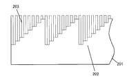
材料として、SCHOTT社製のガラス:LASF31(nd=1.88,νd=41)を例に設計を行った。サブ波長構造部としては前述したものと同じピッチp=300nm、周期構造の幅a=180nmとしたとき、その有効屈折率の波長依存性は前述したとおり図2となる。図3に、このピッチpと幅aを持つサブ波長構造203と階段状の表面レリーフ構造202とを組み合わせた構造を持つ回折光学素子201を示す。このような構造では、入射光を特定次数の回折光のみに集中させることが可能であり、すなわち入射光を特定の方向に偏向させることができる。
Next, an example of a specific periodic structure is shown below using FIG.
As a material, the design was performed by using glass made by SCHOTT: LASF31 (nd = 1.88, νd = 41) as an example. When the sub-wavelength structure portion has the same pitch p = 300 nm as described above and the width of the periodic structure a = 180 nm, the wavelength dependency of the effective refractive index is as shown in FIG. FIG. 3 shows a diffractive
図3に示す構造のTM偏光に対する1次光の回折効率の理論計算値を図4に示す。図4のグラフで実線は図3に示す構造の回折効率、点線は従来のサブ波長構造なしで最適化された表面レリーフ構造の回折効率である。このように、階段状の表面レリーフ構造202にサブ波長構造203を加えることにより、広帯域で回折効率の高い回折光学素子201を得ることができる。
このとき、TE偏光(TM偏光と直交する偏光成分)においては回折効率が最適化されておらず、TM偏光でのみ広い波長域で高い回折効率を有することになる。このように、特定の偏光のみに対して高い回折効率を有する回折光学素子が実現可能となる。
FIG. 4 shows a theoretical calculation value of the diffraction efficiency of the primary light with respect to the TM polarized light having the structure shown in FIG. In the graph of FIG. 4, the solid line represents the diffraction efficiency of the structure shown in FIG. 3, and the dotted line represents the diffraction efficiency of the surface relief structure optimized without the conventional subwavelength structure. Thus, by adding the
At this time, the diffraction efficiency is not optimized in the TE polarized light (polarized component orthogonal to the TM polarized light), and only the TM polarized light has a high diffraction efficiency in a wide wavelength region. Thus, a diffractive optical element having high diffraction efficiency for only specific polarized light can be realized.
ここで、レリーフ構造部とサブ波長構造部は同一の材料を用いて設計を行ったが、異なる材料を用いることも可能である。異なる材料を用いることで、より設計の自由度が増すため、より高効率な回折光学素子の設計も可能である。また、異なる材料によって形成される構造は、例えば次のような方法で作製することが可能である。
石英基板の表面にレリーフ構造をエッチングで形成した後に、光硬化性樹脂でレリーフ構造を埋め平坦化する。その後に微細周期構造状のパターンで露光を行い、光硬化性樹脂を硬化させた後に、未露光部を除去する。これによって、レリーフ構造部は石英で、サブ波長構造部が光硬化性樹脂で出来た構造が作製される。
Here, although the relief structure part and the subwavelength structure part were designed using the same material, it is also possible to use different materials. By using different materials, the degree of design freedom increases, so that it is possible to design a more efficient diffractive optical element. In addition, a structure formed of different materials can be manufactured by the following method, for example.
After the relief structure is formed on the surface of the quartz substrate by etching, the relief structure is filled with a photocurable resin and planarized. Thereafter, exposure is performed with a pattern having a fine periodic structure to cure the photocurable resin, and then the unexposed portion is removed. As a result, a structure in which the relief structure is made of quartz and the sub-wavelength structure is made of a photocurable resin is produced.
このような2種類の材料を用いた構造に対して、同一の材料を用いる利点としては、作製が容易となる点があげられる。単一材料によって作製するため、1回の転写によって、あるいはリソグラフィによってパターンを形成することが可能となり、量産性に優れた回折光学素子となる。 As an advantage of using the same material for such a structure using two types of materials, it can be easily manufactured. Since it is made of a single material, a pattern can be formed by one transfer or by lithography, and the diffractive optical element is excellent in mass productivity.
このように、同一材料を用いるか、異なる材料を用いるかは用途に応じて使い分けることが可能である。また、材料としてはガラス材料以外に、高分子樹脂や、金属酸化物を使用することが可能である。 In this way, it is possible to use the same material or different materials depending on the application. In addition to the glass material, a polymer resin or a metal oxide can be used as the material.
なお、このようなサブ波長構造は必ずしも等しいピッチおよび幅で全面形成されている必要は無く、ピッチあるいは幅、あるいはその両方が変調されていても良い。
また、このようなレリーフ構造あるいはサブ波長構造は、素子全面に形成されている必要は無く、光束有効範囲内の一部に形成されているものでも良い。あるいは、素子の両面にこのような構造が形成されているものでも良い。
Such a subwavelength structure is not necessarily formed on the entire surface with the same pitch and width, and the pitch and / or the width may be modulated.
Further, such a relief structure or sub-wavelength structure does not need to be formed on the entire surface of the element, and may be formed in a part of the effective light beam range. Alternatively, such a structure may be formed on both sides of the element.
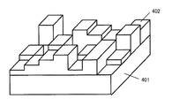
図3では、階段状のレリーフ構造202を示したが、図5に示す回折光学素子301のように、一般的によく使用される鋸歯状のような連続的形状のレリーフ構造302を用いても良く、このレリーフ構造302の上にサブ波長構造303を設ければ良い。また、図6に示す回折光学素子401のように、レリーフ構造402は凹凸が周期的な構造ではないものであっても良い。
なお、図3、図5では、サブ波長構造203,303が素子上で高さが等しくなるように示したが、素子全体の高さが空間的に異なる構造でも良い。
In FIG. 3, the step-shaped
3 and 5, the
[実施例2]
次に第5、第11の手段に係る回折光学素子の実施例について説明する。
2次元周期のサブ波長構造を用いた回折光学素子501の実施例の全体像を図7(a)に、その断面図を図7(b)に示す。ここでは構造は微細なピッチを有する2次元周期の円状ホールアレイ502が、空間的に深さが異なって配置されている構造となっている。このような2次元周期のサブ波長構造においても、前述した実施例1の1次元構造と同様に有効屈折率が波長依存性を示すことが非特許文献3(J.Opt.Soc.Am.A 15(6) 1577-1587 (1998))などに示されている。
よって、このような構造においても、広い波長域で高い回折効率を得ることが可能な回折光学素子を提供することができる。
[Example 2]
Next, examples of the diffractive optical element according to the fifth and eleventh means will be described.
FIG. 7A shows an overall image of an embodiment of the diffractive
Therefore, even in such a structure, a diffractive optical element capable of obtaining high diffraction efficiency in a wide wavelength region can be provided.
図7に示す実施例では、円筒形をした微細空孔が縦横に2次元アレイ状に並んでいるが、2次元アレイは六方細密に並んでいても良いし、他の並び方でも良い。また、空孔は円形である必要は無く、楕円形状や四角形状など様々な形状をとることが可能である。あるいは、周期構造が空孔である必要はなく、例えば図8に示す回折光学素子601のように、高さが空間的に異なるピラー形状の周期構造602でも良い。
In the embodiment shown in FIG. 7, the cylindrical fine holes are arranged in a two-dimensional array vertically and horizontally, but the two-dimensional array may be arranged in a hexagonal close-packed manner, or in other ways. The holes do not need to be circular, and can take various shapes such as an elliptical shape and a rectangular shape. Alternatively, the periodic structure does not need to be a hole, and may be a pillar-shaped
[実施例3]
次に第6の手段に係る回折光学素子の実施例について説明する。
本実施例の回折光学素子を図9に示す。この回折光学素子201は、図3と同様にサブ波長構造203と階段状の表面レリーフ構造202とを組み合わせた構造を持つが、サブ波長構造203の先端部に、先端が徐々に細くなった構造204が設けてある。このような構造とすることで、広い波長域の光に対して素子表面におけるフレネル反射を低減せしめることが可能となる。より望ましくは、サブ波長構造部203において、レリーフ構造202の最も高い点よりも上部で徐々に構造204が細くなっているのがよい。
[Example 3]
Next, examples of the diffractive optical element according to the sixth means will be described.
The diffractive optical element of this example is shown in FIG. The diffractive
このような構造は例えば以下のような方法で作製することが可能である。
石英基板上にレジストを塗布した後に、電子線の強度を変えながら露光を行う。レジストを現像すると、照射した電子線の強度に応じて微細な凹凸を有する構造が得られる。これをマスクとしてドライエッチングを行い、レジストの凹凸を石英上に転写する。このとき、ドライエッチングの条件を最適化することにより、先端部が細い形状を形成することが可能である。このようにして、図9に示したような、サブ波長構造203の先端部に、先端が徐々に細くなった構造204を作製することができる。なお、エッチングによって先端部がとがった錘形状を有する構造を作製する方法は、例えば特許文献4(特開2001−272505公報)に開示されている。
Such a structure can be produced, for example, by the following method.
After applying a resist on the quartz substrate, exposure is performed while changing the intensity of the electron beam. When the resist is developed, a structure having fine irregularities according to the intensity of the irradiated electron beam can be obtained. Using this as a mask, dry etching is performed to transfer the unevenness of the resist onto quartz. At this time, it is possible to form a shape with a thin tip by optimizing the dry etching conditions. In this manner, a
[実施例4]
次に第7、第14の手段に係る回折光学素子の実施例について説明する。
本実施例の回折光学素子701としては、図10(a)に示すように、レリーフ構造部702が同心円状のいわゆる回折レンズ形状を有している。また、レリーフ構造は量子化されていて、階段状の形状となっていてもよい。
このような回折レンズは、通常利用される屈折レンズと組み合わせることにより色収差を効率的に補正することが可能である。さらには、屈折系のレンズと本実施例の回折レンズとを一体化して、図10(b)に示すように、回折レンズ形状を有する面と反対側の面が曲面704を有した構造であると、その曲面704を屈折レンズ(レンズ面)として機能させることができ、レンズを別に設ける必要がなく、素子数を減らすことが可能となる。
[Example 4]
Next, examples of the diffractive optical element according to the seventh and fourteenth means will be described.
As the diffractive
Such a diffractive lens can efficiently correct chromatic aberration by combining it with a normally used refractive lens. Further, the refractive lens and the diffractive lens of the present embodiment are integrated, and the surface opposite to the surface having the diffractive lens shape has a
[実施例5]
次に第8の手段に係る回折光学素子の実施例について説明する。
本実施例の回折光学素子801を図11に示す。この回折光学素子801では、レリーフ構造802も周期構造をしており、その上にサブ波長構造803が設けられている。このような構造によって入射光は複数の光に分岐することができる。図11のようなレリーフ構造802を持つ回折光学素子801では、0次光と1次光、−1次光の3つに光を分岐することができ、レリーフ構造802の高さを最適に設定することで、3つの強度を同じにすることも可能である。また、レリーフ構造802を2次元的な周期構造とすることで、2次元的に光を分けることも可能である。
[Example 5]
Next, examples of the diffractive optical element according to the eighth means will be described.
A diffractive
[実施例6]
次に第10の手段に係る回折光学素子の実施例について説明する。
本実施例の回折光学素子は、レリーフパターンが図12(a)に示すような構造となっている。図12(a)はいわゆる計算機合成ホログラム(CGH)パターンであり、色の濃淡がレリーフパターンの深さを表しているものである。図12(a)の形状を有するレリーフパターン上にサブ波長構造が形成された回折光学素子では、白色の平行光が入射すると、特定の距離において、各波長における図12(b)のような形状が再生されることになる。このように、レリーフパターンにホログラムパターンを用いることで、ビームを任意の形状に整形することが可能な回折光学素子を作製することが可能である。
[Example 6]
Next, examples of the diffractive optical element according to the tenth means will be described.
In the diffractive optical element of this example, the relief pattern has a structure as shown in FIG. FIG. 12A shows a so-called computer-generated hologram (CGH) pattern, in which the shade of color represents the depth of the relief pattern. In the diffractive optical element in which the sub-wavelength structure is formed on the relief pattern having the shape of FIG. 12A, when white parallel light is incident, the shape as shown in FIG. 12B at each wavelength at a specific distance. Will be played. Thus, by using a hologram pattern as a relief pattern, a diffractive optical element capable of shaping a beam into an arbitrary shape can be manufactured.
なお、このようなホログラムパターンの形状を計算する方法には、反復フーリエ変換法やシミュレーテッドアニーリング法などを用いることが可能である。
これらの計算方法に関しては、それぞれ非特許文献4(Appl.Opt. 33,863-867 (1994))、非特許文献5(Opt.Eng. 19, 297-305 (1980))に詳しく記載されている。
反復フーリエ変換法は、大きな画素数のホログラムもシミュレーテッドアニーリング法に対して短時間で計算できるため、より好ましい。
As a method for calculating the shape of the hologram pattern, it is possible to use an iterative Fourier transform method or a simulated annealing method.
These calculation methods are described in detail in Non-Patent Document 4 (Appl. Opt. 33,863-867 (1994)) and Non-Patent Document 5 (Opt. Eng. 19, 297-305 (1980)), respectively.
The iterative Fourier transform method is more preferable because a hologram having a large number of pixels can be calculated in a short time compared to the simulated annealing method.
[実施例7]
次に第15の手段に係る回折光学素子の実施例について説明する。
本実施例の回折光学素子901は、図13(a)に示すように、微細なサブ波長構造902が形成されている面上に薄膜903が形成されている構造となっている。サブ波長構造902はアスペクトが比較的高い構造であるため傷つきやすい。これに対して、図13(a)に示すように、サブ波長構造902上に薄膜903が形成されていることで保護膜の役割を果たすことができ、信頼性・耐久性を向上させることが可能である。この薄膜903はどのような組成のものでも問題は無いが、使用波長域に対して透過率を有することが必要である。あるいは、単なる保護膜に限らず、誘電体や樹脂によって反射防止用の膜を形成することも可能である。あるいは、単層の膜ではなく、図12(b)に示すように多層膜904とすることで、バンドパスフィルタの機能や、偏光分離の機能などを付け加えることも可能であり、より高機能な素子とすることができる。これらの単層膜903や多層膜904は、構造が形成されていない面にも付け加えることができ、これによって回折光学素子を高機能化することができる。
[Example 7]
Next, examples of the diffractive optical element according to the fifteenth means will be described.
As shown in FIG. 13A, the diffractive
以上、本発明に係る回折光学素子の実施例を説明したが、これらの実施例で示した構造のサブ波長構造部は、すべて前述の式(1) の条件を満たす構造となっているものである。 As described above, the embodiments of the diffractive optical element according to the present invention have been described. However, the sub-wavelength structures having the structures shown in these embodiments all have a structure that satisfies the above-described expression (1). is there.
[実施例8]
次に第16の手段に係る回折光学素子の作製方法の実施例を図14を用いて説明する。
図14(a)に示すように、金属などによって形成された型1101を用い、これに樹脂等からなる転写材1102を流し込み、さらに転写材1102を硬化させた後に、型1101から離型することで、回折光学素子1103を容易に得ることが可能である。この方法は、型1101を1度作ることができれば、何度も再利用して転写することが可能であるため、非常に量産性に優れており、低コストな作製方法である。
転写材料としては、熱可塑性の樹脂、光硬化性の樹脂などの高分子材料の他、有機・無機の混合材料であるゾル・ゲル材料や、低融点ガラスなどを利用することができる。硬化方法は材料に対して最適なものが選ばれるものであるが、通常は熱インプリント法もしくは光インプリント法のどちらかが用いられる。熱インプリント法では、熱可塑性の材料を用い、高温で型に密着させた後に、温度を下げ離型を行う。光インプリント法では、光硬化性の樹脂またはゾル・ゲル材料などを用い、型に材料を流し込んだ後に、主に紫外線を照射することで材料を硬化させ、その後、離型を行う。
[Example 8]
Next, an embodiment of a method for producing a diffractive optical element according to the sixteenth means will be described with reference to FIG.
As shown in FIG. 14A, a
As the transfer material, a polymer material such as a thermoplastic resin or a photo-curable resin, a sol / gel material which is a mixed organic / inorganic material, a low melting point glass, or the like can be used. The curing method is selected to be optimal for the material, but usually either the thermal imprint method or the photoimprint method is used. In the thermal imprinting method, a thermoplastic material is used, and after being brought into close contact with the mold at a high temperature, the temperature is lowered to release the mold. In the photoimprint method, a photocurable resin or a sol / gel material is used, and after the material is poured into a mold, the material is cured mainly by irradiating ultraviolet rays, and then the mold release is performed.
型の作製方法としては図14(b)に示すような方法が考えられる。この方法では、基板1201上にレジスト材料1202を塗布し、電子線1203を場所によって強度を変えながら照射することで露光を行う。露光後、レジストを現像すると、照射した電子線の強度に応じて凹凸のあるレジスト1204が形成される。これに金属膜1205を蒸着し、電鋳を行った後、基板1201とレジスト1204を離型することで金属型1206が得られる。そして、この金属型1206を、図14(a)の型1101として用いれば、前述のようにして、回折光学素子1103を容易に得ることができる。なお、上記の型の作製方法は一例であり、この方法に限定されるものではない。
As a mold manufacturing method, a method as shown in FIG. In this method, exposure is performed by applying a resist
[実施例9]
次に第17の手段に係る光学モジュールの実施例について説明する。
上述したような実施例の回折光学素子は、他の光学素子と組み合わせることによって高機能でかつ小型・軽量な光学モジュールとして使用可能である。先に述べたように、屈折レンズと本発明の回折光学素子(例えば回折レンズ)とを組み合わせることで、効率的に色収差低減を行うことが可能な光学モジュールとすることができる。
[Example 9]
Next, an example of the optical module according to the seventeenth means will be described.
The diffractive optical element of the embodiment as described above can be used as an optical module having a high function, a small size, and a light weight when combined with other optical elements. As described above, by combining the refractive lens and the diffractive optical element of the present invention (for example, a diffractive lens), an optical module capable of efficiently reducing chromatic aberration can be obtained.
ここでは、光学モジュールの一実施例として、図15に示す光学モジュール5について説明する。図15において、回折光学素子1は、偏向機能を有するレリーフ構造にサブ波長構造が形成されており、可視光全域で高い回折効率を有する回折光学素子となっている。この構造の回折光学素子1の直後にレンズ2を設置し、集光点において受光素子(例えばラインセンサー)3が配置されている。これによって、複数の波長を有する入射光4は高い利用効率で分光され、ラインセンサー3上に波長ごとに異なる位置で集光される。このように、光利用効率が広い波長域で高く、小型で、分光機能を有する光学モジュール5を実現することができる。
Here, an
なお、図15は光学モジュールの一例であり、この構成に限るものではなく、実施例1〜7で説明した回折光学素子と、少なくとも1枚以上のレンズと、受光素子とを適宜組み合わせることにより、様々な機能を持った光学モジュールを構成することができる。
また、実施例1〜7で説明した回折光学素子や、それを用いた光学モジュールは、撮像光学系、投影光学系、画像処理装置などの各種の光学機器に応用することができる。
15 is an example of an optical module, and is not limited to this configuration. By appropriately combining the diffractive optical element described in Examples 1 to 7, at least one lens, and a light receiving element, An optical module having various functions can be configured.
In addition, the diffractive optical element described in
1:偏向機能を有する回折光学素子
2:レンズ
3:受光素子(ラインセンサー)
4:複数の波長を有する光
5:光学モジュール
101:回折光学素子
102:微細周期構造(サブ波長構造)
201:回折光学素子
202:階段状の表面レリーフ構造
203:サブ波長構造
204:先端が徐々に細くなった構造
301:回折光学素子
302:鋸歯状のレリーフ構造
303:サブ波長構造
401:回折光学素子
402:凹凸が周期的でないレリーフ構造
501:回折光学素子
502:円状ホールアレイ
601:回折光学素子
602:ピラー形状の周期構造
701:回折レンズ形状を有する回折光学素子
702:同心円状のレリーフ構造
703:サブ波長構造
704:曲面(レンズ面)
801:回折光学素子
802:周期構造のレリーフ構造
803:サブ波長構造
901:回折光学素子
902:サブ波長構造
903:単層の薄膜(単層膜)
904:多層膜
1101:型
1102:転写材
1103:回折光学素子
1201:基板
1202:レジスト材料
1203:電子線
1204:レジスト
1205:金属膜
1206:金属型
1: Diffractive optical element having a deflection function 2: Lens 3: Light receiving element (line sensor)
4: Light having a plurality of wavelengths 5: Optical module 101: Diffractive optical element 102: Fine periodic structure (sub-wavelength structure)
201: diffractive optical element 202: stepped surface relief structure 203: sub-wavelength structure 204: structure in which the tip is gradually narrowed 301: diffractive optical element 302: serrated relief structure 303: sub-wavelength structure 401: diffractive optical element 402: Relief structure where irregularities are not periodic 501: Diffractive optical element 502: Circular hole array 601: Diffractive optical element 602: Periodic structure of pillar shape 701: Diffractive optical element having a diffractive lens shape 702: Concentric relief structure 703 : Sub-wavelength structure 704: Curved surface (lens surface)
801: Diffractive optical element 802: Relief structure of periodic structure 803: Sub-wavelength structure 901: Diffractive optical element 902: Sub-wavelength structure 903: Single-layer thin film (single-layer film)
904: Multilayer film 1101: Mold 1102: Transfer material 1103: Diffraction optical element 1201: Substrate 1202: Resist material 1203: Electron beam 1204: Resist 1205: Metal film 1206: Metal mold
Claims (17)
前記レリーフパターン上に、使用する波長の最小波長よりも短いピッチを有する微細周期構造が形成されており、前記レリーフパターン部の屈折率n1および、前記微細周期構造部における有効屈折率neffが、次の式(1) を満たすことを特徴とする回折光学素子。
A fine periodic structure having a pitch shorter than the minimum wavelength of the wavelength to be used is formed on the relief pattern, and the refractive index n 1 of the relief pattern portion and the effective refractive index n eff in the fine periodic structure portion are A diffractive optical element satisfying the following formula (1):
前記微細周期構造のピッチおよび幅が全範囲にわたって略等しいことを特徴とする回折光学素子。 The diffractive optical element according to claim 1,
A diffractive optical element characterized in that the pitch and width of the fine periodic structure are substantially equal over the entire range.
前記微細周期構造が、素子平面内で略等しい高さになるよう形成されていることを特徴とする回折光学素子。 The diffractive optical element according to claim 1 or 2,
The diffractive optical element, wherein the fine periodic structure is formed to have substantially the same height in the element plane.
前記微細周期構造が、1次元の格子周期構造となっていることを特徴とする回折光学素子。 The diffractive optical element according to any one of claims 1 to 3,
The diffractive optical element, wherein the fine periodic structure is a one-dimensional grating periodic structure.
前記微細周期構造が、柱状または空孔の2次元アレイ状周期構造となっていることを特徴とする回折光学素子。 The diffractive optical element according to any one of claims 1 to 3,
2. The diffractive optical element according to claim 1, wherein the fine periodic structure is a columnar or vacant two-dimensional array periodic structure.
前記微細周期構造は、表面側がより細くなっていることを特徴とする回折光学素子。 The diffractive optical element according to any one of claims 1 to 5,
A diffractive optical element characterized in that the fine periodic structure has a thinner surface side.
前記レリーフパターンは、同心円状の構造であることを特徴とする回折光学素子。 The diffractive optical element according to any one of claims 1 to 6,
The diffractive optical element, wherein the relief pattern has a concentric structure.
前記レリーフパターンは、1次元または2次元の周期構造であることを特徴とする回折光学素子。 The diffractive optical element according to any one of claims 1 to 6,
The diffractive optical element, wherein the relief pattern has a one-dimensional or two-dimensional periodic structure.
前記レリーフパターンは、鋸歯状の構造であることを特徴とする回折光学素子。 The diffractive optical element according to any one of claims 1 to 6,
2. The diffractive optical element according to claim 1, wherein the relief pattern has a sawtooth structure.
前記レリーフパターンが、所定の形状にビームを整形するよう設計された構造であることを特徴とする回折光学素子。 The diffractive optical element according to any one of claims 1 to 6,
The diffractive optical element, wherein the relief pattern has a structure designed to shape a beam into a predetermined shape.
前記レリーフパターン上に、使用する波長の最小波長よりも短いピッチを有する微細周期構造が等ピッチで2次元周期状に形成されていることを特徴とする回折光学素子。 In a diffractive optical element having a relief pattern formed on the surface,
A diffractive optical element, wherein a fine periodic structure having a pitch shorter than a minimum wavelength of wavelengths to be used is formed on the relief pattern in a two-dimensional periodic shape at an equal pitch.
2種類以上の材料によって形成されていることを特徴とする回折光学素子。 The diffractive optical element according to any one of claims 1 to 11,
A diffractive optical element characterized by being formed of two or more kinds of materials.
単一の材料により形成されていることを特徴とする回折光学素子。 The diffractive optical element according to any one of claims 1 to 11,
A diffractive optical element characterized by being formed of a single material.
少なくとも1面が曲面であることを特徴とする回折光学素子。 The diffractive optical element according to any one of claims 1 to 13,
A diffractive optical element, wherein at least one surface is a curved surface.
少なくとも1面に薄膜層が形成されていることを特徴とする回折光学素子。 The diffractive optical element according to any one of claims 1 to 14,
A diffractive optical element, wherein a thin film layer is formed on at least one surface.
前記回折光学素子の構造を作製する際に、高さが空間的に異なる1次元または2次元の周期構造を有する構造体を型として、該型の形状を転写する工程が含まれていることを特徴とする回折光学素子の作製方法。 In the manufacturing method which manufactures the diffractive optical element of any one of Claims 1 thru | or 15,
The manufacturing of the structure of the diffractive optical element includes a step of transferring the shape of the mold using a structure having a one-dimensional or two-dimensional periodic structure with spatially different heights as a mold. A method for producing a diffractive optical element.
An optical module comprising the diffractive optical element according to any one of claims 1 to 15, at least one lens, and a light receiving element.
Priority Applications (1)
| Application Number | Priority Date | Filing Date | Title |
|---|---|---|---|
| JP2006158469A JP2007328096A (en) | 2006-06-07 | 2006-06-07 | Diffraction optical element, manufacturing method thereof and optical module |
Applications Claiming Priority (1)
| Application Number | Priority Date | Filing Date | Title |
|---|---|---|---|
| JP2006158469A JP2007328096A (en) | 2006-06-07 | 2006-06-07 | Diffraction optical element, manufacturing method thereof and optical module |
Publications (1)
| Publication Number | Publication Date |
|---|---|
| JP2007328096A true JP2007328096A (en) | 2007-12-20 |
Family
ID=38928617
Family Applications (1)
| Application Number | Title | Priority Date | Filing Date |
|---|---|---|---|
| JP2006158469A Pending JP2007328096A (en) | 2006-06-07 | 2006-06-07 | Diffraction optical element, manufacturing method thereof and optical module |
Country Status (1)
| Country | Link |
|---|---|
| JP (1) | JP2007328096A (en) |
Cited By (16)
| Publication number | Priority date | Publication date | Assignee | Title |
|---|---|---|---|---|
| JP2010197798A (en) * | 2009-02-26 | 2010-09-09 | Toppan Printing Co Ltd | Optical element having forgery prevention function and forgery prevention display body equipped with the same |
| JP2012215723A (en) * | 2011-04-01 | 2012-11-08 | Canon Inc | Optical element and imaging element |
| WO2012160662A1 (en) | 2011-05-25 | 2012-11-29 | 株式会社日立製作所 | Solar cell |
| KR20140096328A (en) * | 2011-11-17 | 2014-08-05 | 코닝 인코포레이티드 | Multi-colored pixelated display with sparkle reduction surface |
| JP2015018822A (en) * | 2014-09-24 | 2015-01-29 | パナソニックIpマネジメント株式会社 | Light emitting element |
| WO2018220271A1 (en) * | 2017-06-02 | 2018-12-06 | Dispelix Oy | Method of manufacturing a height-modulated optical diffractive grating |
| WO2018220264A1 (en) * | 2017-06-02 | 2018-12-06 | Dispelix Oy | Method of manufacturing a diffractive grating |
| KR20190058655A (en) * | 2016-10-18 | 2019-05-29 | 몰레큘러 임프린츠 인코퍼레이티드 | Micro lithography fabrication of structures |
| WO2019209527A1 (en) * | 2018-04-23 | 2019-10-31 | Facebook Technologies, Llc | Gratings with variable depths for waveguide displays |
| CN110998375A (en) * | 2017-06-02 | 2020-04-10 | 迪斯帕列斯有限公司 | Method for manufacturing mother plate and mother plate |
| US10649141B1 (en) | 2018-04-23 | 2020-05-12 | Facebook Technologies, Llc | Gratings with variable etch heights for waveguide displays |
| US10732351B2 (en) | 2018-04-23 | 2020-08-04 | Facebook Technologies, Llc | Gratings with variable depths formed using planarization for waveguide displays |
| CN111880254A (en) * | 2020-07-14 | 2020-11-03 | 浙江大学 | Preparation method of grating with continuously-changed diffraction efficiency |
| US20210194144A1 (en) * | 2019-12-20 | 2021-06-24 | Hamamatsu Photonics K.K. | Terahertz wave lens and method for producing terahertz wave lens |
| CN113500801A (en) * | 2021-07-12 | 2021-10-15 | 嘉兴驭光光电科技有限公司 | Diffraction-inhibiting optical element and manufacturing method thereof |
| US11774651B2 (en) | 2019-12-20 | 2023-10-03 | Hamamatsu Photonics K.K. | Terahertz wave optical element and method for producing terahertz wave optical element |
Citations (3)
| Publication number | Priority date | Publication date | Assignee | Title |
|---|---|---|---|---|
| JP2001343512A (en) * | 2000-05-31 | 2001-12-14 | Canon Inc | Diffraction optical device and optical system having the same |
| JP2003315526A (en) * | 2002-04-26 | 2003-11-06 | Konica Minolta Holdings Inc | Diffraction optical element and manufacturing method thereof |
| JP2005285305A (en) * | 2004-03-04 | 2005-10-13 | Ricoh Co Ltd | Optical element and its manufacturing method, optical product, optical pickup and optical information processing device using this |
-
2006
- 2006-06-07 JP JP2006158469A patent/JP2007328096A/en active Pending
Patent Citations (3)
| Publication number | Priority date | Publication date | Assignee | Title |
|---|---|---|---|---|
| JP2001343512A (en) * | 2000-05-31 | 2001-12-14 | Canon Inc | Diffraction optical device and optical system having the same |
| JP2003315526A (en) * | 2002-04-26 | 2003-11-06 | Konica Minolta Holdings Inc | Diffraction optical element and manufacturing method thereof |
| JP2005285305A (en) * | 2004-03-04 | 2005-10-13 | Ricoh Co Ltd | Optical element and its manufacturing method, optical product, optical pickup and optical information processing device using this |
Cited By (37)
| Publication number | Priority date | Publication date | Assignee | Title |
|---|---|---|---|---|
| JP2010197798A (en) * | 2009-02-26 | 2010-09-09 | Toppan Printing Co Ltd | Optical element having forgery prevention function and forgery prevention display body equipped with the same |
| US9035230B2 (en) | 2011-04-01 | 2015-05-19 | Canon Kabushiki Kaisha | Optical element and image sensor |
| JP2012215723A (en) * | 2011-04-01 | 2012-11-08 | Canon Inc | Optical element and imaging element |
| WO2012160662A1 (en) | 2011-05-25 | 2012-11-29 | 株式会社日立製作所 | Solar cell |
| US9257583B2 (en) | 2011-05-25 | 2016-02-09 | Hitachi, Ltd. | Solar cell |
| KR20140096328A (en) * | 2011-11-17 | 2014-08-05 | 코닝 인코포레이티드 | Multi-colored pixelated display with sparkle reduction surface |
| JP2019023738A (en) * | 2011-11-17 | 2019-02-14 | コーニング インコーポレイテッド | Multi-colored pixelated display with sparkle reduction surface |
| KR102105576B1 (en) | 2011-11-17 | 2020-05-04 | 코닝 인코포레이티드 | Multi-colored pixelated display with sparkle reduction surface |
| JP2015018822A (en) * | 2014-09-24 | 2015-01-29 | パナソニックIpマネジメント株式会社 | Light emitting element |
| US11307493B2 (en) | 2016-10-18 | 2022-04-19 | Molecular Imprints, Inc. | Microlithographic fabrication of structures |
| KR102326522B1 (en) | 2016-10-18 | 2021-11-12 | 몰레큘러 임프린츠 인코퍼레이티드 | Microlithographic fabrication of structures |
| KR20190058655A (en) * | 2016-10-18 | 2019-05-29 | 몰레큘러 임프린츠 인코퍼레이티드 | Micro lithography fabrication of structures |
| JP2019532513A (en) * | 2016-10-18 | 2019-11-07 | モレキュラー インプリンツ, インコーポレイテッドMolecular Imprints,Inc. | Microlithography of structures |
| JP2020522025A (en) * | 2017-06-02 | 2020-07-27 | ディスペリックス オーイー | Master plate manufacturing method and master plate |
| WO2018220264A1 (en) * | 2017-06-02 | 2018-12-06 | Dispelix Oy | Method of manufacturing a diffractive grating |
| CN110998375A (en) * | 2017-06-02 | 2020-04-10 | 迪斯帕列斯有限公司 | Method for manufacturing mother plate and mother plate |
| JP7143974B2 (en) | 2017-06-02 | 2022-09-29 | ディスペリックス オーイー | Method for manufacturing height-tuned optical gratings |
| JP2020522023A (en) * | 2017-06-02 | 2020-07-27 | ディスペリックス オーイー | Method for manufacturing a height-adjusted optical diffraction grating |
| US11448876B2 (en) | 2017-06-02 | 2022-09-20 | Dispelix Oy | Method of manufacturing a height-modulated optical diffractive grating |
| CN111065941A (en) * | 2017-06-02 | 2020-04-24 | 迪斯帕列斯有限公司 | Method for manufacturing diffraction grating |
| WO2018220271A1 (en) * | 2017-06-02 | 2018-12-06 | Dispelix Oy | Method of manufacturing a height-modulated optical diffractive grating |
| JP7017196B2 (en) | 2017-06-02 | 2022-02-08 | ディスペリックス オーイー | Master plate manufacturing method and master plate |
| US11194081B2 (en) | 2017-06-02 | 2021-12-07 | Dispelix Oy | Method of manufacturing a diffractive grating |
| US10732351B2 (en) | 2018-04-23 | 2020-08-04 | Facebook Technologies, Llc | Gratings with variable depths formed using planarization for waveguide displays |
| US11579364B2 (en) | 2018-04-23 | 2023-02-14 | Meta Platforms Technologies, Llc | Gratings with variable depths formed using planarization for waveguide displays |
| US11067726B2 (en) | 2018-04-23 | 2021-07-20 | Facebook Technologies, Llc | Gratings with variable depths for waveguide displays |
| US11175455B1 (en) | 2018-04-23 | 2021-11-16 | Facebook Technologies, Llc | Gratings with variable etch heights for waveguide displays |
| US10649141B1 (en) | 2018-04-23 | 2020-05-12 | Facebook Technologies, Llc | Gratings with variable etch heights for waveguide displays |
| WO2019209527A1 (en) * | 2018-04-23 | 2019-10-31 | Facebook Technologies, Llc | Gratings with variable depths for waveguide displays |
| US11402578B2 (en) | 2018-04-23 | 2022-08-02 | Meta Platforms Technologies, Llc | Gratings with variable depths formed using planarization for waveguide displays |
| US20210194144A1 (en) * | 2019-12-20 | 2021-06-24 | Hamamatsu Photonics K.K. | Terahertz wave lens and method for producing terahertz wave lens |
| US11774651B2 (en) | 2019-12-20 | 2023-10-03 | Hamamatsu Photonics K.K. | Terahertz wave optical element and method for producing terahertz wave optical element |
| JP7455569B2 (en) | 2019-12-20 | 2024-03-26 | 浜松ホトニクス株式会社 | Terahertz wave lens and method for manufacturing terahertz wave lens |
| JP7455570B2 (en) | 2019-12-20 | 2024-03-26 | 浜松ホトニクス株式会社 | Terahertz wave optical element and method for manufacturing terahertz wave optical element |
| CN111880254A (en) * | 2020-07-14 | 2020-11-03 | 浙江大学 | Preparation method of grating with continuously-changed diffraction efficiency |
| CN111880254B (en) * | 2020-07-14 | 2021-05-14 | 浙江大学 | Preparation method of grating with continuously-changed diffraction efficiency |
| CN113500801A (en) * | 2021-07-12 | 2021-10-15 | 嘉兴驭光光电科技有限公司 | Diffraction-inhibiting optical element and manufacturing method thereof |
Similar Documents
| Publication | Publication Date | Title |
|---|---|---|
| JP2007328096A (en) | Diffraction optical element, manufacturing method thereof and optical module | |
| US11579456B2 (en) | Transmissive metasurface lens integration | |
| JP6748197B2 (en) | Collimating metalens and technology incorporating them | |
| JP4475501B2 (en) | Spectroscopic element, diffraction grating, composite diffraction grating, color display device, and duplexer | |
| US6927915B2 (en) | Diffractive optical element, and optical system and optical apparatus provided with the same | |
| JP4811825B2 (en) | Compound light splitting device | |
| CN109154681B (en) | Diffusion plate and projection type projection device | |
| JP4605153B2 (en) | Hologram color filter, manufacturing method thereof, and color liquid crystal display device including the same | |
| US20200117019A1 (en) | Diffuser plate and method for designing diffuser plate | |
| US20100020400A1 (en) | Diffractive optical element, method for manufacturing diffractive optical element, and laser beam machining method | |
| JP2007057622A (en) | Optical element, manufacturing method thereof, method for manufacturing shape transfer mold for optical element, and transfer mold for optical element | |
| JP2010262320A (en) | Diffraction element and optical device | |
| NZ586145A (en) | Method of imaging in crystalline colloidal arrays | |
| US11822110B2 (en) | Diffractive optic for holographic projection | |
| JP2009134223A (en) | Diffractive optical device and optical system including the same | |
| JP7250846B2 (en) | Wire grid polarizing plate manufacturing method | |
| Motogaito et al. | Fabrication of binary diffractive lenses and the application to LED lighting for controlling luminosity distribution | |
| JP5966725B2 (en) | Projection device | |
| JP2007011313A (en) | Liquid crystal display device and method of manufacturing same | |
| JP5024859B2 (en) | Image display device | |
| JP2010102008A (en) | Photomask and method for making sawtooth pattern | |
| US11747528B2 (en) | Diffraction grating device, method of manufacturing the same, and optical apparatus including the diffraction grating device | |
| WO2020153319A1 (en) | Diffusion plate | |
| JP2020522023A (en) | Method for manufacturing a height-adjusted optical diffraction grating | |
| US20120299138A1 (en) | Wafer Level Optical Packaging System, And Associated Method Of Aligning Optical Wafers |
Legal Events
| Date | Code | Title | Description |
|---|---|---|---|
| A621 | Written request for application examination |
Free format text: JAPANESE INTERMEDIATE CODE: A621 Effective date: 20090319 |
|
| A977 | Report on retrieval |
Effective date: 20110518 Free format text: JAPANESE INTERMEDIATE CODE: A971007 |
|
| A131 | Notification of reasons for refusal |
Free format text: JAPANESE INTERMEDIATE CODE: A131 Effective date: 20110524 |
|
| A521 | Written amendment |
Effective date: 20110721 Free format text: JAPANESE INTERMEDIATE CODE: A523 |
|
| A02 | Decision of refusal |
Free format text: JAPANESE INTERMEDIATE CODE: A02 Effective date: 20110920 |