EP3608050A1 - Solder material - Google Patents
Solder material Download PDFInfo
- Publication number
- EP3608050A1 EP3608050A1 EP18781426.4A EP18781426A EP3608050A1 EP 3608050 A1 EP3608050 A1 EP 3608050A1 EP 18781426 A EP18781426 A EP 18781426A EP 3608050 A1 EP3608050 A1 EP 3608050A1
- Authority
- EP
- European Patent Office
- Prior art keywords
- solder material
- variation
- tensile strength
- environment
- stress
- Prior art date
- Legal status (The legal status is an assumption and is not a legal conclusion. Google has not performed a legal analysis and makes no representation as to the accuracy of the status listed.)
- Withdrawn
Links
Images


Classifications
-
- B—PERFORMING OPERATIONS; TRANSPORTING
- B23—MACHINE TOOLS; METAL-WORKING NOT OTHERWISE PROVIDED FOR
- B23K—SOLDERING OR UNSOLDERING; WELDING; CLADDING OR PLATING BY SOLDERING OR WELDING; CUTTING BY APPLYING HEAT LOCALLY, e.g. FLAME CUTTING; WORKING BY LASER BEAM
- B23K35/00—Rods, electrodes, materials, or media, for use in soldering, welding, or cutting
- B23K35/22—Rods, electrodes, materials, or media, for use in soldering, welding, or cutting characterised by the composition or nature of the material
- B23K35/24—Selection of soldering or welding materials proper
- B23K35/26—Selection of soldering or welding materials proper with the principal constituent melting at less than 400°C
- B23K35/262—Sn as the principal constituent
-
- B—PERFORMING OPERATIONS; TRANSPORTING
- B23—MACHINE TOOLS; METAL-WORKING NOT OTHERWISE PROVIDED FOR
- B23K—SOLDERING OR UNSOLDERING; WELDING; CLADDING OR PLATING BY SOLDERING OR WELDING; CUTTING BY APPLYING HEAT LOCALLY, e.g. FLAME CUTTING; WORKING BY LASER BEAM
- B23K35/00—Rods, electrodes, materials, or media, for use in soldering, welding, or cutting
- B23K35/22—Rods, electrodes, materials, or media, for use in soldering, welding, or cutting characterised by the composition or nature of the material
- B23K35/24—Selection of soldering or welding materials proper
- B23K35/26—Selection of soldering or welding materials proper with the principal constituent melting at less than 400°C
-
- C—CHEMISTRY; METALLURGY
- C22—METALLURGY; FERROUS OR NON-FERROUS ALLOYS; TREATMENT OF ALLOYS OR NON-FERROUS METALS
- C22C—ALLOYS
- C22C13/00—Alloys based on tin
-
- B—PERFORMING OPERATIONS; TRANSPORTING
- B23—MACHINE TOOLS; METAL-WORKING NOT OTHERWISE PROVIDED FOR
- B23K—SOLDERING OR UNSOLDERING; WELDING; CLADDING OR PLATING BY SOLDERING OR WELDING; CUTTING BY APPLYING HEAT LOCALLY, e.g. FLAME CUTTING; WORKING BY LASER BEAM
- B23K2103/00—Materials to be soldered, welded or cut
- B23K2103/08—Non-ferrous metals or alloys
Definitions
- Example On comparing melting points of Example and Comparative Example 1, the melting point of Example was found to be approximately 20°C lower. This means that the solder material of Example melts more easily at a lower temperature compared to that of Comparative Example 1.
Landscapes
- Engineering & Computer Science (AREA)
- Mechanical Engineering (AREA)
- Chemical & Material Sciences (AREA)
- Materials Engineering (AREA)
- Metallurgy (AREA)
- Organic Chemistry (AREA)
- Electric Connection Of Electric Components To Printed Circuits (AREA)
Abstract
Description
- The present invention relates to a solder material that is used as a joining material when joining objects together.
- An electronic component such as a transistor, a diode, a thyristor, and so on, is joined to a circuit board via a solder material. A solder material mainly composed of lead (Pb) has conventionally been employed as the solder material. However, due to the rise in environmental protection awareness of recent years, the solder material is being substituted by a so-called Pb-free solder material that does not include Pb.
- The Pb-free solder material has tin (Sn) as its main component, and contains as sub-components silver (Ag) and copper (Cu) that encourage precipitation strengthening. Furthermore, solid solution strengthening is known to be achieved by adding indium (In) and antimony (Sb). For example, Japanese Laid-Open Patent Publication No.
2002-120085 WO 1997/009455 discloses a solder material including 1.4 to 7.1 wt% Ag, 0.5 to 1.3 wt% Cu, 0.2 to 9.0 wt% In, and 0.4 to 2.7 wt% Sb, a remainder being Sn. In some cases, bismuth (Bi) may be further added. - The circuit board with the above-described kind of electronic component being joined configures an on-board engine control unit installed in an automobile and which controls an engine, for example. Now, the automobile is sometimes used in an intensely cold environment, and is sometimes used in an intensely hot environment. It is therefore required that operation is guaranteed in a broad temperature range.
- However, a well-known Pb-free solder material is known to have a variation in mechanical characteristics particularly in an extremely low temperature environment. Hence, there is concern that variation will occur in product life of the on-board engine control unit when the automobile is used in the intensely cold environment. Thus, the solder material according to conventional technology has a disadvantage of being insufficiently reliable when used in the extremely low temperature environment.
- A main object of the present invention is to provide a solder material that shows stable mechanical characteristics even at a time of extremely low temperature.
- Another object of the present invention is to provide a solder material for which sufficient reliability is obtained even when used in an extremely low temperature environment.
- According to an aspect of the present invention, there is provided a solder material including 2.5 to 3.3 wt% Ag, 0.3 to 0.5 wt% Cu, 5.5 to 6.4 wt% In, and 0.5 to 1.4 wt% Sb, a remainder thereof being unavoidable impurities and Sn.
- By adopting such a composition, a solder material of low melting point can be configured. Due to it having a low melting point, it is possible to lower a temperature applied to the solder material during joining. Hence, infliction of thermal damage on an object to be joined, for example, the electronic component, can be reduced.
- Moreover, since an added amount of a solid solution element is small, twinning deformation does not readily occur and generation of hyper-eutectic substance is suppressed, so variation in mechanical characteristics is reduced. Consequently, variation in life of a joined section becomes smaller, and, as a result, product life of a joined article becomes stable. Therefore, reliability thereof is improved. The above will be described in detail later.
- As described above, the solder material according to the present invention only includes Sn, Ag, Cu, In, and Sb. Therefore, the solder material does not substantively include Bi. As a result, it represents a solder material having stable mechanical characteristics. Note that "not substantively including" referred to here indicates keeping to an amount that is unavoidably mixed in, and not including an amount that exceeds the unavoidably mixed-in amount.
- As described above, according to the present invention, the solder material is configured solely by certain amounts of Ag, Cu, In, Sb, and by Sn. Therefore, a solder material of low melting point and having a small variation in mechanical characteristics can be obtained. Hence, thermal damage inflicted on the joined article can be reduced, and variation in product life can be suppressed to improve reliability.
-
-
FIG. 1 is a stress-strain curve for each time when a tensile test has been performed a plurality of times in an environment of -40°C using a specimen configured from an Sn-3.0Ag-0.5Cu-6.0In-1.0Sb alloy (Example); -
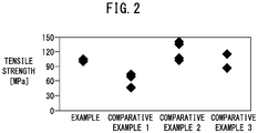
FIG. 2 is a graph showing magnitude of variation in tensile strength when the tensile test has been performed in an environment of -40°C using specimens of Example and Comparative Examples 1 to 3; and -
FIG. 3 is a graph showing magnitude of variation in tensile strength when the tensile test has been performed at from -40°C to over 100°C for Comparative Example 1. - A preferred embodiment of a solder material according to the present invention will be presented and described in detail below with reference to the accompanying drawings.
- A solder material according to the present embodiment is a so-called Pb-free solder material which is mainly composed of Sn and contains Ag and Cu to encourage precipitation strengthening, and to which In and Sb are further added. That is, this solder material is configured from an alloy that includes 2.5 to 3.3% (wt%, hereafter, the same) Ag, 0.3 to 0.5% Cu, 5.5 to 6.4% In, and 0.5 to 1.4% Sb, and whose remainder is unavoidable impurities and Sn.
- By setting Ag to 2.5% or more, precipitation strengthening is encouraged as described above. Now, when tensile strength obtained by performing a tensile test a plurality of times in an environment of -40°C on specimens of a Sn-Ag-Cu-In-Sb alloy in which Ag is 3.0% and 3.5% is plotted, variation in tensile strength is found to be larger when Ag is 3.5% compared to when it is 3.0%.
- The reason for this is inferred to be because when Ag is 3.5%, there is a eutectic composition of Sn-Ag, so there is a structure in which sub-eutectic substance, eutectic substance, and hyper-eutectic substance are mixed. Therefore, Ag is set to not more than 3.3% in order not to have a eutectic composition. As a result, it is avoided that sub-eutectic substance, eutectic substance, and hyper-eutectic substance are mixed in the structure, and variation in tensile strength can be suppressed.
- Cu of 0.3% or more also similarly results in precipitation strengthening being encouraged. On the other hand, when there is a eutectic composition of Sn-Cu, that is, when Cu is roughly 0.7%, it results in a structure in which sub-eutectic substance, eutectic substance, and hyper-eutectic substance are mixed, and variation in tensile strength ends up occurring. In order to avoid this, Cu is set to not more than 0.5%.
- Moreover, by adding 5.5% or more In, solid solution strengthening is promoted, and a melting point of the solder material lowers. That is, this solder material has a lower melting point compared to a Pb-free solder material containing only Sn, Ag, and Cu. Therefore, it melts at a low temperature when joining the electronic component to the circuit board, and so on.
- On the other hand, if an excess of In is added to Sn, a transformation point of the Sn lowers. For example, at 125°C or more, it transforms into y phase (InSn4). Such a second phase is part of the reason for variation occurring in mechanical characteristics of the solder material. Accordingly, in order to avoid this, In is set to not more than 6.4%. In this case, twinning deformation never occurs in the solder material.
- Furthermore, by adding 0.5% or more Sb, solid solution strengthening is promoted. Moreover, InSn4 and β-Sn are generated in a liquid phase along with In, whereby crystal grains become minute, thereby resulting in multiple crystal orientations. That is, the solder material shows almost no anisotropy. In other words, it is possible to come close to isotropy.
- When specimens configured from an alloy whose proportion of Sb to Sn has been set in a range of 1.0% to 3.0% are used, and stress-strain curves when a tensile test has been performed in an environment of -40°C are found, a result is obtained that although tensile strength increases as the proportion of Sb increases, variation in the tensile strength also increases as the proportion of Sb increases. Specifically, when the proportion of Sb to Sn has been set to 3.0%, a place where stress sharply falls and rises, that is, a disturbance is found to appear in the stress-strain curve. The reason for this is inferred to be that, due to a large amount of the solid solution element, slip deformation does not occur, and as a result, it becomes easier for twinning deformation to occur. In order to avoid this, Sb is set to not more than 1.4% at which twinning deformation does not readily occur.
- Moreover, when specimens configured from an alloy whose proportion of Bi to Sn has been set to 1.0%, 2.0%, and 3.0% are used, and stress-strain curves when a tensile test has been performed in an environment of -40°C are found, variation in tensile strength is found to increase even at 1.0%, and a disturbance is found to appear in the stress-strain curve even at 2.0%. The reason for this is thought to be that in the case of Bi having been added, twinning deformation occurs significantly more easily compared to in the case of Sn. Therefore, in the present embodiment, a substantive added amount of Bi is set to zero.
- A typical composition of a solder material is Sn-3.0Ag-0.5Cu-6.0In-1.0Sb. That is, the typically composed solder material contains 3.0% Ag, 0.5% Cu, 6.0% In, and 1.0% Sb, and its remainder is Sn and unavoidable impurities.
- By adopting such a composition, a solder material whose melting point is low and that has variation in tensile strength suppressed, is obtained. Hence, first, since low temperature melting and joining in reflow are enabled, thermal damage received by the electronic component when the electronic component is joined to the circuit board, for example, can be reduced.
- Moreover, since variation in tensile strength is small, life of the joined section that has been joined using the solder material becomes stable with little variation. Hence, reliability is improved. Moreover, since variation in product life of the joined article (for example, the on-board engine control unit, and so on) is suppressed, design flexibility of the joined article is improved, and a high-density or downsized product can be obtained.
- Specimens configured from the solder material (alloy) whose composition is Sn-3.0Ag-0.5Cu-6.0In-1.0Sb were prepared, and a tensile test was performed a plurality of times in an environment of -40°C, to find a stress-strain curve in each test. Hereafter, this specimen will also be called Example.
- Separately from this, specimens configured from solder materials of Comparative Examples 1-3 were prepared, and, similarly to as described above, a tensile test was performed a plurality of times in an environment of -40°C, to find a stress-strain curve in each test. Now, Comparative Example 1 includes neither In nor Sb at all, and Comparative Example 2 includes over 3.0% Ag and over 3.0% Bi. Moreover, Comparative Example 3 includes over 3.0% Ag, over 0.7% Cu, and over 0.7% Bi.
- Results of Example are shown in
FIG. 1 with a kind of line made different for each time. Furthermore, values of tensile strength in each of the specimens found from the stress-strain curves are shown inFIG. 2 as well. It may be understood from theseFIGS. 1 and2 that in Example, stresses in the respective tests substantially coincide (that is, variation in tensile strength is extremely small), whereas in Comparative Examples 1 to 3, stresses differ test by test, hence variation in tensile strength is large. That is, adopting the composition of Example results in a solder material having stable tensile strength (mechanical characteristics) being obtained. - Note that on comparing melting points of Example and Comparative Example 1, the melting point of Example was found to be approximately 20°C lower. This means that the solder material of Example melts more easily at a lower temperature compared to that of Comparative Example 1.
- Furthermore, in Comparative Example 2, it was confirmed that a large disturbance appeared in the stress-strain curve. As a result, in Comparative Example 2, variation in tensile strength is increased.
- Tensile strength was measured in a temperature range of from -40°C to over 100°C, for specimens of Comparative Example 1. Results are shown in
FIG. 3 . It may be understood from thisFIG. 3 that variation in tensile strength tends to increase as temperature lowers. - Crystal orientation analysis was performed and a Schmidt factor was calculated for a specimen whose tensile strength was 75 MPa and for a specimen whose tensile strength was 45MPa, of the specimens of Comparative Example 1 that had undergone the tensile test at -40°C. As a result, the Schmidt factor was 0.13 for the former and 0.47 for the latter. That is, the Schmidt factor of the specimen having the large tensile strength was small, and the Schmidt factor of the specimen having the small tensile strength was large. It is inferred from this correlation that a main cause of variation is due to there being anisotropy in the crystal orientation.
- Furthermore, when microscopic observation of structure was performed for the specimen of Comparative Example 2, it was confirmed that significant twinning deformation occurred in a specimen where the disturbance appearing in the stress-strain curve was large, whereas in a specimen where the disturbance was small, although twinning deformation did occur, a scale of that twinning deformation was small. That is, the larger the twinning deformation was, the larger the disturbance appearing in the stress-strain curve was, and the larger variation in the tensile strength was.
- In contrast, in Example, stable tensile strength was shown even in the environment of -40°C as described above, and furthermore, twinning deformation could not be found even when microscopic observation was performed. It is clear from this that setting the composition within the above-described range and substantively setting Bi to zero results in a solder material having a small variation in tensile strength being obtained.
Claims (4)
- A solder material including 2.5 to 3.3 wt% Ag, 0.3 to 0.5 wt% Cu, 5.5 to 6.4 wt% In, and 0.5 to 1.4 wt% Sb, a remainder thereof being unavoidable impurities and Sn.
- The solder material according to claim 1, wherein the solder material does not substantively include Bi.
- The solder material according to claim 1 or 2, wherein a crystal orientation thereof is isotropic.
- The solder material according to any one of claims 1 to 3, wherein the solder material does not include twinning deformation in its structure.
Applications Claiming Priority (2)
| Application Number | Priority Date | Filing Date | Title |
|---|---|---|---|
| JP2017076417A JP6397079B1 (en) | 2017-04-07 | 2017-04-07 | Solder material |
| PCT/JP2018/012113 WO2018186218A1 (en) | 2017-04-07 | 2018-03-26 | Solder material |
Publications (2)
| Publication Number | Publication Date |
|---|---|
| EP3608050A1 true EP3608050A1 (en) | 2020-02-12 |
| EP3608050A4 EP3608050A4 (en) | 2020-08-05 |
Family
ID=63668552
Family Applications (1)
| Application Number | Title | Priority Date | Filing Date |
|---|---|---|---|
| EP18781426.4A Withdrawn EP3608050A4 (en) | 2017-04-07 | 2018-03-26 | SOLDER MATERIAL |
Country Status (6)
| Country | Link |
|---|---|
| US (1) | US20210031310A1 (en) |
| EP (1) | EP3608050A4 (en) |
| JP (1) | JP6397079B1 (en) |
| CN (1) | CN110461534A (en) |
| BR (1) | BR112019020826A2 (en) |
| WO (1) | WO2018186218A1 (en) |
Families Citing this family (2)
| Publication number | Priority date | Publication date | Assignee | Title |
|---|---|---|---|---|
| JP2020049543A (en) * | 2018-09-28 | 2020-04-02 | 株式会社ケーヒン | Solder material |
| CN117139917B (en) * | 2023-10-31 | 2024-03-08 | 苏州塞一澳电气有限公司 | Lead-free solder for automobile glass and preparation method and application thereof |
Family Cites Families (13)
| Publication number | Priority date | Publication date | Assignee | Title |
|---|---|---|---|---|
| WO1997009455A1 (en) | 1995-09-01 | 1997-03-13 | Sarnoff Corporation | Soldering composition |
| US6176947B1 (en) * | 1998-12-31 | 2001-01-23 | H-Technologies Group, Incorporated | Lead-free solders |
| JP2002120085A (en) * | 2000-10-12 | 2002-04-23 | H Technol Group Inc | Lead-free solder alloy |
| HU228577B1 (en) * | 2000-11-16 | 2013-04-29 | Singapore Asahi Chemical And Solder Ind Pte Ltd | Lead-free solders |
| JP2004188453A (en) * | 2002-12-11 | 2004-07-08 | Harima Chem Inc | Sn-based solder alloy |
| CN1788918A (en) * | 2005-12-20 | 2006-06-21 | 徐振五 | Leadless environment-friendly soldering |
| DE102006047764A1 (en) * | 2006-10-06 | 2008-04-10 | W.C. Heraeus Gmbh | Lead-free soft solder with improved properties at temperatures> 150 ° C |
| WO2009011392A1 (en) * | 2007-07-18 | 2009-01-22 | Senju Metal Industry Co., Ltd. | In-containing lead-free solder for on-vehicle electronic circuit |
| US8598464B2 (en) * | 2009-04-20 | 2013-12-03 | Panasonic Corporation | Soldering material and electronic component assembly |
| US20140186208A1 (en) * | 2012-05-10 | 2014-07-03 | Senju Metal Industry Co., Ltd. | Audio solder alloy |
| WO2014013632A1 (en) * | 2012-07-19 | 2014-01-23 | ハリマ化成株式会社 | Solder alloy, solder paste, and electronic circuit board |
| JP6200534B2 (en) * | 2015-03-24 | 2017-09-20 | 株式会社タムラ製作所 | Lead-free solder alloy, electronic circuit board and electronic control device |
| WO2016185674A1 (en) * | 2015-05-19 | 2016-11-24 | パナソニックIpマネジメント株式会社 | Solder alloy and package structure using same |
-
2017
- 2017-04-07 JP JP2017076417A patent/JP6397079B1/en active Active
-
2018
- 2018-03-26 EP EP18781426.4A patent/EP3608050A4/en not_active Withdrawn
- 2018-03-26 CN CN201880021975.9A patent/CN110461534A/en active Pending
- 2018-03-26 US US16/500,171 patent/US20210031310A1/en not_active Abandoned
- 2018-03-26 BR BR112019020826-7A patent/BR112019020826A2/en not_active Application Discontinuation
- 2018-03-26 WO PCT/JP2018/012113 patent/WO2018186218A1/en not_active Ceased
Also Published As
| Publication number | Publication date |
|---|---|
| BR112019020826A2 (en) | 2020-05-12 |
| JP2018176191A (en) | 2018-11-15 |
| CN110461534A (en) | 2019-11-15 |
| US20210031310A1 (en) | 2021-02-04 |
| WO2018186218A1 (en) | 2018-10-11 |
| JP6397079B1 (en) | 2018-09-26 |
| EP3608050A4 (en) | 2020-08-05 |
Similar Documents
| Publication | Publication Date | Title |
|---|---|---|
| Xiao et al. | Aging and creep behavior of Sn3. 9Ag0. 6Cu solder alloy | |
| US10343238B2 (en) | Lead-free solder alloy | |
| US5455004A (en) | Lead-free alloy containing tin, zinc, indium and bismuth | |
| WO2007102588A1 (en) | Lead-free solder alloy, solder ball and electronic member, and lead-free solder alloy, solder ball and electronic member for automobile-mounted electronic member | |
| Zhang et al. | Intermetallic compound layer growth between SnAgCu solder and Cu substrate in electronic packaging | |
| Lai et al. | Interfacial microstructure evolution and shear strength of Sn0. 7Cu–x Ni/Cu solder joints | |
| US20210031310A1 (en) | Solder material | |
| US5718868A (en) | Lead-free tin-zinc-based soldering alloy | |
| EP3707285A1 (en) | Low-silver tin based alternative solder alloy to standard sac alloys for high reliability applications | |
| Marques et al. | Microstructural evolution at Cu/Sn–Ag–Cu/Cu and Cu/Sn–Ag–Cu/Ni–Au ball grid array interfaces during thermal ageing | |
| WO2009022758A1 (en) | Pb-free solder compositions and pcb and electronic device using the same | |
| EP1930117B1 (en) | Lead-free low-temperature solder | |
| KR20040063990A (en) | Lead-free soft solder | |
| US20240238914A1 (en) | Solder Alloy, Solder Paste, Solder Ball, Solder Preform, Solder Joint, Vehicle-Mounted Electronic Circuit, ECU Electronic Circuit, Vehicle-Mounted Electronic Circuit Device, and ECU Electronic Circuit Device | |
| US20240238912A1 (en) | Solder Alloy, Solder Paste, Solder Ball, Solder Preform, Solder Joint, Vehicle-Mounted Electronic Circuit, ECU Electronic Circuit, Vehicle-Mounted Electronic Circuit Device, and ECU Electronic Circuit Device | |
| Cai et al. | Mitigation of lead free solder aging effects using doped SAC-X alloys | |
| CN111230355B (en) | Lead-free solder alloy | |
| JP2001129682A (en) | Sn BASED Pb-FREE SOLDER SUPERIOR IN HEAT CYCLE CHARACTERISTICS | |
| EP3299113B1 (en) | Solder alloy and package structure using same | |
| Shohji et al. | Tensile properties of Sn-3.5 Ag and Sn-3.5 Ag-0.75 Cu lead-free solders | |
| Belyakov et al. | Role of Bi, Sb and In in microstructure formation and properties of Sn-0.7 Cu-0.05 Ni-X BGA interconnections | |
| Beáta et al. | Development of SnAgCu solders with Bi and In additions and microstructural characterization of joint interface | |
| CN115178910B (en) | Cost-effective lead-free solder alloy for electronic applications | |
| EP1103337A1 (en) | Tin-bismuth-based lead-free solder | |
| Oliver et al. | Fatigue properties of Sn/3.5 ag/0.7 cu solder joints and effects of Pb-contamination |
Legal Events
| Date | Code | Title | Description |
|---|---|---|---|
| STAA | Information on the status of an ep patent application or granted ep patent |
Free format text: STATUS: THE INTERNATIONAL PUBLICATION HAS BEEN MADE |
|
| PUAI | Public reference made under article 153(3) epc to a published international application that has entered the european phase |
Free format text: ORIGINAL CODE: 0009012 |
|
| STAA | Information on the status of an ep patent application or granted ep patent |
Free format text: STATUS: REQUEST FOR EXAMINATION WAS MADE |
|
| 17P | Request for examination filed |
Effective date: 20191104 |
|
| AK | Designated contracting states |
Kind code of ref document: A1 Designated state(s): AL AT BE BG CH CY CZ DE DK EE ES FI FR GB GR HR HU IE IS IT LI LT LU LV MC MK MT NL NO PL PT RO RS SE SI SK SM TR |
|
| AX | Request for extension of the european patent |
Extension state: BA ME |
|
| DAV | Request for validation of the european patent (deleted) | ||
| DAX | Request for extension of the european patent (deleted) | ||
| A4 | Supplementary search report drawn up and despatched |
Effective date: 20200702 |
|
| RIC1 | Information provided on ipc code assigned before grant |
Ipc: C22C 13/00 20060101ALI20200626BHEP Ipc: B23K 35/26 20060101AFI20200626BHEP |
|
| RAP1 | Party data changed (applicant data changed or rights of an application transferred) |
Owner name: HITACHI ASTEMO, LTD. |
|
| STAA | Information on the status of an ep patent application or granted ep patent |
Free format text: STATUS: THE APPLICATION HAS BEEN WITHDRAWN |
|
| 18W | Application withdrawn |
Effective date: 20220201 |