EP3607307B1 - Vorrichtung und verfahren zur erfassung von neuronalen aufzeichnungen - Google Patents
Vorrichtung und verfahren zur erfassung von neuronalen aufzeichnungen Download PDFInfo
- Publication number
- EP3607307B1 EP3607307B1 EP18781570.9A EP18781570A EP3607307B1 EP 3607307 B1 EP3607307 B1 EP 3607307B1 EP 18781570 A EP18781570 A EP 18781570A EP 3607307 B1 EP3607307 B1 EP 3607307B1
- Authority
- EP
- European Patent Office
- Prior art keywords
- micro
- electrode
- mea
- electrodes
- electrical
- Prior art date
- Legal status (The legal status is an assumption and is not a legal conclusion. Google has not performed a legal analysis and makes no representation as to the accuracy of the status listed.)
- Active
Links
Images


Classifications
-
- G—PHYSICS
- G01—MEASURING; TESTING
- G01N—INVESTIGATING OR ANALYSING MATERIALS BY DETERMINING THEIR CHEMICAL OR PHYSICAL PROPERTIES
- G01N33/00—Investigating or analysing materials by specific methods not covered by groups G01N1/00 - G01N31/00
- G01N33/48—Biological material, e.g. blood, urine; Haemocytometers
- G01N33/483—Physical analysis of biological material
- G01N33/4833—Physical analysis of biological material of solid biological material, e.g. tissue samples, cell cultures
- G01N33/4836—Physical analysis of biological material of solid biological material, e.g. tissue samples, cell cultures using multielectrode arrays
-
- A—HUMAN NECESSITIES
- A61—MEDICAL OR VETERINARY SCIENCE; HYGIENE
- A61B—DIAGNOSIS; SURGERY; IDENTIFICATION
- A61B5/00—Measuring for diagnostic purposes; Identification of persons
- A61B5/24—Detecting, measuring or recording bioelectric or biomagnetic signals of the body or parts thereof
- A61B5/25—Bioelectric electrodes therefor
- A61B5/279—Bioelectric electrodes therefor specially adapted for particular uses
- A61B5/291—Bioelectric electrodes therefor specially adapted for particular uses for electroencephalography [EEG]
- A61B5/293—Invasive
-
- A—HUMAN NECESSITIES
- A61—MEDICAL OR VETERINARY SCIENCE; HYGIENE
- A61B—DIAGNOSIS; SURGERY; IDENTIFICATION
- A61B5/00—Measuring for diagnostic purposes; Identification of persons
- A61B5/68—Arrangements of detecting, measuring or recording means, e.g. sensors, in relation to patient
- A61B5/6846—Arrangements of detecting, measuring or recording means, e.g. sensors, in relation to patient specially adapted to be brought in contact with an internal body part, i.e. invasive
- A61B5/6847—Arrangements of detecting, measuring or recording means, e.g. sensors, in relation to patient specially adapted to be brought in contact with an internal body part, i.e. invasive mounted on an invasive device
- A61B5/685—Microneedles
-
- G—PHYSICS
- G01—MEASURING; TESTING
- G01N—INVESTIGATING OR ANALYSING MATERIALS BY DETERMINING THEIR CHEMICAL OR PHYSICAL PROPERTIES
- G01N27/00—Investigating or analysing materials by the use of electric, electrochemical, or magnetic means
-
- A—HUMAN NECESSITIES
- A61—MEDICAL OR VETERINARY SCIENCE; HYGIENE
- A61B—DIAGNOSIS; SURGERY; IDENTIFICATION
- A61B2503/00—Evaluating a particular growth phase or type of persons or animals
- A61B2503/42—Evaluating a particular growth phase or type of persons or animals for laboratory research
-
- A—HUMAN NECESSITIES
- A61—MEDICAL OR VETERINARY SCIENCE; HYGIENE
- A61B—DIAGNOSIS; SURGERY; IDENTIFICATION
- A61B2562/00—Details of sensors; Constructional details of sensor housings or probes; Accessories for sensors
- A61B2562/02—Details of sensors specially adapted for in-vivo measurements
- A61B2562/0209—Special features of electrodes classified in A61B5/24, A61B5/25, A61B5/283, A61B5/291, A61B5/296, A61B5/053
-
- A—HUMAN NECESSITIES
- A61—MEDICAL OR VETERINARY SCIENCE; HYGIENE
- A61B—DIAGNOSIS; SURGERY; IDENTIFICATION
- A61B2562/00—Details of sensors; Constructional details of sensor housings or probes; Accessories for sensors
- A61B2562/02—Details of sensors specially adapted for in-vivo measurements
- A61B2562/028—Microscale sensors, e.g. electromechanical sensors [MEMS]
-
- A—HUMAN NECESSITIES
- A61—MEDICAL OR VETERINARY SCIENCE; HYGIENE
- A61B—DIAGNOSIS; SURGERY; IDENTIFICATION
- A61B2562/00—Details of sensors; Constructional details of sensor housings or probes; Accessories for sensors
- A61B2562/04—Arrangements of multiple sensors of the same type
- A61B2562/046—Arrangements of multiple sensors of the same type in a matrix array
Definitions
- the present disclosure relates to the field of micro-electrodes.
- the present disclosure relates to micro-electrodes and arrays thereof for detecting the electrical activity of an electrically-excitable cell or a network of electrically-excitable cells.
- ECNs excitable cellular-networks
- WO2015143443A1 relates to multi-site electrode arrays and methods of making the same.
- US20090283425A1 relates to a microelectrode array system with integrated reference microelectrodes to reduce detected electrical noise and improve selectivity of activation.
- planar-MEAs planar micro-electrodes that form part of planar micro-electrode arrays
- the planar-MEAs can interface with an ECN for studying homogeneous neuron populations within controlled extra-cellular environments. It is also known to interface hippocampal brain slices with planar-MEAs to study intact three-dimensional ECNs in an effort to mimic the scenario found in vivo. The preservation of ECNs is crucial when investigating neural function and, in particular, during attempts to perturb the connectivity within the ECN.
- the signal-to-noise ratio (SNR) within recordings captured by known MEAs, such as planar-MEAs, is often very low and this can interfere with the ability to conduct longer-term experimentation. Longer-term experimentation is desired for various investigations including but not limited to drug screening and in understanding the neural pathways and foci of electrical activity in the brain for various neurological diseases including but not limited to epilepsy. As shown in FIG. 1 , the limitations of known MEAs may be due to at least three factors:
- planar micro-electrodes or planar-MEAs may be questionable due to the viability of the neurons being recorded, which makes interpretation of that data difficult.
- Embodiments of the present disclosure relate to a three-dimensional (3D) micro-electrode comprising an electrically conductive, elongate body with: a base that is electrically connectible to a recording system; a tip that is opposite the base and that is configured to establish electrical communication with an excitable cellular-network (ECN); and an elongate portion between the base and the tip.
- the elongate portion is optionally covered with at least one layer of an electrical-insulator coating that extends from the base to proximal the tip.
- the 3D-microelectrode is configured to come into contact with or penetrate at least partially into a subject's tissue (either in vitro, ex vivo or in vivo ) so that the tip is in electrical communication with the one or more cells of the ECN.
- the electrical-insulator coating may reduce the signal artifact that may arise from passing through the outer layer of the subject's tissue.
- micro-electrode array that comprises at least two 3D micro-electrodes, as described above, which are electrically connectible to at least one recording system.
- the 3D-MEA can be used to present the tips of multiple 3D micro-electrodes into electrical communication with one or more cells of an ECN.
- Each 3D-microelectrodes of the 3D-MEA can be selectively fabricated so that all 3D micro-electrodes have substantially the same dimensions of height and diameter or not.
- each 3D micro-electrode can be selected during the fabrication process so that the 3D-MEA is optimally designed for a given in vitro, ex vivo or in vivo application.
- 3D micro-electrodes that are positioned within a specific region of the 3D-MEA may be longer to reach further into a specific region of the subject's tissue preparation.
- Other 3D micro-electrodes that are positioned within a specific region of the 3D-MEA may have a larger diameter in order to establish more robust electrical communication with a specific region of the subject's tissue preparation.
- inventions of the present disclosure relate to a method of fabricating 3D micro-electrodes and 3D-MEAs to create a multisite recording platform that permits in vitro, ex vivo and in vivo high-resolution, long-term recording of electrical activity of ECNs with higher signal-to-noise ratio and that cause less tissue damage than known devices.
- Each 3D micro-electrode that is part of a 3D-MEA can be selectively fabricated so that the dimensions of height and diameter are selected based upon the region of the subject's tissue preparation those 3D micro-electrodes are intended to establish electrical communication with.
- the amount of the tip of each 3D micro-electrode that is bare and not coated in the electrical-insulator coating can be selected as well.
- the shape of the tip of each 3D micro-electrode may also be selectively fabricated between blunt, sharp or flat. The shape of the tip may be selected based upon the region of the subject's tissue preparation that the 3D micro-electrode is intended to establish electrical communication with.
- FIG. 1 A block diagram illustrating an exemplary computing environment in accordance with the present disclosure.
- FIG. 1 A block diagram illustrating an exemplary computing environment in accordance with the present disclosure.
- FIG. 1 A block diagram illustrating an exemplary computing environment in accordance with the present disclosure.
- FIG. 1 A block diagram illustrating an exemplary computing environment in accordance with the present disclosure.
- FIG. 1 A block diagram illustrating an exemplary computing environment in accordance with the present disclosure.
- planar micro-electrodes and planar micro-electrode arrays can only record neural activity from the external layer of tissue that contains electrically-excitable cells.
- the selectable length of the 3D micro-electrodes and 3D-MEAs of the present disclosure may allow the 3D micro-electrode tip to access more deeply within the subject's tissue preparation and, therefore, establish electrical communication with undamaged cells.
- the electrically-insulated elongate portions and bases of the 3D micro-electrodes of the present disclosure may decrease the recorded noise from ionic movement within the local environment while providing structural support.
- embodiments of the present disclosure may be useful for increasing the understanding and potential treatment of neuro-degenerative diseases such as, but not limited to: Alzheimer, Parkinson and epilepsy.
- the present disclosure may also be useful for increasing understanding of cognitive, emotional and behavioral abilities within a subject.
- Embodiments of the present disclosure may also be useful for controlling neuro-prosthetics, providing feedback to the patients and allow for development of personalized medication or therapies for neuro-degenerative diseases.
- Using embodiments of the present disclosure for research may also be useful for drug screening as well as understanding fundamental brain functions including, but not limited to, neural network phenomena.
- the term "about” refers to an approximately +/-10% variation from a given value. It is to be understood that such a variation is always included in any given value provided herein, whether or not it is specifically referred to.
- the term "electrical communication" refers to a one-way flow of an electrical signal and/or a two-way exchange of electrical signals.
- the one-way flow of the electrical signal may originate in: at least one electrically-excitable cell, a three-dimensional (3D) micro-electrode according to the present disclosure or both.
- the two-way exchange of electrical signals refers to both the transmission and receipt of electrical signals by a 3D micro-electrode and at least one electrically-excitable cell.
- Electrical communication may also refer to the detection and/or transmission of an electrical signal between the 3D micro-electrode and at least one electrically-excitable cell.
- electrically-excitable cell refers to a cell that have the potential to communicate charged ions across the cellular membrane in response to an electric, chemical or physical stimuli.
- the electrically-excitable cells can depolarize in a regulated fashion to generate and propagate one or more action potentials or end-plate potentials.
- electrically-excitable cells include but are not limited to all types of neural cells and muscle cells.
- excitable cellular-network and the acronym “ECN” refer to a network of electrically-excitable cells that are interconnected so that stimulation of one or more than one electrically-excitable cell within the network will elicit a response in at least one other electrically-excitable cell within the network.
- the response of at least one other electrically-excitable cell will include a communication of charged ions across its cellular membrane and/or the release of one or more extra-cellular signal molecules.
- tissue preparation refers to a subject's tissue that comprises one or more electrically excitable cells and at least a portion of an ECN.
- a 3D-MEA according to the present disclosure can come into contact with a tissue preparation and establish in vitro, ex vivo or in vivo electrical communication with the one or more electrically excitable cells and at least a portion of the ECN.
- the present disclosure relates to a 3D micro-electrode 210 for establishing electrical communication with a single electrically-excitable cell and/or a network of electrically-excitable cells, which is referred to herein as an excitable cellular-network (ECN) (see FIG. 1 (B) ).
- the 3D micro-electrode 210 comprises an electrically conductive, elongate body 204 with a base 202 that is electrically connectible to a recording system.
- the 3D micro-electrode 210 also comprises a tip 206 that is opposite the base 202 and that is configured to establish electrical communication with at least a portion of an ECN.
- the elongate portion 204 is defined between the base 202 and the tip 206.
- the base 202 typically has a larger diameter than the elongate portion 204 and the elongate portion typically has a greater length than the base 202 and the tip 206.
- the tip 206 is frustoconical in shape with a decreasing diameter to a fine point with a diameter that is many times less than the diameter of the elongate portion 204.
- a substrate 102 can comprise multiple layers (e.g. the additional materials 104 placed in between the substrate 102 and an electrically conductive, electrode supporting pad 109) that support each 3D-microelectrode 210. Some of these multiple layers, or portions of which, may be removed or degraded during the fabrication process.
- the additional material 104 can be placed on the substrate 102 that provides structural support for one or more layers of different materials thereupon (e.g. the layer of conductive material that forms the pads 109).
- the substrate 102 is rigid and in some instances the substrate 102 is more flexible.
- the further layers of materials upon the substrate 102 may be provided to allow different materials (e.g. the different materials that make up the pads 109 and the wires 105) to be attached to the substrate 102.
- the elongate portion 204 may be covered with at least one layer of an electrical-insulator coating 208 that extends from the base 202 towards and proximal the tip 206.
- the tip 206 of the 3D micro-electrode 210 is configured to establish electrical communication with the ECN.
- the 3D micro-electrode 210 may establish electrical communication with the ECN by direct physical contact, or not.
- the 3D micro-electrodes 210 are configured to penetrate at least partially into a tissue preparation 12 (shown in FIG. 2H ) that comprises electrically-excitable cells and that make up at least a portion of the ECN.
- At least two 3D micro-electrodes 210 are configured into an array, referred to herein as a 3D micro-electrode array (3D-MEA) 212 (shown in FIG. 1(B) ).
- the 3D-MEA 212 can be used with various types of tissue preparations 12 including, but not limited to: in vitro tissue preparations 12, ex vivo tissue preparations 12 or in vivo tissue preparations 12.
- the 3D-MEA 212 can be used to establish electrical communication with the ECN within the tissue preparation 12 for detecting any changes in the electrical activity of the ECN in response to electrical stimuli, chemical stimuli or physical stimuli.
- the 3D-MEA 212 can establish electrical communication for stimulating the ECN within the tissue preparation 12. In some embodiments of the present disclosure, the 3D-MEA 212 can establish electrical communication for both detecting and stimulating the ECN within the tissue preparation 12.
- the two 3D micro-electrodes 210 of the 3D-MEA 212 are electrically connectible to the same recording system. As shown in FIG. 1(B) , an individual 3D-MEA 212 may comprise 3D micro-electrodes 210 that have different lengths and/or different diameters.
- each individual 3D micro-electrode 210 of a given 3D-MEA 212 can be selectively fabricated based upon the method described herein and the specific dimensions of each 3D micro-electrode 210 can be individually selected based upon the desired application of use of the 3D-MEA 212.
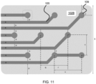
- FIG. 10 shows one embodiment of a 3D-MEA 212 that comprises the substrate 102 with a first substrate portion 104A and a second substrate portion 104B.
- FIG. 10 , FIG. 11 and FIG. 12 (A) show planar portions of the 3D-MEA 212.
- the first substrate portion 104A includes one or more terminals 107 that are configured to provide electronic communication with a transmitter/receiver system (not shown). Extending from each terminal 107 is a wire section 105. The wire section extends from the first portion 104A to the second portion 104B and to the pads 109, which are located in the second portion 104B.
- the wire sections 105 are electrically conductive and provide electronic communication between each 3D micro-electrode 210 upon a given pad 109 and a given terminal 107.
- the wire sections 105 can be insulated or not, with one or more insulation layers.
- Each pad 109 is the location of the 3D-MEA 212 where the base 202 of a 3D micro-electrode 210 is deposited and attached to the substrate 102.
- FIG. 14 shows a photograph of two examples of a 3D-MEA 212 with one being in a flexed position between the pads 109 and the first substrate portion 104A.
- neither portion 104A, 104B is flexible. In some embodiments of the present disclosure, one of or both of the first portion 104A and the second portion 104B are flexible. As will be appreciated by one skilled in the art, having at least one portion of the substrate 102 being flexible is advantageous for establishing optimal physical contact or proximity between the 3D micro-electrodes 210 of a 3D-MEA 212 and the ECN that is defined by an oftentimes, non-flat, flexible surface of the tissue preparation 12.
- the design of the 3D-MEA 212 can be selected based upon the nature of the tissue preparation 12 that contains the ECN that the 3D-MEA 212 is intended to electrically communicate with.
- the substrate 102 may have a general T shape, or it may take any other desired shape.
- the first portion 104A and the second portion 104B each define various dimensions that are set out in Table 1 below. The person skilled in the art will appreciate that the dimensions provided in Table 1 are provided as examples only. The dimensions provided in Table 1 were selected based upon the intent of using the 3D-MEA 212 for establishing in vitro electrical communication with a rat brain tissue preparation.
- the 3D-MEA 212 can be selectively fabricated with larger or smaller dimensions than those presented in Table 1 below.
- a 3D-MEA 212 that is intended to be used with a human subject may be selectively fabricated with larger dimensions than those below in Table 1.
- Table 1 Examples of dimensions (mm, unless otherwise indicated) of a 3D-MEA according to one embodiment of the present disclosure.
- the 3D-MEA 212 can be manufactured on to a flexible and biocompatible substrate 102 that is configured to be implanted into a living organism.
- the 3D-MEA 212 can also be configured to detect the electrical activity of the in vivo ECN and/or to stimulate the in vivo ECN or specific regions thereof.
- Some embodiments of the present disclosure relate to a fabrication method of making a 3D micro-electrode 210 and a method of making a 3D-MEA 212.
- the 3D micro-electrodes 210 can be made individually with precise control of: the height and diameter of each 3D micro-electrode 210 within the 3D-MEA 212; the length of the elongate portion 204 that is covered in the electrical-insulator material 208; the length of the tip 206; and the shape of the tip 206.
- the fabrication method allows the selectability of the materials used to make the 3D micro-electrodes 210, the electrical insulating coatings 208 and the materials of each layer of the substrate 102 upon which the 3D-MEA 212 is built.
- the fabrication method also allows for selectability of the surface area of each 3D micro-electrode 210 that is not covered by the electrical insulating coating 208 and the position of these uncovered sections within the 3D-MEA 212.
- the fabrication method comprises a step to establish 300 a first layer comprised of one or more materials 104 and conductive materials that form the electrically conductive, electrode supporting pads 109 upon the substrate 102.
- the product of this first step is referred to as a coated blank 100.
- the next step of the fabrication method is to establish 302 one or more grooves 106 upon the coated blank 100 by removing one or more layers of the substrate 102.
- the next step of the fabrication step is to position 304 an electrical-insulating material 108 between the grooves to define one or more pads 109.
- the electrical-insulating material 108 can be deposited upon the substrate 102 and then substantially removed from the location of the pads 109.
- a layer of the electrical-insulating material 108 can have holes defined therein, and then that insulating layer can be adhered to the substrate 102 with pads 109 already thereupon. The holes in the insulating layer will align with the pads 109.
- the electrical-insulator material 108 can cover, or overlap, the peripheral edges of the pad 109. This overlap provides some additional rigid support while depositing the 3D micro-electrode 210 upon the pad 109.
- the next step in the fabrication method is to deposit 306 a conductive material upon the one or more pads 109.
- the step of depositing 306 can occur by various methods, including but not limited to: wire bonding (according to the invention), sputtering, electrodeposition, evaporation, extrusion, combinations thereof or other methods to make a conductive material of a desired geometry.
- the step of depositing 306 may further include a step of selecting the diameter of the elongate portion 204 of the 3D micro-electrode 210.
- each elongate portion 204 may be selected within a range of between about 1 microns and 1000 microns. In some embodiments of the present disclosure, the diameter of the elongate portion 204 may be selected to be within a range of between about 5 microns and about 750 microns. In some embodiments of the present disclosure, the diameter of the elongate portion 204 is between about 5 and 1000 microns.
- the step of depositing 306 includes forming the base 202 and a step of selecting the height of the 3D micro-electrode 210.
- the selecting of the length can include a step of stopping the depositing 306 of the conductive material upon the pad 109 and/or cutting the conductive material as it is being deposited. According to the invention, the length of the 3D micro-electrode 210 is selected by cutting the conductive material.
- Some of the methods of cutting the conductive material include, but are not limited to: using micro-scissors, electronic flame off (EFO) - whereby the conductive material is heated at a very localized position such that it melts and cuts the conductive material, use of a laser to cut the wire at a selected height, physically pulling the wire until it stretches and then breaks due to mechanical stresses, or combinations thereof.
- EFO electronic flame off
- the length of each elongate portion 204 may be selected within a range of between about 1 micron and 10 cm. In some embodiments of the present disclosure the length of each elongate portion 204 may be selected within a range of between about 1 micron and 5 cm.
- the length of the elongate portion 204 may be selected to be within a range of between about 5 microns and about 1000 microns. In some embodiments of the present disclosure, the length of the elongate portion 204 is between about 25 and 500 microns.
- the end of 3D micro-electrode 210 that is opposite to the base 202 is referred to as the tip 206.
- the elongate portion 204 of the 3D micro-electrode 210 is defined between the base 202 and the tip 206.
- the tip 206 is the portion of the elongate portion 204 that is not coated with the electrical-insulating coating 108.
- the method of selecting the height of the 3D micro-electrode 210 may also include providing the tip 206 with either a sharp, a blunt or a flat shape.
- the steps 302 to 306 can be repeated 308 to selectably fabricate the desired number of electrodes 210 in multiple locations on the substrate with the same or different diameters and lengths.
- the next step is to coat 310 the electrodes 210 with the electrical-insulating coating 108.
- the insulating materials may have other desirable properties such as, but not limited to, being curable, photoresistant, waterproof, biocompatible or combinations thereof.
- suitable materials for the electrical-insulating coating 108 includes, but is not limited to, dielectric and insulator materials, such as photoresists (both positive and negative), polymers, oxides, nitrides and ceramics.
- the material SU8 was utilized.
- SU8 is a chemically amplified, epoxy based negative photoresist that is optically transparent and photoimageable to near ultraviolet (UV) (about 365 nm) radiation.
- UV near ultraviolet
- Cured films or microstructures of SU8 are very resistant to solvents, acids and bases, have excellent thermal and mechanical stability and are biocompatible when cured.
- the coating step 310 can be achieved by various methods including, but not limited to: sputtering, spin coating, evaporation, casting, pouring, syringe dispensation, micropipette dispensation, combinations thereof or other methods that are commonly known to one skilled in the art.
- the fabrication method also includes a step of selecting 312 how much surface area and/or which portion(s) of the 3D micro-electrode 210 are coated with the insulating material. As shown in FIG. 2 (G) the step of selecting can result in some, most or all of the elongate portion 204 being coated in the insulating material. In some embodiments of the present disclosure, some, most, all or none of the tip 206 is coated in the insulating material. In some preferred embodiments, none of the tip 206 is coated in the insulating material.
- the detection method may comprise a step 314 of positioning the tips 206 of each 3D micro-electrode 210 within a tissue preparation 12 that comprises at least a portion of an ECN.
- the tissue preparation 12 may be an in vitro preparation, an ex vivo preparation or an in vivo preparation.
- the step 314 positioning includes positioning the 3D-MEA 212 proximal to an ECN and then establishing electrical communication between one or more 3D micro-electrodes 210 of the 3D-MEA 212 and the ECN.
- the step of establishing electrical communication may include receiving (also referred to as detecting) electrical signals from the ECN and/or transmitting electrical signals from the 3D-MEA 212 to the ECN.
- the detection method may further comprise a step of stimulating the ECN and detecting any changes in the electrical activity of the ECN.
- the ECN can be stimulated electrically (via the 3D-MEA 212 or not), mechanically or chemically.
- the electrical communication is transmitted from each electrode to a transmitter / receiver system (not shown).
- the transmitter / receiver system may transmit an output signal from each 3D micro-electrode 210 to a processor (not shown) for example when the 3D-MEA 212 is receiving electrical signals from the ECN.
- the transmitter may also transmit a processor signal to each 3D micro-electrode 210, which each electrode transmits to the ECN.
- Planar electrodes in 8 x 8 array configuration were fabricated using photolithography onto a substrate that had a rigid glass, base substrate layer and that measured 49 mm x 49 mm x 1 mm.
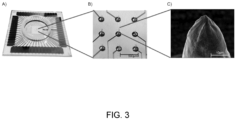
- the substrate included a 50 nm chrome adhesion layer that was coated by sputter deposition and the adhesion layer was then coated with about 400 nm of gold ( FIG. 2A ).
- the size, shape and the spacing between the planar micro-electrodes can be adjusted according to experimental needs using different photomasks during the photolithography process.
- the planar micro-electrodes were fabricated with a diameter of about 100 ⁇ m and with inter-electrode spacing of about 500 ⁇ m ( FIG. 2B ).
- a first electrical-insulator layer was formed with an epoxy photoresistant material (SU8), which was spin coated over the entire 3D-MEA.
- the insulator layer was then patterned with a second photomask to leave the planar electrodes bare of SU8 insulator, but with their connecting wires insulated ( FIG. 2C ). This formed the pads of the 3D-MEA.
- SU8 epoxy photoresistant material
- 3D micro-electrodes with a base, an opposite tapered tip and an elongate portion therebetween were added onto the pads of the planar electrodes using a manually programmable wire bonder (West-Bond model 454647E). Briefly, the 3D micro-electrodes were created by bonding gold wires onto the planar electrodes at the base of the 3D micro-electrode, manually extending the gold to a predetermined height and then cutting the gold wires with micro-scissors mounted on micro-manipulators ( FIG. 2D and FIG. 2E ). This cutting step formed a tip of the 3D micro-electrode that can be tapered, beveled, blunt or substantially flat.
- This method yields control and flexibility in the diameter and the height of each 3D micro-electrode and the inter-electrode spacing.
- Electrically conductive materials other than gold may also suitable for making the 3D micro-electrodes including but not limited to: aluminum, aluminum alloys such as. 0.5-1% magnesium-aluminum or silicon-aluminum, carbon, iridium, indium, titanium, copper, silver, palladium, platinum and combinations thereof and any other material that can be used in or adapted for any process to create 3D micro-electrodes, including at least a wire-bond process.
- the micro-electrodes can also be individually fabricated and addressable.
- the 3D gold micro-electrodes were fabricated with controlled heights ranging from about 50 microns ( ⁇ m) to about 400 ⁇ m with a diameter of between about 8 ⁇ m to about 500 ⁇ m depending on the bonder wires used.
- smaller or larger heights and diameters of 3D micro-electrodes are also contemplated by the present disclosure. These heights, spacing and materials were chosen specifically for recording from a 400 ⁇ m thick murine brain-slice but the 3D micro-electrode height and diameter and the 3D-MEA inter-electrode spacing may be adjusted individually, either increased or decreased, to suit other types of ECNs or different experimental arrangements with similar or different ECNs.
- a second electrical-insulator layer may be made up of the epoxy photoresist SU8 that was locally deposited on the bases and edges of the newly formed 3D micro-electrodes using a fine sharp glass micropipette with a 30 ⁇ m tip opening whose positioning was accurately controlled using a 3-axis micromanipulator ( FIG. 2F and FIG. 2G ).
- This micropipette was connected through a plastic tube to a syringe containing the SU8, which was itself mounted on a syringe micro-pump to control the flow (Harvard Apparatus Co., Dover, MA, USA, Dual infusion/withdrawal pump model 942).
- the SU8 was then cured with UV light to form the second electrical-insulator layer upon the 3D micro-electrodes.
- This process allowed the 3D-micro-electrode tips to be left without any of the second electrical-insulator layer for the last few micrometers so that the tip could establish electrical communication by direct contact with the healthy neural cells inside the brain slice ( FIG. 2 ).
- the amount of surface area of the tip that can come into direct contact with the neural cells can be adjusted by adding more or less of the second electrical-insulator layer on the 3D micro-electrodes of the 3D-MEA.
- a glass ring was then placed on the 3D-MEA to form a recording chamber ( FIG. 3A ).
- the small dark circles are the bases the 3D micro-electrodes, and the dark lines extending therefrom are the electrodes traces that connect each 3D micro-electrodes to the recording system on the outside of the 49 mm x 49 mm glass substrate.
- the recording chamber was perfused with either one of three types of artificial cerebrospinal fluid (aCSF): (1) "normal” aCSF; (2) “low” aCSF with 0 mM of Mg 2+ ; and (3) "high” aCSF with 8.5 mM of K + . All of the aCSF were used at about 32 °C, with about 5% CO 2 and about 95% O 2 .
- the different ion concentrations in the aCSF types (2) "low” and (3) "high” can cause spontaneous neural-activity to occur within the murine brain slices and are known to induce spontaneous seizure-like activity within murine brain slices.
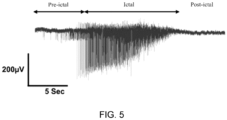
- Spontaneous, seizure-like activity is referred to herein as an ictal phase.
- a recording system (MEA1060; Multichannel Systems, Reutlingen, Germany) was then electrically connected with each 3D micro-electrode of the 3D-MEA to collect data at a 10 kHz sampling rate ( FIG. 5 and FIG. 6 ).
- the 3D micro-electrodes and the 3D-MEAs of the present disclosure may offer opportunities to track high frequency bursting activity between different areas of a brain slice and analyze its overall excitability.
- the SNR of the 3D micro-electrodes was then compared with earlier reported devices, including other three-dimensional (e.g. pyramidal-shaped) and planar micro-electrodes.
- the 3D micro-electrodes of the present disclosure demonstrated an average noise reduction to about 20 ⁇ V as compared to about 40 ⁇ V to about 60 ⁇ V observed in traditional planar micro-electrodes.
- the 3D micro-electrodes provided a highest recorded field potential activity peak-to-peak, which was in the mV range (about 3.2 mV) as compared with recordings of ⁇ 1 mV that were captured with traditional planar micro-electrodes ( FIG. 6 ).
- the 3D micro-electrodes and the 3D-MEAs of the present disclosure may offer a higher signal-to-noise ratio (with a greater than 300% improvement) than commercially available devices using traditional planar micro-electrodes.
- a temporal resolution may refer to either the time length of a given recording or the frequency of the recording, i.e. how many data points are recorded per second. In the present disclosure, the maximum time length of recording was about 3 hours and frequency of the recording can go up to about 50 kHz. It is also worth highlighting that the cured SU8 (the electrical-insulator layer) on the electrodes' edges provides structural support and reduces the physical degradation of the three-dimensional electrodes, thus allowing the MEAs to be re-used multiple times.
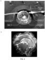
- FIG. 7 shows a picture taken with an optical microscope of an acute hippocampal brain slice positioned on an array of electrodes. Areas such as the mid-brain (MD), thalamus (TH) and hippocampus (H) are clearly visible.
- FIG. 8 shows the spontaneous electrical activity that was recorded using an embodiment of the present disclosure from sub-areas of the TH, including T1 to T7, whose positions are indicated on FIG. 7 .
- FIG. 9 shows the spontaneous electrical activity that was recorded using an embodiment of the present disclosure from sub-areas of the H, including H1 to H5, whose positioned are indicated on FIG. 7 .
- a similar method to the one described above for fabricating the in-vitro 3D-MEA was used to manufacture an implantable, and optionally flexible, 3D-MEA that can record activity from electrically excitable cells in vivo.
- the primary difference between the fabrication method described herein above for making the in vitro 3D-MEA and the in vivo 3D-MEA of the present example is that the planar electrodes were fabricated on a flexible substrate.
- the method steps for making the 3D micro-electrodes includes the same steps as described above.
- Various materials can be used for the substrate, the wires, the electrodes, and the electrical-insulator layer.
- the patterning of the wires and the electrodes can be performed in multiple ways.
- low impedance and high conductivity materials are preferred for making the wires and the electrodes.
- a flexible printed circuit board (flex PCB) was used as the substrate.
- the wires were made of copper using copper electrode traces subsequently coated by an Electroless Nickel Immersion Gold (ENIG) process to create wires and biocompatible electrode pads upon the flex PCB.
- ENIG Electroless Nickel Immersion Gold
- the 3D micro-electrodes were then fabricated on top of the electrode pads and their bases and edges were insulated by coating with the electrical-insulating material that is biocompatible.
- insulating material is SU8, but other insulating and biocompatible materials are known to those skilled in the art.
- the materials for fabricating the electrodes were selected from low impedance, high conductivity and magnetic resonance imaging (MRI) benign materials, for example gold, platinum and other known materials.
- MRI magnetic resonance imaging
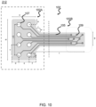
- FIG. 10 which shows a top plan view of a schematic of one example of the in vivo 3D-MEA without the 3D micro-electrodes manufactured upon the pads 109.
- the in vivo 3D-MEA had the following dimensions, which are provided as an example only and not as a limitation upon the embodiments of the present disclosure: a - 3 mm, b - 5.04 mm, c - 1.27 mm, c1 - 3.81 mm, d and f - 0.865 mm, e - 1.27 mm, g - 0.5 mm, h - 0.651 mm, j and k - 0.5 mm, 1 - 8 mm, m - 1.75 mm, n and o - 75 micron, q and r - 350 micron, s - 700 micron, t - 525 micron, u and v - 200 micron, w - 100 micron, x -
- the in vivo MEA flex PCB was held in place by a dental surgical acrylic and the scalp was held in place after implantation by the same acrylic.
- brain activity including ictal phases, were successfully recorded during more than 15 different experiments (100% success rate). Ictal phases were experimentally induced by kindling.
- the electrophysiological data collected in-vivo from the rat brains was transferred wirelessly to a computer to further the analysis of the electrophysiological activity.
- the data was also recorded locally onto a removable storage device, allowing for data to be backed up, and also available for later transfer. Ensuring fidelity of both recorded and transmitted data was important.
- the wireless data was also transmitted using compression techniques to allow live viewing of the
- FIG. 13 shows an example of baseline activity obtained from a live animal brain using a known MEA that did not have any electrical-insulating coating 108 and that had much larger dimensions than the in-vivo 3D-MEA.
- FIG. 13B shows an example of baseline activity obtained from a live animal brain using the in-vivo 3D-MEA. The decreased noise level from the signal obtained by the in-vivo 3D-MEA is apparent when comparing the two examples.
- FIG. 13C shows an example of electrical communication data obtained from a live rat brain that underwent an experimentally induced ictal phase (seizure), which was followed by a post-ictal period. The ictal phase is associated with an increased electrical activity, as evidenced by at least a ten-fold increase in detected voltage ( FIG. 13B shows increments of 0.2 V on the Y axis and FIG. 13C show increments of 2 V).
- the 3D micro-electrodes and 3D-MEAs described herein can be used to record activity from electrically excitable cells (Central Nervous System and Peripheral Nervous System, heart, muscle and others) and stimulate these cells using electrical stimulation. By establishing two-way electrical communication (both recording and stimulation), a feedback loop system can be established.
Landscapes
- Health & Medical Sciences (AREA)
- Life Sciences & Earth Sciences (AREA)
- Engineering & Computer Science (AREA)
- Physics & Mathematics (AREA)
- Biomedical Technology (AREA)
- Pathology (AREA)
- General Health & Medical Sciences (AREA)
- Biophysics (AREA)
- Molecular Biology (AREA)
- Chemical & Material Sciences (AREA)
- Animal Behavior & Ethology (AREA)
- Medical Informatics (AREA)
- Surgery (AREA)
- Veterinary Medicine (AREA)
- Heart & Thoracic Surgery (AREA)
- Public Health (AREA)
- Biochemistry (AREA)
- Immunology (AREA)
- General Physics & Mathematics (AREA)
- Analytical Chemistry (AREA)
- Hematology (AREA)
- Urology & Nephrology (AREA)
- Food Science & Technology (AREA)
- Medicinal Chemistry (AREA)
- Optics & Photonics (AREA)
- Electrochemistry (AREA)
- Chemical Kinetics & Catalysis (AREA)
- Measurement And Recording Of Electrical Phenomena And Electrical Characteristics Of The Living Body (AREA)
Claims (8)
- Verfahren zum Fertigen eines dreidimensionalen (3D-)Mikroelektrodenarrays (212), 3DMEA, wobei das Verfahren die folgenden Schritte umfasst:(a) Bilden von zwei oder mehr elektrisch leitenden Pads (109), die durch elektrisch isolierendes Material getrennt sind, auf einem flexiblen oder starren Substrat (102);(b) Drahtbonden eines Drahts an einem der zwei oder mehr elektrisch leitenden Pads (109), um einen länglichen Abschnitt (204) einer 3D-Mikroelektrode zu bilden;(c) Auswählen einer Höhe der 3D-Mikroelektrode und Schneiden des Drahts entsprechend der Höhe, wodurch eine Spitze (206) der 3D-Mikroelektrode distal zu dem Substrat (102) gebildet wird; und(d) Beschichten der 3D-Mikroelektrode (210) mit einer elektrisch isolierenden Schicht ohne Beschichten der Spitze (206).
- Verfahren nach Anspruch 1, ferner umfassend Auswählen eines Durchmessers des länglichen Abschnitts (204) der 3D-Mikroelektrode.
- Verfahren nach Anspruch 1, wobei der Schritt des Auswählens der Höhe der 3D-Mikroelektrode (210) zu einer ersten Höhe der 3D-Mikroelektrode auf einem ersten Pad und einer zweiten Höhe einer anderen 3D-Mikroelektrode auf einem zweiten Pad führt und wobei die zwei oder mehr elektrisch leitenden Pads das erste Pad und das zweite Pad umfassen.
- Verfahren nach Anspruch 3, wobei sich die erste Höhe und die zweite Höhe unterscheiden.
- Verfahren nach Anspruch 2, wobei der Schritt des Auswählens des Durchmessers des länglichen Abschnitts der 3D-Mikroelektrode (210) zu einem ersten Durchmesser eines länglichen Abschnitts der 3D-Mikroelektrode auf einem ersten Pad und einem zweiten Durchmesser eines anderen länglichen Abschnitts einer anderen 3D-Mikroelektrode (210) auf einem zweiten Pad (109) führt und wobei die zwei oder mehr elektrisch leitenden Pads das erste Pad und das zweite Pad umfassen.
- Verfahren nach Anspruch 5, wobei sich der erste Durchmesser und der zweite Durchmesser unterscheiden.
- Verfahren nach Anspruch 1, wobei die zwei oder mehr elektrisch leitenden Pads (109) zwischen einer oder mehreren Schichten des elektrisch isolierenden Materials definiert sind.
- Verfahren nach Anspruch 5, wobei der erste Durchmesser und der zweite Durchmesser im Wesentlichen gleich sind.
Applications Claiming Priority (2)
| Application Number | Priority Date | Filing Date | Title |
|---|---|---|---|
| US201762481473P | 2017-04-04 | 2017-04-04 | |
| PCT/CA2018/050411 WO2018184104A1 (en) | 2017-04-04 | 2018-04-04 | Apparatus and method for capturing neural recordings |
Publications (4)
| Publication Number | Publication Date |
|---|---|
| EP3607307A1 EP3607307A1 (de) | 2020-02-12 |
| EP3607307A4 EP3607307A4 (de) | 2020-09-16 |
| EP3607307C0 EP3607307C0 (de) | 2025-06-18 |
| EP3607307B1 true EP3607307B1 (de) | 2025-06-18 |
Family
ID=63712030
Family Applications (1)
| Application Number | Title | Priority Date | Filing Date |
|---|---|---|---|
| EP18781570.9A Active EP3607307B1 (de) | 2017-04-04 | 2018-04-04 | Vorrichtung und verfahren zur erfassung von neuronalen aufzeichnungen |
Country Status (6)
| Country | Link |
|---|---|
| US (1) | US11668698B2 (de) |
| EP (1) | EP3607307B1 (de) |
| CN (1) | CN110709692A (de) |
| AU (1) | AU2018247588B2 (de) |
| CA (1) | CA3058920A1 (de) |
| WO (1) | WO2018184104A1 (de) |
Families Citing this family (9)
| Publication number | Priority date | Publication date | Assignee | Title |
|---|---|---|---|---|
| US11668698B2 (en) | 2017-04-04 | 2023-06-06 | Neuraura Biotech Inc. | Apparatus and method for capturing neural recordings |
| US12085557B2 (en) * | 2018-05-06 | 2024-09-10 | University Of Central Florida Research Foundation, Inc. | Fabrication of 3D microelectrodes and use thereof in multi-functional biosystems |
| US11612344B2 (en) * | 2018-11-02 | 2023-03-28 | Biocircuit Technologies, Inc. | Electrode-based systems and devices for interfacing with biological tissue and related methods |
| US11020594B2 (en) * | 2019-06-14 | 2021-06-01 | National Chiao Tung University | Electrochemical dephosphorylation technique for treating Alzheimer's disease and use thereof |
| CN110623655A (zh) * | 2019-09-24 | 2019-12-31 | 中国科学院电子学研究所 | 模拟失重大鼠的植入式微纳电极阵列芯片及其制备方法 |
| CN111557713B (zh) * | 2020-05-12 | 2025-03-07 | 上海微创电生理医疗科技股份有限公司 | 一种穿刺针组件及穿刺系统 |
| CN111956220B (zh) * | 2020-08-24 | 2024-04-09 | 中国科学院上海微系统与信息技术研究所 | 一种双向皮层脑电极制备方法及其制备的双向皮层脑电极 |
| CN113855031B (zh) * | 2021-09-18 | 2024-11-19 | 浙江清华柔性电子技术研究院 | 柔性微针电极及其制备方法 |
| CN119120193A (zh) * | 2024-08-16 | 2024-12-13 | 中山大学 | 一种微电极阵列器件及其制备方法和检测系统 |
Citations (1)
| Publication number | Priority date | Publication date | Assignee | Title |
|---|---|---|---|---|
| WO2011067297A1 (en) * | 2009-12-01 | 2011-06-09 | ECOLE POLYTECHNIQUE FéDéRALE DE LAUSANNE | Microfabricated neurostimulation device and methods of making and using the same |
Family Cites Families (13)
| Publication number | Priority date | Publication date | Assignee | Title |
|---|---|---|---|---|
| US5215088A (en) * | 1989-11-07 | 1993-06-01 | The University Of Utah | Three-dimensional electrode device |
| EP1723983B1 (de) * | 2005-05-20 | 2013-07-10 | Imec | Sonde für die elektrische Stimulation und Bestimmung der Aktivität von erregbaren Zellen |
| GB0613500D0 (en) * | 2006-07-07 | 2006-08-16 | Lectus Therapeutics Ltd | Apparatus and Methods |
| US8865288B2 (en) | 2006-07-17 | 2014-10-21 | University Of Utah Research Foundation | Micro-needle arrays having non-planar tips and methods of manufacture thereof |
| CN100431487C (zh) | 2007-01-25 | 2008-11-12 | 中国科学院上海微系统与信息技术研究所 | 一种三维植入式微电极阵列的制作方法 |
| US8359083B2 (en) | 2008-04-02 | 2013-01-22 | University Of Utah Research Foundation | Microelectrode array system with integrated reference microelectrodes to reduce detected electrical noise and improve selectivity of activation |
| GB2479587A (en) | 2010-04-16 | 2011-10-19 | Diamond Detectors Ltd | Diamond microelectrode |
| CN102783942B (zh) * | 2011-05-20 | 2014-05-07 | 中国科学院电子学研究所 | 植入式神经信息双模检测微电极阵列芯片及制备方法 |
| KR101417966B1 (ko) * | 2012-12-11 | 2014-07-21 | 서울대학교산학협력단 | 신경 자극 및 기록용 전극 어레이 및 이의 제조방법 |
| WO2015143443A1 (en) * | 2014-03-21 | 2015-09-24 | University Of Utah Research Foundation | Multi-site electrode arrays and methods of making the same |
| US11363979B2 (en) * | 2016-01-19 | 2022-06-21 | The Regents Of The University Of California | Addressable vertical nanowire probe arrays and fabrication methods |
| CN106054519B (zh) | 2016-07-07 | 2020-08-25 | 深圳先进技术研究院 | 一种利用光刻胶制备三维微电极阵列的方法 |
| US11668698B2 (en) | 2017-04-04 | 2023-06-06 | Neuraura Biotech Inc. | Apparatus and method for capturing neural recordings |
-
2018
- 2018-04-04 US US16/603,092 patent/US11668698B2/en active Active
- 2018-04-04 CN CN201880036810.9A patent/CN110709692A/zh active Pending
- 2018-04-04 AU AU2018247588A patent/AU2018247588B2/en active Active
- 2018-04-04 CA CA3058920A patent/CA3058920A1/en active Pending
- 2018-04-04 EP EP18781570.9A patent/EP3607307B1/de active Active
- 2018-04-04 WO PCT/CA2018/050411 patent/WO2018184104A1/en not_active Ceased
Patent Citations (1)
| Publication number | Priority date | Publication date | Assignee | Title |
|---|---|---|---|---|
| WO2011067297A1 (en) * | 2009-12-01 | 2011-06-09 | ECOLE POLYTECHNIQUE FéDéRALE DE LAUSANNE | Microfabricated neurostimulation device and methods of making and using the same |
Also Published As
| Publication number | Publication date |
|---|---|
| AU2018247588A1 (en) | 2019-10-24 |
| WO2018184104A1 (en) | 2018-10-11 |
| EP3607307A1 (de) | 2020-02-12 |
| EP3607307C0 (de) | 2025-06-18 |
| US20200393438A1 (en) | 2020-12-17 |
| US11668698B2 (en) | 2023-06-06 |
| EP3607307A4 (de) | 2020-09-16 |
| CA3058920A1 (en) | 2018-10-11 |
| AU2018247588B2 (en) | 2023-03-16 |
| CN110709692A (zh) | 2020-01-17 |
Similar Documents
| Publication | Publication Date | Title |
|---|---|---|
| EP3607307B1 (de) | Vorrichtung und verfahren zur erfassung von neuronalen aufzeichnungen | |
| Shen et al. | Translational opportunities and challenges of invasive electrodes for neural interfaces | |
| Cheung | Implantable microscale neural interfaces | |
| US10130274B2 (en) | PDMS-based stretchable multi-electrode and chemotrode array for epidural and subdural neuronal recording, electrical stimulation and drug delivery | |
| Cheung et al. | Flexible polyimide microelectrode array for in vivo recordings and current source density analysis | |
| Gunasekera et al. | Intracortical recording interfaces: current challenges to chronic recording function | |
| JP5165575B2 (ja) | 電極束 | |
| Steins et al. | A flexible protruding microelectrode array for neural interfacing in bioelectronic medicine | |
| US20090187159A1 (en) | Chronically implantable hybrid cannula-microelectrode system for continuous monitoring electrophysiological signals during infusion of a chemical or pharmaceutical agent | |
| Uguz et al. | Spatially controlled, bipolar, cortical stimulation with high-capacitance, mechanically flexible subdural surface microelectrode arrays | |
| JP2010504105A (ja) | 装置および方法 | |
| WO2019051163A1 (en) | SYSTEM AND METHOD FOR MANUFACTURING AND IMPLANTING HIGH-DENSITY ELECTRODE NETWORKS | |
| Schander et al. | A flexible 202-channel epidural ECoG array with PEDOT: PSS coated electrodes for chronic recording of the visual cortex | |
| Ghane-Motlagh et al. | A review of microelectrode array technologies: design and implementation challenges | |
| Ledochowitsch et al. | Fabrication and testing of a large area, high density, parylene MEMS µECoG array | |
| KR20020035130A (ko) | 스크리닝 장치 및 방법, 스크리닝 방법에 의해 얻어지는후점막 자극 화합물, 및, 치료 장치, 측정 전극부 | |
| Kim et al. | Iridium oxide–electrodeposited nanoporous gold multielectrode array with enhanced stimulus efficacy | |
| Poppendieck et al. | Development, manufacturing and application of double-sided flexible implantable microelectrodes | |
| Xu et al. | High-throughput PEDOT: PSS/PtNPs-modified microelectrode array for simultaneous recording and stimulation of hippocampal neuronal networks in gradual learning process | |
| Borda et al. | Three-dimensional multilayer concentric bipolar electrodes restrict spatial activation in optic nerve stimulation | |
| Yu et al. | Electroplated nickel multielectrode microprobes with flexible parylene cable for neural recording and stimulation | |
| Gnatkovsky et al. | Recording electrical brain activity with novel stretchable electrodes based on supersonic cluster beam implantation nanotechnology on conformable polymers | |
| Myllymaa et al. | Flexible implantable thin film neural electrodes | |
| Steenland et al. | Techniques for large-scale multiunit recording | |
| Castagnola | Implantable microelectrodes on soft substrate with nanostructured active surface for stimulation and recording of brain activities |
Legal Events
| Date | Code | Title | Description |
|---|---|---|---|
| STAA | Information on the status of an ep patent application or granted ep patent |
Free format text: STATUS: THE INTERNATIONAL PUBLICATION HAS BEEN MADE |
|
| PUAI | Public reference made under article 153(3) epc to a published international application that has entered the european phase |
Free format text: ORIGINAL CODE: 0009012 |
|
| STAA | Information on the status of an ep patent application or granted ep patent |
Free format text: STATUS: REQUEST FOR EXAMINATION WAS MADE |
|
| 17P | Request for examination filed |
Effective date: 20191004 |
|
| AK | Designated contracting states |
Kind code of ref document: A1 Designated state(s): AL AT BE BG CH CY CZ DE DK EE ES FI FR GB GR HR HU IE IS IT LI LT LU LV MC MK MT NL NO PL PT RO RS SE SI SK SM TR |
|
| AX | Request for extension of the european patent |
Extension state: BA ME |
|
| DAV | Request for validation of the european patent (deleted) | ||
| DAX | Request for extension of the european patent (deleted) | ||
| A4 | Supplementary search report drawn up and despatched |
Effective date: 20200813 |
|
| RIC1 | Information provided on ipc code assigned before grant |
Ipc: A61B 5/04 20060101ALI20200807BHEP Ipc: C12M 1/34 20060101ALI20200807BHEP Ipc: A61B 5/00 20060101ALI20200807BHEP Ipc: A61B 5/0478 20060101ALI20200807BHEP Ipc: G01N 27/00 20060101AFI20200807BHEP Ipc: A61B 5/0476 20060101ALI20200807BHEP |
|
| STAA | Information on the status of an ep patent application or granted ep patent |
Free format text: STATUS: EXAMINATION IS IN PROGRESS |
|
| 17Q | First examination report despatched |
Effective date: 20230512 |
|
| P01 | Opt-out of the competence of the unified patent court (upc) registered |
Effective date: 20230512 |
|
| REG | Reference to a national code |
Ref country code: DE Ref legal event code: R079 Free format text: PREVIOUS MAIN CLASS: G01N0027000000 Ipc: A61B0005000000 Ref document number: 602018082690 Country of ref document: DE |
|
| GRAP | Despatch of communication of intention to grant a patent |
Free format text: ORIGINAL CODE: EPIDOSNIGR1 |
|
| STAA | Information on the status of an ep patent application or granted ep patent |
Free format text: STATUS: GRANT OF PATENT IS INTENDED |
|
| RIC1 | Information provided on ipc code assigned before grant |
Ipc: G01N 27/00 20060101ALI20250210BHEP Ipc: C12M 1/34 20060101ALI20250210BHEP Ipc: A61B 5/00 20060101AFI20250210BHEP |
|
| INTG | Intention to grant announced |
Effective date: 20250225 |
|
| GRAS | Grant fee paid |
Free format text: ORIGINAL CODE: EPIDOSNIGR3 |
|
| GRAA | (expected) grant |
Free format text: ORIGINAL CODE: 0009210 |
|
| STAA | Information on the status of an ep patent application or granted ep patent |
Free format text: STATUS: THE PATENT HAS BEEN GRANTED |
|
| AK | Designated contracting states |
Kind code of ref document: B1 Designated state(s): AL AT BE BG CH CY CZ DE DK EE ES FI FR GB GR HR HU IE IS IT LI LT LU LV MC MK MT NL NO PL PT RO RS SE SI SK SM TR |
|
| RAP3 | Party data changed (applicant data changed or rights of an application transferred) |
Owner name: NEURAURA BIOTECH INC. |
|
| REG | Reference to a national code |
Ref country code: GB Ref legal event code: FG4D |
|
| REG | Reference to a national code |
Ref country code: CH Ref legal event code: EP |
|
| REG | Reference to a national code |
Ref country code: DE Ref legal event code: R096 Ref document number: 602018082690 Country of ref document: DE |
|
| REG | Reference to a national code |
Ref country code: CH Ref legal event code: EP |
|
| REG | Reference to a national code |
Ref country code: IE Ref legal event code: FG4D |
|
| U01 | Request for unitary effect filed |
Effective date: 20250703 |
|
| U07 | Unitary effect registered |
Designated state(s): AT BE BG DE DK EE FI FR IT LT LU LV MT NL PT RO SE SI Effective date: 20250710 |
|
| PG25 | Lapsed in a contracting state [announced via postgrant information from national office to epo] |
Ref country code: NO Free format text: LAPSE BECAUSE OF FAILURE TO SUBMIT A TRANSLATION OF THE DESCRIPTION OR TO PAY THE FEE WITHIN THE PRESCRIBED TIME-LIMIT Effective date: 20250918 Ref country code: GR Free format text: LAPSE BECAUSE OF FAILURE TO SUBMIT A TRANSLATION OF THE DESCRIPTION OR TO PAY THE FEE WITHIN THE PRESCRIBED TIME-LIMIT Effective date: 20250919 |
|
| PG25 | Lapsed in a contracting state [announced via postgrant information from national office to epo] |
Ref country code: HR Free format text: LAPSE BECAUSE OF FAILURE TO SUBMIT A TRANSLATION OF THE DESCRIPTION OR TO PAY THE FEE WITHIN THE PRESCRIBED TIME-LIMIT Effective date: 20250618 |
|
| PG25 | Lapsed in a contracting state [announced via postgrant information from national office to epo] |
Ref country code: RS Free format text: LAPSE BECAUSE OF FAILURE TO SUBMIT A TRANSLATION OF THE DESCRIPTION OR TO PAY THE FEE WITHIN THE PRESCRIBED TIME-LIMIT Effective date: 20250918 |