EP3605967B1 - Method and device for transmitting data - Google Patents
Method and device for transmitting data Download PDFInfo
- Publication number
- EP3605967B1 EP3605967B1 EP18837449.0A EP18837449A EP3605967B1 EP 3605967 B1 EP3605967 B1 EP 3605967B1 EP 18837449 A EP18837449 A EP 18837449A EP 3605967 B1 EP3605967 B1 EP 3605967B1
- Authority
- EP
- European Patent Office
- Prior art keywords
- interface
- packet
- interfaces
- identifier
- transmit
- Prior art date
- Legal status (The legal status is an assumption and is not a legal conclusion. Google has not performed a legal analysis and makes no representation as to the accuracy of the status listed.)
- Active
Links
Images



Classifications
-
- G—PHYSICS
- G06—COMPUTING OR CALCULATING; COUNTING
- G06F—ELECTRIC DIGITAL DATA PROCESSING
- G06F15/00—Digital computers in general; Data processing equipment in general
- G06F15/16—Combinations of two or more digital computers each having at least an arithmetic unit, a program unit and a register, e.g. for a simultaneous processing of several programs
- G06F15/163—Interprocessor communication
-
- H—ELECTRICITY
- H04—ELECTRIC COMMUNICATION TECHNIQUE
- H04L—TRANSMISSION OF DIGITAL INFORMATION, e.g. TELEGRAPHIC COMMUNICATION
- H04L47/00—Traffic control in data switching networks
- H04L47/10—Flow control; Congestion control
- H04L47/34—Flow control; Congestion control ensuring sequence integrity, e.g. using sequence numbers
-
- G—PHYSICS
- G06—COMPUTING OR CALCULATING; COUNTING
- G06F—ELECTRIC DIGITAL DATA PROCESSING
- G06F13/00—Interconnection of, or transfer of information or other signals between, memories, input/output devices or central processing units
- G06F13/14—Handling requests for interconnection or transfer
- G06F13/36—Handling requests for interconnection or transfer for access to common bus or bus system
-
- H—ELECTRICITY
- H04—ELECTRIC COMMUNICATION TECHNIQUE
- H04L—TRANSMISSION OF DIGITAL INFORMATION, e.g. TELEGRAPHIC COMMUNICATION
- H04L47/00—Traffic control in data switching networks
- H04L47/10—Flow control; Congestion control
-
- H—ELECTRICITY
- H04—ELECTRIC COMMUNICATION TECHNIQUE
- H04L—TRANSMISSION OF DIGITAL INFORMATION, e.g. TELEGRAPHIC COMMUNICATION
- H04L49/00—Packet switching elements
- H04L49/15—Interconnection of switching modules
-
- H—ELECTRICITY
- H04—ELECTRIC COMMUNICATION TECHNIQUE
- H04L—TRANSMISSION OF DIGITAL INFORMATION, e.g. TELEGRAPHIC COMMUNICATION
- H04L49/00—Packet switching elements
- H04L49/90—Buffering arrangements
-
- H—ELECTRICITY
- H04—ELECTRIC COMMUNICATION TECHNIQUE
- H04L—TRANSMISSION OF DIGITAL INFORMATION, e.g. TELEGRAPHIC COMMUNICATION
- H04L69/00—Network arrangements, protocols or services independent of the application payload and not provided for in the other groups of this subclass
- H04L69/22—Parsing or analysis of headers
-
- G—PHYSICS
- G06—COMPUTING OR CALCULATING; COUNTING
- G06F—ELECTRIC DIGITAL DATA PROCESSING
- G06F2213/00—Indexing scheme relating to interconnection of, or transfer of information or other signals between, memories, input/output devices or central processing units
- G06F2213/40—Bus coupling
-
- H—ELECTRICITY
- H04—ELECTRIC COMMUNICATION TECHNIQUE
- H04L—TRANSMISSION OF DIGITAL INFORMATION, e.g. TELEGRAPHIC COMMUNICATION
- H04L49/00—Packet switching elements
- H04L49/90—Buffering arrangements
- H04L49/9057—Arrangements for supporting packet reassembly or resequencing
Definitions
- This application relates to the communications field, and more specifically, to a data transmission method and device in the communications field.
- a processor system with a stronger processing capability for example, a symmetric multi-processor (Symmetric Multi-Processor, SMP) system, a cluster (Cluster) system, a massively parallel processing (Massively Parallel Processing, MPP) system, a non-uniform memory access (Non-Uniform Memory Access, NUMA) system, or another processor system architecture.
- SMP Symmetric Multi-Processor
- MPP massively parallel processing
- NUMA non-uniform memory access
- NUMA non-Uniform Memory Access
- a node controller (Node Controller, NC) is a chip used for central processing unit (Central Processing Unit, CPU) extension, and can implement interconnection between a plurality of CPUs.
- the node controller is connected to the CPUs by using 20 lanes (lane), and is also connected to another NC through a port.
- a physical (PHY) interface between an NC and a CPU supports only positive sequence connection and reverse sequence connection, and one-to-one connection of optical ports (CXP) on a port needs to be supported between NCs.
- CXP optical ports
- US 2016/0283429 A1 discloses a system-on-chip divided into hard IP blocks with fixed routing and soft IP blocks with flexible routing. Bowtie routing is avoided by the use of a multiplexer-like programmable switch within the soft IP.
- US 2009/213868 A1 discloses a port interface that is arranged and configured to receive a packet from an ingress port, a traffic management module being operatively coupled to the port interface and that is arranged and configured to manage routing of the packet to a destination, and a packet processing engine that is arranged and configured to perform packet processing on the packet and to associate a tag with the packet, where the tag includes a packet processing source field, a destination field, and a fabric source field.
- US2013073814 discloses a multi-node interconnection architecture interconnecting node controllers in a one-to-one relationship.
- an embodiment of this application comprises that when sending the at least two packets, the transmit end adds an identifier related to an interface at the transmit end to each packet, and then sends a packet added with the identifier between NCs with CXPs inserted in a mixed manner, so that the receive end adjusts a sequence of at least two received packets based on the identifier included in the packets.
- data can be transmitted between the NCs with CXPs inserted in the mixed manner.
- Interfaces between the NCs are connected in a disordered manner.
- CXP interfaces between the NCs are not connected in a manner with sequence numbers corresponding to each other one to one.
- the CXP interfaces are inserted in a mixed manner, so that a CXP interface on a port of an NC is connected to any CXP interface on a corresponding port of another NC through an optical cable or a cable.
- connection of the CXP interfaces between the NCs is also more flexible.
- an identifier of each packet is a sequence number of a PHY interface used for transmitting the packet, and a quantity of CXP interfaces on each port of the NC may be 3.
- Three optical cables or cables may be inserted in the mixed manner between NCs to transmit data.
- the transmit end may transmit each corresponding packet by separately using a PHY interface or a CXP interface that has a same sequence number as the packet. For example, the transmit end may sequentially transmit packet 0, packet 1, ..., and packet 19 by using PHY 0 to PHY 19, or sequentially transmit packet 0, packet 1, and packet 2 by using CXP 0 to CXP 2.
- a node controller NC for data transmission is provided.
- the NC may be implemented by hardware, or may be implemented by hardware by executing corresponding software.
- the hardware or software includes one or more modules corresponding to the foregoing function corresponding to the foregoing method.
- a node controller NC for data reception is provided.
- the NC includes a memory, a processor, and a communications interface, where the memory is configured to store program code, and the processor is configured to support the NC in executing a corresponding function in the foregoing method and is also configured to execute the program code stored in the memory.
- the communications interface is configured to support communication between the NC and another NC.
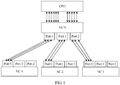
- FIG. 1 is a schematic diagram of a connection manner between a CPU and an NC according to an embodiment of this application.
- NC 0 can be connected to one CPU and a plurality of NCs.
- the NC 0 being connected to one CPU represents an example not being part of the present invention.
- the NC 0 being connected to a plurality of NCs represents an embodiment of the present invention.
- NC 0 is connected to the CPU by using 20 lanes, and is also connected to NC 1, NC 2, and NC 3 through port 0, port 1, and port 2 on NC 0 respectively.
- two ends of each lane between NC 0 and the CPU are a PHY interface of the CPU and a PHY interface of the NC.
- the PHY interface of the CPU and the PHY interface of the NC each have a sequence number, and a sequence number can indicate an order of a PHY interface in all PHY interfaces.
- a PHY interface of the CPU and a PHY interface of the NC may be connected to form a lane through cabling in a positive or reverse sequence, and the lane may be used to transmit data between the CPU and the NC.
- PHY interfaces on the CPU are connected to PHY interfaces with same sequence numbers on the NC.
- PHY 0 on the CPU is connected to PHY 0 on the NC
- PHY 1 on the CPU is connected to PHY 1 on the NC
- PHY 19 on the CPU is connected to PHY 19 on the NC. In this way, 20 lanes may be formed.
- a PHY interface with a minimum sequence number on the CPU is sequentially connected to a PHY interface with a maximum sequence number on the NC, or a PHY interface with a maximum sequence number on the CPU is sequentially connected to a PHY interface with a minimum sequence number on the NC.
- PHY 0 on the CPU is connected to PHY 19 on the NC
- PHY 1 on the CPU is connected to PHY 18 on the NC.
- 20 lanes may be formed.
- the transmit end is the CPU and the receive end is the NC, or the transmit end is the NC and the receive end is the CPU.
- the CPU sends a packet to the NC
- the CPU may be referred to as the transmit end
- the NC may be referred to as the receive end.
- the NC sends a packet to the CPU
- the NC may be referred to as the transmit end
- the CPU may be referred to as the receive end.
- data may be transmitted between the CPU and the NC in a full bandwidth transmission manner or a half bandwidth transmission manner.
- the data may be transmitted by using eight lanes between PHY 0 to PHY 7 of the transmit end and PHY 0 to PHY 7 of the receive end, or the data may be transmitted by using eight lanes between PHY 12 to PHY 19 of the transmit end and PHY 12 to PHY 19 of the receive end.
- the data When data is transmitted in the half bandwidth transmission manner in a system in which the CPU and the NC have physical cabling in a reverse sequence manner, the data may be transmitted by using eight lanes between PHY 0 to PHY 7 of the transmit end and PHY 12 to PHY 19 of the receive end, or the data may be transmitted by using eight lanes between PHY 12 to PHY 19 of the transmit end and PHY 0 to PHY 7 of the receive end.
- data When data is transmitted in the half bandwidth transmission manner, if one interface in PHY 0 to PHY 7 fails and one interface in PHY 12 to PHY 19 fails, data cannot be transmitted between the CPU and the NC.
- the transmit end when data is transmitted between NCs through a CXP interface, the transmit end may be referred to as a first NC, and the receive end may be referred to as a second NC.
- a first port of the first NC has at least two interfaces, and an interface connected to an interface on the first port is located on a second port of the second NC.
- NC 0 is connected to NC 1, NC 2, and NC 3 through port 0, port 1, the and port 2 respectively.
- the CXPs on each port has a sequence number, and the CXPs on each port are numbered independently.
- the sequence number can indicate an order of a CXP interface in all PHY interfaces on one port.
- sequence numbers of the CXPs need to be in one-to-one correspondences.
- the three CXPs on port 0 of NC 0 may be CXP 0, CXP 1, and CXP 2
- the three CXPs on port 0 of NC 1 may be CXP 0, CXP 1, and CXP 2.
- CXP 0 on port 0 of NC 0 is connected to CXP 0 on port 0 of NC 1 through an optical cable or a cable
- CXP 1 on port 0 of NC 0 is connected to CXP 1 on port 0 of NC 1 through an optical cable or a cable
- CXP 2 on port 0 of NC 0 is connected to CXP 2 on port 0 of NC 1 through an optical cable or a cable.
- NC 0 may be connected to NC 2 and NC 3 in a manner similar to the manner in which NC 0 is connected to NC 1.
- a cable or an optical cable between CXPs may also be referred to as a lane.
- the interfaces between the CPU and the NC may be connected in a disordered manner.
- the interfaces between the NCs may be connected in a disordered manner.
- the CPU and the NC may not be connected in a positive sequence or a reverse sequence, so that a PHY interface on the CPU is connected to any PHY interface on the NC to form a lane.
- the CXP interfaces between the NCs may not be connected in a manner with sequence numbers corresponding to each other one to one.
- the CXP interfaces may be inserted in a mixed manner, so that a CXP interface on a port of an NC is connected to any CXP interface on a corresponding port of another NC through an optical cable or a cable.
- physical cabling between the CPU and the NC is more flexible, and in this embodiment of the present invention, connection of the CXP interfaces between the NCs is also more flexible.
- the 20 lanes between the CPU and NC 0 in FIG. 1 may be randomly connected.
- any PHY interface on the CPU may be connected to any PHY interface on NC 0. In this way, cabling between the CPU and the NC is more flexible.
- FIG. 1 the 20 lanes between the CPU and NC 0 in FIG. 1 may be randomly connected.
- any PHY interface on the CPU may be connected to any PHY interface on NC 0. In this way, cabling between the CPU and the NC is more flexible.
- FIG. 1 in FIG.
- any CXP interface on port 0 of NC 0 may be connected to any CXP interface on port 0 of NC 1 by using an optical cable or a cable
- any CXP interface on port 1 of NC 0 may be connected to any CXP interface on port 0 of NC 2
- any CXP interface on port 2 of NC 0 may be connected to any CXP interface on port 0 of NC 3. In this way, the CXP interfaces between the NCs are connected in a more flexible manner.
- FIG. 2 is a schematic flowchart of a data transmission method according to an embodiment of this application.
- a transmit end 11 is the CPU in the foregoing description
- a receive end 12 is the NC in the foregoing description
- the transmit end 11 is the NC in the foregoing description
- the receive end 12 is the CPU in the foregoing description.
- the transmit end 11 is the first NC
- the receive end 12 is the second NC.
- the transmit end 11 obtains at least two to-be-transmitted packets.
- the transmit end may divide the to-be-transmitted data into a plurality of data packets, and encapsulate the data packets into a plurality of packets for transmission.
- the transmit end when data is transmitted between the CPU and the NC in a full bandwidth transmission manner, the transmit end may obtain 20 packets. When data is transmitted between the CPU and the NC in a half bandwidth transmission manner, the transmit end may obtain eight packets. When data is transmitted between NCs, the transmit end may obtain three packets.
- the transmit end 11 determines, in at least two interfaces of the transmit end 11, a first interface used to transmit each of the packets, and determines an identifier that is of each of the packets and that is related to the first interface.
- the identifier represents an order of the first interface used to transmit each of the packets in the at least two interfaces used to send the at least two packets.
- the order of the first interface used to transmit each of the packets in the at least two interfaces used to send the at least two packets may be a positive order or a reverse order.
- the transmit end may determine a packet to be transmitted on each lane, and determine an identifier related to the first interface for the packet.
- the transmit end when data is transmitted between the CPU and the NC in the full bandwidth transmission manner, the transmit end may determine to allocate 20 packets to 20 PHY interfaces of the transmit end, and then each PHY interface sends a packet in a sending queue of the PHY interface through a lane of the PHY interface.
- the transmit end may determine to allocate eight packets to eight PHY interfaces of the transmit end, and then each PHY interface sends a packet in a sending queue of the PHY interface through a lane.
- the transmit end may determine to allocate three packets to three CXP interfaces of the transmit end, and then each CXP interface sends a packet in a sending queue of the CXP interface through an optical cable or a cable.
- the transmit end may sort a plurality of packets. For example, after sorting, the transmit end may obtain 20 packets, which are successively packet 0, packet 1, ..., and packet 19, or obtain eight packets, which are successively packet 0, packet 1, ..., and packet 7, or obtain three packets, which are successively packet 0, packet 1, and packet 2.
- the transmit end may transmit each corresponding packet by separately using a PHY interface or a CXP interface that has a same sequence number as the packet. For example, the transmit end may sequentially transmit packet 0, packet 1, ..., and packet 19 by using PHY 0 to PHY 19, or sequentially transmit packet 0, packet 1, and packet 2 by using CXP 0 to CXP 2.
- the transmit end may sequentially allocate eight packets to eight PHY interfaces based on sequence numbers of the PHY interfaces in ascending order (or in descending order). For example, when the transmit end selects PHY 10 to PHY 17 to transmit the packets, packet 0, packet 1, ..., and packet 7 may be sequentially allocated to PHY 10 to PHY 17 for transmission. When the transmit end selects PHY 0, PHY 3, PHY 4, PHY 8, PHY 11, PHY 15, PHY 16, and PHY 17 to transmit the packets, packet 0, packet 1, ..., and packet 7 may be sequentially allocated to PHY 0, PHY 3, PHY 4, PHY 8, PHY 11, PHY 15, PHY 16, and PHY 17 for transmission.
- the transmit end After the transmit end allocates, to the packets, the interfaces used to transmit the packets, the transmit end determines, for each packet, an identifier related to an interface used to transmit the packet.
- the identifier represents an order of the first interface used to transmit each of the packets in the at least two interfaces used to send the at least two packets.
- a quantity of the at least two interfaces of the transmit end is equal to a quantity of the at least two packets, and the identifier that is of each of the packets and that is related to the first interface is an identifier of the first interface.
- the identifier that is of each of the packets and that is related to the first interface is an identifier of the first interface.
- an identifier of each packet is a sequence number of a PHY interface used for transmitting the packet. For example, when the transmit end determines to send a packet by using PHY 1, an identifier of the packet is a sequence number 1 of PHY 1. When the transmit end determines to send a packet by using PHY 4, an identifier of the packet is a sequence number 4 of PHY 4.
- a quantity of the packets is n and an order of a first interface used to transmit an i th packet in the n packets in n interfaces used to transmit the n packets is i
- an identifier that is of the i th packet and that is related to the first interface is an identifier of an i th interface at the transmit end, where a quantity of the at least two interfaces of the transmit end is greater than or equal to a quantity of the at least two packets, n is a positive integer, and i is a positive integer less than or equal to n.
- any eight lanes may be selected from the 20 lanes, for example, eight lanes corresponding to PHY 10 to PHY 17 of the transmit end may be selected, or eight lanes corresponding to PHY 0, PHY 3, PHY 4, PHY 8, PHY 11, PHY 15, PHY 16, and PHY 17 of the transmit end may be selected.
- eight packets may be allocated to interfaces corresponding to the eight lanes for transmission.
- identifiers of the packets transmitted on PHY 10 to PHY 17 are 0 to 7 in sequence, or identifiers of the packets transmitted on PHY 0, PHY 3, PHY 4, PHY 8, PHY 11, PHY 15, PHY 16, and PHY 17 are 0 to 7 in sequence.
- data may be transmitted by using the eight lanes. That is, in this example not being part of the present invention, data may be transmitted in the half bandwidth transmission manner when a plurality of PHY interfaces fail.
- the first NC when data is transmitted between the NCs through a CXP interface, the first NC may determine that an identifier that is of each packet and that is related to an interface at the transmit end is a sequence number of a CXP interface used for transmitting the packet. For example, when the transmit end determines to send a packet by using CXP 1, an identifier of the packet may be 1. When the transmit end sends a packet by using CXP 2, an identifier of the packet may be 2.
- the transmit end 11 adds the identifier to each of the packets.
- the transmit end may encapsulate the identifier of each packet into a packet header of the packet.
- the transmit end 11 sends the packet obtained in 230 to the receive end 12 through the first interface, so that the receive end 12 adjusts, based on the identifier, an order of the packet added with the identifier.
- a packet when a packet is sent between the NCs through a CXP interface, if a second interface on a first port of the first NC fails, the transmit end sends, to the receive end through a third interface on the first port, a packet added with an identifier related to the second interface. For example, when CXP 1 on port 0 of NC 0 fails, a packet allocated to CXP 1 may be transmitted through CXP 0 or CXP 2 on port 0. In this way, when a CXP interface fails, another CXP interface may be used for transmission, and the receive end can parse out the packet normally.
- the receive end receives the packet through the second interface.
- the second interface is one of the at least two interfaces of the receive end, and the second interface is disorderly connected to the first interface at the transmit end.
- the receive end 12 obtains the identifier in the packet.
- the receive end may obtain the identifier from a corresponding field in the packet header of the packet.
- the receive end 12 sends the packet to a processing queue of an interface having the identifier at the receive end 12. Specifically, after the receive end obtains an identifier that is of the packet and that is related to an interface at the transmit end, the receive end may send a second packet to the processing queue of the interface with the identifier at the receive end. In this way, in a subsequent processing queue, a packet sequence is adjusted.
- the receive end when data is transmitted between the CPU and the NC, in an example not being part of the present invention, and an identifier in a packet received by PHY 1 of the receive end is 0, the receive end sends the packet to a processing queue of a PHY interface whose identifier is 0 in the receive end, to be specific, sends the packet to a processing queue of PHY 0.
- the receive end when data is transmitted between the NCs and an identifier in a packet received by CXP 0 of the receive end is 2, the receive end sends the packet to a processing queue of a CXP interface whose identifier is 2 in the receive end, to be specific, sends the packet to a processing queue of CXP 2.
- a packet sequence is the same as a sequence in which the transmit end sends the packet. Therefore, in this embodiment of this application, when sending the at least two packets, the transmit end adds an identifier related to an interface at the transmit end to each packet, and then, in an example not being part of the present invention, sends a packet added with the identifier between a CPU and an NC that have disordered physical cabling or in an embodiment of the present invention between NCs with CXPs inserted in a mixed manner, so that the receive end can adjust a sequence of at least two received packets based on the identifier included in the packets. In this way, data can be transmitted between the CPU and the NC that have disordered physical cabling or between the NCs with CXPs inserted in the mixed manner.
- FIG. 3 is a schematic diagram of a data transmission method between a CPU and an NC in a full bandwidth manner according to an example not being part of the present invention. Reference numerals that are shown below and that are the same as those in
- FIG. 2 represent same or similar modules or units.
- a transmit end 11 may allocate packets 0 to 19 to PHY 19 to PHY 0.
- identifiers that are of the packets 0 to 19 and that are related to the interfaces of the transmit end are 19 to 0 respectively.
- packets received by PHY interfaces of a receive end 12 are disordered. For example, packets corresponding to PHY 0 to PHY 19 are successively packet 17, packet 8, packet 6, packet 1, ..., packet 0, packet 2, packet 15, and packet 19.
- the receive end 12 parses the identifier in each packet.
- the receive end may successively learn through parsing that identifiers of PHY 0 to PHY 19 are 17, 8, 6, 1, ..., 0, 2, 15 and 19. Then, the receive end 12 inputs the identifiers obtained through parsing into an adjustment unit 121, and the adjustment unit 121 transmits, based on the identifier of each packet, the packet to a processing queue with a corresponding identifier at the receive end. Specifically, the receive end transmits packet 17 with the identifier of 17 to a processing queue corresponding to PHY 17 in the receive end, and transmits packet 8 with the identifier of 8 to a processing queue corresponding to PHY 8 in the receive end. Similarly, the receive end transmits packet 6, packet 1, ..., packet 0, packet 2, packet 15 and packet 19 to processing queues corresponding to corresponding PHY interfaces in the receive end.
- FIG. 4 is a schematic diagram of a data transmission method between a CPU and an NC in a half bandwidth transmission manner according to an an example not being part of the present invention.
- a PHY interface in a transmit end 11 or a receive end 12 fails, data may be transmitted in the half bandwidth transmission manner.
- eight packets may be allocated to any eight PHY interfaces that can work normally in the transmit end 11, and an identifier of a packet to be transmitted on each PHY interface is successively determined based on orders of sequence numbers of the PHY interfaces. For example, when it is determined to transmit packets on PHY 10 to PHY 17, identifiers of packets transmitted on PHY 10 to PHY 17 are successively 0 to 7.
- the receive end 12 parses the identifiers of the eight packets, and inputs the identifiers obtained by parsing into an adjustment unit 121, and the adjustment unit 121 transmits, based on the identifier of each packet, the packet to a processing queue with a corresponding identifier at the receive end. Similarly, the receive end transmits the received packets with identifiers of 7, 3, 6, 1, 2, 5, and 4 to processing queues corresponding to PHY interfaces in the receive end.
- FIG. 5 is a schematic diagram of a data transmission method between NCs according to an embodiment of the present invention.
- a receive end shown in FIG. 5 is a first NC, and the first NC is connected to a transmit end (a second NC) through port 0.
- CXP 0, CXP 1, and CXP 2 of the second NC are connected to CXP 1, CXP 2, and CXP 0 of the first NC in a mixed manner.
- identifiers 0, 1, and 2 are added to packet headers of packet 0, packet 1, and packet 2 respectively.
- packet 1, packet 0, and packet 2 are received by CXP 0, CXP 1, and CXP 2 of the receive end (namely, the first NC) respectively, and the receive end parses out the identifier of each packet.
- the receive end inputs the identifiers obtained through parsing into an adjustment unit.
- the adjustment unit transmits, based on the identifier of each packet, the packets to processing queues with corresponding identifiers in the first NC.
- the first NC transmits the packets with identifiers 1, 0, and 2 to processing queues of CXP 1, CXP 2, and CXP 0 in the first NC respectively.
- another lane on a same port may be used to transmit a packet allocated to the lane.
- packet 0 and packet 2 that are added with identifiers may be transmitted on a lane between CXP 2 of the transmit end and CXP 0 of the receive end, and the identifier of each packet is parsed out.
- the transmit end inputs the identifiers obtained by parsing into the adjustment unit.
- the adjustment unit transmits, based on the identifier of each packet, the packets to processing queues with corresponding identifiers in the first NC.
- the first NC transmits the packets with identifiers 1, 0, and 2 to processing queues of CXP 1, CXP 2, and CXP 0 in the first NC respectively.
- the transmit end when sending the at least two packets, the transmit end adds an identifier related to an interface at the transmit end to each packet, and then, in an example not being part of the present invention, sends a packet added with the identifier between a CPU and an NC that have disordered physical cabling or, in an embodiment of the present invention, between NCs with CXPs inserted in a mixed manner, so that the receive end adjusts a sequence of at least two received packets based on the identifier included in the packets.
- data can be transmitted between the CPU and the NC that have disordered physical cabling or between the NCs with CXPs inserted in the mixed manner.
- FIG. 6 is a schematic block diagram of a device 600 for data transmission according to an embodiment of this application.
- the device 600 is a device in a processor system, and the processor system includes a first node controller NC, and further includes a CPU connected to the first NC, representing an example not being part of the present invention, or a second NC connected to the first NC, representing an embodiment of the present invention, where the device 600 is a transmit end device, the transmit end device is the first NC, the CPU, or the second NC, the transmit end device has at least two interfaces, and each interface of the transmit end device is connected to an interface of a receive end device.
- the device 600 includes an obtaining unit 610, a determining unit 620, an adding unit 630, and a sending unit 640.
- the obtaining unit 610 is configured to obtain at least two to-be-transmitted packets.
- the determining unit 620 is configured to: determine, in the at least two interfaces of the transmit end device, a first interface used to transmit each of the packets, and determine an identifier that is of each of the packets and that is related to the first interface, where the identifier represents an order of the first interface used to transmit each of the packets in the at least two interfaces used to send the at least two packets.
- the adding unit 630 is configured to add the identifier to a packet header of each of the packets.
- the sending unit 640 is configured to send, to the receive end through the first interface, a packet added with the identifier, so that the receive end device adjusts, based on the identifier, an order of the packet added with the identifier.
- the transmit end when sending the at least two packets, adds an identifier related to an interface at the transmit end to each packet, and then sends a packet added with the identifier between a CPU and an NC that have disordered physical cabling, representing an embodiment not being part of the present invention, or between NCs with CXPs inserted in a mixed manner, representing an embodiment of the present invention, so that the receive end adjusts a sequence of at least two received packets based on the identifier included in the packets.
- data can be transmitted between the CPU and the NC that have disordered physical cabling or between the NCs with CXPs inserted in the mixed manner.
- a quantity of the at least two interfaces of the transmit end device is equal to a quantity of the at least two packets, and the identifier that is of each of the packets and that is related to the first interface is an identifier used for the first interface.
- the processor system when data is transmitted between the CPU and the first NC in a half bandwidth transmission manner, if a quantity of the packets is n and an order of a first interface used to transmit an i th packet in the n packets in n interfaces used to transmit the n packets is i, an identifier that is of the i th packet and that is related to the first interface is an identifier of an i th interface at the transmit end, where a quantity of the at least two interfaces of the transmit end is greater than or equal to a quantity of the at least two packets, n is a positive integer, and i is a positive integer less than or equal to n.
- a first port of the first NC has at least two interfaces, and an interface connected to an interface on the first port is located on a second port of the second NC.
- the transmit end device sends, to the receive end device through a third interface on the first port, the packet added with an identifier related to the second interface.
- a device 700 for data transmission may include a processor 710, a memory 720, and a communications interface 730.
- the processor 710 may be configured to determine information to be sent by the communications interface 730, and the memory 720 may be configured to store code executed by the processor 710.
- the processor 710, the memory 720, and the communications interface 730 communicate with one another through an internal connection channel, to transmit a control signal and/or a data signal.
- the memory may be a separate device, or may be integrated into the processor. All or some of the foregoing components may be integrated into a chip for implementation, for example, integrated into a baseband chip for implementation.
- the memory 720 is configured to store program code.
- the processor 710 is configured to execute the program code stored in the memory 720, and when the program code is executed, the processor 710 is configured to obtain at least two to-be-transmitted packets.
- the processor 710 is further configured to: determine, in the at least two interfaces of the transmit end device, a first interface used to transmit each of the packets, and determine an identifier that is of each of the packets and that is related to the first interface, where the identifier represents an order of the first interface used to transmit each of the packets in the at least two interfaces used to send the at least two packets.
- the processor 710 is further configured to add the identifier to a packet header of each of the packets.
- the communications interface 730 is configured to send, to the receive end through the first interface, a packet added with the identifier, so that the receive end device adjusts, based on the identifier, an order of the packet added with the identifier.
- units in the device 700 for data transmission are separately configured to perform actions or processing processes performed by the transmit end device in the foregoing methods. To avoid repetition, detailed descriptions thereof are omitted herein.
- the foregoing device 700 for data transmission may be a CPU or an NC in a processor system.
- the processor may be an integrated circuit chip and has a signal processing capability.
- the steps in the foregoing method embodiments may be implemented by using a hardware integrated logical circuit in the processor, or by using instructions in a form of software.
- the foregoing processor may be a central processing unit (central processing unit, CPU), and the processor may further be another general purpose processor, a digital signal processor (digital signal processor, DSP), an application-specific integrated circuit (application-specific integrated circuit, ASIC), a field programmable gate array (field programmable gate array, FPGA) or another programmable logical device, a discrete gate or transistor logic device, or a discrete hardware component.
- DSP digital signal processor
- ASIC application-specific integrated circuit
- FPGA field programmable gate array
- the processor may implement or perform the methods, the steps, and logical block diagrams that are disclosed in the embodiments of this application.
- the general purpose processor may be a microprocessor, any conventional processor, or the like.
- the steps of the method disclosed with reference to the embodiments of this application may be directly performed by using a hardware decoding processor, or may be performed by using a combination of hardware and a software unit in the decoding processor.
- the software unit may be located in a mature storage medium in the art, such as a random access memory, a flash memory, a read-only memory, a programmable read-only memory, an electrically erasable programmable memory, or a register.
- the storage medium is located in the memory, and the processor reads information in the memory and completes the steps in the foregoing method in combination with hardware of the processor.
- the memory in this embodiment of this application may be a volatile memory or a nonvolatile memory, or may include a volatile memory and a nonvolatile memory.
- the nonvolatile memory may be a read-only memory (read-only memory, ROM), a programmable read-only memory (programmable ROM, PROM), an erasable programmable read-only memory (erasable PROM, EPROM), an electrically erasable programmable read-only memory (electrically EPROM, EEPROM), or a flash memory.
- the volatile memory may be a random access memory (random access memory, RAM), used as an external cache.
- RAMs may be used, for example, a static random access memory (static RAM, SRAM), a dynamic random access memory (dynamic RAM, DRAM), a synchronous dynamic random access memory (synchronous DRAM, SDRAM), a double data rate synchronous dynamic random access memory (double data rate SDRAM, DDR SDRAM), an enhanced synchronous dynamic random access memory (enhanced SDRAM, ESDRAM), a synchlink dynamic random access memory (synchlink DRAM, SLDRAM), and a direct rambus random access memory (direct rambus RAM, DRRAM).
- static random access memory static random access memory
- DRAM dynamic random access memory
- DRAM dynamic random access memory
- SDRAM synchronous dynamic random access memory
- double data rate SDRAM double data rate SDRAM
- DDR SDRAM double data rate SDRAM
- ESDRAM enhanced synchronous dynamic random access memory
- synchlink dynamic random access memory synchlink dynamic random access memory
- direct rambus RAM direct rambus RAM
- a network device or a terminal device in an apparatus embodiment fully corresponds to a network device or a terminal device in a method embodiment.
- a corresponding module performs a corresponding step.
- a sending module or a transmitter performs a sending step in the method embodiment
- a receiving module or a receiver performs a receiving step in the method embodiment. Steps other than the sending and receiving steps may be performed by a processing module or a processor.
- a processing module or a processor For a function of a specific module, refer to a corresponding method embodiment. Details are not described herein again.
- the steps in the foregoing method may be implemented by using a hardware integrated logical circuit in the processor 710, or by using instructions in a form of software.
- the steps of the method disclosed with reference to the embodiments of this application may be directly performed by using a hardware processor, or may be performed by using a combination of hardware and a software module in the processor.
- the software module may be located in a mature storage medium in the art, such as a random access memory, a flash memory, a read-only memory, a programmable read-only memory, an electrically erasable programmable memory, or a register.
- the storage medium is located in the memory 720, and the processor 710 reads information in the memory 720 and completes the steps in the foregoing methods in combination with hardware of the processor. To avoid repetition, details are not described herein again.
- FIG. 8 is a schematic block diagram of a device 800 for data transmission according to an embodiment of this application.
- the device 800 is a device in a processor system, and the processor system includes a first node controller NC, and further includes a CPU connected to the first NC, representing an example not being part of the present invention, or a second NC connected to the first NC, representing an embodiment of the present invention, where the device is a receive end device, the receive end device is the first NC, the CPU, or the second NC, the receive end device has at least two interfaces, and each interface of the received end device is connected to an interface at a transmit end device.
- the device 800 includes a receiving unit 810, an obtaining unit 820 and a sending unit 830.
- the receiving unit 810 is configured to receive, through a second interface in the at least two interfaces, a packet sent by the transmit end through a first interface, where the second interface is connected to the first interface, the packet includes an identifier related to the first interface, and the identifier represents an order of the first interface in at least two interfaces that are at the transmit end and that are used to send at least two packets.
- the obtaining unit 820 is configured to obtain the identifier in the packet.
- the sending unit 830 is configured to send the packet to a processing queue of an interface having the identifier at the receive end.
- the transmit end when sending the at least two packets, adds an identifier related to an interface at the transmit end to each packet, and then sends a packet added with the identifier between a CPU and an NC that have disordered physical cabling, representing an example not being part of the present invention, or between NCs with CXPs inserted in a mixed manner, representing an embodiment of the present invention, so that the receive end can adjust a sequence of at least two received packets based on the identifier included in the packets. In this way, data can be transmitted between the CPU and the NC that have disordered physical cabling or between the NCs with CXPs inserted in the mixed manner.
- a quantity of the at least two interfaces of the receive end device is equal to a quantity of the packets, and the identifier that is in each of the packet and that is related to the first interface is an identifier of the first interface.
- a first port of the first NC has at least two interfaces, and an interface that is in the second NC and that is connected to an interface on the first port is located on a second port of the second NC.
- a device 900 for data transmission may include a processor 910, a memory 920, and a communications interface 930.
- the processor 910 may be configured to determine information received by the communications interface 930, and the memory 920 may be configured to store code executed by the processor 910.
- the processor 910, the memory 920, and the communications interface 930 communicate with one another through an internal connection channel, to transmit a control signal and/or a data signal.
- the memory may be a separate device, or may be integrated into the processor. All or some of the foregoing components may be integrated into a chip for implementation, for example, integrated into a baseband chip for implementation.
- the memory 920 is configured to store program code.
- the communications interface 930 is configured to receive, through a second interface in the at least two interfaces, a packet sent by the transmit end through a first interface, where the second interface is connected to the first interface, the packet includes an identifier related to the first interface, and the identifier represents an order of the first interface in at least two interfaces that are at the transmit end and that are used to send at least two packets.
- the processor 910 is configured to execute the program code stored in the memory 920, and when the program code is executed, the processor 910 is configured to obtain the identifier of the packet.
- the processor 910 is further configured to send the packet to a processing queue of an interface having the identifier at the receive end.
- units in the device 900 for data transmission are separately configured to perform actions or processing processes performed by the receive end device in the foregoing methods. To avoid repetition, detailed descriptions thereof are omitted herein.
- the foregoing device 900 for data transmission may be a CPU or an NC in a processor system.
- the processor may be an integrated circuit chip and has a signal processing capability.
- the steps in the foregoing method embodiments may be implemented by using a hardware integrated logical circuit in the processor, or by using instructions in a form of software.
- the foregoing processor may be a central processing unit (central processing unit, CPU), and the processor may further be another general purpose processor, a digital signal processor (digital signal processor, DSP), an application-specific integrated circuit (application-specific integrated circuit, ASIC), a field programmable gate array (field programmable gate array, FPGA) or another programmable logical device, a discrete gate or transistor logic device, or a discrete hardware component.
- DSP digital signal processor
- ASIC application-specific integrated circuit
- FPGA field programmable gate array
- the processor may implement or perform the methods, the steps, and logical block diagrams that are disclosed in the embodiments of this application.
- the general purpose processor may be a microprocessor, any conventional processor, or the like.
- the steps of the method disclosed with reference to the embodiments of this application may be directly performed by using a hardware decoding processor, or may be performed by using a combination of hardware and a software unit in the decoding processor.
- the software unit may be located in a mature storage medium in the art, such as a random access memory, a flash memory, a read-only memory, a programmable read-only memory, an electrically erasable programmable memory, or a register.
- the storage medium is located in the memory, and the processor reads information in the memory and completes the steps in the foregoing method in combination with hardware of the processor.
- the memory in this embodiment of this application may be a volatile memory or a nonvolatile memory, or may include a volatile memory and a nonvolatile memory.
- the nonvolatile memory may be a read-only memory (read-only memory, ROM), a programmable read-only memory (programmable ROM, PROM), an erasable programmable read-only memory (erasable PROM, EPROM), an electrically erasable programmable read-only memory (electrically EPROM, EEPROM), or a flash memory.
- the volatile memory may be a random access memory (random access memory, RAM), used as an external cache.
- RAMs may be used, for example, a static random access memory (static RAM, SRAM), a dynamic random access memory (dynamic RAM, DRAM), a synchronous dynamic random access memory (synchronous DRAM, SDRAM), a double data rate synchronous dynamic random access memory (double data rate SDRAM, DDR SDRAM), an enhanced synchronous dynamic random access memory (enhanced SDRAM, ESDRAM), a synchlink dynamic random access memory (synchlink DRAM, SLDRAM), and a direct rambus random access memory (direct rambus RAM, DRRAM).
- static random access memory static random access memory
- DRAM dynamic random access memory
- DRAM dynamic random access memory
- SDRAM synchronous dynamic random access memory
- double data rate SDRAM double data rate SDRAM
- DDR SDRAM double data rate SDRAM
- ESDRAM enhanced synchronous dynamic random access memory
- synchlink dynamic random access memory synchlink dynamic random access memory
- direct rambus RAM direct rambus RAM
- a network device or a terminal device in an apparatus embodiment fully corresponds to a network device or a terminal device in a method embodiment.
- a corresponding module performs a corresponding step.
- a sending module or a transmitter performs a sending step in the method embodiment
- a receiving module or a receiver performs a receiving step in the method embodiment. Steps other than the sending and receiving steps may be performed by a processing module or a processor.
- a processing module or a processor For a function of a specific module, refer to a corresponding method embodiment. Details are not described herein again.
- the steps in the foregoing method may be implemented by using a hardware integrated logical circuit in the processor 910, or by using instructions in a form of software.
- the steps of the method disclosed with reference to the embodiments of this application may be directly performed by using a hardware processor, or may be performed by using a combination of hardware and a software module in the processor.
- the software module may be located in a mature storage medium in the art, such as a random access memory, a flash memory, a read-only memory, a programmable read-only memory, an electrically erasable programmable memory, or a register.
- the storage medium is located in the memory 920, and the processor 910 reads information in the memory 920 and completes the steps in the foregoing methods in combination with hardware of the processor. To avoid repetition, details are not described herein again.
- sequence numbers of the foregoing processes do not mean performing sequences in various embodiments of this application.
- the performing sequences of the processes should be determined based on functions and internal logic of the processes, and should not be construed as any limitation on the implementation processes of the embodiments of this application.
- the disclosed system, apparatus, and method may be implemented in other manners.
- the described apparatus embodiment is merely an example.
- the unit division is merely logical function division and may be other division in actual implementation.
- a plurality of units or components may be combined or integrated into another system, or some features may be ignored or not performed.
- the displayed or discussed mutual couplings, direct couplings or communication connections may be implemented by using some interfaces. Indirect couplings or communication connections between the apparatuses or units may be implemented in electronic, mechanical, or other forms.
- the units described as separate parts may or may not be physically separate, and parts displayed as units may or may not be physical units, may be located in one position, or may be distributed on a plurality of network units. Some or all of the units may be selected based on actual requirements to achieve the objectives of the solutions of the embodiments.
- All or some of the foregoing embodiments may be implemented by using software, hardware, firmware, or any combination thereof.
- the embodiments may be implemented completely or partially in a form of a computer program product.
- the computer program product includes one or more computer instructions.
- the computer may be a general-purpose computer, a dedicated computer, a computer network, or another programmable apparatus.
- the computer instructions may be stored in a computer-readable storage medium or may be transmitted from a computer-readable storage medium to another computer-readable storage medium.
- the computer instructions may be transmitted from a website, computer, server, or data center to another website, computer, server, or data center in a wired (for example, a coaxial cable, an optical fiber, or a digital subscriber line (DSL)) or wireless (for example, infrared, radio, or microwave) manner.
- the computer-readable storage medium may be any usable medium accessible by a computer, or a data storage device, such as a server or a data center, integrating one or more usable media.
- the usable medium may be a magnetic medium (for example, a floppy disk, a hard disk, or a magnetic tape), an optical medium (for example, a DVD), or a semiconductor medium (for example, a solid state disk (Solid State Disk, SSD)).
- a magnetic medium for example, a floppy disk, a hard disk, or a magnetic tape
- an optical medium for example, a DVD
- a semiconductor medium for example, a solid state disk (Solid State Disk, SSD)
Landscapes
- Engineering & Computer Science (AREA)
- Computer Networks & Wireless Communication (AREA)
- Signal Processing (AREA)
- Computer Security & Cryptography (AREA)
- Theoretical Computer Science (AREA)
- General Physics & Mathematics (AREA)
- General Engineering & Computer Science (AREA)
- Physics & Mathematics (AREA)
- Computer Hardware Design (AREA)
- Software Systems (AREA)
- Communication Control (AREA)
- Data Exchanges In Wide-Area Networks (AREA)
- Computer And Data Communications (AREA)
Description
- This application relates to the communications field, and more specifically, to a data transmission method and device in the communications field.
- With progress of technologies, a higher requirement is raised on processor performance. To meet this requirement, a processor system with a stronger processing capability is developed, for example, a symmetric multi-processor (Symmetric Multi-Processor, SMP) system, a cluster (Cluster) system, a massively parallel processing (Massively Parallel Processing, MPP) system, a non-uniform memory access (Non-Uniform Memory Access, NUMA) system, or another processor system architecture. These architectures improve system performance mainly through memory and bus sharing. For example, in the NUMA system architecture, nodes connect to each other and exchange information in an interconnection mode. In one operating system, all CPUs and memories of the entire system may be shared, thereby improving and optimizing performance of the processor system.
- A node controller (Node Controller, NC) is a chip used for central processing unit (Central Processing Unit, CPU) extension, and can implement interconnection between a plurality of CPUs. The node controller is connected to the CPUs by using 20 lanes (lane), and is also connected to another NC through a port. However, at present, a physical (PHY) interface between an NC and a CPU supports only positive sequence connection and reverse sequence connection, and one-to-one connection of optical ports (CXP) on a port needs to be supported between NCs. As a result, connection between an NC and a CPU and connection between NCs have low flexibility.
-
US 2016/0283429 A1 discloses a system-on-chip divided into hard IP blocks with fixed routing and soft IP blocks with flexible routing. Bowtie routing is avoided by the use of a multiplexer-like programmable switch within the soft IP. - Conference paper "HHMA: A Hierarchical Hybrid Memory Architecture Sharing Multi-Port Memory" by Caixia Liu, et al. at "Young Computer Scientists, 2008", IEEE, Piscataway, NJ, USA, November 2008, discloses a hierarchical hybrid memory architecture sharing multi-port memory.
-
US 2009/213868 A1 discloses a port interface that is arranged and configured to receive a packet from an ingress port, a traffic management module being operatively coupled to the port interface and that is arranged and configured to manage routing of the packet to a destination, and a packet processing engine that is arranged and configured to perform packet processing on the packet and to associate a tag with the packet, where the tag includes a packet processing source field, a destination field, and a fabric source field. -
US2013073814 discloses a multi-node interconnection architecture interconnecting node controllers in a one-to-one relationship. - This application provides a data transmission method, so that data can be transmitted between NCs with CXPs inserted in a mixed manner. The present invention is defined according to the independent claims.
- In the following, parts of the description and drawing referring to embodiments, which are not covered by the claims, are not presented as embodiments of the invention, but as examples useful for understanding the invention.
- In a first aspect, an embodiment of this application comprises that when sending the at least two packets, the transmit end adds an identifier related to an interface at the transmit end to each packet, and then sends a packet added with the identifier between NCs with CXPs inserted in a mixed manner, so that the receive end adjusts a sequence of at least two received packets based on the identifier included in the packets. In this way, data can be transmitted between the NCs with CXPs inserted in the mixed manner. Interfaces between the NCs are connected in a disordered manner. In addition, CXP interfaces between the NCs are not connected in a manner with sequence numbers corresponding to each other one to one. To be specific, the CXP interfaces are inserted in a mixed manner, so that a CXP interface on a port of an NC is connected to any CXP interface on a corresponding port of another NC through an optical cable or a cable. In this embodiment of this application, connection of the CXP interfaces between the NCs is also more flexible. As an example, an identifier of each packet is a sequence number of a PHY interface used for transmitting the packet, and a quantity of CXP interfaces on each port of the NC may be 3. Three optical cables or cables may be inserted in the mixed manner between NCs to transmit data.
- When the transmit end determines to transmit packets by using all the interfaces, the transmit end may transmit each corresponding packet by separately using a PHY interface or a CXP interface that has a same sequence number as the packet. For example, the transmit end may sequentially transmit
packet 0,packet 1, ..., andpacket 19 by usingPHY 0 toPHY 19, or sequentially transmitpacket 0,packet 1, andpacket 2 by usingCXP 0 toCXP 2. - According to a second aspect, a node controller NC for data transmission is provided. The NC may be implemented by hardware, or may be implemented by hardware by executing corresponding software. The hardware or software includes one or more modules corresponding to the foregoing function corresponding to the foregoing method.
- According to a third aspect, a node controller NC for data reception is provided.
- The NC includes a memory, a processor, and a communications interface, where the memory is configured to store program code, and the processor is configured to support the NC in executing a corresponding function in the foregoing method and is also configured to execute the program code stored in the memory. The communications interface is configured to support communication between the NC and another NC.
-
-
FIG. 1 is a schematic diagram of a connection manner between a CPU and an NC according to a non-claimed embodiment of this application; -
FIG. 2 is a schematic flowchart of a data transmission method according to a non-claimed embodiment of this application; -
FIG. 3 is a schematic diagram of a data transmission method between a CPU and an NC in a full bandwidth transmission manner according to a non-claimed embodiment of this application; -
FIG. 4 is a schematic diagram of a data transmission method between a CPU and an NC in a half bandwidth transmission manner according to a non-claimed embodiment of this application; -
FIG. 5 is a schematic diagram of a data transmission method between NCs according to the claimed embodiment of this application; -
FIG. 6 is a schematic block diagram of a data transmission device according to a claimed embodiment of this application; -
FIG. 7 is a schematic block diagram of a data transmission device according to a non-claimed embodiment of this application; -
FIG. 8 is a schematic block diagram of a data transmission device according to a claimed embodiment of this application; and -
FIG. 9 is a schematic block diagram of a data transmission device according to a non-claimed embodiment of this application. - The following describes the technical solutions of this application with reference to the accompanying drawings.
-
FIG. 1 is a schematic diagram of a connection manner between a CPU and an NC according to an embodiment of this application. InFIG. 1 ,NC 0 can be connected to one CPU and a plurality of NCs. TheNC 0 being connected to one CPU represents an example not being part of the present invention. TheNC 0 being connected to a plurality of NCs represents an embodiment of the present invention. Specifically,NC 0 is connected to the CPU by using 20 lanes, and is also connected toNC 1,NC 2, andNC 3 throughport 0,port 1, andport 2 onNC 0 respectively. - Specifically, two ends of each lane between
NC 0 and the CPU are a PHY interface of the CPU and a PHY interface of the NC. Herein, the PHY interface of the CPU and the PHY interface of the NC each have a sequence number, and a sequence number can indicate an order of a PHY interface in all PHY interfaces. In the prior art, a PHY interface of the CPU and a PHY interface of the NC may be connected to form a lane through cabling in a positive or reverse sequence, and the lane may be used to transmit data between the CPU and the NC. - During cabling in a positive sequence, PHY interfaces on the CPU are connected to PHY interfaces with same sequence numbers on the NC. For example,
PHY 0 on the CPU is connected toPHY 0 on the NC,PHY 1 on the CPU is connected toPHY 1 on the NC, andPHY 19 on the CPU is connected toPHY 19 on the NC. In this way, 20 lanes may be formed. - During cabling in a reverse sequence, a PHY interface with a minimum sequence number on the CPU is sequentially connected to a PHY interface with a maximum sequence number on the NC, or a PHY interface with a maximum sequence number on the CPU is sequentially connected to a PHY interface with a minimum sequence number on the NC. For example,
PHY 0 on the CPU is connected toPHY 19 on the NC, andPHY 1 on the CPU is connected toPHY 18 on the NC. Based on a similar cabling manner, 20 lanes may be formed. - In an example not being part of the present invention the transmit end is the CPU and the receive end is the NC, or the transmit end is the NC and the receive end is the CPU. Specifically, when the CPU sends a packet to the NC, the CPU may be referred to as the transmit end, and the NC may be referred to as the receive end. When the NC sends a packet to the CPU, the NC may be referred to as the transmit end, and the CPU may be referred to as the receive end.
- Herein, data may be transmitted between the CPU and the NC in a full bandwidth transmission manner or a half bandwidth transmission manner. When data is transmitted in the half bandwidth transmission manner in a system in which the CPU and the NC have positive-sequence physical cabling, the data may be transmitted by using eight lanes between
PHY 0 toPHY 7 of the transmit end andPHY 0 toPHY 7 of the receive end, or the data may be transmitted by using eight lanes betweenPHY 12 to PHY 19 of the transmit end andPHY 12 to PHY 19 of the receive end. When data is transmitted in the half bandwidth transmission manner in a system in which the CPU and the NC have physical cabling in a reverse sequence manner, the data may be transmitted by using eight lanes betweenPHY 0 toPHY 7 of the transmit end andPHY 12 to PHY 19 of the receive end, or the data may be transmitted by using eight lanes betweenPHY 12 to PHY 19 of the transmit end andPHY 0 toPHY 7 of the receive end. When data is transmitted in the half bandwidth transmission manner, if one interface inPHY 0 toPHY 7 fails and one interface inPHY 12 toPHY 19 fails, data cannot be transmitted between the CPU and the NC. - In this embodiment of this application, when data is transmitted between NCs through a CXP interface, the transmit end may be referred to as a first NC, and the receive end may be referred to as a second NC. A first port of the first NC has at least two interfaces, and an interface connected to an interface on the first port is located on a second port of the second NC.
- For example, in
FIG. 1 ,NC 0 is connected toNC 1,NC 2, andNC 3 throughport 0,port 1, the andport 2 respectively. There are three CXPs on each port on an NC. The CXPs on each port has a sequence number, and the CXPs on each port are numbered independently. The sequence number can indicate an order of a CXP interface in all PHY interfaces on one port. - In the prior art, when the three CXPs on one port of the first NC are connected to the three CXPs on a corresponding port of the second NC, sequence numbers of the CXPs need to be in one-to-one correspondences. For example, the three CXPs on
port 0 ofNC 0 may beCXP 0,CXP 1, andCXP 2, and the three CXPs onport 0 ofNC 1 may beCXP 0,CXP 1, andCXP 2. In addition,CXP 0 onport 0 ofNC 0 is connected toCXP 0 onport 0 ofNC 1 through an optical cable or a cable,CXP 1 onport 0 ofNC 0 is connected toCXP 1 onport 0 ofNC 1 through an optical cable or a cable, andCXP 2 onport 0 ofNC 0 is connected toCXP 2 onport 0 ofNC 1 through an optical cable or a cable. It may be understood thatNC 0 may be connected toNC 2 andNC 3 in a manner similar to the manner in whichNC 0 is connected toNC 1. Herein, a cable or an optical cable between CXPs may also be referred to as a lane. - It can be learned that, in the prior art, PHY interfaces between a CPU and an NC need to be connected through cabling in a positive or reverse sequence, and CXP interfaces between NCs also need to be connected in one-to-one correspondences. In other words, in the prior art, the interfaces between the CPU and the NC or between the NCs need to be connected in a fixed connection manner, and flexibility is low. In addition, the CXP interfaces between the NCs need to be connected manually, and when the CXP interfaces are connected incorrectly, a packet cannot be identified, and it is difficult to locate a fault.
- In this example not being part of the present invention, the interfaces between the CPU and the NC may be connected in a disordered manner. In this embodiment of the present invention, the interfaces between the NCs may be connected in a disordered manner. To be specific, in this example not being part of the present invention the CPU and the NC may not be connected in a positive sequence or a reverse sequence, so that a PHY interface on the CPU is connected to any PHY interface on the NC to form a lane. In addition, in this embodiment of the present invention, the CXP interfaces between the NCs may not be connected in a manner with sequence numbers corresponding to each other one to one. To be specific, the CXP interfaces may be inserted in a mixed manner, so that a CXP interface on a port of an NC is connected to any CXP interface on a corresponding port of another NC through an optical cable or a cable. In this example not being part of the present invention , physical cabling between the CPU and the NC is more flexible, and in this embodiment of the present invention, connection of the CXP interfaces between the NCs is also more flexible. For example, the 20 lanes between the CPU and
NC 0 inFIG. 1 may be randomly connected. Specifically, any PHY interface on the CPU may be connected to any PHY interface onNC 0. In this way, cabling between the CPU and the NC is more flexible. In addition, inFIG. 1 , any CXP interface onport 0 ofNC 0 may be connected to any CXP interface onport 0 ofNC 1 by using an optical cable or a cable, any CXP interface onport 1 ofNC 0 may be connected to any CXP interface onport 0 ofNC 2, and any CXP interface onport 2 ofNC 0 may be connected to any CXP interface onport 0 ofNC 3. In this way, the CXP interfaces between the NCs are connected in a more flexible manner. -
FIG. 2 is a schematic flowchart of a data transmission method according to an embodiment of this application. In the method, in a part of the method representing an example not being part of the present invention, a transmitend 11 is the CPU in the foregoing description, a receiveend 12 is the NC in the foregoing description, or the transmitend 11 is the NC in the foregoing description, and the receiveend 12 is the CPU in the foregoing description. Alternatively, in the method in a part representing an embodiment of the present invention the transmitend 11 is the first NC, and the receiveend 12 is the second NC. - 210. The transmit
end 11 obtains at least two to-be-transmitted packets. - When the transmit end needs to send data to the receive end, the transmit end may divide the to-be-transmitted data into a plurality of data packets, and encapsulate the data packets into a plurality of packets for transmission.
- Specifically, when data is transmitted between the CPU and the NC in a full bandwidth transmission manner, the transmit end may obtain 20 packets. When data is transmitted between the CPU and the NC in a half bandwidth transmission manner, the transmit end may obtain eight packets. When data is transmitted between NCs, the transmit end may obtain three packets.
- 220. The transmit
end 11 determines, in at least two interfaces of the transmitend 11, a first interface used to transmit each of the packets, and determines an identifier that is of each of the packets and that is related to the first interface. The identifier represents an order of the first interface used to transmit each of the packets in the at least two interfaces used to send the at least two packets. Herein, the order of the first interface used to transmit each of the packets in the at least two interfaces used to send the at least two packets may be a positive order or a reverse order. - In other words, the transmit end may determine a packet to be transmitted on each lane, and determine an identifier related to the first interface for the packet.
- Specifically, in this example not being part of the present invention, when data is transmitted between the CPU and the NC in the full bandwidth transmission manner, the transmit end may determine to allocate 20 packets to 20 PHY interfaces of the transmit end, and then each PHY interface sends a packet in a sending queue of the PHY interface through a lane of the PHY interface. When data is transmitted between the CPU and the NC in the half bandwidth transmission manner, the transmit end may determine to allocate eight packets to eight PHY interfaces of the transmit end, and then each PHY interface sends a packet in a sending queue of the PHY interface through a lane. When data is transmitted between the NCs, representing an embodiment of the present invention, the transmit end may determine to allocate three packets to three CXP interfaces of the transmit end, and then each CXP interface sends a packet in a sending queue of the CXP interface through an optical cable or a cable.
- As an example, the transmit end may sort a plurality of packets. For example, after sorting, the transmit end may obtain 20 packets, which are successively
packet 0,packet 1, ..., andpacket 19, or obtain eight packets, which are successivelypacket 0,packet 1, ..., andpacket 7, or obtain three packets, which are successivelypacket 0,packet 1, andpacket 2. - When the transmit end determines to transmit packets by using all the interfaces, the transmit end may transmit each corresponding packet by separately using a PHY interface or a CXP interface that has a same sequence number as the packet. For example, the transmit end may sequentially transmit
packet 0,packet 1, ..., andpacket 19 by usingPHY 0 toPHY 19, or sequentially transmitpacket 0,packet 1, andpacket 2 by usingCXP 0 toCXP 2. - When data is transmitted between the CPU and the NC in the half bandwidth transmission manner, the transmit end may sequentially allocate eight packets to eight PHY interfaces based on sequence numbers of the PHY interfaces in ascending order (or in descending order). For example, when the transmit end selects PHY 10 to PHY 17 to transmit the packets,
packet 0,packet 1, ..., andpacket 7 may be sequentially allocated to PHY 10 to PHY 17 for transmission. When the transmit end selectsPHY 0,PHY 3,PHY 4,PHY 8,PHY 11, PHY 15,PHY 16, andPHY 17 to transmit the packets,packet 0,packet 1, ..., andpacket 7 may be sequentially allocated toPHY 0,PHY 3,PHY 4,PHY 8,PHY 11, PHY 15,PHY 16, andPHY 17 for transmission. After the transmit end allocates, to the packets, the interfaces used to transmit the packets, the transmit end determines, for each packet, an identifier related to an interface used to transmit the packet. The identifier represents an order of the first interface used to transmit each of the packets in the at least two interfaces used to send the at least two packets. - Optionally, in this example not being part of the present invention, when data is transmitted between the CPU and the NC in the full bandwidth transmission manner, a quantity of the at least two interfaces of the transmit end is equal to a quantity of the at least two packets, and the identifier that is of each of the packets and that is related to the first interface is an identifier of the first interface. Alternatively, when data is transmitted between the CPU and the NC in the half bandwidth transmission manner, the identifier that is of each of the packets and that is related to the first interface is an identifier of the first interface.
- As an example, an identifier of each packet is a sequence number of a PHY interface used for transmitting the packet. For example, when the transmit end determines to send a packet by using
PHY 1, an identifier of the packet is asequence number 1 ofPHY 1. When the transmit end determines to send a packet by usingPHY 4, an identifier of the packet is asequence number 4 ofPHY 4. - Optionally, in this example not being part of the present invention, when data is transmitted between the CPU and the NC in the half bandwidth transmission manner, if a quantity of the packets is n and an order of a first interface used to transmit an ith packet in the n packets in n interfaces used to transmit the n packets is i, an identifier that is of the ith packet and that is related to the first interface is an identifier of an ith interface at the transmit end, where a quantity of the at least two interfaces of the transmit end is greater than or equal to a quantity of the at least two packets, n is a positive integer, and i is a positive integer less than or equal to n.
- As an example, when data is transmitted in the half bandwidth transmission manner, any eight lanes may be selected from the 20 lanes, for example, eight lanes corresponding to PHY 10 to PHY 17 of the transmit end may be selected, or eight lanes corresponding to
PHY 0,PHY 3,PHY 4,PHY 8,PHY 11, PHY 15,PHY 16, andPHY 17 of the transmit end may be selected. In this case, eight packets may be allocated to interfaces corresponding to the eight lanes for transmission. In this case, it may be determined that identifiers of the packets transmitted on PHY 10 toPHY 17 are 0 to 7 in sequence, or identifiers of the packets transmitted onPHY 0,PHY 3,PHY 4,PHY 8,PHY 11, PHY 15,PHY 16, andPHY 17 are 0 to 7 in sequence. In this way, provided that there are at least eight available lanes between the CPU and the NC, data may be transmitted by using the eight lanes. That is, in this example not being part of the present invention, data may be transmitted in the half bandwidth transmission manner when a plurality of PHY interfaces fail. - Optionally, in this embodiment being part of the present invention, when data is transmitted between the NCs through a CXP interface, the first NC may determine that an identifier that is of each packet and that is related to an interface at the transmit end is a sequence number of a CXP interface used for transmitting the packet. For example, when the transmit end determines to send a packet by using
CXP 1, an identifier of the packet may be 1. When the transmit end sends a packet by usingCXP 2, an identifier of the packet may be 2. - 230. The transmit
end 11 adds the identifier to each of the packets. - Specifically, the transmit end may encapsulate the identifier of each packet into a packet header of the packet.
- 240. The transmit
end 11 sends the packet obtained in 230 to the receiveend 12 through the first interface, so that the receiveend 12 adjusts, based on the identifier, an order of the packet added with the identifier. - Optionally, when a packet is sent between the NCs through a CXP interface, if a second interface on a first port of the first NC fails, the transmit end sends, to the receive end through a third interface on the first port, a packet added with an identifier related to the second interface. For example, when
CXP 1 onport 0 ofNC 0 fails, a packet allocated toCXP 1 may be transmitted throughCXP 0 orCXP 2 onport 0. In this way, when a CXP interface fails, another CXP interface may be used for transmission, and the receive end can parse out the packet normally. - After the transmit end sends the packet to the receive end, the receive end receives the packet through the second interface. The second interface is one of the at least two interfaces of the receive end, and the second interface is disorderly connected to the first interface at the transmit end.
- 250. The receive
end 12 obtains the identifier in the packet. - Specifically, the receive end may obtain the identifier from a corresponding field in the packet header of the packet.
- 260. The receive
end 12 sends the packet to a processing queue of an interface having the identifier at the receiveend 12. Specifically, after the receive end obtains an identifier that is of the packet and that is related to an interface at the transmit end, the receive end may send a second packet to the processing queue of the interface with the identifier at the receive end. In this way, in a subsequent processing queue, a packet sequence is adjusted. - For example, when data is transmitted between the CPU and the NC, in an example not being part of the present invention, and an identifier in a packet received by
PHY 1 of the receive end is 0, the receive end sends the packet to a processing queue of a PHY interface whose identifier is 0 in the receive end, to be specific, sends the packet to a processing queue ofPHY 0. In an embodiment of the present invention, when data is transmitted between the NCs and an identifier in a packet received byCXP 0 of the receive end is 2, the receive end sends the packet to a processing queue of a CXP interface whose identifier is 2 in the receive end, to be specific, sends the packet to a processing queue ofCXP 2. In this way, in a subsequent processing queue, a packet sequence is the same as a sequence in which the transmit end sends the packet. Therefore, in this embodiment of this application, when sending the at least two packets, the transmit end adds an identifier related to an interface at the transmit end to each packet, and then, in an example not being part of the present invention, sends a packet added with the identifier between a CPU and an NC that have disordered physical cabling or in an embodiment of the present invention between NCs with CXPs inserted in a mixed manner, so that the receive end can adjust a sequence of at least two received packets based on the identifier included in the packets. In this way, data can be transmitted between the CPU and the NC that have disordered physical cabling or between the NCs with CXPs inserted in the mixed manner. -
FIG. 3 is a schematic diagram of a data transmission method between a CPU and an NC in a full bandwidth manner according to an example not being part of the present invention. Reference numerals that are shown below and that are the same as those in -
FIG. 2 represent same or similar modules or units. Herein, a transmitend 11 may allocatepackets 0 to 19 toPHY 19 toPHY 0. In this case, identifiers that are of thepackets 0 to 19 and that are related to the interfaces of the transmit end are 19 to 0 respectively. Because physical cabling between the CPU and the NC is disordered, packets received by PHY interfaces of a receiveend 12 are disordered. For example, packets corresponding toPHY 0 to PHY 19 are successivelypacket 17,packet 8,packet 6,packet 1, ...,packet 0,packet 2, packet 15, andpacket 19. After receiving the packets, the receiveend 12 parses the identifier in each packet. For example, the receive end may successively learn through parsing that identifiers ofPHY 0 to PHY 19 are 17, 8, 6, 1, ..., 0, 2, 15 and 19. Then, the receiveend 12 inputs the identifiers obtained through parsing into anadjustment unit 121, and theadjustment unit 121 transmits, based on the identifier of each packet, the packet to a processing queue with a corresponding identifier at the receive end. Specifically, the receive end transmitspacket 17 with the identifier of 17 to a processing queue corresponding to PHY 17 in the receive end, and transmitspacket 8 with the identifier of 8 to a processing queue corresponding toPHY 8 in the receive end. Similarly, the receive end transmitspacket 6,packet 1, ...,packet 0,packet 2, packet 15 andpacket 19 to processing queues corresponding to corresponding PHY interfaces in the receive end. -
FIG. 4 is a schematic diagram of a data transmission method between a CPU and an NC in a half bandwidth transmission manner according to an an example not being part of the present invention. When a PHY interface in a transmitend 11 or a receiveend 12 fails, data may be transmitted in the half bandwidth transmission manner. In this case, eight packets may be allocated to any eight PHY interfaces that can work normally in the transmitend 11, and an identifier of a packet to be transmitted on each PHY interface is successively determined based on orders of sequence numbers of the PHY interfaces. For example, when it is determined to transmit packets on PHY 10 toPHY 17, identifiers of packets transmitted on PHY 10 toPHY 17 are successively 0 to 7. In this case, the receiveend 12 parses the identifiers of the eight packets, and inputs the identifiers obtained by parsing into anadjustment unit 121, and theadjustment unit 121 transmits, based on the identifier of each packet, the packet to a processing queue with a corresponding identifier at the receive end. Similarly, the receive end transmits the received packets with identifiers of 7, 3, 6, 1, 2, 5, and 4 to processing queues corresponding to PHY interfaces in the receive end. -
FIG. 5 is a schematic diagram of a data transmission method between NCs according to an embodiment of the present invention. A receive end shown inFIG. 5 is a first NC, and the first NC is connected to a transmit end (a second NC) throughport 0. Specifically,CXP 0,CXP 1, andCXP 2 of the second NC are connected toCXP 1,CXP 2, andCXP 0 of the first NC in a mixed manner. In this case, when the second NC transmitspacket 0,packet 1, andpacket 2 to the first NC throughCXP 0,CXP 1, and theCXP 2 respectively,identifiers packet 0,packet 1, andpacket 2 respectively. In this case,packet 1,packet 0, andpacket 2 are received byCXP 0,CXP 1, andCXP 2 of the receive end (namely, the first NC) respectively, and the receive end parses out the identifier of each packet. The receive end inputs the identifiers obtained through parsing into an adjustment unit. The adjustment unit transmits, based on the identifier of each packet, the packets to processing queues with corresponding identifiers in the first NC. Similarly, the first NC transmits the packets withidentifiers CXP 1,CXP 2, andCXP 0 in the first NC respectively. - In addition, in the receive end shown in
FIG. 5 , when one lane or a CXP interface corresponding to one lane fails in the receive end or the transmit end, another lane on a same port may be used to transmit a packet allocated to the lane. For example, when a lane betweenCXP 1 of the second NC andCXP 2 of the receive end fails,packet 0 andpacket 2 that are added with identifiers may be transmitted on a lane betweenCXP 2 of the transmit end andCXP 0 of the receive end, and the identifier of each packet is parsed out. The transmit end inputs the identifiers obtained by parsing into the adjustment unit. The adjustment unit transmits, based on the identifier of each packet, the packets to processing queues with corresponding identifiers in the first NC. Similarly, the first NC transmits the packets withidentifiers CXP 1,CXP 2, andCXP 0 in the first NC respectively. - Therefore, in this embodiment of this application, when sending the at least two packets, the transmit end adds an identifier related to an interface at the transmit end to each packet, and then, in an example not being part of the present invention, sends a packet added with the identifier between a CPU and an NC that have disordered physical cabling or, in an embodiment of the present invention, between NCs with CXPs inserted in a mixed manner, so that the receive end adjusts a sequence of at least two received packets based on the identifier included in the packets. In this way, data can be transmitted between the CPU and the NC that have disordered physical cabling or between the NCs with CXPs inserted in the mixed manner.
-
FIG. 6 is a schematic block diagram of adevice 600 for data transmission according to an embodiment of this application. Thedevice 600 is a device in a processor system, and the processor system includes a first node controller NC, and further includes a CPU connected to the first NC, representing an example not being part of the present invention, or a second NC connected to the first NC, representing an embodiment of the present invention, where thedevice 600 is a transmit end device, the transmit end device is the first NC, the CPU, or the second NC, the transmit end device has at least two interfaces, and each interface of the transmit end device is connected to an interface of a receive end device. Thedevice 600 includes an obtainingunit 610, a determiningunit 620, an addingunit 630, and a sendingunit 640. - The obtaining
unit 610 is configured to obtain at least two to-be-transmitted packets. - The determining
unit 620 is configured to: determine, in the at least two interfaces of the transmit end device, a first interface used to transmit each of the packets, and determine an identifier that is of each of the packets and that is related to the first interface, where the identifier represents an order of the first interface used to transmit each of the packets in the at least two interfaces used to send the at least two packets. The addingunit 630 is configured to add the identifier to a packet header of each of the packets. - The sending
unit 640 is configured to send, to the receive end through the first interface, a packet added with the identifier, so that the receive end device adjusts, based on the identifier, an order of the packet added with the identifier. - In this embodiment of this application, when sending the at least two packets, the transmit end adds an identifier related to an interface at the transmit end to each packet, and then sends a packet added with the identifier between a CPU and an NC that have disordered physical cabling, representing an embodiment not being part of the present invention, or between NCs with CXPs inserted in a mixed manner, representing an embodiment of the present invention, so that the receive end adjusts a sequence of at least two received packets based on the identifier included in the packets. In this way, data can be transmitted between the CPU and the NC that have disordered physical cabling or between the NCs with CXPs inserted in the mixed manner.
- Optionally, if the processor system includes the first NC and the CPU, when data is transmitted between the CPU and the first NC in a full bandwidth transmission manner, a quantity of the at least two interfaces of the transmit end device is equal to a quantity of the at least two packets, and the identifier that is of each of the packets and that is related to the first interface is an identifier used for the first interface. Optionally, if the processor system includes the first NC and the CPU, when data is transmitted between the CPU and the first NC in a half bandwidth transmission manner, if a quantity of the packets is n and an order of a first interface used to transmit an ith packet in the n packets in n interfaces used to transmit the n packets is i, an identifier that is of the ith packet and that is related to the first interface is an identifier of an ith interface at the transmit end, where a quantity of the at least two interfaces of the transmit end is greater than or equal to a quantity of the at least two packets, n is a positive integer, and i is a positive integer less than or equal to n. Optionally, if the processor system includes the first NC and the second NC, a first port of the first NC has at least two interfaces, and an interface connected to an interface on the first port is located on a second port of the second NC.
- Optionally, if a second interface on the first port fails, the transmit end device sends, to the receive end device through a third interface on the first port, the packet added with an identifier related to the second interface.
- It should be noted that in this embodiment of this application, the sending
unit 640 may be implemented by a communications interface, and the obtainingunit 610, the determiningunit 620, and the addingunit 630 may be implemented by a processor. As shown inFIG. 7 , adevice 700 for data transmission may include aprocessor 710, amemory 720, and acommunications interface 730. Theprocessor 710 may be configured to determine information to be sent by thecommunications interface 730, and thememory 720 may be configured to store code executed by theprocessor 710. Theprocessor 710, thememory 720, and thecommunications interface 730 communicate with one another through an internal connection channel, to transmit a control signal and/or a data signal. The memory may be a separate device, or may be integrated into the processor. All or some of the foregoing components may be integrated into a chip for implementation, for example, integrated into a baseband chip for implementation. The following describes theprocessor 710, thememory 720, and thecommunications interface 730 in detail. - The
memory 720 is configured to store program code. - The
processor 710 is configured to execute the program code stored in thememory 720, and when the program code is executed, theprocessor 710 is configured to obtain at least two to-be-transmitted packets. - The
processor 710 is further configured to: determine, in the at least two interfaces of the transmit end device, a first interface used to transmit each of the packets, and determine an identifier that is of each of the packets and that is related to the first interface, where the identifier represents an order of the first interface used to transmit each of the packets in the at least two interfaces used to send the at least two packets. Theprocessor 710 is further configured to add the identifier to a packet header of each of the packets. - The
communications interface 730 is configured to send, to the receive end through the first interface, a packet added with the identifier, so that the receive end device adjusts, based on the identifier, an order of the packet added with the identifier. - It should be understood that units in the
device 700 for data transmission are separately configured to perform actions or processing processes performed by the transmit end device in the foregoing methods. To avoid repetition, detailed descriptions thereof are omitted herein. - It should be understood that the foregoing
device 700 for data transmission may be a CPU or an NC in a processor system. - This embodiment of this application may be applied to a processor, or implemented by a processor. The processor may be an integrated circuit chip and has a signal processing capability. In an implementation process, the steps in the foregoing method embodiments may be implemented by using a hardware integrated logical circuit in the processor, or by using instructions in a form of software. The foregoing processor may be a central processing unit (central processing unit, CPU), and the processor may further be another general purpose processor, a digital signal processor (digital signal processor, DSP), an application-specific integrated circuit (application-specific integrated circuit, ASIC), a field programmable gate array (field programmable gate array, FPGA) or another programmable logical device, a discrete gate or transistor logic device, or a discrete hardware component. The processor may implement or perform the methods, the steps, and logical block diagrams that are disclosed in the embodiments of this application. The general purpose processor may be a microprocessor, any conventional processor, or the like. The steps of the method disclosed with reference to the embodiments of this application may be directly performed by using a hardware decoding processor, or may be performed by using a combination of hardware and a software unit in the decoding processor. The software unit may be located in a mature storage medium in the art, such as a random access memory, a flash memory, a read-only memory, a programmable read-only memory, an electrically erasable programmable memory, or a register. The storage medium is located in the memory, and the processor reads information in the memory and completes the steps in the foregoing method in combination with hardware of the processor.
- It should be understood that the memory in this embodiment of this application may be a volatile memory or a nonvolatile memory, or may include a volatile memory and a nonvolatile memory. The nonvolatile memory may be a read-only memory (read-only memory, ROM), a programmable read-only memory (programmable ROM, PROM), an erasable programmable read-only memory (erasable PROM, EPROM), an electrically erasable programmable read-only memory (electrically EPROM, EEPROM), or a flash memory. The volatile memory may be a random access memory (random access memory, RAM), used as an external cache. Through example but not limitative description, many forms of RAMs may be used, for example, a static random access memory (static RAM, SRAM), a dynamic random access memory (dynamic RAM, DRAM), a synchronous dynamic random access memory (synchronous DRAM, SDRAM), a double data rate synchronous dynamic random access memory (double data rate SDRAM, DDR SDRAM), an enhanced synchronous dynamic random access memory (enhanced SDRAM, ESDRAM), a synchlink dynamic random access memory (synchlink DRAM, SLDRAM), and a direct rambus random access memory (direct rambus RAM, DRRAM). It should be noted that the memory of the systems and methods described in this specification includes but is not limited to these types of memories and any memory of another proper type.
- A network device or a terminal device in an apparatus embodiment fully corresponds to a network device or a terminal device in a method embodiment. A corresponding module performs a corresponding step. For example, a sending module or a transmitter performs a sending step in the method embodiment, and a receiving module or a receiver performs a receiving step in the method embodiment. Steps other than the sending and receiving steps may be performed by a processing module or a processor. For a function of a specific module, refer to a corresponding method embodiment. Details are not described herein again.
- In an implementation process, the steps in the foregoing method may be implemented by using a hardware integrated logical circuit in the
processor 710, or by using instructions in a form of software. The steps of the method disclosed with reference to the embodiments of this application may be directly performed by using a hardware processor, or may be performed by using a combination of hardware and a software module in the processor. The software module may be located in a mature storage medium in the art, such as a random access memory, a flash memory, a read-only memory, a programmable read-only memory, an electrically erasable programmable memory, or a register. The storage medium is located in thememory 720, and theprocessor 710 reads information in thememory 720 and completes the steps in the foregoing methods in combination with hardware of the processor. To avoid repetition, details are not described herein again. -
FIG. 8 is a schematic block diagram of adevice 800 for data transmission according to an embodiment of this application. Thedevice 800 is a device in a processor system, and the processor system includes a first node controller NC, and further includes a CPU connected to the first NC, representing an example not being part of the present invention, or a second NC connected to the first NC, representing an embodiment of the present invention, where the device is a receive end device, the receive end device is the first NC, the CPU, or the second NC, the receive end device has at least two interfaces, and each interface of the received end device is connected to an interface at a transmit end device. Thedevice 800 includes a receivingunit 810, an obtainingunit 820 and a sendingunit 830. - The receiving
unit 810 is configured to receive, through a second interface in the at least two interfaces, a packet sent by the transmit end through a first interface, where the second interface is connected to the first interface, the packet includes an identifier related to the first interface, and the identifier represents an order of the first interface in at least two interfaces that are at the transmit end and that are used to send at least two packets. - The obtaining
unit 820 is configured to obtain the identifier in the packet. - The sending
unit 830 is configured to send the packet to a processing queue of an interface having the identifier at the receive end. - In this embodiment of this application, when sending the at least two packets, the transmit end adds an identifier related to an interface at the transmit end to each packet, and then sends a packet added with the identifier between a CPU and an NC that have disordered physical cabling, representing an example not being part of the present invention, or between NCs with CXPs inserted in a mixed manner, representing an embodiment of the present invention, so that the receive end can adjust a sequence of at least two received packets based on the identifier included in the packets. In this way, data can be transmitted between the CPU and the NC that have disordered physical cabling or between the NCs with CXPs inserted in the mixed manner.
- Optionally, if the processor system includes the first NC and the CPU, when data is transmitted between the CPU and the first NC in a full bandwidth transmission manner, a quantity of the at least two interfaces of the receive end device is equal to a quantity of the packets, and the identifier that is in each of the packet and that is related to the first interface is an identifier of the first interface.
- Optionally, if the processor system includes the first NC and the second NC, a first port of the first NC has at least two interfaces, and an interface that is in the second NC and that is connected to an interface on the first port is located on a second port of the second NC.
- It should be noted that in this embodiment of this application, the receiving
unit 810 may be implemented by a communications interface, and the obtainingunit 820 and the sendingunit 830 may be implemented by a processor. As shown inFIG. 9 , adevice 900 for data transmission may include aprocessor 910, amemory 920, and acommunications interface 930. Theprocessor 910 may be configured to determine information received by thecommunications interface 930, and thememory 920 may be configured to store code executed by theprocessor 910. Theprocessor 910, thememory 920, and thecommunications interface 930 communicate with one another through an internal connection channel, to transmit a control signal and/or a data signal. The memory may be a separate device, or may be integrated into the processor. All or some of the foregoing components may be integrated into a chip for implementation, for example, integrated into a baseband chip for implementation. The following describes theprocessor 910, thememory 920, and thecommunications interface 930 in detail. - The
memory 920 is configured to store program code. - The
communications interface 930 is configured to receive, through a second interface in the at least two interfaces, a packet sent by the transmit end through a first interface, where the second interface is connected to the first interface, the packet includes an identifier related to the first interface, and the identifier represents an order of the first interface in at least two interfaces that are at the transmit end and that are used to send at least two packets. - The
processor 910 is configured to execute the program code stored in thememory 920, and when the program code is executed, theprocessor 910 is configured to obtain the identifier of the packet. - The
processor 910 is further configured to send the packet to a processing queue of an interface having the identifier at the receive end. - It should be understood that units in the
device 900 for data transmission are separately configured to perform actions or processing processes performed by the receive end device in the foregoing methods. To avoid repetition, detailed descriptions thereof are omitted herein. - It should be understood that the foregoing
device 900 for data transmission may be a CPU or an NC in a processor system. - This embodiment of this application may be applied to a processor, or implemented by a processor. The processor may be an integrated circuit chip and has a signal processing capability. In an implementation process, the steps in the foregoing method embodiments may be implemented by using a hardware integrated logical circuit in the processor, or by using instructions in a form of software. The foregoing processor may be a central processing unit (central processing unit, CPU), and the processor may further be another general purpose processor, a digital signal processor (digital signal processor, DSP), an application-specific integrated circuit (application-specific integrated circuit, ASIC), a field programmable gate array (field programmable gate array, FPGA) or another programmable logical device, a discrete gate or transistor logic device, or a discrete hardware component. The processor may implement or perform the methods, the steps, and logical block diagrams that are disclosed in the embodiments of this application. The general purpose processor may be a microprocessor, any conventional processor, or the like. The steps of the method disclosed with reference to the embodiments of this application may be directly performed by using a hardware decoding processor, or may be performed by using a combination of hardware and a software unit in the decoding processor. The software unit may be located in a mature storage medium in the art, such as a random access memory, a flash memory, a read-only memory, a programmable read-only memory, an electrically erasable programmable memory, or a register. The storage medium is located in the memory, and the processor reads information in the memory and completes the steps in the foregoing method in combination with hardware of the processor.
- It should be understood that the memory in this embodiment of this application may be a volatile memory or a nonvolatile memory, or may include a volatile memory and a nonvolatile memory. The nonvolatile memory may be a read-only memory (read-only memory, ROM), a programmable read-only memory (programmable ROM, PROM), an erasable programmable read-only memory (erasable PROM, EPROM), an electrically erasable programmable read-only memory (electrically EPROM, EEPROM), or a flash memory. The volatile memory may be a random access memory (random access memory, RAM), used as an external cache. Through example but not limitative description, many forms of RAMs may be used, for example, a static random access memory (static RAM, SRAM), a dynamic random access memory (dynamic RAM, DRAM), a synchronous dynamic random access memory (synchronous DRAM, SDRAM), a double data rate synchronous dynamic random access memory (double data rate SDRAM, DDR SDRAM), an enhanced synchronous dynamic random access memory (enhanced SDRAM, ESDRAM), a synchlink dynamic random access memory (synchlink DRAM, SLDRAM), and a direct rambus random access memory (direct rambus RAM, DRRAM). It should be noted that the memory of the systems and methods described in this specification includes but is not limited to these types of memories and any memory of another proper type.
- A network device or a terminal device in an apparatus embodiment fully corresponds to a network device or a terminal device in a method embodiment. A corresponding module performs a corresponding step. For example, a sending module or a transmitter performs a sending step in the method embodiment, and a receiving module or a receiver performs a receiving step in the method embodiment. Steps other than the sending and receiving steps may be performed by a processing module or a processor. For a function of a specific module, refer to a corresponding method embodiment. Details are not described herein again.
- In an implementation process, the steps in the foregoing method may be implemented by using a hardware integrated logical circuit in the
processor 910, or by using instructions in a form of software. The steps of the method disclosed with reference to the embodiments of this application may be directly performed by using a hardware processor, or may be performed by using a combination of hardware and a software module in the processor. The software module may be located in a mature storage medium in the art, such as a random access memory, a flash memory, a read-only memory, a programmable read-only memory, an electrically erasable programmable memory, or a register. The storage medium is located in thememory 920, and theprocessor 910 reads information in thememory 920 and completes the steps in the foregoing methods in combination with hardware of the processor. To avoid repetition, details are not described herein again. - It should be understood that sequence numbers of the foregoing processes do not mean performing sequences in various embodiments of this application. The performing sequences of the processes should be determined based on functions and internal logic of the processes, and should not be construed as any limitation on the implementation processes of the embodiments of this application.
- A person of ordinary skill in the art may be aware that, in combination with the examples described in the embodiments disclosed in this specification, units and algorithm steps may be implemented by electronic hardware or a combination of computer software and electronic hardware. Whether the functions are performed by hardware or software depends on particular applications and design constraint conditions of the technical solutions. A person skilled in the art may use different methods to implement the described functions for each particular application, but it should not be considered that the implementation goes beyond the scope of this application.
- It may be clearly understood by a person skilled in the art that, for the purpose of convenient and brief description, for a detailed working process of the foregoing system, apparatus, and unit, reference may be made to a corresponding process in the foregoing method embodiments, and details are not described herein again.
- In the embodiments provided in this application, it should be understood that the disclosed system, apparatus, and method may be implemented in other manners. For example, the described apparatus embodiment is merely an example. For example, the unit division is merely logical function division and may be other division in actual implementation. For example, a plurality of units or components may be combined or integrated into another system, or some features may be ignored or not performed. In addition, the displayed or discussed mutual couplings, direct couplings or communication connections may be implemented by using some interfaces. Indirect couplings or communication connections between the apparatuses or units may be implemented in electronic, mechanical, or other forms.
- The units described as separate parts may or may not be physically separate, and parts displayed as units may or may not be physical units, may be located in one position, or may be distributed on a plurality of network units. Some or all of the units may be selected based on actual requirements to achieve the objectives of the solutions of the embodiments.
- In addition, functional units in the embodiments of this application may be integrated into one processing unit, each of the units may exist alone physically, or two or more units are integrated into one unit.
- All or some of the foregoing embodiments may be implemented by using software, hardware, firmware, or any combination thereof. When software is used to implement the embodiments, the embodiments may be implemented completely or partially in a form of a computer program product. The computer program product includes one or more computer instructions. When the computer program instructions are loaded and executed on a computer, the procedures or functions described in the embodiments of this application are all or partially generated. The computer may be a general-purpose computer, a dedicated computer, a computer network, or another programmable apparatus. The computer instructions may be stored in a computer-readable storage medium or may be transmitted from a computer-readable storage medium to another computer-readable storage medium. For example, the computer instructions may be transmitted from a website, computer, server, or data center to another website, computer, server, or data center in a wired (for example, a coaxial cable, an optical fiber, or a digital subscriber line (DSL)) or wireless (for example, infrared, radio, or microwave) manner. The computer-readable storage medium may be any usable medium accessible by a computer, or a data storage device, such as a server or a data center, integrating one or more usable media. The usable medium may be a magnetic medium (for example, a floppy disk, a hard disk, or a magnetic tape), an optical medium (for example, a DVD), or a semiconductor medium (for example, a solid state disk (Solid State Disk, SSD)).
- The foregoing descriptions are merely specific implementations of this application, but are not intended to limit the protection scope of this application. Any variation or replacement readily figured out by a person skilled in the art within the technical scope disclosed in this application shall fall within the protection scope of this application. Therefore, the protection scope of this application shall be subject to the protection scope of the claims.
Claims (4)
- A data transmission method, wherein the method is applied to a transmit end (11) of a processor system, and the processor system comprises a first node controller, NC, and a second NC connected to each other; wherein the transmit end is the first NC, or the second NC, and a receive end is the second NC or the first NC respectively; wherein the transmit end (11) has a first port comprising at least two interfaces, and each interface at the transmit end (11) is connected to an interface on a second port of the second NC at a receive end (12); wherein the interfaces between the first NC and the second NC are connected in a manner with interface sequence numbers not corresponding one-to-one, wherein the interfaces are optical interfaces of the type CXP; the method comprises:
obtaining (210), by the transmit end (11), at least two to-be-transmitted packets; and for each of the at least two to-be-transmitted packets:determining (220), by the transmit end (11), a respective interface in the at least two interfaces of the transmit end, the respective interface used to transmit the packet, and determining an identifier that is of the packet and that is related to the respective interface, wherein the identifier represents the sequence number of the respective interface in the at least two interfaces used to transmit the at least two to-be-transmitted packets;adding (230), by the transmit end (11), the respective identifier to a packet header of the packet; andsending (240), by the transmit end (11) to the receive end (12) through the respective interface, the packet added with the identifier, for the receive end (12) to adjust, based on the identifier, a sequence of packets;wherein if an interface of the at least two interfaces on the first port of the first NC fails, sending by the transmit end (11), to the receive end (12) through the respective other interface of the at least two interfaces on the first port of the first NC, the packet added with the identifier related to the failed interface. - A data transmission method, wherein the method is applied to a receive end of a processor system, the processor system comprising a first node controller, NC, and a second NC connected to the first NC; wherein a transmit end (11), is the first NC, or the second NC, and the receive end (12) is the second NC or the first NC, respectively; wherein the receive end (12) is configured to comprise a second port with at least two interfaces, and each interface of the second NC is connected to an interface on a first port of the first NC, wherein the interfaces between the first NC and the second NC are connected in a manner with interface sequence numbers not corresponding one-to-one and wherein the interfaces are optical interfaces of the type CXP; the method comprises:receiving, by the receive end (12) through an interface of the receive end in the at least two interfaces, at least one packet out of two to-be-transmitted packets sent by the transmit end (11) through an interface of the transmit end,wherein the interface of the receive end (12) is connected to the interface of the transmit end (11), the packet comprises an identifier related to the interface of the transmit end, and the identifier represents a sequence number of the respective interface of the transmit end (11) of the at least two interfaces that are used to transmit the at least two packets;obtaining (250), by the receive end (12), the identifier in the packet; andsending (260), by the receive end (12), the packet to a processing queue at the receive end (12);the queue being related to the identifier of the transmitting interface;wherein if an interface of the at least two interfaces on the first port of the first NC fails, receiving, by the receive end (12) the other packet of the at least two packets on the corresponding other interface connected to the non-failed transmitting interface, the packet added with the identifier related to the failed interface; sending, by the receive end, the packet to the queue related to the failed interface, and adjusting, by the receive end, based on the identifiers, a sequence of the at least two packets including the respective identifiers.
- A transmit end device (600) for a processor system, the processor system comprising a first node controller, NC, and a second NC connected to each other; wherein the transmit end device (600) is the first NC, or the second NC, and a receive end device is the second NC or the first NC, respectively, wherein the transmit end device has a first port comprising at least two interfaces, and each interface at the transmit end device is connected to an interface on a second port of the second NC at the receive end device; wherein the interfaces between the first NC and the second NC are connected in a manner with interface sequence numbers not corresponding one-to-one, wherein the interfaces are optical interfaces of the type CXP;
the transmit end device comprises:an obtaining unit (610), configured to obtain at least two to-be-transmitted packets;a determining unit (620), configured to:determine, for each of the at least two to-be-transmitted packets the respective interface to transmit the packet, anddetermine an identifier that is of the packet and that is related to the respective interface, wherein the identifier represents the sequence number of the respective interface in the at least two interfaces used to transmit the at least two to-be-transmitted packets;an adding unit (630), configured to add the respective identifier to a packet header of the packet; anda sending unit (640), configured to send, to the receive end device through the respective interface, the packet added with the identifier, for the receive end device to adjust, based on the identifier, a sequence of packets;wherein if an interface of the at least two interfaces on the first port of the first NC fails, the transmit end device is configured to send, to the receive end device through a respective other interface of the at least two interfaces on the first port of the first NC, the packet added with the identifier related to the failed interface. - A receive end device (800) for a processor system, the processor system comprising a first node controller, NC, and a second NC connected to the first NC; wherein a transmit end device is the first NC, or the second NC, and a the receive end device is the second NC or the first NC respectively; wherein the receive end device is configured to comprise a second port with at least two interfaces, and each interface of the second NC is connected to an interface on the first port of the first NC wherein the interfaces between the first NC and the second NC are connected in a manner with interface sequence numbers not corresponding one-to-one andwherein the interfaces are optical interfaces of the type CXP;the receive end device comprises:a receiving unit (810), configured to receive, through an interface of the receive end device in the at least two interfaces, at least one packet out of two to-be-transmitted packets sent by the transmit end device through an interface of the transmit end device,wherein the packet comprises an identifier related to the interface of the transmit end device, and the identifier represents a sequence number of the respective transmitting interface of the transmit end device of the at least two interfaces that are used to transmit the at least two packets;an obtaining unit (820), configured to obtain the identifier in the packet; anda sending unit (830), configured to send the packet to a processing queue at the receiving end device, the queue being related to the identifier of the transmitting interface;wherein if an interface of the at least two interfaces on the first port of the first NC fails, the receiving unit is configured to receive the other packet of the at least two packets on the corresponding other interface connected to the non-failed transmitting interface, the packet added with the identifier related to the failed interface;the receive end device is configured to send the packet to the queue related to the failed interface andthe receive end device is configured to adjust based on the identifiers, a sequence of the at least two packets including the respective identifiers.
Applications Claiming Priority (2)
| Application Number | Priority Date | Filing Date | Title |
|---|---|---|---|
| CN201710624681.2A CN109309615B (en) | 2017-07-27 | 2017-07-27 | Method and device for transmitting data |
| PCT/CN2018/088922 WO2019019793A1 (en) | 2017-07-27 | 2018-05-30 | Method and device for transmitting data |
Publications (3)
| Publication Number | Publication Date |
|---|---|
| EP3605967A1 EP3605967A1 (en) | 2020-02-05 |
| EP3605967A4 EP3605967A4 (en) | 2020-04-22 |
| EP3605967B1 true EP3605967B1 (en) | 2022-08-03 |
Family
ID=65039952
Family Applications (1)
| Application Number | Title | Priority Date | Filing Date |
|---|---|---|---|
| EP18837449.0A Active EP3605967B1 (en) | 2017-07-27 | 2018-05-30 | Method and device for transmitting data |
Country Status (4)
| Country | Link |
|---|---|
| US (1) | US11243900B2 (en) |
| EP (1) | EP3605967B1 (en) |
| CN (2) | CN111917656B (en) |
| WO (1) | WO2019019793A1 (en) |
Families Citing this family (2)
| Publication number | Priority date | Publication date | Assignee | Title |
|---|---|---|---|---|
| CN111835610B (en) * | 2020-05-29 | 2022-05-03 | 中车株洲电力机车研究所有限公司 | Data sharing method, system, storage medium and electronic device |
| CN112003816B (en) * | 2020-06-22 | 2023-04-18 | 武汉光迅科技股份有限公司 | Data transmission method, device, equipment and storage medium |
Citations (2)
| Publication number | Priority date | Publication date | Assignee | Title |
|---|---|---|---|---|
| US20090213868A1 (en) * | 2008-02-27 | 2009-08-27 | Broadcom Corporation | Separation of fabric and packet processing source in a system |
| US20130073814A1 (en) * | 2011-04-01 | 2013-03-21 | Huawei Technologies Co., Ltd. | Computer System |
Family Cites Families (47)
| Publication number | Priority date | Publication date | Assignee | Title |
|---|---|---|---|---|
| US6714559B1 (en) * | 1991-12-04 | 2004-03-30 | Broadcom Corporation | Redundant radio frequency network having a roaming terminal communication protocol |
| US6091714A (en) * | 1997-04-30 | 2000-07-18 | Sensel; Steven D. | Programmable distributed digital switch system |
| US6067603A (en) * | 1998-10-01 | 2000-05-23 | International Business Machines Corporation | Non-uniform memory access (NUMA) data processing system that speculatively issues requests on a node interconnect |
| US6751698B1 (en) * | 1999-09-29 | 2004-06-15 | Silicon Graphics, Inc. | Multiprocessor node controller circuit and method |
| US6999418B2 (en) * | 2001-12-21 | 2006-02-14 | Fujitsu Limited | System and method for reduced frame flooding |
| JP3822508B2 (en) * | 2002-03-08 | 2006-09-20 | 日本電信電話株式会社 | Packet transmission system and data transmission device and data reception device thereof |
| CN1297097C (en) * | 2003-04-09 | 2007-01-24 | 华为技术有限公司 | Method for raising data transmission performance when the network is congested |
| US7103823B2 (en) * | 2003-08-05 | 2006-09-05 | Newisys, Inc. | Communication between multi-processor clusters of multi-cluster computer systems |
| KR20050022759A (en) * | 2003-08-27 | 2005-03-08 | 대한민국(창원대학교) | PCI Bus Interface Board for PC-NC |
| US7664900B2 (en) * | 2004-07-02 | 2010-02-16 | Nec Corporation | Multiprocessor system and method for processing memory access |
| US7383423B1 (en) * | 2004-10-01 | 2008-06-03 | Advanced Micro Devices, Inc. | Shared resources in a chip multiprocessor |
| CN100466598C (en) * | 2004-10-22 | 2009-03-04 | 华为技术有限公司 | A Realization Method of Data Message Transmission Based on RTP |
| US8259739B2 (en) * | 2005-10-31 | 2012-09-04 | Cisco Technology, Inc. | Scatter and gather scheme for aggregating multiple high speed point-to-point interfaces |
| JP4848771B2 (en) * | 2006-01-04 | 2011-12-28 | 株式会社日立製作所 | Cache coherency control method, chipset, and multiprocessor system |
| JP4760504B2 (en) * | 2006-04-12 | 2011-08-31 | 株式会社日立製作所 | Network system and communication device |
| US20080307102A1 (en) * | 2007-06-08 | 2008-12-11 | Galloway Curtis C | Techniques for communicating data between a host device and an intermittently attached mobile device |
| CN101304557B (en) * | 2008-04-25 | 2012-09-05 | 华为技术有限公司 | Packet transmission control method and apparatus |
| EP2320330A1 (en) * | 2008-08-18 | 2011-05-11 | Fujitsu Limited | Internode communication method |
| US20100287320A1 (en) * | 2009-05-06 | 2010-11-11 | Lsi Corporation | Interprocessor Communication Architecture |
| CN102025601B (en) * | 2009-09-17 | 2014-12-10 | 中兴通讯股份有限公司 | Data encapsulation method and system |
| CN102026045B (en) * | 2009-09-17 | 2014-12-03 | 华为技术有限公司 | Method, device and system for transmitting and receiving data frames |
| WO2011043379A1 (en) * | 2009-10-06 | 2011-04-14 | 日本電気株式会社 | Network system, controller, method, and program |
| CN101908036B (en) * | 2010-07-22 | 2011-08-31 | 中国科学院计算技术研究所 | High-density multiprocessor system and node controller |
| CN102638589B (en) * | 2012-04-12 | 2015-01-21 | 北京星网锐捷网络技术有限公司 | Determining method of corresponding connection relation of channels, as well as related connecting ends and system |
| WO2014017069A1 (en) * | 2012-07-24 | 2014-01-30 | パナソニック株式会社 | Bus system and relay device |
| CN103684585B (en) * | 2012-09-03 | 2016-01-27 | 华为技术有限公司 | The method, apparatus and system of measuring and protecting group switching time |
| US9722943B2 (en) * | 2012-12-17 | 2017-08-01 | Qualcomm Incorporated | Seamless switching for multihop hybrid networks |
| CN103092807B (en) * | 2012-12-24 | 2015-09-09 | 杭州华为数字技术有限公司 | Node Controller, parallel computation server system and method for routing |
| CN103150264B (en) * | 2013-01-18 | 2014-09-17 | 浪潮电子信息产业股份有限公司 | Extension Cache Coherence protocol-based multi-level consistency simulation domain verification and test method |
| CN105308574A (en) * | 2013-06-28 | 2016-02-03 | 惠普发展公司,有限责任合伙企业 | Persistent main memory fault tolerance |
| CN103413003B (en) * | 2013-08-21 | 2016-07-06 | 浪潮(北京)电子信息产业有限公司 | A kind of sequence transmission, reception device and method |
| CN103488606B (en) * | 2013-09-10 | 2016-08-17 | 华为技术有限公司 | Request responding method based on Node Controller and device |
| CN103491079B (en) * | 2013-09-12 | 2017-01-18 | 杭州华为数字技术有限公司 | Message generating device, server and method |
| CN103532875B (en) * | 2013-10-12 | 2017-11-03 | 丁贤根 | A kind of method for reordering for PCIE Applied layer interfaces |
| JP6303452B2 (en) * | 2013-12-02 | 2018-04-04 | 富士通株式会社 | Communication node |
| US9843518B2 (en) * | 2014-03-14 | 2017-12-12 | International Business Machines Corporation | Remotely controlled message queue |
| CN105281883B (en) * | 2014-06-30 | 2019-07-09 | 深圳市中兴微电子技术有限公司 | Multi-channel synchronization method, synchronizing device and system |
| JP5676067B1 (en) * | 2014-07-16 | 2015-02-25 | かもめエンジニアリング株式会社 | Communication method and communication system |
| US9813323B2 (en) * | 2015-02-10 | 2017-11-07 | Big Switch Networks, Inc. | Systems and methods for controlling switches to capture and monitor network traffic |
| US9946676B2 (en) * | 2015-03-26 | 2018-04-17 | Intel Corporation | Multichip package link |
| WO2016183727A1 (en) * | 2015-05-15 | 2016-11-24 | 华为技术有限公司 | Data transmission method and apparatus |
| CN105808499A (en) * | 2016-04-01 | 2016-07-27 | 浪潮电子信息产业股份有限公司 | CPU interconnection device and multichannel server CPU interconnection topological structure |
| CN107341114B (en) * | 2016-04-29 | 2021-06-01 | 华为技术有限公司 | A method, node controller and system for directory management |
| CN105871739B (en) * | 2016-06-17 | 2018-12-07 | 华为技术有限公司 | A kind of method and calculating equipment of processing message |
| CN106230744B (en) * | 2016-07-26 | 2019-04-16 | 京信通信系统(中国)有限公司 | A kind of method and forwarding device of the recombination of data flow random ordering |
| US10733118B2 (en) * | 2016-08-24 | 2020-08-04 | Hitachi, Ltd. | Computer system, communication device, and storage control method with DMA transfer of data |
| US10764366B2 (en) * | 2017-01-03 | 2020-09-01 | Wipro Limited | System and method for storing data in data storage unit of virtual storage area network |
-
2017
- 2017-07-27 CN CN202010576146.6A patent/CN111917656B/en active Active
- 2017-07-27 CN CN201710624681.2A patent/CN109309615B/en active Active
-
2018
- 2018-05-30 EP EP18837449.0A patent/EP3605967B1/en active Active
- 2018-05-30 WO PCT/CN2018/088922 patent/WO2019019793A1/en not_active Ceased
-
2019
- 2019-10-31 US US16/670,193 patent/US11243900B2/en active Active
Patent Citations (2)
| Publication number | Priority date | Publication date | Assignee | Title |
|---|---|---|---|---|
| US20090213868A1 (en) * | 2008-02-27 | 2009-08-27 | Broadcom Corporation | Separation of fabric and packet processing source in a system |
| US20130073814A1 (en) * | 2011-04-01 | 2013-03-21 | Huawei Technologies Co., Ltd. | Computer System |
Non-Patent Citations (1)
| Title |
|---|
| CAIXIA LIU ET AL: "HHMA: A Hierarchical Hybrid Memory Architecture Sharing Multi-Port Memory", YOUNG COMPUTER SCIENTISTS, 2008. ICYCS 2008. THE 9TH INTERNATIONAL CONFERENCE FOR, IEEE, PISCATAWAY, NJ, USA, 18 November 2008 (2008-11-18), pages 1320 - 1325, XP031373361, ISBN: 978-0-7695-3398-8 * |
Also Published As
| Publication number | Publication date |
|---|---|
| CN109309615A (en) | 2019-02-05 |
| EP3605967A1 (en) | 2020-02-05 |
| CN109309615B (en) | 2020-07-07 |
| WO2019019793A1 (en) | 2019-01-31 |
| US20200065279A1 (en) | 2020-02-27 |
| EP3605967A4 (en) | 2020-04-22 |
| CN111917656A (en) | 2020-11-10 |
| CN111917656B (en) | 2023-11-07 |
| US11243900B2 (en) | 2022-02-08 |
Similar Documents
| Publication | Publication Date | Title |
|---|---|---|
| US11003604B2 (en) | Procedures for improving efficiency of an interconnect fabric on a system on chip | |
| US8654798B2 (en) | Barrier synchronization apparatus, barrier synchronization system, and barrier synchronization method | |
| EP3291089B1 (en) | Data processing method and apparatus | |
| CN105743816B (en) | A link aggregation method and device | |
| US10257080B1 (en) | Hardware resource allocation for equal-cost multi-path groups | |
| CN113452475B (en) | Data transmission method, device and related equipment | |
| CN108123901A (en) | A kind of message transmitting method and device | |
| CN108400880A (en) | Network-on-chip, data transmission method and the first switching node | |
| US20200127936A1 (en) | Dynamic scheduling method, apparatus, and system | |
| US7716409B2 (en) | Globally unique transaction identifiers | |
| KR20160054007A (en) | Memory module access method and device | |
| US9001841B2 (en) | Communication control device, parallel computer system, and communication control method | |
| US11243900B2 (en) | Data transmission method and device | |
| US11252043B2 (en) | Link group configuration method and apparatus | |
| KR102303424B1 (en) | Direct memory access control device for at least one processing unit having a random access memory | |
| CN106992918B (en) | Message forwarding method and device | |
| CN105224501B (en) | The method and apparatus improved annulus torus network and its determine data packet transmission path | |
| CN109286564B (en) | Message forwarding method and device | |
| US10523457B2 (en) | Network communication method, system and controller of PCIe and Ethernet hybrid networks | |
| US20150078253A1 (en) | Information processing device, information processing system, communication method, and computer-readable storage medium storing communication program | |
| US10713198B2 (en) | Direct memory access control unit for a processing unit that includes a working memory | |
| CN106332287B (en) | Data transmission method and communication node | |
| CN117155846B (en) | Routing method, device, computer equipment and storage medium of interconnection network | |
| US20200084138A1 (en) | Controller, method for adjusting flow rule, and network communication system | |
| CN116132352B (en) | Data transmission method, device and computer system |
Legal Events
| Date | Code | Title | Description |
|---|---|---|---|
| STAA | Information on the status of an ep patent application or granted ep patent |
Free format text: STATUS: THE INTERNATIONAL PUBLICATION HAS BEEN MADE |
|
| PUAI | Public reference made under article 153(3) epc to a published international application that has entered the european phase |
Free format text: ORIGINAL CODE: 0009012 |
|
| STAA | Information on the status of an ep patent application or granted ep patent |
Free format text: STATUS: REQUEST FOR EXAMINATION WAS MADE |
|
| 17P | Request for examination filed |
Effective date: 20191022 |
|
| AK | Designated contracting states |
Kind code of ref document: A1 Designated state(s): AL AT BE BG CH CY CZ DE DK EE ES FI FR GB GR HR HU IE IS IT LI LT LU LV MC MK MT NL NO PL PT RO RS SE SI SK SM TR |
|
| AX | Request for extension of the european patent |
Extension state: BA ME |
|
| A4 | Supplementary search report drawn up and despatched |
Effective date: 20200325 |
|
| RIC1 | Information provided on ipc code assigned before grant |
Ipc: G06F 15/163 20060101AFI20200319BHEP Ipc: G06F 15/17 20060101ALI20200319BHEP Ipc: H04L 12/801 20130101ALI20200319BHEP |
|
| DAV | Request for validation of the european patent (deleted) | ||
| DAX | Request for extension of the european patent (deleted) | ||
| STAA | Information on the status of an ep patent application or granted ep patent |
Free format text: STATUS: EXAMINATION IS IN PROGRESS |
|
| 17Q | First examination report despatched |
Effective date: 20201123 |
|
| REG | Reference to a national code |
Ref country code: DE Ref legal event code: R079 Ref document number: 602018038892 Country of ref document: DE Free format text: PREVIOUS MAIN CLASS: H04L0012701000 Ipc: H04L0045000000 |
|
| RAP1 | Party data changed (applicant data changed or rights of an application transferred) |
Owner name: XFUSION DIGITAL TECHNOLOGIES CO., LTD. |
|
| RIC1 | Information provided on ipc code assigned before grant |
Ipc: H04L 47/34 20220101ALI20220131BHEP Ipc: H04L 49/15 20220101ALI20220131BHEP Ipc: H04L 45/00 20220101AFI20220131BHEP |
|
| GRAP | Despatch of communication of intention to grant a patent |
Free format text: ORIGINAL CODE: EPIDOSNIGR1 |
|
| STAA | Information on the status of an ep patent application or granted ep patent |
Free format text: STATUS: GRANT OF PATENT IS INTENDED |
|
| INTG | Intention to grant announced |
Effective date: 20220323 |
|
| GRAS | Grant fee paid |
Free format text: ORIGINAL CODE: EPIDOSNIGR3 |
|
| GRAA | (expected) grant |
Free format text: ORIGINAL CODE: 0009210 |
|
| STAA | Information on the status of an ep patent application or granted ep patent |
Free format text: STATUS: THE PATENT HAS BEEN GRANTED |
|
| AK | Designated contracting states |
Kind code of ref document: B1 Designated state(s): AL AT BE BG CH CY CZ DE DK EE ES FI FR GB GR HR HU IE IS IT LI LT LU LV MC MK MT NL NO PL PT RO RS SE SI SK SM TR |
|
| REG | Reference to a national code |
Ref country code: AT Ref legal event code: REF Ref document number: 1509663 Country of ref document: AT Kind code of ref document: T Effective date: 20220815 Ref country code: CH Ref legal event code: EP |
|
| REG | Reference to a national code |
Ref country code: DE Ref legal event code: R096 Ref document number: 602018038892 Country of ref document: DE |
|
| REG | Reference to a national code |
Ref country code: IE Ref legal event code: FG4D |
|
| REG | Reference to a national code |
Ref country code: LT Ref legal event code: MG9D |
|
| REG | Reference to a national code |
Ref country code: NL Ref legal event code: MP Effective date: 20220803 |
|
| PG25 | Lapsed in a contracting state [announced via postgrant information from national office to epo] |
Ref country code: SE Free format text: LAPSE BECAUSE OF FAILURE TO SUBMIT A TRANSLATION OF THE DESCRIPTION OR TO PAY THE FEE WITHIN THE PRESCRIBED TIME-LIMIT Effective date: 20220803 Ref country code: RS Free format text: LAPSE BECAUSE OF FAILURE TO SUBMIT A TRANSLATION OF THE DESCRIPTION OR TO PAY THE FEE WITHIN THE PRESCRIBED TIME-LIMIT Effective date: 20220803 Ref country code: PT Free format text: LAPSE BECAUSE OF FAILURE TO SUBMIT A TRANSLATION OF THE DESCRIPTION OR TO PAY THE FEE WITHIN THE PRESCRIBED TIME-LIMIT Effective date: 20221205 Ref country code: NO Free format text: LAPSE BECAUSE OF FAILURE TO SUBMIT A TRANSLATION OF THE DESCRIPTION OR TO PAY THE FEE WITHIN THE PRESCRIBED TIME-LIMIT Effective date: 20221103 Ref country code: NL Free format text: LAPSE BECAUSE OF FAILURE TO SUBMIT A TRANSLATION OF THE DESCRIPTION OR TO PAY THE FEE WITHIN THE PRESCRIBED TIME-LIMIT Effective date: 20220803 Ref country code: LV Free format text: LAPSE BECAUSE OF FAILURE TO SUBMIT A TRANSLATION OF THE DESCRIPTION OR TO PAY THE FEE WITHIN THE PRESCRIBED TIME-LIMIT Effective date: 20220803 Ref country code: LT Free format text: LAPSE BECAUSE OF FAILURE TO SUBMIT A TRANSLATION OF THE DESCRIPTION OR TO PAY THE FEE WITHIN THE PRESCRIBED TIME-LIMIT Effective date: 20220803 Ref country code: FI Free format text: LAPSE BECAUSE OF FAILURE TO SUBMIT A TRANSLATION OF THE DESCRIPTION OR TO PAY THE FEE WITHIN THE PRESCRIBED TIME-LIMIT Effective date: 20220803 Ref country code: ES Free format text: LAPSE BECAUSE OF FAILURE TO SUBMIT A TRANSLATION OF THE DESCRIPTION OR TO PAY THE FEE WITHIN THE PRESCRIBED TIME-LIMIT Effective date: 20220803 |
|
| REG | Reference to a national code |
Ref country code: AT Ref legal event code: MK05 Ref document number: 1509663 Country of ref document: AT Kind code of ref document: T Effective date: 20220803 |
|
| PG25 | Lapsed in a contracting state [announced via postgrant information from national office to epo] |
Ref country code: PL Free format text: LAPSE BECAUSE OF FAILURE TO SUBMIT A TRANSLATION OF THE DESCRIPTION OR TO PAY THE FEE WITHIN THE PRESCRIBED TIME-LIMIT Effective date: 20220803 Ref country code: IS Free format text: LAPSE BECAUSE OF FAILURE TO SUBMIT A TRANSLATION OF THE DESCRIPTION OR TO PAY THE FEE WITHIN THE PRESCRIBED TIME-LIMIT Effective date: 20221203 Ref country code: HR Free format text: LAPSE BECAUSE OF FAILURE TO SUBMIT A TRANSLATION OF THE DESCRIPTION OR TO PAY THE FEE WITHIN THE PRESCRIBED TIME-LIMIT Effective date: 20220803 Ref country code: GR Free format text: LAPSE BECAUSE OF FAILURE TO SUBMIT A TRANSLATION OF THE DESCRIPTION OR TO PAY THE FEE WITHIN THE PRESCRIBED TIME-LIMIT Effective date: 20221104 |
|
| PG25 | Lapsed in a contracting state [announced via postgrant information from national office to epo] |
Ref country code: SM Free format text: LAPSE BECAUSE OF FAILURE TO SUBMIT A TRANSLATION OF THE DESCRIPTION OR TO PAY THE FEE WITHIN THE PRESCRIBED TIME-LIMIT Effective date: 20220803 Ref country code: RO Free format text: LAPSE BECAUSE OF FAILURE TO SUBMIT A TRANSLATION OF THE DESCRIPTION OR TO PAY THE FEE WITHIN THE PRESCRIBED TIME-LIMIT Effective date: 20220803 Ref country code: DK Free format text: LAPSE BECAUSE OF FAILURE TO SUBMIT A TRANSLATION OF THE DESCRIPTION OR TO PAY THE FEE WITHIN THE PRESCRIBED TIME-LIMIT Effective date: 20220803 Ref country code: CZ Free format text: LAPSE BECAUSE OF FAILURE TO SUBMIT A TRANSLATION OF THE DESCRIPTION OR TO PAY THE FEE WITHIN THE PRESCRIBED TIME-LIMIT Effective date: 20220803 Ref country code: AT Free format text: LAPSE BECAUSE OF FAILURE TO SUBMIT A TRANSLATION OF THE DESCRIPTION OR TO PAY THE FEE WITHIN THE PRESCRIBED TIME-LIMIT Effective date: 20220803 |
|
| REG | Reference to a national code |
Ref country code: DE Ref legal event code: R097 Ref document number: 602018038892 Country of ref document: DE |
|
| PG25 | Lapsed in a contracting state [announced via postgrant information from national office to epo] |
Ref country code: SK Free format text: LAPSE BECAUSE OF FAILURE TO SUBMIT A TRANSLATION OF THE DESCRIPTION OR TO PAY THE FEE WITHIN THE PRESCRIBED TIME-LIMIT Effective date: 20220803 Ref country code: EE Free format text: LAPSE BECAUSE OF FAILURE TO SUBMIT A TRANSLATION OF THE DESCRIPTION OR TO PAY THE FEE WITHIN THE PRESCRIBED TIME-LIMIT Effective date: 20220803 |
|
| PLBE | No opposition filed within time limit |
Free format text: ORIGINAL CODE: 0009261 |
|
| STAA | Information on the status of an ep patent application or granted ep patent |
Free format text: STATUS: NO OPPOSITION FILED WITHIN TIME LIMIT |
|
| PG25 | Lapsed in a contracting state [announced via postgrant information from national office to epo] |
Ref country code: AL Free format text: LAPSE BECAUSE OF FAILURE TO SUBMIT A TRANSLATION OF THE DESCRIPTION OR TO PAY THE FEE WITHIN THE PRESCRIBED TIME-LIMIT Effective date: 20220803 |
|
| 26N | No opposition filed |
Effective date: 20230504 |
|
| PG25 | Lapsed in a contracting state [announced via postgrant information from national office to epo] |
Ref country code: SI Free format text: LAPSE BECAUSE OF FAILURE TO SUBMIT A TRANSLATION OF THE DESCRIPTION OR TO PAY THE FEE WITHIN THE PRESCRIBED TIME-LIMIT Effective date: 20220803 |
|
| PGFP | Annual fee paid to national office [announced via postgrant information from national office to epo] |
Ref country code: GB Payment date: 20230406 Year of fee payment: 6 |
|
| REG | Reference to a national code |
Ref country code: CH Ref legal event code: PL |
|
| PG25 | Lapsed in a contracting state [announced via postgrant information from national office to epo] |
Ref country code: MC Free format text: LAPSE BECAUSE OF FAILURE TO SUBMIT A TRANSLATION OF THE DESCRIPTION OR TO PAY THE FEE WITHIN THE PRESCRIBED TIME-LIMIT Effective date: 20220803 |
|
| REG | Reference to a national code |
Ref country code: BE Ref legal event code: MM Effective date: 20230531 |
|
| PG25 | Lapsed in a contracting state [announced via postgrant information from national office to epo] |
Ref country code: MC Free format text: LAPSE BECAUSE OF FAILURE TO SUBMIT A TRANSLATION OF THE DESCRIPTION OR TO PAY THE FEE WITHIN THE PRESCRIBED TIME-LIMIT Effective date: 20220803 Ref country code: LU Free format text: LAPSE BECAUSE OF NON-PAYMENT OF DUE FEES Effective date: 20230530 Ref country code: LI Free format text: LAPSE BECAUSE OF NON-PAYMENT OF DUE FEES Effective date: 20230531 Ref country code: CH Free format text: LAPSE BECAUSE OF NON-PAYMENT OF DUE FEES Effective date: 20230531 |
|
| REG | Reference to a national code |
Ref country code: IE Ref legal event code: MM4A |
|
| PG25 | Lapsed in a contracting state [announced via postgrant information from national office to epo] |
Ref country code: IE Free format text: LAPSE BECAUSE OF NON-PAYMENT OF DUE FEES Effective date: 20230530 |
|
| PG25 | Lapsed in a contracting state [announced via postgrant information from national office to epo] |
Ref country code: IE Free format text: LAPSE BECAUSE OF NON-PAYMENT OF DUE FEES Effective date: 20230530 |
|
| PG25 | Lapsed in a contracting state [announced via postgrant information from national office to epo] |
Ref country code: IT Free format text: LAPSE BECAUSE OF FAILURE TO SUBMIT A TRANSLATION OF THE DESCRIPTION OR TO PAY THE FEE WITHIN THE PRESCRIBED TIME-LIMIT Effective date: 20220803 Ref country code: BE Free format text: LAPSE BECAUSE OF NON-PAYMENT OF DUE FEES Effective date: 20230531 |
|
| PG25 | Lapsed in a contracting state [announced via postgrant information from national office to epo] |
Ref country code: BG Free format text: LAPSE BECAUSE OF FAILURE TO SUBMIT A TRANSLATION OF THE DESCRIPTION OR TO PAY THE FEE WITHIN THE PRESCRIBED TIME-LIMIT Effective date: 20220803 |
|
| PG25 | Lapsed in a contracting state [announced via postgrant information from national office to epo] |
Ref country code: BG Free format text: LAPSE BECAUSE OF FAILURE TO SUBMIT A TRANSLATION OF THE DESCRIPTION OR TO PAY THE FEE WITHIN THE PRESCRIBED TIME-LIMIT Effective date: 20220803 |
|
| GBPC | Gb: european patent ceased through non-payment of renewal fee |
Effective date: 20240530 |
|
| PG25 | Lapsed in a contracting state [announced via postgrant information from national office to epo] |
Ref country code: GB Free format text: LAPSE BECAUSE OF NON-PAYMENT OF DUE FEES Effective date: 20240530 |
|
| PG25 | Lapsed in a contracting state [announced via postgrant information from national office to epo] |
Ref country code: CY Free format text: LAPSE BECAUSE OF FAILURE TO SUBMIT A TRANSLATION OF THE DESCRIPTION OR TO PAY THE FEE WITHIN THE PRESCRIBED TIME-LIMIT; INVALID AB INITIO Effective date: 20180530 |
|
| PG25 | Lapsed in a contracting state [announced via postgrant information from national office to epo] |
Ref country code: HU Free format text: LAPSE BECAUSE OF FAILURE TO SUBMIT A TRANSLATION OF THE DESCRIPTION OR TO PAY THE FEE WITHIN THE PRESCRIBED TIME-LIMIT; INVALID AB INITIO Effective date: 20180530 |
|
| PG25 | Lapsed in a contracting state [announced via postgrant information from national office to epo] |
Ref country code: TR Free format text: LAPSE BECAUSE OF FAILURE TO SUBMIT A TRANSLATION OF THE DESCRIPTION OR TO PAY THE FEE WITHIN THE PRESCRIBED TIME-LIMIT Effective date: 20220803 |
|
| PGFP | Annual fee paid to national office [announced via postgrant information from national office to epo] |
Ref country code: DE Payment date: 20260331 Year of fee payment: 9 |
|
| PGFP | Annual fee paid to national office [announced via postgrant information from national office to epo] |
Ref country code: FR Payment date: 20260401 Year of fee payment: 9 |