EP3605166A2 - Multispektraler filter - Google Patents
Multispektraler filter Download PDFInfo
- Publication number
- EP3605166A2 EP3605166A2 EP19188434.5A EP19188434A EP3605166A2 EP 3605166 A2 EP3605166 A2 EP 3605166A2 EP 19188434 A EP19188434 A EP 19188434A EP 3605166 A2 EP3605166 A2 EP 3605166A2
- Authority
- EP
- European Patent Office
- Prior art keywords
- refractive index
- layers
- layer
- approximately
- channels
- Prior art date
- Legal status (The legal status is an assumption and is not a legal conclusion. Google has not performed a legal analysis and makes no representation as to the accuracy of the status listed.)
- Pending
Links
Images




Classifications
-
- G—PHYSICS
- G02—OPTICS
- G02B—OPTICAL ELEMENTS, SYSTEMS OR APPARATUS
- G02B5/00—Optical elements other than lenses
- G02B5/20—Filters
- G02B5/201—Filters in the form of arrays
-
- G—PHYSICS
- G02—OPTICS
- G02B—OPTICAL ELEMENTS, SYSTEMS OR APPARATUS
- G02B5/00—Optical elements other than lenses
- G02B5/20—Filters
- G02B5/28—Interference filters
- G02B5/285—Interference filters comprising deposited thin solid films
- G02B5/288—Interference filters comprising deposited thin solid films comprising at least one thin film resonant cavity, e.g. in bandpass filters
-
- G—PHYSICS
- G02—OPTICS
- G02B—OPTICAL ELEMENTS, SYSTEMS OR APPARATUS
- G02B5/00—Optical elements other than lenses
- G02B5/20—Filters
- G02B5/28—Interference filters
- G02B5/285—Interference filters comprising deposited thin solid films
-
- G—PHYSICS
- G01—MEASURING; TESTING
- G01J—MEASUREMENT OF INTENSITY, VELOCITY, SPECTRAL CONTENT, POLARISATION, PHASE OR PULSE CHARACTERISTICS OF INFRARED, VISIBLE OR ULTRAVIOLET LIGHT; COLORIMETRY; RADIATION PYROMETRY
- G01J3/00—Spectrometry; Spectrophotometry; Monochromators; Measuring colours
- G01J3/02—Details
- G01J3/0205—Optical elements not provided otherwise, e.g. optical manifolds, diffusers, windows
- G01J3/0229—Optical elements not provided otherwise, e.g. optical manifolds, diffusers, windows using masks, aperture plates, spatial light modulators or spatial filters, e.g. reflective filters
-
- G—PHYSICS
- G02—OPTICS
- G02B—OPTICAL ELEMENTS, SYSTEMS OR APPARATUS
- G02B1/00—Optical elements characterised by the material of which they are made; Optical coatings for optical elements
- G02B1/04—Optical elements characterised by the material of which they are made; Optical coatings for optical elements made of organic materials, e.g. plastics
-
- G—PHYSICS
- G02—OPTICS
- G02B—OPTICAL ELEMENTS, SYSTEMS OR APPARATUS
- G02B5/00—Optical elements other than lenses
- G02B5/20—Filters
- G02B5/28—Interference filters
- G02B5/281—Interference filters designed for the infrared light
Definitions
- Optical sensors are used in a variety of devices, such as image sensors, ambient light sensors, proximity sensors, hue sensors, and ultraviolet (UV) sensors, and/or the like to convert optical signals into electrical signals, thereby allowing detection of optical signals or image capture.
- a multispectral sensor device may be utilized to capture information regarding multiple wavelengths of light.
- the multispectral sensor device may capture information relating to a particular set of electromagnetic frequencies.
- the multispectral sensor device may include a set of sensor elements (e.g., optical sensors, spectral sensors, and/or image sensors) that capture the information.
- an array of sensor elements may be utilized to capture information relating to multiple frequencies.
- a particular sensor element, of the sensor element array may be associated with a filter that restricts a range of frequencies that are directed toward the particular sensor element. Such filters may be used for increasing spectral ranges as use cases require increasing ranges of spectra for sensing.
- an optical filter may include a substrate, a first mirror that includes a first subset of layers of a set of layers, and a second mirror that includes a second subset of layers of the set of layers.
- the optical filter may include a spacer.
- the spacer may include a third subset of layers of the set of layers.
- the set of layers may include a plurality of high refractive index layers associated with a first refractive index and a plurality of low refractive index layers associated with a second refractive index that is less than the first refractive index.
- the optical filter may be associated with a spectral range from at least approximately 1200 nanometers (nm) to approximately 1900 nm.
- the first subset of layers and the second subset of layers may include at least one of the plurality of high refractive index layers and at least one of the plurality of low refractive index layers.
- the optical filter may form a particular quantity of channels, and wherein the particular quantity of channels may be greater than or equal to at least one of: 32 channels, 64 channels, or 128 channels.
- the plurality of high refractive index layers may include at least one of: a germanium layer, a silicon germanium layer, a hydrogenated silicon layer, a hydrogenated germanium layer, or a hydrogenated silicon germanium layer.
- the plurality of low refractive index layers may include at least one of: a silicon layer, a silicon dioxide (SiO 2 ) layer, an aluminum oxide (Al 2 O 3 ) layer, a titanium dioxide (TiO 2 ) layer, a niobium pentoxide (Nb 2 O 5 ) layer, a tantalum pentoxide (Ta 2 O 5 ) layer, or a magnesium fluoride (MgF 2 ) layer.
- a silicon layer a silicon dioxide (SiO 2 ) layer, an aluminum oxide (Al 2 O 3 ) layer, a titanium dioxide (TiO 2 ) layer, a niobium pentoxide (Nb 2 O 5 ) layer, a tantalum pentoxide (Ta 2 O 5 ) layer, or a magnesium fluoride (MgF 2 ) layer.
- the first refractive index may be greater than 3.0.
- the second refractive index may be less than 2.5.
- the spectral range may be from at least approximately 1000 nm to approximately 2000 nm.
- the spectral range may be from at least approximately 1100 nm to approximately 2000 nm.
- the optical filter may form a plurality of channels associated with a plurality of wavelengths of light, and a first channel, of the plurality of channels, and a second channel, of the plurality of channels, may be associated with a common wavelength of light of the plurality of wavelengths of light.
- a binary multispectral filter may include a plurality of layers, wherein the plurality of layers includes a set of high refractive index layers associated with a first refractive index and a set of low refractive index layers associated with a second refractive index that is less than the first refractive index, wherein the plurality of layers form a plurality of channels to direct a plurality of wavelengths of light, and wherein the set of high refractive index layers include at least one of: a hydrogenated silicon layer, a silicon germanium layer, a germanium layer, a hydrogenated silicon germanium layer, or a hydrogenated germanium layer.
- the binary multispectral filter may be associated with a spectral range of from approximately 1100 nanometers (nm) to approximately 2000 nm.
- the binary multispectral filter may be associated with a spectral range including a near-infrared spectral range and a short-wave infrared spectral range.
- the plurality of layers may sandwich a spacer layer, and wherein the spacer layer is associated with the first refractive index.
- the plurality of layers may be disposed onto a glass substrate or a silicon substrate.
- a first transmissivity at a threshold angle of incidence may be within a threshold percentage of a second transmissivity at a 0 degree angle of incidence.
- a center wavelength at a threshold angle of incidence may be within a threshold percentage of a second center wavelength at a 0 degree angle of incidence.
- a system may include a set of optical sensors disposed in a substrate and a multispectral filter deposited on the substrate.
- the multispectral filter may include a first set of layers and a second set of layers sandwiching one or more spacer layers, wherein the first set of layers and the second set of layers include alternating high refractive index layers with a first refractive index and low refractive index layers with a second refractive index less than the first refractive index, wherein a material, a thickness, and a quantity of the high refractive index layers and the low refractive index layers are selected to form a set of channels corresponding to the set of optical sensors and to cause a threshold spectral width for the set of channels.
- the material of the high refractive index layers and the low refractive index layers may include at least two of: a hydrogenated germanium layer, a hydrogenated silicon germanium layer, a silicon germanium layer, a germanium layer, a hydrogenated silicon layer, a silicon layer, a silicon dioxide (SiO 2 ) layer, an aluminum oxide (Al 2 O 3 ) layer, a titanium dioxide (TiO 2 ) layer, a niobium pentoxide (Nb 2 O 5 ) layer, a tantalum pentoxide (Ta 2 O 5 ) layer, or a magnesium fluoride (MgF 2 ) layer, such that the first refractive index differs from the second refractive index by a threshold amount.
- a hydrogenated germanium layer a hydrogenated silicon germanium layer, a silicon germanium layer, a germanium layer, a hydrogenated silicon layer, a silicon layer, a silicon dioxide (SiO 2 ) layer, an aluminum oxide (Al 2 O 3 ) layer,
- the system may be at least one of: biometric system, a security system, a health monitoring system, an object identification system, or a spectroscopic identification system.
- a sensor element may be incorporated into an optical sensor device to obtain information (e.g., spectral data) regarding a set of electromagnetic frequencies.
- the optical sensor device may include an image sensor, a multispectral sensor, and/or the like that may perform a sensor measurement of light directed toward the optical sensor device.
- the optical sensor device may utilize one or more sensor technologies, such as a complementary metal-oxide-semiconductor (CMOS) technology, a charge-coupled device (CCD) technology, and/or the like.
- CMOS complementary metal-oxide-semiconductor
- CCD charge-coupled device
- the optical sensor device may include multiple sensor elements (e.g., an array of sensor elements - referred to as a sensor element array) each configured to obtain information.
- a sensor element array may include multiple sensor elements configured to obtain information regarding multiple corresponding frequencies. Additionally, or alternatively, a sensor element array may include multiple sensor elements configured to obtain information associated with a single frequency.
- a sensor element may be associated with a filter that filters light to the sensor element.
- the sensor element may be aligned with a linear variable filter (LVF), a circular variable filter (CVF), a Fabry-Perot filter, a binary multispectral filter, and/or the like to cause a portion of light directed toward the sensor element to be filtered.
- a binary filter structure such as a Fabry-Perot filter, a binary multispectral filter, and/or the like
- silicon may be selected for layers of a spacer that is positioned between mirrors of the binary filter structure.
- Silicon (Si) is associated with a relatively high refractive index in the near-infrared (NIR) spectral range.
- the mirrors of the binary filter structure may each include a set of alternating layers of a high refractive index (e.g., greater than a threshold refractive index) material and a low refractive index (e.g., less than or equal to the threshold refractive index) material.
- a high refractive index e.g., greater than a threshold refractive index
- a low refractive index e.g., less than or equal to the threshold refractive index
- silicon may be selected for the high refractive index material
- another material such as silicon dioxide (SiO 2 ) may be selected for the low refractive index material.
- silicon may be associated with a limited spectral range. For example, for a 64 channel sensor element array, a spectral range of only 1100 nanometers (nm) to 1900 nm may be covered using a silicon based multispectral filter. This may result in a limited spectral range for which a sensor element array may obtain information, thereby preventing the sensor element array from providing information for a particular functionality that uses spectral information associated with another spectral range, such as gesture recognition, object recognition, spectroscopic measurement, and/or the like.
- a binary multispectral filter with an improved spectral range relative to optical filters that use silicon for a high refractive index material.
- a binary multispectral filter may use, for the high refractive index material, hydrogenated silicon (Si:H), silicon germanium (SiGe), germanium (Ge), hydrogenated germanium (Ge:H), hydrogenated silicon germanium (SiGe:H), a combination thereof, and/or the like.
- the binary multispectral filter may enable an increased spectral range relative to other filters.
- the binary multispectral filter may enable a spectral range from approximately 1200 nm to approximately 1800 nm, from approximately 700 nm to approximately 1100 nm, from approximately 1100 nm to approximately 2000 nm, from approximately 1000 nm to approximately 2200 nm, a combination of ranges thereof, and/or the like.
- the binary multispectral filter may enable a system to perform sensing for the near-infrared (NIR) spectral range, the short-wave infrared (SWIR) spectral range, and/or the like.
- NIR near-infrared
- SWIR short-wave infrared
- some implementations, described herein may provide a multispectral filter with reduced spectral shift with an increase in angle of incidence.
- some implementations, described herein may enable biometric systems or security systems (e.g., fingerprint detection, retinal scanning, facial recognition, etc.), health monitoring systems (e.g., pulse detection, blood oxygenation detection), object identification systems, gesture identification systems, spectroscopic identification systems, and/or the like.
- Fig. 1 is a diagram of an example implementation 100 described herein.
- a multispectral filter 105 e.g., a binary structure optical filter array
- first mirror 110-1 and second mirror 110-2 may sandwich spacer 120.
- spacer 120 may separate first mirror 110-1 and second mirror 110-2 by a threshold distance, and/or faces of spacer 120 may be enclosed by first mirror 110-1 and second mirror 110-2.
- mirrors 110 may be associated with a particular material.
- mirrors 110 may include a set of hydrogenated silicon layers, hydrogenated germanium layers, silicon germanium layers, hydrogenated silicon germanium layers, and/or the like to reflect a portion of light directed from a light source toward sensor elements associated with multispectral filter 105.
- Mirrors 110 may align with each sensor element of a sensor element array associated with each channel of multispectral filter 105.
- spacer 120 may include one or more spacer layers 130.
- spacer 120 may include a set of spacer layers 130-1 through 130-5 (e.g., dielectric layers, such as hydrogenated silicon layers, hydrogenated germanium layers, silicon germanium layers, hydrogenated silicon germanium layers, and/or the like).
- spacer 120 may be associated with a single cavity configuration. In some implementations, spacer 120 may be associated with a multi-cavity configuration.
- a thickness of one or more spacer layers 130 may be related based on a binary progression.
- spacer layer 130-3 may be associated with a thickness of approximately half a thickness of spacer layer 130-2
- spacer layer 130-4 may be associated with a thickness of approximately half the thickness of spacer layer 130-3
- spacer layer 130-5 may be associated with a thickness of approximately half the thickness of spacer layer 130-4.
- multispectral filter 105 may be deposited onto a substrate associated with an optical sensor device.
- mirror 110-1 may be deposited (e.g., via a deposition process and/or a photolithographic lift-off process) onto a substrate that includes an array of sensor elements to capture information (e.g., spectral data).
- spacer 120 may permit capture of information relating to multiple wavelengths.
- a first portion of spacer 120 aligned with a first sensor element e.g., a back illuminated optical sensor or a front illuminated optical sensor of a sensor element array
- a second portion of spacer 120 aligned with a second sensor element may be associated with a second thickness.
- light which is directed toward the first sensor element and the second sensor element, may correspond to a first wavelength at the first sensor element based on the first thickness and a second wavelength at the second sensor element based on the second thickness.
- Fig. 1 is provided merely as an example. Other examples are possible and may differ from what was described with regard to Fig. 1 .
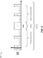
- Fig. 2 is a diagram of an example of a binary multispectral (Fabry-Perot) filter using two quarterwave stacks of high refractive index/low refractive index (HL) pairs.
- Fabry-Perot binary multispectral
- a filter 210 may include a substrate, a first quarterwave stack including alternating high refractive index ( H ) layers and low refractive index (L) layers, a high refractive index spacer, and a second quarterwave stack including alternating high refractive index layers and low refractive index layers.
- the first quarterwave stack and the second quarterwave stack form a first mirror and a second mirror to sandwich the high refractive index spacer.
- the first quarterwave stack and the second quarterwave stack may completely cover the high refractive index spacer.
- the first quarterwave stack and the second quarterwave stack may partially cover the high refractive index spacer.
- filter 210 may include one or more other layers to provide one or more other functionalities.
- filter 210 may include one or more blocker layers to block a particular wavelength of light, one or more anti-reflectance layers, one or more protective layers to reduce environmental degradation of the quarterwave stacks, and/or the like.
- filter 210 may include greater than two quarterwave stacks.
- filter 210 may include a first quarterwave stack and a second quarterwave stack forming a first mirror and a third quarter wave stack and a fourth quarterwave stack forming a second mirror.
- filter 210 may include mirrors formed from three quarterwave stacks, four quarterwave stacks, and/or the like.
- each quarterwave stack may be a same set of materials.
- each quarterwave stack may include a particular high refractive index material and a particular low refractive index material.
- a first quarterwave stack may include a first high refractive index material and a first low refractive index material and a second quarterwave stack may include a second high refractive index material and a second low refractive index material.
- each mirror may include a same quantity of quarterwave stacks.
- a first mirror may include the first quarterwave stack and a second mirror may include the second quarterwave stack.
- the first mirror may include a set of two quarterwave stacks and the second mirror may include a set of three quarterwave stacks.
- a quantity, composition, arrangement, and/or the like of layers and/or quarterwave stacks in filter 210 may be selected to configure a particular bandwidth, angle shift, transmissivity, spectral range, and/or the like for filter 210.
- the high refractive index layers of the first quarterwave stack and/or the second quarterwave stack may each be associated with a refractive index of greater than approximately 3.0, greater than approximately 3.5, greater than approximately 3.6, greater than approximately 3.7, greater than approximately 3.8, greater than approximately 3.9, greater than approximately 4.0, and/or the like.
- the high refractive index layers may be a single material, such as silicon, silicon germanium, germanium, hydrogenated silicon, hydrogenated silicon germanium, hydrogenated germanium, and/or the like.
- the high refractive index layers may include multiple materials, such as a combination of hydrogenated silicon layers and hydrogenated silicon germanium layers.
- the high refractive index layers of the first quarterwave stack and/or the second quarterwave stack may each be associated with a physical thickness of between approximately 40 nm and approximately 300 nm, between approximately 60 nm and approximately 180 nm, between approximately 70 nm and approximately 90 nm, approximately 78 nm, and/or the like.
- the high refractive index layers of the first quarterwave stack and the second quarterwave stack may each be associated with a quarterwave optical thickness of between approximately 75 nm and approximately 500 nm, between approximately 120 nm and approximately 300 nm, between approximately 180 nm and approximately 250 nm, approximately 230 nm, and/or the like.
- Quarterwave optical thickness of a layer corresponds to the physical thickness and refractive index of the layer, as described herein.
- the low refractive index layers of the first quarterwave stack and the second quarterwave stack may each be associated with a refractive index of less than approximately 2.5, less than approximately 2.0, less than approximately 1.5, and/or the like.
- a difference between a first refractive index of the high refractive index layers and a second refractive index of the low refractive index layers may be greater than approximately 1.5, greater than approximately 2.0, greater than approximately 2.5, and/or the like.
- the low refractive index layers may include a set of silicon dioxide (SiO 2 ) layers, a set of aluminum oxide (Al 2 O 3 ) layers, a set of titanium dioxide (TiO 2 ) layers, a set of niobium pentoxide (Nb 2 O 5 ) layers, a set of tantalum pentoxide (Ta 2 O 5 ) layers, a set of magnesium fluoride (MgF 2 ) layers, a set of silicon nitride (S 3 N 4 ) layers, zirconium oxide (ZrOz 2 ), yttrium oxide (Y 2 O 3 ), and/or the like.
- the low refractive index layers of the first quarterwave stack and the second quarterwave stack may each be associated with a range of physical thicknesses based on a wavelength range that is to be covered and a refractive index that of a material that is used. For example, a thickness of approximately 231 nm and/or the like may be used for the low refractive index layers and/or the quarterwave stacks formed therefrom. In some implementations, the low refractive index layers of the first quarterwave stack and the second quarterwave stack may each be associated with a quarterwave optical thickness of approximately 1100 to approximately 2000 nm, approximately 1200 to approximately 1600 nm, approximately 1350 nm, and/or the like.
- the high refractive index spacer layer is associated with a physical thickness of approximately 78 nm, and a quarterwave optical thickness of approximately 1350 nm.
- the high refractive index spacer layer may be a same material as the high refractive index layers, a different material than the high refractive index layers, a combination of a same and a different material, and/or the like.
- a refractive index, a thickness, a quantity, and/or the like of layers of filter 210 may be selected to cause filter 210 to provide a threshold quantity of channels (e.g., at least 32 channels, at least 64 channels, at least 128 channels, and/or the like), a threshold spectral width as described herein, a threshold channel width as described herein, a threshold transmissivity, and/or the like.
- a threshold quantity of channels e.g., at least 32 channels, at least 64 channels, at least 128 channels, and/or the like
- a threshold spectral width as described herein
- a threshold channel width as described herein
- a threshold transmissivity e.g., a threshold transmissivity
- filter 210 may be fabricated using a sputtering procedure.
- filter 210 may be fabricated using a pulsed-magnetron based sputtering procedure to sputter alternating layers on a glass substrate, a silicon substrate, or another type of substrate.
- multiple cathodes may be used for the sputtering procedure, such as a first cathode to sputter silicon and a second cathode to sputter germanium.
- filter 210 may be annealed using one or more annealing procedures, such as a first annealing procedure at a temperature of approximately 280 degrees Celsius or between approximately 200 degrees Celsius and approximately 400 degrees Celsius, a second annealing procedure at a temperature of approximately 320 degrees Celsius or between approximately 250 degrees Celsius and approximately 350 degrees Celsius, and/or the like.
- annealing procedures such as a first annealing procedure at a temperature of approximately 280 degrees Celsius or between approximately 200 degrees Celsius and approximately 400 degrees Celsius, a second annealing procedure at a temperature of approximately 320 degrees Celsius or between approximately 250 degrees Celsius and approximately 350 degrees Celsius, and/or the like.
- the high refractive index spacer layer may include multiple spacer layers of a particular material and of multiple thicknesses selected to form multiple channels. For example, in a first case, the high refractive index spacer layer may be formed using multiple layers to form 64 channels. Similarly, in a second case, the high refractive index spacer layer may be formed using multiple layers to form 128 channels.
- Fig. 2 is provided merely as an example. Other examples are possible and may differ from what was described with regard to Fig. 2 .
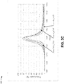
- Figs. 3A-3D are diagrams of example optical characteristics of a binary multispectral (e.g., a Fabry-Perot) filter using one or more selected materials for high refractive index layers, such as a filter 210, described with regard to Fig. 2A .
- a binary multispectral e.g., a Fabry-Perot
- a spectral bandwidth is determined for a channel using a particular material for a high refractive index layer of a binary multispectral filter described herein. For example, for a channel centered at approximately 1350 nm, use of silicon results in a spectral width from approximately 980 nm to approximately 2180 nm at a transmissivity of 50% and a spectral width from approximately 960 nm to approximately 2250 nm at a peak transmissivity of approximately 95%.
- use of silicon germanium results in a spectral width from approximately 975 nm to approximately 2250 nm at a transmissivity of 50% and a spectral width from approximately 955 nm to approximately 2275 nm at a peak transmissivity of approximately 95%.
- use of silicon germanium for high refractive index layers results in an increase to a spectral width, thereby improving performance of the binary multispectral filter.
- germanium results in a reduction of transmissivity at approximately 980 nm to less than approximately 25%, a 50% transmissivity is occurs at 2275 nm, and a peak transmissivity occurs at 2300 nm.
- use of germanium for high refractive index layers results in an increase to a spectral width and/or obviates a need for a blocker to block transmissivity at less than 1000 nm, thereby improving performance of a binary multispectral filter, reducing manufacturing complexity, reducing cost, and/or reducing size relative to use of other filter materials.
- the multispectral filter may be configured for a greater quantity of channels, a greater range of bandwidths, and/or the like, which may improve sensing, such as for object sensing, object recognition, medical device sensing, biometric sensing, and/or the like.
- a spectral bandwidth is determined for a channel at 1800 nm and at an angle of incidence of 0 degrees using a particular material for a high refractive index layer of a binary multispectral filter described herein.
- a peak of approximately 95% transmissivity may be achieved, and a spectral width for 50% transmissivity may extend from 1795 nm to 1835 nm.
- a peak of approximately 95% transmissivity may be achieved, and a spectral width for 50% transmissivity may extend from 1805 nm to 1830 nm.
- a peak of approximately 95% transmissivity may be achieved, and a spectral width for 50% transmissivity may extend from 1810 nm to 1825 nm. In this way, use of hydrogenated germanium may result in a narrower spectral width for a channel, thereby improving filter performance relative to another material selection.
- reducing a spectral width for a single channel may result in reduced interference from other bandwidths when sensing a particular bandwidth for the channel.
- reducing a spectral width for a single channel may enable a greater density of channels for a multispectral filter, thereby enabling improved sensing for a particular device that includes a multispectral filter.
- a spectral bandwidth is determined for a channel at 1800 nm and at an angle of incidence of 20 degrees using a particular material for a high refractive index layer of a binary multispectral filter described herein.
- a peak of approximately 82% transmissivity may be achieved, and a spectral width for 50% transmissivity may extend from 1775 nm to 1815 nm.
- a peak of approximately 78% transmissivity may be achieved, and a spectral width for 50% transmissivity may extend from 1780 nm to 1815 nm.
- a peak of approximately 68% transmissivity may be achieved, and a spectral width for 50% transmissivity may extend from 1785 nm to 1810 nm.
- use of hydrogenated germanium may result in a narrower spectral width for a channel, thereby improving filter performance relative to another material selection.
- use of hydrogenated silicon may result in an improved peak transmissivity at angles of incidence greater than a threshold, which may improve performance of the binary multispectral filter.
- a reduced angle shift as a result of an increase to an angle of incidence, thereby improving filter performance.
- table 1 Table 1 CWL shift AOI Si Ge Si Ge [°] [nm] [nm] [nm] [nm] 0 1818.0 1815.8 0 0 20 1798.1 1799.2 20.0 16.6 30 1773.6 1778.2 44.4 37.6 for a germanium (Ge) based design, relative to a Silicon (Si) based design for a multispectral filter, a center wavelength (CWL) shift value may be reduced at angles of incidence (AOI).
- a center wavelength shift value may be reduced from 20.0 nm to 16.6 nm for germanium based designs relative to silicon based designs, and at an angle of incidence of 30 degrees, a center wavelength shift value may be reduced from 44.4 nm to 37.6 nm.
- some implementations, described herein may reduce interference from light received at a threshold angle of incidence, improve sensing of a particular wavelength of light, and may obviate a need for an aperture to control angle of incidence, thereby reducing a cost, a size, and/or the like of a device that includes a multispectral filter.
- a spectral bandwidth is determined, without accounting for quantum efficiency of a detector, for a 64 channel binary multispectral filter described herein.
- the binary multispectral filter may use hydrogenated germanium as a high refractive index layer and may be associated with a set of 64 channels from 1100 nm to 2000 nm.
- a transmissivity of greater than 95% is achieved for channels at 1650 nm and higher
- a transmissivity of 80% is achieved for channels at 1400 nm and higher
- a transmissivity of 50% is achieved for channels at 1300 nm and higher, etc.
- less than a threshold transmissivity may be achieved using hydrogenated germanium as a high refractive index layer (e.g., less than approximately 70%, less than approximately 50%, less than approximately 30%, less than approximately 20%, and/or the like).
- a plurality of pixels e.g., a plurality of sensor elements of a sensor element array
- the binary multispectral filter may be associated with 5 aligned pixels (e.g., 5 sensor elements) for a channel at 1100 nm to ensure a flat response.
- 5 aligned pixels e.g., 5 sensor elements
- differentiation in a quantity of pixels (e.g., sensor elements) aligned to each channel may ensure a flat response, thereby improving optical performance of an optical device that includes the binary multispectral filter.
- FIGS. 3A-3D are provided merely as examples. Other examples are possible and may differ from what was described with regard to Figs. 3A-3D .
- a binary multispectral filter may be manufactured using a particular set of materials for a high refractive index layer (e.g., silicon germanium, germanium, hydrogenated silicon germanium, hydrogenated germanium, and/or the like). Based on using the particular set of materials, the binary multispectral filter may be associated with improved spectral width, reduced angle shift, reduced channel width, and/or the like relative to other materials, thereby improving sensing for an optical system that includes the binary multispectral filter.
- a particular set of materials for a high refractive index layer e.g., silicon germanium, germanium, hydrogenated silicon germanium, hydrogenated germanium, and/or the like.
- satisfying a threshold may refer to a value being greater than the threshold, more than the threshold, higher than the threshold, greater than or equal to the threshold, less than the threshold, fewer than the threshold, lower than the threshold, less than or equal to the threshold, equal to the threshold, etc.
Landscapes
- Physics & Mathematics (AREA)
- General Physics & Mathematics (AREA)
- Optics & Photonics (AREA)
- Spectroscopy & Molecular Physics (AREA)
- Optical Filters (AREA)
Applications Claiming Priority (1)
| Application Number | Priority Date | Filing Date | Title |
|---|---|---|---|
| US16/049,391 US11143803B2 (en) | 2018-07-30 | 2018-07-30 | Multispectral filter |
Publications (2)
| Publication Number | Publication Date |
|---|---|
| EP3605166A2 true EP3605166A2 (de) | 2020-02-05 |
| EP3605166A3 EP3605166A3 (de) | 2020-04-15 |
Family
ID=67438941
Family Applications (1)
| Application Number | Title | Priority Date | Filing Date |
|---|---|---|---|
| EP19188434.5A Pending EP3605166A3 (de) | 2018-07-30 | 2019-07-25 | Multispektraler filter |
Country Status (6)
| Country | Link |
|---|---|
| US (1) | US11143803B2 (de) |
| EP (1) | EP3605166A3 (de) |
| JP (1) | JP2020021052A (de) |
| KR (1) | KR102453499B1 (de) |
| CN (1) | CN110780370A (de) |
| TW (1) | TW202008012A (de) |
Families Citing this family (5)
| Publication number | Priority date | Publication date | Assignee | Title |
|---|---|---|---|---|
| US11650361B2 (en) * | 2018-12-27 | 2023-05-16 | Viavi Solutions Inc. | Optical filter |
| JP7028266B2 (ja) * | 2020-02-11 | 2022-03-02 | 株式会社三洋物産 | 遊技機 |
| JP2021079146A (ja) * | 2021-02-22 | 2021-05-27 | 株式会社三洋物産 | 遊技機 |
| JP7315071B2 (ja) * | 2021-03-03 | 2023-07-26 | 株式会社三洋物産 | 遊技機 |
| TWI897790B (zh) * | 2022-12-30 | 2025-09-11 | 新加坡商光寶科技新加坡私人有限公司 | 多光譜透射濾光片陣列 |
Citations (3)
| Publication number | Priority date | Publication date | Assignee | Title |
|---|---|---|---|---|
| US20030072009A1 (en) * | 2001-08-02 | 2003-04-17 | Domash Lawrence H. | Tunable optical instruments |
| US20180149781A1 (en) * | 2016-11-30 | 2018-05-31 | Viavi Solutions Inc. | Silicon-germanium based optical filter |
| EP3407104A1 (de) * | 2017-05-22 | 2018-11-28 | Viavi Solutions Inc. | Multispektraler filter |
Family Cites Families (22)
| Publication number | Priority date | Publication date | Assignee | Title |
|---|---|---|---|---|
| GB1164352A (en) * | 1967-06-16 | 1969-09-17 | Standard Telephones Cables Ltd | Optical Filters. |
| GB2175016B (en) * | 1985-05-11 | 1990-01-24 | Barr & Stroud Ltd | Optical coating |
| US6301042B1 (en) | 1998-01-15 | 2001-10-09 | Ciena Corporation | Fabry-perot optical filter with chirped dielectric mirrors |
| GB9901858D0 (en) * | 1999-01-29 | 1999-03-17 | Secr Defence | Optical filters |
| WO2000063728A1 (en) | 1999-04-20 | 2000-10-26 | Ciena Corporation | Dual transmission band interference filter |
| US6850366B2 (en) * | 2002-10-09 | 2005-02-01 | Jds Uniphase Corporation | Multi-cavity optical filter |
| TWI298582B (en) | 2002-10-25 | 2008-07-01 | Hon Hai Prec Ind Co Ltd | Thin film filter for dense wavelength division multiplexing |
| CN1306288C (zh) | 2005-04-27 | 2007-03-21 | 中国科学院上海技术物理研究所 | 具有平整谐振腔层的滤光片列阵 |
| US7521658B2 (en) * | 2005-12-01 | 2009-04-21 | Aptina Imaging Corporation | Pixel having photoconductive layers to absorb different ranges of wavelengths |
| WO2010108086A2 (en) * | 2009-03-20 | 2010-09-23 | Nanolambda, Inc. | Nano-optic filter array based sensor |
| KR20120086196A (ko) * | 2011-01-25 | 2012-08-02 | 광주과학기술원 | 실리콘을 이용한 dbr 구조물 및 그 제조방법 |
| IN2014CN02966A (de) * | 2011-11-04 | 2015-07-03 | Imec | |
| CN108572409B (zh) * | 2013-01-29 | 2022-03-01 | 唯亚威通讯技术有限公司 | 可变滤光器及基于此的波长选择传感器 |
| GB2543655B (en) * | 2013-08-02 | 2017-11-01 | Verifood Ltd | Compact spectrometer comprising a diffuser, filter matrix, lens array and multiple sensor detector |
| CN106233168B (zh) * | 2014-04-10 | 2019-09-17 | 瑞士Csem电子显微技术研发中心 | 红外透射盖板 |
| EP3839585B1 (de) * | 2015-02-18 | 2022-11-09 | Materion Corporation | Optische nahinfrarot-interferenzfilter mit verbesserter übertragung |
| US9960199B2 (en) * | 2015-12-29 | 2018-05-01 | Viavi Solutions Inc. | Dielectric mirror based multispectral filter array |
| US10170509B2 (en) * | 2016-02-12 | 2019-01-01 | Viavi Solutions Inc. | Optical filter array |
| JP2017168822A (ja) | 2016-02-12 | 2017-09-21 | ヴァイアヴィ・ソリューションズ・インコーポレイテッドViavi Solutions Inc. | センサデバイスの製造方法 |
| JP6410203B1 (ja) * | 2017-02-21 | 2018-10-24 | 株式会社ナノルクス | 固体撮像素子及び撮像装置 |
| US10677972B2 (en) | 2017-12-08 | 2020-06-09 | Viavi Solutions Inc. | Multispectral sensor response balancing |
| FR3082322B1 (fr) * | 2018-06-08 | 2020-07-31 | Commissariat A L Energie Atomique Et Aux Energies Alternatives | Capteurs d'images comprenant une matrice de filtres interferentiels |
-
2018
- 2018-07-30 US US16/049,391 patent/US11143803B2/en active Active
-
2019
- 2019-07-04 TW TW108123597A patent/TW202008012A/zh unknown
- 2019-07-09 JP JP2019127828A patent/JP2020021052A/ja active Pending
- 2019-07-25 EP EP19188434.5A patent/EP3605166A3/de active Pending
- 2019-07-29 KR KR1020190092060A patent/KR102453499B1/ko active Active
- 2019-07-29 CN CN201910689420.8A patent/CN110780370A/zh active Pending
Patent Citations (3)
| Publication number | Priority date | Publication date | Assignee | Title |
|---|---|---|---|---|
| US20030072009A1 (en) * | 2001-08-02 | 2003-04-17 | Domash Lawrence H. | Tunable optical instruments |
| US20180149781A1 (en) * | 2016-11-30 | 2018-05-31 | Viavi Solutions Inc. | Silicon-germanium based optical filter |
| EP3407104A1 (de) * | 2017-05-22 | 2018-11-28 | Viavi Solutions Inc. | Multispektraler filter |
Also Published As
| Publication number | Publication date |
|---|---|
| EP3605166A3 (de) | 2020-04-15 |
| US11143803B2 (en) | 2021-10-12 |
| US20200033520A1 (en) | 2020-01-30 |
| KR20200013617A (ko) | 2020-02-07 |
| TW202008012A (zh) | 2020-02-16 |
| JP2020021052A (ja) | 2020-02-06 |
| KR102453499B1 (ko) | 2022-10-11 |
| CN110780370A (zh) | 2020-02-11 |
Similar Documents
| Publication | Publication Date | Title |
|---|---|---|
| US11143803B2 (en) | Multispectral filter | |
| CN108933150B (zh) | 诱导透射滤光器 | |
| US11880054B2 (en) | Multispectral filter | |
| EP3206060B1 (de) | Optische filteranordnung | |
| TWI893644B (zh) | 基於金屬鏡的多光譜濾光片陣列 | |
| KR102200622B1 (ko) | 센서 디바이스를 제작하는 방법 | |
| EP3499279A1 (de) | Optische filter | |
| CN115598756A (zh) | 多带通光学干涉滤光器 | |
| US12044871B2 (en) | Multi-transmission optical filter | |
| CA3002986C (en) | MULTISPECTRAL FILTER WITH MIXED SPACER | |
| HK40014429A (en) | Multispectral filter | |
| CN114114495B (zh) | 一种三通滤光片及其生物识别系统 | |
| HK40115806A (en) | Multispectral filter | |
| HK40062514B (en) | Multispectral filter | |
| HK40081862A (en) | Multi-bandpass optical interference filter | |
| HK40062514A (en) | Multispectral filter | |
| HK1258879B (en) | Mixed spacer multispectral filter | |
| HK40082416A (en) | Low angle shift filter | |
| HK1243224A1 (en) | Method of fabricating a sensor device | |
| HK40002319A (en) | Optical filters | |
| HK1259464B (en) | Multispectral filter | |
| HK40001995A (en) | Multispectral sensor response balancing |
Legal Events
| Date | Code | Title | Description |
|---|---|---|---|
| PUAI | Public reference made under article 153(3) epc to a published international application that has entered the european phase |
Free format text: ORIGINAL CODE: 0009012 |
|
| STAA | Information on the status of an ep patent application or granted ep patent |
Free format text: STATUS: THE APPLICATION HAS BEEN PUBLISHED |
|
| AK | Designated contracting states |
Kind code of ref document: A2 Designated state(s): AL AT BE BG CH CY CZ DE DK EE ES FI FR GB GR HR HU IE IS IT LI LT LU LV MC MK MT NL NO PL PT RO RS SE SI SK SM TR |
|
| AX | Request for extension of the european patent |
Extension state: BA ME |
|
| PUAL | Search report despatched |
Free format text: ORIGINAL CODE: 0009013 |
|
| AK | Designated contracting states |
Kind code of ref document: A3 Designated state(s): AL AT BE BG CH CY CZ DE DK EE ES FI FR GB GR HR HU IE IS IT LI LT LU LV MC MK MT NL NO PL PT RO RS SE SI SK SM TR |
|
| AX | Request for extension of the european patent |
Extension state: BA ME |
|
| RIC1 | Information provided on ipc code assigned before grant |
Ipc: G02B 6/293 20060101ALI20200309BHEP Ipc: G02B 5/28 20060101AFI20200309BHEP |
|
| STAA | Information on the status of an ep patent application or granted ep patent |
Free format text: STATUS: REQUEST FOR EXAMINATION WAS MADE |
|
| 17P | Request for examination filed |
Effective date: 20201008 |
|
| RBV | Designated contracting states (corrected) |
Designated state(s): AL AT BE BG CH CY CZ DE DK EE ES FI FR GB GR HR HU IE IS IT LI LT LU LV MC MK MT NL NO PL PT RO RS SE SI SK SM TR |
|
| STAA | Information on the status of an ep patent application or granted ep patent |
Free format text: STATUS: EXAMINATION IS IN PROGRESS |
|
| 17Q | First examination report despatched |
Effective date: 20220218 |
|
| RAP3 | Party data changed (applicant data changed or rights of an application transferred) |
Owner name: VIAVI SOLUTIONS INC. |
|
| P01 | Opt-out of the competence of the unified patent court (upc) registered |
Effective date: 20230530 |
|
| GRAP | Despatch of communication of intention to grant a patent |
Free format text: ORIGINAL CODE: EPIDOSNIGR1 |
|
| STAA | Information on the status of an ep patent application or granted ep patent |
Free format text: STATUS: GRANT OF PATENT IS INTENDED |
|
| INTG | Intention to grant announced |
Effective date: 20260522 |