EP3598204A2 - Micro-optical system for forming visual images with kinematic movement effects - Google Patents
Micro-optical system for forming visual images with kinematic movement effects Download PDFInfo
- Publication number
- EP3598204A2 EP3598204A2 EP18768308.1A EP18768308A EP3598204A2 EP 3598204 A2 EP3598204 A2 EP 3598204A2 EP 18768308 A EP18768308 A EP 18768308A EP 3598204 A2 EP3598204 A2 EP 3598204A2
- Authority
- EP
- European Patent Office
- Prior art keywords
- area
- optical element
- microoptical
- function
- areas
- Prior art date
- Legal status (The legal status is an assumption and is not a legal conclusion. Google has not performed a legal analysis and makes no representation as to the accuracy of the status listed.)
- Granted
Links
Images



Classifications
-
- G—PHYSICS
- G02—OPTICS
- G02B—OPTICAL ELEMENTS, SYSTEMS OR APPARATUS
- G02B3/00—Simple or compound lenses
- G02B3/0006—Arrays
- G02B3/0037—Arrays characterized by the distribution or form of lenses
- G02B3/0056—Arrays characterized by the distribution or form of lenses arranged along two different directions in a plane, e.g. honeycomb arrangement of lenses
-
- B—PERFORMING OPERATIONS; TRANSPORTING
- B42—BOOKBINDING; ALBUMS; FILES; SPECIAL PRINTED MATTER
- B42D—BOOKS; BOOK COVERS; LOOSE LEAVES; PRINTED MATTER CHARACTERISED BY IDENTIFICATION OR SECURITY FEATURES; PRINTED MATTER OF SPECIAL FORMAT OR STYLE NOT OTHERWISE PROVIDED FOR; DEVICES FOR USE THEREWITH AND NOT OTHERWISE PROVIDED FOR; MOVABLE-STRIP WRITING OR READING APPARATUS
- B42D25/00—Information-bearing cards or sheet-like structures characterised by identification or security features; Manufacture thereof
- B42D25/20—Information-bearing cards or sheet-like structures characterised by identification or security features; Manufacture thereof characterised by a particular use or purpose
- B42D25/29—Securities; Bank notes
-
- B—PERFORMING OPERATIONS; TRANSPORTING
- B42—BOOKBINDING; ALBUMS; FILES; SPECIAL PRINTED MATTER
- B42D—BOOKS; BOOK COVERS; LOOSE LEAVES; PRINTED MATTER CHARACTERISED BY IDENTIFICATION OR SECURITY FEATURES; PRINTED MATTER OF SPECIAL FORMAT OR STYLE NOT OTHERWISE PROVIDED FOR; DEVICES FOR USE THEREWITH AND NOT OTHERWISE PROVIDED FOR; MOVABLE-STRIP WRITING OR READING APPARATUS
- B42D25/00—Information-bearing cards or sheet-like structures characterised by identification or security features; Manufacture thereof
- B42D25/30—Identification or security features, e.g. for preventing forgery
- B42D25/324—Reliefs
-
- B—PERFORMING OPERATIONS; TRANSPORTING
- B42—BOOKBINDING; ALBUMS; FILES; SPECIAL PRINTED MATTER
- B42D—BOOKS; BOOK COVERS; LOOSE LEAVES; PRINTED MATTER CHARACTERISED BY IDENTIFICATION OR SECURITY FEATURES; PRINTED MATTER OF SPECIAL FORMAT OR STYLE NOT OTHERWISE PROVIDED FOR; DEVICES FOR USE THEREWITH AND NOT OTHERWISE PROVIDED FOR; MOVABLE-STRIP WRITING OR READING APPARATUS
- B42D25/00—Information-bearing cards or sheet-like structures characterised by identification or security features; Manufacture thereof
- B42D25/30—Identification or security features, e.g. for preventing forgery
- B42D25/328—Diffraction gratings; Holograms
-
- B—PERFORMING OPERATIONS; TRANSPORTING
- B42—BOOKBINDING; ALBUMS; FILES; SPECIAL PRINTED MATTER
- B42D—BOOKS; BOOK COVERS; LOOSE LEAVES; PRINTED MATTER CHARACTERISED BY IDENTIFICATION OR SECURITY FEATURES; PRINTED MATTER OF SPECIAL FORMAT OR STYLE NOT OTHERWISE PROVIDED FOR; DEVICES FOR USE THEREWITH AND NOT OTHERWISE PROVIDED FOR; MOVABLE-STRIP WRITING OR READING APPARATUS
- B42D25/00—Information-bearing cards or sheet-like structures characterised by identification or security features; Manufacture thereof
- B42D25/30—Identification or security features, e.g. for preventing forgery
- B42D25/355—Security threads
-
- G—PHYSICS
- G02—OPTICS
- G02B—OPTICAL ELEMENTS, SYSTEMS OR APPARATUS
- G02B3/00—Simple or compound lenses
- G02B3/02—Simple or compound lenses with non-spherical faces
- G02B3/08—Simple or compound lenses with non-spherical faces with discontinuous faces, e.g. Fresnel lens
-
- G—PHYSICS
- G02—OPTICS
- G02B—OPTICAL ELEMENTS, SYSTEMS OR APPARATUS
- G02B5/00—Optical elements other than lenses
- G02B5/18—Diffraction gratings
- G02B5/1809—Diffraction gratings with pitch less than or comparable to the wavelength
-
- G—PHYSICS
- G02—OPTICS
- G02B—OPTICAL ELEMENTS, SYSTEMS OR APPARATUS
- G02B5/00—Optical elements other than lenses
- G02B5/18—Diffraction gratings
- G02B5/1814—Diffraction gratings structurally combined with one or more further optical elements, e.g. lenses, mirrors, prisms or other diffraction gratings
- G02B5/1819—Plural gratings positioned on the same surface, e.g. array of gratings
-
- G—PHYSICS
- G02—OPTICS
- G02B—OPTICAL ELEMENTS, SYSTEMS OR APPARATUS
- G02B5/00—Optical elements other than lenses
- G02B5/18—Diffraction gratings
- G02B5/1861—Reflection gratings characterised by their structure, e.g. step profile, contours of substrate or grooves, pitch variations, materials
-
- G—PHYSICS
- G02—OPTICS
- G02B—OPTICAL ELEMENTS, SYSTEMS OR APPARATUS
- G02B5/00—Optical elements other than lenses
- G02B5/18—Diffraction gratings
- G02B5/1876—Diffractive Fresnel lenses; Zone plates; Kinoforms
- G02B5/188—Plurality of such optical elements formed in or on a supporting substrate
-
- G—PHYSICS
- G03—PHOTOGRAPHY; CINEMATOGRAPHY; ANALOGOUS TECHNIQUES USING WAVES OTHER THAN OPTICAL WAVES; ELECTROGRAPHY; HOLOGRAPHY
- G03H—HOLOGRAPHIC PROCESSES OR APPARATUS
- G03H1/00—Holographic processes or apparatus using light, infrared or ultraviolet waves for obtaining holograms or for obtaining an image from them; Details peculiar thereto
- G03H1/0005—Adaptation of holography to specific applications
- G03H1/0011—Adaptation of holography to specific applications for security or authentication
-
- G—PHYSICS
- G07—CHECKING-DEVICES
- G07D—HANDLING OF COINS OR VALUABLE PAPERS, e.g. TESTING, SORTING BY DENOMINATIONS, COUNTING, DISPENSING, CHANGING OR DEPOSITING
- G07D7/00—Testing specially adapted to determine the identity or genuineness of valuable papers or for segregating those which are unacceptable, e.g. banknotes that are alien to a currency
- G07D7/003—Testing specially adapted to determine the identity or genuineness of valuable papers or for segregating those which are unacceptable, e.g. banknotes that are alien to a currency using security elements
-
- G—PHYSICS
- G07—CHECKING-DEVICES
- G07D—HANDLING OF COINS OR VALUABLE PAPERS, e.g. TESTING, SORTING BY DENOMINATIONS, COUNTING, DISPENSING, CHANGING OR DEPOSITING
- G07D7/00—Testing specially adapted to determine the identity or genuineness of valuable papers or for segregating those which are unacceptable, e.g. banknotes that are alien to a currency
- G07D7/06—Testing specially adapted to determine the identity or genuineness of valuable papers or for segregating those which are unacceptable, e.g. banknotes that are alien to a currency using wave or particle radiation
- G07D7/12—Visible light, infrared or ultraviolet radiation
-
- G—PHYSICS
- G07—CHECKING-DEVICES
- G07D—HANDLING OF COINS OR VALUABLE PAPERS, e.g. TESTING, SORTING BY DENOMINATIONS, COUNTING, DISPENSING, CHANGING OR DEPOSITING
- G07D7/00—Testing specially adapted to determine the identity or genuineness of valuable papers or for segregating those which are unacceptable, e.g. banknotes that are alien to a currency
- G07D7/20—Testing patterns thereon
- G07D7/202—Testing patterns thereon using pattern matching
- G07D7/207—Matching patterns that are created by the interaction of two or more layers, e.g. moiré patterns
-
- G—PHYSICS
- G03—PHOTOGRAPHY; CINEMATOGRAPHY; ANALOGOUS TECHNIQUES USING WAVES OTHER THAN OPTICAL WAVES; ELECTROGRAPHY; HOLOGRAPHY
- G03H—HOLOGRAPHIC PROCESSES OR APPARATUS
- G03H1/00—Holographic processes or apparatus using light, infrared or ultraviolet waves for obtaining holograms or for obtaining an image from them; Details peculiar thereto
- G03H1/22—Processes or apparatus for obtaining an optical image from holograms
- G03H1/2202—Reconstruction geometries or arrangements
- G03H2001/2223—Particular relationship between light source, hologram and observer
Definitions
- microoptical system of the formation of visual images with kinematic effects of motion claimed as the invention belongs primarily to the type of devices used to establish the authenticity of products and can be efficiently used for protecting bank notes, securities, documents, plastic cards, and excise stamps.
- patent of invention EA017394(B1 )
- the effects of kinematic motion of fragments are formed by off-axis Fresnel lenses.
- the microoptical system described in patent of invention EA017394(B1 )
- the observer sees an image made up of dots. Every dot of the image is formed by an off-axis Fresnel lens with the preferred size ranging from 0.5 to 1.5 mm.
- the image may consist of digits, letters, or symbols.
- the purpose of this invention is to extend, compared to the prototype, the capabilities of visual control to holographic threads with widths smaller than 5 mm.
- Aim of the present invention is to extend the range of angles where kinematic effects of the motion of image fragments are observed when the optical element is tilted, and also to improve the protection of microoptical systems against counterfeit and limit the number of technologies that allow synthesizing the said visual effect.
- the designated task of obtaining the designated technical result is achieved in the claimed microoptical system of the formation of visual images as per claim 1, which consists of flat diffractive optical element whose domain Q has the form of rectangle Ixl ⁇ L x /2
- Function ⁇ (y) is a periodic extension of function ⁇ (y) defined over interval
- the microoptical system When the microoptical system is illuminated by a point light source then at diffraction angles smaller than 60° the observer sees over the entire area Q of the optical element an image consisting of black and white stripes, which changes if the optical element is tilted right/left within the tilt-angle interval -15° ⁇ ⁇ ⁇ 15°.
- the kinematic effect of motion consists in the motion of black and white stripes when the optical element is tilted up/down within the tilt-angle interval -30° ⁇ ⁇ ⁇ 30°.
- the microoptical system as per claim 2 differs from the microoptical system as per claim 1 in that the area Q of the optical element where phase function ⁇ (x,y) is equal to zero is filled with diffraction gratings of various orientations and periods, which do not exceed 0.6 microns.
- the microoptical system is illuminated by a point light source at diffraction angles smaller than 60° the observer sees over the entire Q area an image consisting of black and white stripes. Which does not change when the optical element is turned right/left within the tilt angle interval -15° ⁇ ⁇ ⁇ 15°.
- the kinematic effect of motion consists in the motion of black and white stripes when the optical element is tilted up/down within the tilt angle interval -30° ⁇ ⁇ ⁇ 30°. At diffraction angles greater than 60° the observer sees another color image.
- the microoptical system as per claim 3 is a flat reflecting diffractive optical element with area Q in the form of a rectangle, Ixl ⁇ L x /2,
- Area Q contains two special non-overlapping subareas: area Q 1 consisting of points (x,y) of area Q with positive x coordinates, and area Q 2 consisting of points (x,y) of area Q with negative x coordinates.
- Function ⁇ (y) defined over the entire area Q is the periodic extension of function ⁇ (y) defined on the interval lyl ⁇ T ⁇ /2 so that ⁇ (y) equals 1 if
- T ⁇ and ⁇ are the given parameters such that ⁇ /T ⁇ ⁇ 1 ⁇ 2.
- the period T ⁇ of Fresnel lenses along the Oy axis, which is equal to T ⁇ L y /M, differs from period T ⁇ by no more than 5%.
- the microoptical system When the microoptical system is illuminated by a point light source at diffraction angles smaller than 60° the observer sees in areas Q 1 and Q 2 images made up of black and white stripes, which do not change when the optical element is turned right/left within the tilt angle interval -15° ⁇ ⁇ ⁇ 15°.
- the kinematic effect consists in the motion of black and white stripes when the optical element is tilted up/down in the tilt angle interval -30° ⁇ ⁇ ⁇ 30°, and black and white stripes in areas Q 1 and Q 2 move in opposite directions.
- the microoptical system as per claim 4 differs from the microoptical system as per claim 3 in that the area Q of the optical element where phase function ⁇ (x,y) is equal to zero is filled with diffraction gratings of various orientations and periods, which do not exceed 0.6 microns.
- the microoptical system is illuminated by a point light source at diffraction angles smaller than 60° the observer sees in areas Q 1 and Q 2 images consisting of black and white stripes, which do not change if the optical element is turned right/left within the turn angle interval -15° ⁇ ⁇ ⁇ 15°.
- the kinematic effect of consists in the motion of black and white stripes when the optical element is tilted up/down within the tilt angle interval -30° ⁇ ⁇ ⁇ 30°, and the stripes in areas Q 1 and Q 2 move in opposite directions. At diffraction angles greater than 60° the observer sees a different image.
- the microoptical system as per claim 5 is a flat reflecting diffractive optical element with area Q in the form of a rectangle, Ixl ⁇ L x /2,
- Area Q contains two special non-overlapping subareas: area Q 1 consisting of points (x,y) of area Q with positive x coordinates, and area Q 2 consisting of points (x,y) of area Q with negative x coordinates.
- Function ⁇ 1 (y) defined over area Q 1 is the periodic extension of function ⁇ 1 (y) defined on the interval lyl ⁇ T ⁇ 1 /2 so that ⁇ 1 (y) equals 1 if
- Function ⁇ 2 (y) defined over area Q 2 is the periodic extension of function ⁇ 2 (y) defined on the interval
- T ⁇ 1 , T ⁇ 2 , ⁇ 1 and ⁇ 2 are the given parameters such that ⁇ 1 /T ⁇ 1 ⁇ 1 ⁇ 2 and ⁇ 2 /T ⁇ 2 ⁇ 1 ⁇ 2.
- the period T ⁇ of Fresnel lenses along the Oy axis, which is equal to T ⁇ L y /M, differs from the periods T ⁇ 1 and T ⁇ 2 by no more than 5%.
- the microoptical system When the microoptical system is illuminated by a point light source at diffraction angles smaller than 60° the observer sees in areas Q 1 and Q 2 images made up of black and white stripes, which do not change when the optical element is turned right/left within the tilt angle interval -15° ⁇ ⁇ ⁇ 15°.
- the kinematic effect consists in the motion of black and white stripes when the optical element is tilted up/down in the tilt angle interval -30° ⁇ ⁇ ⁇ 30°, and black and white stripes in areas Q 1 and Q 2 move in opposite directions.
- the microoptical system as per claim 6 differs from the microoptical system as per claim 5 in that the area Q of the optical element where phase function ⁇ (x,y) is equal to zero is filled with diffraction gratings of various orientations and periods, which do not exceed 0.6 microns.
- the microoptical system is illuminated by a point light source at diffraction angles smaller than 60° the observer sees in areas Q 1 and Q 2 images consisting of black and white stripes, which do not change if the optical element is turned right/left within the turn angle interval -15° ⁇ ⁇ ⁇ 15°.
- the kinematic effect consists in the motion of black and white stripes when the optical element is tilted up/down in the tilt angle interval -30° ⁇ ⁇ ⁇ 30°, and black and white stripes in areas Q 1 and Q 2 move in opposite directions. In the case of diffraction angles greater than 60° the observer sees a different color image.
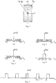
- Fig. 1 shows the domain where the optical element is defined
- Fig. 2 shows the scheme of the partition of the optical element into elementary areas Q ij
- Fig. 3 shows the structure of the axial Fresnel lens in area Q ij
- Fig. 4 shows the phase functions ⁇ + (y) and ⁇ - (y) of the axial Fresnel lenses
- Fig. 5 shows the binary version of the phase function ⁇ (y) of the axial Fresnel lens
- Fig. 6 shows the plot of function ⁇ (y)
- Fig. 7 shows the plot of function ⁇ (y);
- Fig. 1 shows the domain where the optical element is defined
- Fig. 2 shows the scheme of the partition of the optical element into elementary areas Q ij
- Fig. 3 shows the structure of the axial Fresnel lens in area Q ij
- Fig. 4 shows the phase functions ⁇ + (y) and ⁇ - (y) of the axial Fresnel lenses
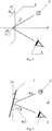
- Fig. 8 shows schematically the mutual positions of the light source and the observer with respect to the microoptical system
- Fig. 9 shows the scheme of observation of the microoptical system in the case where the optical element is tilted up/down by angle ⁇
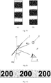
- Fig. 10 shows the variants of the images formed by the microoptical system as per claims 1 and 2 for two different diffraction angles smaller than 60°
- Fig. 11 shows the scheme of observation of the microoptical system in the case of diffraction angles ⁇ > 60
- Fig. 12 shows the variant of the color image seen by the observer at diffraction angles greater than 60°
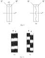
- Fig. 13 shows the variants of the partitioning of the optical element Q into areas Q 1 Q 2 ;
- Fig. 9 shows schematically the mutual positions of the light source and the observer with respect to the microoptical system
- Fig. 9 shows the scheme of observation of the microoptical system in the case where the optical element is tilted up/down by angle ⁇
- Fig. 10 shows
- Fig. 14 shows variants of images formed by the microoptical system as per claims 3 - 6 at diffraction angles smaller than 60°;
- Fig. 15 shows a fragment of the structure of the microrelief of the microoptical system as per claim 4;
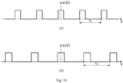
- Fig. 16 shows the plots of functions ⁇ 1 (y) and ⁇ 2 (y) as per claims 5 and 6;
- Fig. 17 shows a fragment of the structure of the microrelief of the microoptical system as per claim 6;
- Fig. 18 shows an example of the partition of a 4.5 mm wide security thread into areas Q 1 and Q 2 ;
- Fig. 19 shows images seen by the observer at diffraction angles smaller than 60° (a) and greater than 60° (b) for a 4.5 mm wide security thread.
- the microoptical system claimed in this invention is a flat optical phase element consisting of multilevel diffraction elements - axial Fresnel lenses and diffraction gratings.
- Fig. 1 shows area Q where the optical element as per claims 1-6 is defined. Area Q has the form of an L x ⁇ L y rectangle centered on the origin of the Cartesian coordinate system Oxy.
- Fig. 2 shows the partition scheme of the optical element into elementary areas Q ij . The center of each elementary area Q ij is located at the point with the coordinates (x i ,y j ). The sizes of the elementary areas do not exceed 250 microns.
- the rectangle is elongate along the Oy axis, i.e., L y >L x .
- the microoptical system is formed using axial Fresnel lenses.
- Fig. 3 shows schematically the mutual positions of the Fresnel lenses in elementary areas Q ij .
- the solid lines show the contours of the phase function.
- We use the functions ⁇ + (x,y) and ⁇ - (x,y) defined by the formula ⁇ (x,y) C ⁇ (x 2 +y 2 ), where C is the given parameter as the phase functions for concave and convex lenses, respectively.
- the phase functions shown in Fig. 4 correspond to multilevel phase elements ( A.V. Goncharsky and A.A. Goncharsky, Computer Optics and Computer Holography, Moscow: Moscow University Press, 2004, ISBN 5-211-04902-0 ). This is the preferred variant for the formation of microoptical systems in accordance with the claimed invention.
- Fig. 5 shows the variant of a binary phase element. Unlike the phase function of a multilevel flat optical element the phase function of a binary optical element takes only two values. Only multilevel axial Fresnel lenses with a parabolic function are used in all claims.
- Phase function ⁇ (x,y) uniquely determines the microrelief of the flat optical element in area Q. Given the phase function it is possible to compute the depth of the microrelief at each point (x, y) of area Q.
- Fig. 8 shows schematically the arrangement of microoptical system 1 relative to the Oxy plane.
- the microoptical system is illuminated by point light source 2 located in the Oyz plane.
- the optical element may turn about the Ox axis by angle ⁇ . Let us denote the turn angle of the optical element about the Oy axis as ⁇ .
- the eye of the observer is located in the Oyz plane.
- the optical element is turned up/down about the Ox axis and left/right about the Oy axis.
- Fig. 9 shows the scheme of observation for microoptical system 1 in the range of diffraction angles smaller than 60°.
- Diffraction angle ⁇ is measured as the angle between the zero order of diffraction denoted as ray R2 in Fig. 9 and the direction toward observer's eye 3.
- the direction of ray R2 coincides with the direction of the ray from light source 2 reflected from the optical element (ray R1) if the phase function of the optical element is constant, i.e., if the optical element is a mirror.
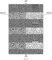
- Fig. 10 shows two images seen by the observer at different angles ⁇ smaller than 60°.
- the image at diffraction angles smaller than 60° is formed via fragments of axial Fresnel lenses with a parabolic phase function.
- the size of the outermost Fresnel zones is an important parameter characterizing flat axial Fresnel lenses. In the preferred version of the invention the size of the outermost Fresnel zones does not exceed 1.2 microns. Because the size of rectangular Fresnel lenses does not exceed 250 microns and the size of the outermost Fresnel zones does not exceed 1.2 microns the lens produces a horizontally wide directivity diagram of the light reflected from the microoptical system.
- Fresnel lenses form an image consisting of horizontal black and white stripes, which does not change if the optical element is turned about the Oy axis left/right by angles ⁇ lying within the ⁇ 15° interval.
- the kinematic effect consists in the motion of black-and-white stripes when the microoptical system is tilted up/down by angles within the ⁇ 30° interval.
- Fresnel lenses cannot be seen by human eye because their size does not exceed 250 microns, which makes the claimed invention essentially different from the prototype where the diameter of Fresnel lenses in the preferred variant ranges from 0.5 to 1.5 mm. the chosen parameters make it possible to form an image, which, unlike that of the prototype, does not consist of isolated points but has the form of solid bright black and white strips, which move in the vertical direction when the optical element is tilted up/down.
- An essential difference from the prototype is that the claimed microoptical system uses multilevel optical elements as Fresnel lenses. It because of the use of multilevel optical elements that the behavior of the motion of stripes does not change across the zero order of diffraction, which corresponds to the transition from positive angles of the tilt of the optical element, ⁇ > 0, to negative angles ⁇ ⁇ 0.
- the microoptical system as per claim 2 differs from the microoptical system as per claim 1 in that area Q of the optical element where the phase function ⁇ (x,y) equals zero is filled with diffraction gratings of various orientations and various periods, which do not exceed 0.6 microns.
- area Q of the optical element where the phase function ⁇ (x,y) equals zero is filled with diffraction gratings of various orientations and various periods, which do not exceed 0.6 microns.
- Fig. 11 shows the observation scheme of the microoptical system art large diffraction angles ⁇ > 60°.
- diffraction angle ⁇ is measured as the angle between the direction toward the observer 3 and the zero order of diffraction R2.
- Figs. 9 and 11 differ only by the value of angle ⁇ .
- Large tilts of the optical element correspond to large angles ⁇ and hence to large diffraction angles ⁇ .
- the parameters of the microrelief of the microoptical system are chosen so that at diffraction angles greater than 60° the image is formed by diffraction gratings.
- the sizes of diffraction gratings do not exceed 200 microns and therefore grating fragments cannot be seen by the observer.
- Fig. 12 shows a variant of such a color image in representative colors. Black and gray correspond to green and red color, respectively.
- area Q is subdivided inti two areas Q 1 and Q 2 as shown in Fig. 13 .
- the boundary between areas Q 1 and Q 2 may have the form of both a straight line as shown in Fig. 13(a) and of an undulating line as shown in Fig. 13(b) .
- the microoptical system as per claim 3 has optical-element area subdivided into areas Q 1 and Q 2 .
- phase functions ⁇ + ij (x,y) in area Q 1 and ⁇ - ij (x,y) in area Q 2 differ only in sign.
- Functions ⁇ (y) coincide in areas Q 1 and Q 2 .
- Function ⁇ (y) which is defined over the entire area Q, is the periodic extension of function ⁇ (y) defined on the interval lyl ⁇ T ⁇ /2.
- Function ⁇ (y) equals 1 if lyl ⁇ ⁇ /2 and equals 0 if
- Fig. 14 shows the variants of the images of the microoptical system as per claims 3 - 6 at various diffraction angles smaller than 60°.
- the microoptical system as per claim 4 differs in that area Q of the optical element where phase function ⁇ (x,y) equals zero is filled with diffraction gratings of various orientations and various periods, which do not exceed 0.6 microns.
- Fig. 15 shows a fragment of the microstructure of the microoptical system as per claim 4.
- the presented fragment has the size of 400 microns along the Ox axis and 608.4 microns along the Oy axis.
- the depth of the microrelief at point (x,y) is proportional to darkening at that point.
- the microoptical system as per claim 5 has area Q of the optical element subdivided into areas Q 1 and Q 2 . Each of the areas Q 1 and Q 2 is subdivided into elementary areas Q 1 ij and Q 2 ij .
- phase functions ⁇ ij (x,y) in areas Q 1 and Q 2 coincide.
- Functions ⁇ 1 (y) and ⁇ 2 (y) in areas Q 1 and Q 2 are different.
- Functions ⁇ 1 (y) and ⁇ 2 (y) are chosen as follows.
- Function ⁇ 1 (y) defined in area Q 1 is the periodic extension of function ⁇ 1 (y) defined on the
- Function ⁇ 2 (y) defined in area Q 2 is the periodic extension of function ⁇ 2 ( Y ) defined on the
- the parameters T ⁇ 1 , T ⁇ 2 , ⁇ 1' and ⁇ 2 are given parameters such that ⁇ 1 /T ⁇ 1 ⁇ 1 ⁇ 2, ⁇ 2 /T ⁇ 2 ⁇ 1 ⁇ 2.
- T ⁇ 1 ⁇ T ⁇ ⁇ T ⁇ 2 or T ⁇ 2 ⁇ T ⁇ ⁇ T ⁇ 1 - is satisfied.
- Fig. 16 shows plots of functions ⁇ 1 (y) and ⁇ 2 (y).
- Fig. 17 shows a fragment of the microstructure of the microoptical system as per claim 6.
- the phase functions ⁇ ij (x,y) in areas Q 1 and Q 2 coincide, but functions ⁇ 1 (y) and ⁇ 2 (y) are different.
- the depth of the microrelief at point (x,y) is proportional to darkening at that point.
- Fig. 18 shows another variant of the partition of the security thread into areas Q 1 and Q 2 . Such a variant can be efficiently used if the width of the thread is greater than 4 mm.
- Fig. 19 shows the images seen by the observer at diffraction angles smaller than 60° (a) and greater than 60° (b) for a 4.5 mm wide security thread. The effect of the motion of black and white stripes at diffraction angles smaller than 60° is easy to control visually. At diffraction angles greater than 60° the observer sees another color image over the entire area of the optical element.
- Microoptical systems proposed in the claimed invention are made using electron-beam technology. Electron-beam lithography provides very high resolution (0.1 microns or better) and ensures the required accuracy of the production of the microrelief - about 20 nanometers. Currently, several hundred companies produce security holograms. Practically all these companies use optical technologies to record the originals of security features. Optical methods of the synthesis of originals include the technologies KineMax, Kinegram, etc. ( van Renesse, Rudolf L, Optical Document Security, 3rd ed.
- microoptical systems were made in the form of a 2 mm, 3 mm and 4.5 mm wide reflecting holographic thread for protecting bank notes and securities.
- the size of Q ij rectangles was about 100x200 microns.
- the minimal size of the outermost Fresnel zone is of about 1.2 microns.
- the number of Fresnel zones is on the order of 50.
- the size of the central zone is about 10 microns.
- Figs. 9 and 11 show the scheme of observation of the microoptical system at diffraction angles ⁇ ⁇ 60° and ⁇ > 60°, respectively.
- diffraction gratings with the periods of 0.45 and 0.55 micron were used.
- the size of the fragments pf diffraction gratings is 20 microns.
- a microoptical system was made in the form of a 2 mm wide holographic security thread.
- Fig. 2 shows the scheme of the partitioning of the optical element into elementary areas Q ij .
- the phase function ⁇ + ij (x,y) was used for the formation of Fresnel lenses.
- Fig. 12 shows the color image seen at large diffraction angles (greater than 60°).
- Fig. 10 shows the monochrome image seen at diffraction angles smaller than 60°.
- the monochrome image consists of black and white stripes, which move when the holographic thread is tilted up/down.
- a microoptical system was made in the form of a 3 mm wide holographic security thread.
- Fig. 2 shows the scheme of the partitioning of the optical element into areas Q 1 and Q 2 .
- the phase functions ⁇ + ij (x,y) and ⁇ - ij (x,y) were used for areas Q 1 and Q 2 , respectively.
- Fig. 13(a) shows the color image seen at large diffraction angles (greater than 60°).
- Fig. 12 shows the monochrome image seen at diffraction angles smaller than 60°.
- the monochrome image consists of black and white stripes, which move toward each other when the holographic thread is tilted up/down.
- a microoptical system was made in the form of a 3 mm wide holographic security thread.
- Fig. 13(b) shows the scheme of the partitioning of the optical element into areas Q 1 and Q 2 .
- the phase functions ⁇ + ij (x,y) was used for areas Q 1 and Q 2 , respectively.
- Fig. 12 shows the color image seen at large diffraction angles (greater than 60°).
- Fig. 14 shows the monochrome image seen at diffraction angles smaller than 60°.
- the monochrome image consists of black and white stripes, which move toward each other when the holographic thread is tilted up/down.
- a microoptical system was made in the form of a 4.5 mm wide holographic security thread.
- Fig. 18 shows the scheme of the partitioning of the optical element Q into areas Q 1 and Q 2 .
- the phase functions ⁇ + ij (x,y) and ⁇ - ij (x,y) were used for areas Q 1 and Q 2 , respectively.
- Fig. 19(b) shows the color image seen at large diffraction angles greater than 60°.
- Fig. 19(a) shows the monochrome image seen at diffraction angles smaller than 60°.
- Visual images are easy to control.
- Microoptical systems are securely protected against counterfeit.
- Microoptical systems claimed in the invention can be used to protect bank notes, securities, documents, excise stamps, and plastic cards.
Landscapes
- Physics & Mathematics (AREA)
- General Physics & Mathematics (AREA)
- Optics & Photonics (AREA)
- Engineering & Computer Science (AREA)
- Health & Medical Sciences (AREA)
- Computer Security & Cryptography (AREA)
- General Health & Medical Sciences (AREA)
- Toxicology (AREA)
- Business, Economics & Management (AREA)
- Accounting & Taxation (AREA)
- Finance (AREA)
- Computer Vision & Pattern Recognition (AREA)
- Diffracting Gratings Or Hologram Optical Elements (AREA)
- Inspection Of Paper Currency And Valuable Securities (AREA)
- Credit Cards Or The Like (AREA)
Abstract
Description
- Currently, various protection technologies are used to protect bank notes, securities, documents, and plastic cards against counterfeit. These include water marks, windowed threads, holograms, embedded LED elements varying the polarization of the incident light, latent images, etc. (van Renesse, Rudolf L, Optical Document Security, 3rd ed. British Library Cataloguing in Publication Data, 2005, ISBN 1-58053-258-6, van Renesse, Rudolf L, Optical Document Security, 2nd ed. British Library Cataloguing in Publication Data, 1998, ISBN 0-89006-982-4).
- The microoptical system of the formation of visual images with kinematic effects of motion claimed as the invention belongs primarily to the type of devices used to establish the authenticity of products and can be efficiently used for protecting bank notes, securities, documents, plastic cards, and excise stamps.
- The closest patent to the claimed invention (prototype) in terms of the combination of features is patent of invention (
EA017394(B1 EA017394(B1 RU127208 EA017394(B1 - The purpose of this invention is to extend, compared to the prototype, the capabilities of visual control to holographic threads with widths smaller than 5 mm. Currently, the overwhelming majority of threads used to protect bank notes and securities have widths smaller than 5 mm. Aim of the present invention is to extend the range of angles where kinematic effects of the motion of image fragments are observed when the optical element is tilted, and also to improve the protection of microoptical systems against counterfeit and limit the number of technologies that allow synthesizing the said visual effect.
- The designated task of obtaining the designated technical result is achieved in the claimed microoptical system of the formation of visual images as per
claim 1, which consists of flat diffractive optical element whose domain Q has the form of rectangle Ixl ≤ Lx/2 |y| ≤ Ly/2 placed on flat base. Domain Q is subdivided into elementary areas Qij, each with a size no greater than 250 microns and centered on points (xi,yj), i = 1 ... N, j = 1 ... M. For each area Qij a flat optical element with phase function Φ(x,y), which at point of each elementary area Qij is calculated by formula Φ(x,y) = ϕij(x,y) · ψ(y), i = 1 ... N, j = 1 ... M, is computed and manufactured. Function ϕij(x,y) has the form of the phase function of an off-axis Fresnel lens centered on point (xi,yj), and computed by the formula ϕij(x,y) = C[(x-xi)2+(y-yj)2], where C is the given parameter. Function ψ(y) is a periodic extension of functionψ (y) defined over interval |y| ≤ Tψ/2 so thatψ (y) equals 1 if |y| ≤ Δ/2, and 0 if |y| > Δ/2. The quantities Tψ and Δ are specified parameters such that Δ/Tψ ≤ ½, and the period Tϕ of Fresnel lenses along the Oy axis, which is equal to Tϕ = Ly/M, differs from the period Tψ by no more than 5%. When the microoptical system is illuminated by a point light source then at diffraction angles smaller than 60° the observer sees over the entire area Q of the optical element an image consisting of black and white stripes, which changes if the optical element is tilted right/left within the tilt-angle interval -15°< β < 15°. The kinematic effect of motion consists in the motion of black and white stripes when the optical element is tilted up/down within the tilt-angle interval -30°< α < 30°. - The microoptical system as per
claim 2 differs from the microoptical system as perclaim 1 in that the area Q of the optical element where phase function Φ(x,y) is equal to zero is filled with diffraction gratings of various orientations and periods, which do not exceed 0.6 microns. When the microoptical system is illuminated by a point light source at diffraction angles smaller than 60° the observer sees over the entire Q area an image consisting of black and white stripes. Which does not change when the optical element is turned right/left within the tilt angle interval -15°< β < 15°. The kinematic effect of motion consists in the motion of black and white stripes when the optical element is tilted up/down within the tilt angle interval -30°< α < 30°. At diffraction angles greater than 60° the observer sees another color image. - The microoptical system as per
claim 3 is a flat reflecting diffractive optical element with area Q in the form of a rectangle, Ixl ≤ Lx/2, |y| ≤ Ly/2. Area Q contains two special non-overlapping subareas: area Q1 consisting of points (x,y) of area Q with positive x coordinates, and area Q2 consisting of points (x,y) of area Q with negative x coordinates. Each of the areas Q1 and Q2 is subdivided into elementary areas Q1 ij and Q2 ij with the sizes no greater than 250 microns centered on points (xi,yj), i = 1 ... N/2, j = 1 ... M. For each area Q1 ij a flat optical element is calculated and manufactured with phase function Φ(x,y), which at point (x,y) of elementary area Q1 ij is computed by formula Φ(x,y) = ϕ+ ij(x,y) · ψ(y), i = 1 ... N/2, j = 1 ... M, where ϕ+ ij(x,y) is the phase function of a concave axial Fresnel lens centered on point (xi,yj) and computed by formula ϕ+ ij(x,y) = C[(x-xi)2+(y-yj)2], where C is a given positive parameter. For each area Q1 ij a flat optical element is calculated and manufactured with phase function Φ(x,y), which st point (x,y) of elementary area Q2 ij is computed by formula Φ(x,y) = ϕ- ij(x,y) · ψ(y), i = 1 ... N/2, j = 1 ... M, where ϕ- ij(x,y) is the phase function of a convex Fresnel lens centered on point (xi,yj) computed by formula ϕ- ij(x,y) = C[(x-xi)2+(y-yj)2], where C is a given negative parameter. Function ψ(y) defined over the entire area Q is the periodic extension of functionψ (y) defined on the interval lyl ≤ Tψ/2 so thatψ (y) equals 1 if |y| ≤ Δ/2 and equals 0 if |y| > Δ/2. Here Tψ and Δ are the given parameters such that Δ/Tψ ≤ ½. The period Tϕ of Fresnel lenses along the Oy axis, which is equal to Tϕ = Ly/M, differs from period Tψ by no more than 5%. When the microoptical system is illuminated by a point light source at diffraction angles smaller than 60° the observer sees in areas Q1 and Q2 images made up of black and white stripes, which do not change when the optical element is turned right/left within the tilt angle interval -15°< β < 15°. The kinematic effect consists in the motion of black and white stripes when the optical element is tilted up/down in the tilt angle interval -30°< α < 30°, and black and white stripes in areas Q1 and Q2 move in opposite directions. - The microoptical system as per claim 4 differs from the microoptical system as per
claim 3 in that the area Q of the optical element where phase function Φ(x,y) is equal to zero is filled with diffraction gratings of various orientations and periods, which do not exceed 0.6 microns. When the microoptical system is illuminated by a point light source at diffraction angles smaller than 60° the observer sees in areas Q1 and Q2 images consisting of black and white stripes, which do not change if the optical element is turned right/left within the turn angle interval -15°< β < 15°. The kinematic effect of consists in the motion of black and white stripes when the optical element is tilted up/down within the tilt angle interval -30°< α < 30°, and the stripes in areas Q1 and Q2 move in opposite directions. At diffraction angles greater than 60° the observer sees a different image. - The microoptical system as per claim 5 is a flat reflecting diffractive optical element with area Q in the form of a rectangle, Ixl ≤ Lx/2, |y| ≤ Ly/2. Area Q contains two special non-overlapping subareas: area Q1 consisting of points (x,y) of area Q with positive x coordinates, and area Q2 consisting of points (x,y) of area Q with negative x coordinates. Each of the areas Q1 and Q2 is subdivided into elementary areas Q1 ij and Q2 ij with the sizes no greater than 250 microns centered on points (xi,yj), i = 1 ... N/2, j = 1 ... M. For each area Q1 ij a flat optical element is calculated and manufactured with phase function Φ(x,y), which at point (x,y) of elementary area Q1 ij is computed by formula Φ(x,y) = ϕij(x,y) · ψ1(y), i = 1 ... N/2, j = 1 ... M. For each area Q1 ij a flat optical element is calculated and manufactured with phase function Φ(x,y), which at point (x,y) of elementary area Q2 ij is computed by formula Φ(x,y) = ϕij(x,y) · ψ2(y), i = 1 ... N/2, j = 1 ... M. Here ϕij(x,y) is the phase function of an axial Fresnel lens centered on point (xi,yj) computed by formula ϕ- ij(x,y) = C[(x-xi)2+(y-yj)2], where C is a given parameter. Function ψ1(y) defined over area Q1 is the periodic extension of function
ψ 1(y) defined on the interval lyl ≤ Tψ1/2 so thatψ 1(y) equals 1 if |y| ≤ Δ1/2 and equals 0 if |y| > Δ1/2. Function ψ2(y) defined over area Q2 is the periodic extension of functionψ 2(y) defined on the interval |y| ≤ Tψ2/2 so that ψ2(y) equals 1 if |y| ≤ Δ2/2 and equals 0 if |y| > Δ2/2. Here Tψ1, Tψ2, Δ1 and Δ2 are the given parameters such that Δ1/Tψ1 ≤ ½ and Δ2/Tψ2 ≤ ½. The period Tϕ of Fresnel lenses along the Oy axis, which is equal to Tϕ = Ly/M, differs from the periods Tψ1 and Tψ2 by no more than 5%. When the microoptical system is illuminated by a point light source at diffraction angles smaller than 60° the observer sees in areas Q1 and Q2 images made up of black and white stripes, which do not change when the optical element is turned right/left within the tilt angle interval -15°< β < 15°. The kinematic effect consists in the motion of black and white stripes when the optical element is tilted up/down in the tilt angle interval -30°< α < 30°, and black and white stripes in areas Q1 and Q2 move in opposite directions. - The microoptical system as per claim 6 differs from the microoptical system as per claim 5 in that the area Q of the optical element where phase function Φ(x,y) is equal to zero is filled with diffraction gratings of various orientations and periods, which do not exceed 0.6 microns. When the microoptical system is illuminated by a point light source at diffraction angles smaller than 60° the observer sees in areas Q1 and Q2 images consisting of black and white stripes, which do not change if the optical element is turned right/left within the turn angle interval -15°< β < 15°. The kinematic effect consists in the motion of black and white stripes when the optical element is tilted up/down in the tilt angle interval -30°< α < 30°, and black and white stripes in areas Q1 and Q2 move in opposite directions. In the case of diffraction angles greater than 60° the observer sees a different color image.
- The essence of the invention is explained by the images. Here
Fig. 1 shows the domain where the optical element is defined;Fig. 2 shows the scheme of the partition of the optical element into elementary areas Qij;Fig. 3 shows the structure of the axial Fresnel lens in area Qij;Fig. 4 shows the phase functions ϕ+(y) and ϕ-(y) of the axial Fresnel lenses;Fig. 5 shows the binary version of the phase function ϕ(y) of the axial Fresnel lens;Fig. 6 shows the plot of functionψ (y);Fig. 7 shows the plot of function ψ(y);Fig. 8 shows schematically the mutual positions of the light source and the observer with respect to the microoptical system;Fig. 9 shows the scheme of observation of the microoptical system in the case where the optical element is tilted up/down by angle α;Fig. 10 shows the variants of the images formed by the microoptical system as per claims 1 and 2 for two different diffraction angles smaller than 60°;Fig. 11 shows the scheme of observation of the microoptical system in the case of diffraction angles θ > 60;Fig. 12 shows the variant of the color image seen by the observer at diffraction angles greater than 60°;Fig. 13 shows the variants of the partitioning of the optical element Q into areas Q1Q2;
Fig. 14 shows variants of images formed by the microoptical system as per claims 3 - 6 at diffraction angles smaller than 60°;Fig. 15 shows a fragment of the structure of the microrelief of the microoptical system as per claim 4;Fig. 16 shows the plots of functions ψ1(y) and ψ2(y) as per claims 5 and 6;Fig. 17 shows a fragment of the structure of the microrelief of the microoptical system as per claim 6;Fig. 18 shows an example of the partition of a 4.5 mm wide security thread into areas Q1 and Q2;Fig. 19 shows images seen by the observer at diffraction angles smaller than 60° (a) and greater than 60° (b) for a 4.5 mm wide security thread. - The microoptical system claimed in this invention is a flat optical phase element consisting of multilevel diffraction elements - axial Fresnel lenses and diffraction gratings.
Fig. 1 shows area Q where the optical element as per claims 1-6 is defined. Area Q has the form of an Lx×Ly rectangle centered on the origin of the Cartesian coordinate system Oxy.Fig. 2 shows the partition scheme of the optical element into elementary areas Qij. The center of each elementary area Qij is located at the point with the coordinates (xi,yj). The sizes of the elementary areas do not exceed 250 microns. In the preferred variant of the image the rectangle is elongate along the Oy axis, i.e., Ly>Lx. The microoptical system is formed using axial Fresnel lenses.Fig. 3 shows schematically the mutual positions of the Fresnel lenses in elementary areas Qij. The solid lines show the contours of the phase function. We use the functions ϕ+(x,y) and ϕ-(x,y) defined by the formula ϕ(x,y) = C·(x2+y2), where C is the given parameter as the phase functions for concave and convex lenses, respectively. Function ϕ+(x,y) corresponds to parameter C > 0, and function ϕ-(x,y) corresponds to parameter C < 0.Fig. 4 shows the cross sections of functions ϕ+(x,y) and ϕ-(x,y) at x = 0. The phase functions shown inFig. 4 correspond to multilevel phase elements (A.V. Goncharsky and A.A. Goncharsky, Computer Optics and Computer Holography, Moscow: Moscow University Press, 2004, ISBN 5-211-04902-0). This is the preferred variant for the formation of microoptical systems in accordance with the claimed invention.Fig. 5 shows the variant of a binary phase element. Unlike the phase function of a multilevel flat optical element the phase function of a binary optical element takes only two values. Only multilevel axial Fresnel lenses with a parabolic function are used in all claims. - For the formation of the visual image seen at diffraction angles smaller than 60° binary function ψ(y) is introduced, which is equal to the periodic extension of function
ψ (y) shown inFig. 6 . Functionψ (y) is defined on the [-Tψ/2, Tψ/2] segment. Functionψ (y) equals 1 on the [-Δ/2, Δ/2] segment. Outside this segment functionψ (y) equals 0. The parameters Δ and Tψ are specified. Another important parameter is the period Tϕ of the arrangement of axial Fresnel lenses along the Oy axis. Parameter Tϕ is computed as Tϕ = Ly/M.Fig. 7 shows the plot of function ψ(y). Function ψ(y) is periodic with the period equal to Tψ. The periods Tϕ and Tψ for microoptical systems as perclaims - 1. The periods Tϕ and Tψ must differ from each other.
- 2. The difference between Tϕ and Tψ must not be greater than 5%.
- The conditions are essential for the realization of the claimed microoptical systems as per claims 1-6. For example, if Tϕ coincides with Tψ then it will be impossible to form an image consisting of black and white stripes at diffraction angles θ < 60°. In the case of a large difference between Tϕ and Tψ the kinematic effect of the motion of stripes is very small.
- The phase function Φ(x,y) of microoptical systems as per
claims -
Fig. 8 shows schematically the arrangement ofmicrooptical system 1 relative to the Oxy plane. The microoptical system is illuminated by pointlight source 2 located in the Oyz plane. The optical element may turn about the Ox axis by angle α. Let us denote the turn angle of the optical element about the Oy axis as β. The eye of the observer is located in the Oyz plane. The optical element is turned up/down about the Ox axis and left/right about the Oy axis. -
Fig. 9 shows the scheme of observation formicrooptical system 1 in the range of diffraction angles smaller than 60°. Diffraction angle θ is measured as the angle between the zero order of diffraction denoted as ray R2 inFig. 9 and the direction toward observer'seye 3. The direction of ray R2 coincides with the direction of the ray fromlight source 2 reflected from the optical element (ray R1) if the phase function of the optical element is constant, i.e., if the optical element is a mirror. By changing the tilt of the optical element relative to the Oy axis (angle α) we change the angle of diffraction θ(α) = 2α. If the optical element is tilted at angle α < 30° then the diffraction angle does not exceed 60°. At diffraction angles smaller than 60° the observer sees over the entire area Q of the optical element the image formed by the microoptical system as perclaims Fig. 10 shows two images seen by the observer at different angles θ smaller than 60°. The images inFig. 10(a) and 10(b) correspond to the angles θ1 = 20° and θ2= 30°, respectively. - The image at diffraction angles smaller than 60° is formed via fragments of axial Fresnel lenses with a parabolic phase function. The size of the outermost Fresnel zones is an important parameter characterizing flat axial Fresnel lenses. In the preferred version of the invention the size of the outermost Fresnel zones does not exceed 1.2 microns. Because the size of rectangular Fresnel lenses does not exceed 250 microns and the size of the outermost Fresnel zones does not exceed 1.2 microns the lens produces a horizontally wide directivity diagram of the light reflected from the microoptical system. Fresnel lenses form an image consisting of horizontal black and white stripes, which does not change if the optical element is turned about the Oy axis left/right by angles β lying within the ±15° interval. The kinematic effect consists in the motion of black-and-white stripes when the microoptical system is tilted up/down by angles within the ±30° interval.
- Fragments of Fresnel lenses cannot be seen by human eye because their size does not exceed 250 microns, which makes the claimed invention essentially different from the prototype where the diameter of Fresnel lenses in the preferred variant ranges from 0.5 to 1.5 mm. the chosen parameters make it possible to form an image, which, unlike that of the prototype, does not consist of isolated points but has the form of solid bright black and white strips, which move in the vertical direction when the optical element is tilted up/down. An essential difference from the prototype is that the claimed microoptical system uses multilevel optical elements as Fresnel lenses. It because of the use of multilevel optical elements that the behavior of the motion of stripes does not change across the zero order of diffraction, which corresponds to the transition from positive angles of the tilt of the optical element, α > 0, to negative angles α < 0.
- The microoptical system as per
claim 2 differs from the microoptical system as perclaim 1 in that area Q of the optical element where the phase function Φ(x,y) equals zero is filled with diffraction gratings of various orientations and various periods, which do not exceed 0.6 microns. When the microoptical system is illuminated by a point light source at diffraction angles smaller than 60°the observer sees an image consisting of black and white stripes with the same kinematic effect of motion as in the case of the multilevel system as perclaim 1. At diffraction angles greater than 60° the observer sees another color image. -
Fig. 11 shows the observation scheme of the microoptical system art large diffraction angles θ > 60°. Like inFig. 9 , diffraction angle θ is measured as the angle between the direction toward theobserver 3 and the zero order of diffraction R2.Figs. 9 and11 differ only by the value of angle α. Large tilts of the optical element correspond to large angles α and hence to large diffraction angles θ. The parameters of the microrelief of the microoptical system are chosen so that at diffraction angles greater than 60° the image is formed by diffraction gratings. The sizes of diffraction gratings do not exceed 200 microns and therefore grating fragments cannot be seen by the observer.Fig. 12 shows a variant of such a color image in representative colors. Black and gray correspond to green and red color, respectively. - In the preferred variant of the invention as per claims 3-6 area Q is subdivided inti two areas Q1 and Q2 as shown in
Fig. 13 . The boundary between areas Q1 and Q2 may have the form of both a straight line as shown inFig. 13(a) and of an undulating line as shown inFig. 13(b) . - The microoptical system as per
claim 3 has optical-element area subdivided into areas Q1 and Q2. Each of the areas Q1 and Q2 is subdivided into elementary areas Q1 ij and Q2 ij with the sizes no greater than 250 microns and centered on points (xi,yj), i = 1 ... N/2, j = 1 ...M. - For each area Q1 ij a flat optical element is calculated and manufactured with phase function Φ(x,y), which at each point (x,y) of elementary area Q1 ij is computed by formula Φ(x,y) = ϕ+ ij(x,y) · ψ(y), i = 1 ... N/2, j = 1 ... M, where ϕ+ ij(x,y) is the phase function of a concave axial Fresnel lens centered at point (xi,yj) and computed by formula ϕ+ ij(x,y) = C[(x-xi)2+(y-yj)2], where C is a given positive parameter. For each area Q2 ij a flat optical element is calculated and manufactured with phase function Φ(x,y), which at point (x,y) of elementary area Q2 ij is computed by formula Φ(x,y) = ϕ- ij(x,y) · ψ(y), i = 1 ... N/2, j = 1 ... M, where ϕ- ij(x,y) is the phase function of a convex axial Fresnel lens centered at point (xi,yj) computed by formula ϕ- ij(x,y) = C[(x-xi)2+(y-yj)2], where C is a given negative parameter. Thus, the phase functions ϕ+ ij(x,y) in area Q1 and ϕ- ij(x,y) in area Q2 differ only in sign. Functions ψ(y) coincide in areas Q1 and Q2. Function ψ(y), which is defined over the entire area Q, is the periodic extension of function
ψ (y) defined on the interval lyl ≤ Tψ/2. Functionψ (y) equals 1 if lyl ≤ Δ/2 and equals 0 if |y| > Δ/2. The quantity Tψ and Δ are given parameters such that Δ/Tψ ≤ ½ and the period Tϕ of Fresnel lenses along the Oy axis, which is equal to Tϕ = Ly/M, differs from the period Tψ by no more than 5%. - When the microoptical system is illuminated by a point light source at diffraction angles smaller than 60° the observer sees in areas Q1 and Q2 images consisting of black and white stripes, which do not change when the optical element is turned right/left in the range -15°< β < 15° of turn angles. The kinematic effect consists in the motion of black and white stripes when the optical element is tilted up/down in the -30°< α < 30° range of tilt angles, and the stripes in areas Q1 and Q2 move in opposite directions.
Fig. 14 shows the variants of the images of the microoptical system as per claims 3 - 6 at various diffraction angles smaller than 60°. - The microoptical system as per claim 4 differs in that area Q of the optical element where phase function Φ(x,y) equals zero is filled with diffraction gratings of various orientations and various periods, which do not exceed 0.6 microns.
Fig. 15 shows a fragment of the microstructure of the microoptical system as per claim 4. The presented fragment consists of fragments of areas Q1 and Q2, which are located left and right of the x = 0 axis. The presented fragment has the size of 400 microns along the Ox axis and 608.4 microns along the Oy axis. The depth of the microrelief at point (x,y) is proportional to darkening at that point. The image inFig. 15 does not claim to be a real image of microrelief, but is only a scheme of its formation. In reality, the period of diffraction gratings is smaller than 0.6 microns. Fresnel lenses does not have few zones as shown inFig. 15 . The number of Fresnel zones in a real microoptical system is on the order of 50, and the outermost zones have the size of about 1.2 microns. Such a microrelief is formed using electron-beam technology. - When the microoptical system is illuminated by a point light source at diffraction angles smaller than 60° the observer sees in areas Q1 and Q2 images shown in
Fig. 14 , which consist of black and white stripes, which do not change when the optical element is turned right/left in the 15°< β < 15° range of turn angles. The kinematic effect consists in the motion of black and white stripes when the optical element is tilted up/down in the -30°< α < 30° range of tilt angles, and the stripes in areas Q1 and Q2 move in opposite directions. At diffraction angles greater than 60° the observer sees another color image (Fig. 12 ). - The microoptical system as per claim 5 has area Q of the optical element subdivided into areas Q1 and Q2. Each of the areas Q1 and Q2 is subdivided into elementary areas Q1 ij and Q2 ij. For each area Q1 ij a flat optical element is calculated and manufactured with phase function Φ(x,y), which at point (x,y) of elementary area Q1 ij is computed by formula Φ(x,y) = ϕij(x,y) · ψ1(y), i = 1 ... N/2, j = 1 ... M. For each area Q2 ij a flat optical element is calculated and manufactured with phase function Φ(x,y), which at point (x,y) of elementary area Q2 ij is computed by formula Φ(x,y) = ϕij(x,y) · ψ2(y), i = 1 ... N/2, j = 1 ... M.
- The phase functions ϕij(x,y) in areas Q1 and Q2 coincide. We further assume for definitiveness that the phase functions ϕij(x,y) are equal to ϕ+ ij(x,y) = C[(x-xi)2+(y-yj)2] over the entire area of the optical element, where C is the given positive parameter. Functions ψ1(y) and ψ2(y) in areas Q1 and Q2 are different. Functions ψ1(y) and ψ2(y) are chosen as follows. Function ψ1(y) defined in area Q1 is the periodic extension of function
ψ 1(y) defined on the |y| ≤ Tψ1/2 interval so thatψ 1(y) equals 1 if |y| ≤ Δ1/2 and equals 0 if |y| > Δ1/2. Function ψ2(y) defined in area Q2 is the periodic extension of functionψ 2(Y) defined on the |y|≤Tψ2/2 interval so thatψ 2(y) equals 1 if |y| ≤ Δ2/2 and equals 0 if |y| > Δ2/2. The parameters Tψ1, Tψ2, Δ1' and Δ2 are given parameters such that Δ1/Tψ1 ≤ ½, Δ2/Tψ2 ≤ ½. The period Tϕ of the Fresnel lenses along the Oy axis, which is equal to Tϕ = Ly/M, differs from the periods Tψ1 and Tψ2 by no more than 5%, and (Tϕ - Tψ1) and (Tϕ - Tψ2) have opposite signs. Thus, one of the two relations - Tψ1 < Tϕ < Tψ2 or Tψ2 < Tϕ < Tψ1 - is satisfied.Fig. 16 shows plots of functions ψ1(y) and ψ2(y). -
Fig. 17 shows a fragment of the microstructure of the microoptical system as per claim 6. The presented fragment consists of fragments of areas Q1 and Q2, which are located left and right of the x = 0 axis. The phase functions ϕij(x,y) in areas Q1 and Q2 coincide, but functions ψ1(y) and ψ2(y) are different. The depth of the microrelief at point (x,y) is proportional to darkening at that point. - When the microoptical system is illuminated by a point light source at diffraction angles smaller than 60° the observer sees in areas Q1 and Q2 images shown in
Fig. 14 and consisting of black and white stripes, which do not change when the optical element is turned right/left in the range -15°< β < 15° of turn angles. The kinematic effect consists in the motion of black and white stripes when the optical element is tilted up/down in the -30°< α < 30° range of tilt angles, and the stripes in areas Q1 and Q2 move in opposite directions. At diffraction angles greater than 60° the observer sees another color image (Fig. 12 ). -
Fig. 18 shows another variant of the partition of the security thread into areas Q1 and Q2. Such a variant can be efficiently used if the width of the thread is greater than 4 mm.Fig. 19 shows the images seen by the observer at diffraction angles smaller than 60° (a) and greater than 60° (b) for a 4.5 mm wide security thread. The effect of the motion of black and white stripes at diffraction angles smaller than 60° is easy to control visually. At diffraction angles greater than 60° the observer sees another color image over the entire area of the optical element. - In the preferred variant of the realization of microoptical systems of the formation of visual images with kinematic effects of motion a variant as per
claims 3, 4 or a variant as per claims 5, 6 can be used. - The central issue of the technology is how the original of the microoptical system is recorded. Microoptical systems proposed in the claimed invention are made using electron-beam technology. Electron-beam lithography provides very high resolution (0.1 microns or better) and ensures the required accuracy of the production of the microrelief - about 20 nanometers. Currently, several hundred companies produce security holograms. Practically all these companies use optical technologies to record the originals of security features. Optical methods of the synthesis of originals include the technologies KineMax, Kinegram, etc. (van Renesse, Rudolf L, Optical Document Security, 3rd ed. British Library Cataloguing in Publication Data, 2005, ISBN 1-58053-258-6, van Renesse, Rudolf L, Optical Document Security, 2nd ed. British Library Cataloguing in Publication Data, 1998, ISBN 0-89006-982-4). It is impossible to produce the original of the clamed microoptical system using the technologies described above. Electron-beam technology is not widely used and is very knowledge intensive, thereby securely protecting the microoptical systems claimed in the useful model against counterfeit.
- The main differences of the claimed microoptical system from the prototype consist in the following:
- 1. The claimed microoptical system consists of multilevel diffractive optical elements - flat Fresnel lenses with parabolic phase function and fragments of diffraction gratings. An essential difference from the prototype, where fragments of circular off-axis Fresnel lenses are used, the claimed invention uses fragments of axial rectangular Fresnel lenses. In the prototype the characteristic size of circular off-axis Fresnel lenses employed is in range 0.5-1.5 mm. In the clamed invention the size of axial Fresnel lenses does not exceed 250 microns. The preferred variant in the prototype is based on the use of overlapping Fresnel lenses with rather large overlap area (about 40% and more). In the claimed invention lenses do not overlap.
- 2. The technology proposed in the claim for the invention allows making optical security threads with a minimal width of 1 mm. The kinematic effect of the motion of image fragments when the optical element is tilted is, like in the prototype, easy to control visually. However, in the prototype the optical security element forms an image consisting of bright dots. Given the minimal, diameter of circular Fresnel lenses of about 0.5 mm, to form digit or letter symbols the width of the security thread should be on the order of 5 mm. Thus, the claimed invention makes it possible to extend the capabilities of the use of optical security elements with kinematic effects of motion to protect bank notes or securities.
- 3. Unlike the prototype, the image formed consists of black and white stripes. White image fragments are formed by axial multilevel diffraction Fresnel lenses, whereas the black stripes are formed by optical-element areas where function ψ(y) equals zero. In the prototype the visual image consists of a small set of bright dots.
- 4. A distinguishing feature of the claimed microoptical system is that images formed by the microoptical system can be observed over a wide range of angles. In the preferred variant of the invention when the microoptical system is illuminated by a point light source the observer sees at diffraction angles smaller than 60° images consisting of black and white stripes, which do not change when the optical element is turned right/left in the -15°< β < 15° interval of turn angles. The kinematic effect consists in the motion of horizontal black and white stripes when the optical element is tilted up/down in the -30°< α < 30°interval of angles, and the stripes in areas Q1 and Q2 move in opposite directions. At diffraction angles greater than 60° the observer sees another color image.
- 5. In the θ < 60° interval of observing angles the claimed range of the parameters of the microoptical system provides identical directional diagram for left and right eyes, thereby ensuring a sharper image compared to the prototype. In the prototype the image is formed as a bright dot inside a circular Fresnel lens, and the images for the left and right eye differ from each other.
- 6. The claimed microoptical system is better protected because it uses multilevel axial Fresnel lenses exclusively. The accuracy of the microrelief formation must be 20 nanometers of better in terms of height. The formation of the microrelief of such optical elements is a challenging scientific and technological task, which can be addressed only using electron-beam lithography. (A.A.Goncharsky «A problem of the synthesis of nanooptical elements». «Vychislitel'nye metody i programmirovanie». 2008. V.9. P. 405). This circumstance substantially restricts the range of technologies that allow manufacturing the original of the claimed microoptical system. With the original produced using electron-beam technology, the claimed microoptical system can be replicated using standard equipment for producing security holograms, thereby ensuring low cost of optical security features.
- The combination of the claimed features ensures the achievement of the claimed technical result.
- As an example of the realization of the invention, four microoptical systems were made in the form of a 2 mm, 3 mm and 4.5 mm wide reflecting holographic thread for protecting bank notes and securities. For the formation of the microrelief convex and concave rectangular Fresnel lenses with parabolic phase function were used. The size of Qij rectangles was about 100x200 microns. The minimal size of the outermost Fresnel zone is of about 1.2 microns. The number of Fresnel zones is on the order of 50. The size of the central zone is about 10 microns.
Figs. 9 and11 show the scheme of observation of the microoptical system at diffraction angles θ < 60° and θ > 60°, respectively. For the formation of the image at greater diffraction angles diffraction gratings with the periods of 0.45 and 0.55 micron were used. The size of the fragments pf diffraction gratings is 20 microns. - Originals of microoptical systems were made using electron-beam lithography. Electrotyping was used to make master matrices of microoptical systems. After standard holographic procedure of replication to size 152.4 mm×152.4 mm replicated master shims were made, which were then used to produce working shims for embossing. Standard embossing equipment was then used to produce 20 cm wide holographic foil. After the application of glue layers and cutting, 2 mm, 3 mm and 4.5 mm wide sample holographic threads were made.
- As an example of the realization of the claimed invention as per
claims 1, 2 a microoptical system was made in the form of a 2 mm wide holographic security thread. InFig. 1 parameter Lx = 2 mm and parameter Ly = 30.42 mm.Fig. 2 shows the scheme of the partitioning of the optical element into elementary areas Qij. For the formation of Fresnel lenses the phase function ϕ+ ij(x,y) was used. The difference between the periods Tϕ = 202.8 µm and Tψ = 195 µm was 3.85%.Fig. 12 shows the color image seen at large diffraction angles (greater than 60°).Fig. 10 shows the monochrome image seen at diffraction angles smaller than 60°. The monochrome image consists of black and white stripes, which move when the holographic thread is tilted up/down. - As an example of the realization of the claimed invention as per
claims 3, 4 a microoptical system was made in the form of a 3 mm wide holographic security thread. InFig. 1 parameter Lx = 3 mm and parameter Ly = 30.42 mm.Fig. 2 shows the scheme of the partitioning of the optical element into areas Q1 and Q2. For the formation of Fresnel lenses the phase functions ϕ+ ij(x,y) and ϕ- ij(x,y) were used for areas Q1 and Q2, respectively. The difference between the periods Tϕ = 202.8 µm and Tψ = 195 µm was 3.85%.Fig. 13(a) shows the color image seen at large diffraction angles (greater than 60°).Fig. 12 shows the monochrome image seen at diffraction angles smaller than 60°. The monochrome image consists of black and white stripes, which move toward each other when the holographic thread is tilted up/down. - As an example of the realization of the claimed invention as per claims 5, 6 a microoptical system was made in the form of a 3 mm wide holographic security thread. In
Fig. 1 parameter Lx = 3 mm and parameter Ly = 30.42 mm.Fig. 13(b) shows the scheme of the partitioning of the optical element into areas Q1 and Q2. For the formation of Fresnel lenses the phase functions ϕ+ ij(x,y) was used for areas Q1 and Q2, respectively. The difference between the periods Tϕ = 202.8 µm and Tψ1 = 195.2 µm and Tψ1 = 208.8 µm was 6.51%. The periods Tϕ (= 202.8 µm), Tψ1 and Tψ2 were chosen so that the quantities (Tϕ - Tψ1) and (Tϕ - Tψ2) would have opposite signs.Fig. 12 shows the color image seen at large diffraction angles (greater than 60°).Fig. 14 shows the monochrome image seen at diffraction angles smaller than 60°. The monochrome image consists of black and white stripes, which move toward each other when the holographic thread is tilted up/down. - As an example of the realization of the claimed invention as per
claims 3, 4 a microoptical system was made in the form of a 4.5 mm wide holographic security thread. InFig. 1 parameter Lx = 4.5 mm and parameter Ly = 30.42 mm.Fig. 18 shows the scheme of the partitioning of the optical element Q into areas Q1 and Q2. For the formation of Fresnel lenses the phase functions ϕ+ ij(x,y) and ϕ- ij(x,y) were used for areas Q1 and Q2, respectively. The difference between the periods Tϕ = 202.8 µm and Tψ = 195 µm was 3.85%.Fig. 19(b) shows the color image seen at large diffraction angles greater than 60°.Fig. 19(a) shows the monochrome image seen at diffraction angles smaller than 60°. - The sample threads made demonstrated high efficiency of the technology proposed in the claim for the production of holographic security threads. Visual images are easy to control. Microoptical systems are securely protected against counterfeit. Microoptical systems claimed in the invention can be used to protect bank notes, securities, documents, excise stamps, and plastic cards.
Claims (6)
- The microoptical system for the formation of visual images with kinematic effects of motion in the form of a flat reflecting phase diffractive optical element characterized in that area Q of the optical element, which has the shape of a rectangle, |x| ≤ Lx/2, |y| ≤ Ly/2, is subdivided into elementary areas Qij with the sizes no greater than 250 microns centered on points (xi,yj), i = 1 ... N, j = 1 ... M, where for each area Qij a flat optical element is calculated and manufactured with phase function Φ(x,y), which at point (x,y) of each elementary area Qij is computed by formula Φ(x,y) = ϕij(x,y) · ψ(y), i = 1 ... N, j = 1 ... M, where ϕij(x,y) is the phase function of the axial Freesnel lens centered on point (xi,yj) and computed by formula ϕij(x,y) = C[(x-xi)2+(y-yj)2], where C is a given parameter and function ψ(y) is the periodic extension of function
ψ (y) defined on the lyl ≤ Tψ/2 interval so that ψ(y) equals 1 if lyl ≤ Δ/2 and equals 0 if |y| > Δ/2, where Tψ and Δ are given parameters such that Δ/Tψ ≤ ½, and the period Tϕ of Fresnel lenses along the Oy axis, which is equal to Tϕ = Ly/M, differs from the period Tψ by no more than 5%, wherein, when the microoptical system is illuminated by a point light source at diffraction angles smaller than 60° the observer sees over the entire area Q of the optical element an image consisting of black and white stripes, which does not change when the optical element is turned right/left in the -15°< β < 15° range of turn angles, the kinematic effect consists in the motion of black and white stripes when the optical element is tilted up/down in the -30°< α < 30° range of tilt angles. - The microoptical system as per claim 1 that differs in that area Q of the optical element where phase function Φ(x,y) equals zero is filled with diffraction gratings of various orientations and various periods, which do not exceed 0.6 microns, when the microoptical system is illuminated by a point light source, at diffraction angles greater than 60° the observer sees another color image.
- The microoptical system for the formation of visual images with kinematic effects of motion in the form of a flat reflecting phase diffractive optical element characterized in that area Q of the optical element, which has the shape of a rectangle, |x| ≤ Lx/2, |y| ≤ Ly/2, contains two non-overlapping areas: area Q1 consisting of points (x,y) of area Q with positive x coordinates, and area Q2 consisting of points (x,y) of area Q with negative x coordinates, and each of the areas Q1 and Q2 is subdivided into elementary areas Q1 ij and Q2 ij with the sizes no greater than 250 microns and centered on points (xi,yj), i = 1 ... N/2, j = 1 ... M, where for each area Q1 ij a flat optical element is calculated and manufactured with phase function Φ(x,y), which at point (x,y) of elementary area Q1 ij is computed by formula Φ(x,y) = ϕ+ ij(x,y) · ψ(y), i = 1 ... N/2, j = 1 ... M, where ϕ+ ij(x,y) is the phase function of a concave axial Fresnel lens centered at point (xi,yj) and computed by formula ϕ+ ij(x,y) = C [(x-xi)2+(y-yj)2], where C is a given positive parameter, and in each area Q2 ij a flat optical element is calculated and manufactured with phase function Φ(x,y), which at point (x,y) of elementary area Q2 ij is computed by formula Φ(x,y) = ϕ- ij(x,y) · ψ(y), i = 1 ... N/2, j = 1 ... M, where ϕ- ij(x,y) is the phase function of a convex axial Fresnel lens centered at point (xi,yj) and computed by formula ϕ- ij(x,y) = C [(x-xi)2+(y-yj)2], where C is a given negative parameter, and function ψ (y) defined over the entire area Q is the periodic extension of function ψ(y) defined over the lyl ≤ Tψ/2 interval so that
ψ (y) equals 1 if |y| ≤ Δ/2 and equals 0 if |y| > Δ/2, where Tψ and Δ - are given parameters such that Δ/Tψ ≤ ½, and the period Tϕ of Fresnel lenses along the Oy axis, which is equal to Tϕ = Ly/M, differs from the period Tψ by no more than 5%, and if the microoptical system is illuminated by a point light source then at diffraction angles smaller than 60° the observer sees in areas Q1 and Q2 images consisting of black and white stripes, which do not change when the optical element is turned right/left in the -15°< β < 15° range of turn angles, and the kinematic effect consists in the motion of black and white stripes when the optical element is tilted up/down in the -30°< α < 30° range of tilt angles so that the stripes in areas Q1 and Q2 move in opposite directions. - The microoptical system as per claim 3 that differs in that area Q of the optical element where phase function Φ(x,y) equals zero is filled with diffraction gratings of various orientations and various periods, which do not exceed 0.6 microns, such that when the microoptical system is illuminated by a point light source, at diffraction angles greater than 60° the observer sees another color image.
- The microoptical system for the formation of visual images with kinematic effects of motion in the form of a flat reflecting phase diffractive optical element characterized in that area Q of the optical element, which has the shape of a rectangle, |x| ≤ Lx/2, |y| ≤ Ly/2, contains two non-overlapping areas: area Q1 consisting of points (x,y) of area Q with positive x coordinates and area Q2 consisting of points (x,y) of area Q with negative x coordinates, and each of the areas Q1 and Q2 is subdivided into elementary areas Q1 ij and Q2 ij with the sizes no greater than 250 microns centered on points (xi,yj), i = 1 ... N/2, j = 1 ... M, where for each area Q1 ij a flat optical element is calculated and manufactured with phase function Φ(x,y), which at point (x,y) of elementary area Q1 ij is computed by formula Φ(x,y) = ϕij(x,y) · ψ1(y), i = 1 ... N/2, j = 1 ... M, and for each area Q2 ij a flat optical element is calculated and manufactured with phase function Φ(x,y), which at point (x,y) of elementary area Q2 ij is computed by formula Φ(x,y) = ϕij(x,y) · ψ2(y), i = 1 ... N/2, j = 1 ... M, where ϕij(x,y) is the phase function of the axial Fresnel lens centered on point (xi,yj) and computed by formula ϕij(x,y) = C[(x-xi)2+(y-yj)2], where C is a given parameter and function ψ1(y) defined in area Q1 is the periodic extension of function
ψ 1(y) defined on the |y| ≤ Tψ1/2 interval so thatψ 1(y) equals 1 if |y| ≤ Δ1/2 and equals 0 if |y| > Δ1/2, and function ψ2(y) defined in area Q2 is the periodic extension of functionψ 2(y) defined on the |y| ≤ Tψ2/2 interval so that ψ2(y) equals 1 if lyl ≤ Δ2/2 and equals 0 if |y| > Δ2/2, where Tψ1, Tψ2, Δ1' and Δ2 are given parameters such that Δ1/Tψ1 ≤ ½, Δ2/Tψ2 ≤ ½, and the period Tϕ of Fresnel lenses along the Oy axis, which is equal to Tϕ = Ly/M, differs from the periods Tψ1 and Tψ2 by no more than 5%, and the quantities (Tϕ - Tψ1) and (Tϕ - Tψ2) have opposite signs, wherein, when the microoptical system is illuminated by a point light source then at diffraction angles smaller than 60° the observer sees in areas Q1 and Q2 images consisting of black and white stripes, which do not change when the optical element is turned right/left in the -15°< β < 15° range of turn angles, the kinematic effect consists in the motion of black and white stripes when the optical element is tilted up/down in the -30°< α < 30° range of tilt angles with the stripes in areas Q1 and Q2 moving in opposite directions. - The microoptical system as per claim 5 that differs in that area Q of the optical element where phase function Φ(x,y) equals zero is filled with diffraction gratings of various orientations and various periods, which do not exceed 0.6 microns, and when the microoptical system is illuminated by a point light source then at diffraction angles greater than 60° the observer sees another color image.
Applications Claiming Priority (2)
| Application Number | Priority Date | Filing Date | Title |
|---|---|---|---|
| EA201700240A EA030058B1 (en) | 2017-03-15 | 2017-03-15 | Microoptical system for formation of visual images with kinematic motion effects |
| PCT/RU2018/000156 WO2018169450A2 (en) | 2017-03-15 | 2018-03-13 | Micro-optical system for forming visual images with kinematic movement effects |
Publications (3)
| Publication Number | Publication Date |
|---|---|
| EP3598204A2 true EP3598204A2 (en) | 2020-01-22 |
| EP3598204A4 EP3598204A4 (en) | 2020-12-16 |
| EP3598204B1 EP3598204B1 (en) | 2022-02-09 |
Family
ID=61244311
Family Applications (1)
| Application Number | Title | Priority Date | Filing Date |
|---|---|---|---|
| EP18768308.1A Active EP3598204B1 (en) | 2017-03-15 | 2018-03-13 | Micro-optical system for forming visual images with kinematic movement effects |
Country Status (3)
| Country | Link |
|---|---|
| EP (1) | EP3598204B1 (en) |
| EA (1) | EA030058B1 (en) |
| WO (1) | WO2018169450A2 (en) |
Cited By (2)
| Publication number | Priority date | Publication date | Assignee | Title |
|---|---|---|---|---|
| WO2023281123A1 (en) | 2021-07-09 | 2023-01-12 | Surys | Optical security components, manufacture of such components and secure documents equipped with such components |
| EP4484174A1 (en) * | 2023-06-30 | 2025-01-01 | Joanneum Research Forschungsgesellschaft mbH | Microstructure with optical effects |
Families Citing this family (2)
| Publication number | Priority date | Publication date | Assignee | Title |
|---|---|---|---|---|
| EA034156B1 (en) * | 2019-02-20 | 2020-01-13 | Общество С Ограниченной Ответственностью "Центр Компьютерной Голографии" | Micro-optical system for forming visual images with kinematic movement effects |
| CN114919311A (en) * | 2021-02-03 | 2022-08-19 | 中钞特种防伪科技有限公司 | Anti-fake element |
Family Cites Families (11)
| Publication number | Priority date | Publication date | Assignee | Title |
|---|---|---|---|---|
| DE4436192C1 (en) * | 1994-10-11 | 1996-03-21 | Kurz Leonhard Fa | Structure arrangement, in particular for a security element |
| ES2654209T5 (en) * | 2005-05-18 | 2021-09-30 | Visual Physics Llc | Micro-optical security and image presentation system |
| DE102007029204A1 (en) * | 2007-06-25 | 2009-01-08 | Giesecke & Devrient Gmbh | security element |
| EA017394B1 (en) | 2010-03-09 | 2012-12-28 | Ооо "Центр Компьютерной Голографии" | Microoptical system for forming visual images |
| RU2430836C1 (en) * | 2010-07-29 | 2011-10-10 | Федеральное Государственное Унитарное Предприятие "Гознак" (Фгуп "Гознак") | Multilayer protective element with alternate optical effect and counterfeit-proof document |
| RU127208U1 (en) | 2012-10-11 | 2013-04-20 | Общество С Ограниченной Ответственностью "Центр Компьютерной Голографии" | MICROOPTICAL SYSTEM FOR FORMING VISUAL IMAGES |
| EA026552B1 (en) * | 2014-03-20 | 2017-04-28 | Общество С Ограниченной Ответственностью "Центр Компьютерной Голографии" | Microoptical system for formation of dynamic visual images |
| RU149690U1 (en) * | 2014-03-25 | 2015-01-20 | Общество С Ограниченной Ответственностью "Центр Компьютерной Голографии" | MICROOPTICAL SYSTEM FOR FORMING VISUAL IMAGES |
| FR3019496A1 (en) * | 2014-04-07 | 2015-10-09 | Hologram Ind | OPTICAL SECURITY COMPONENT WITH REFLECTIVE EFFECT, MANUFACTURE OF SUCH A COMPONENT AND SECURE DOCUMENT EQUIPPED WITH SUCH A COMPONENT |
| TW201605655A (en) * | 2014-07-29 | 2016-02-16 | 西克帕控股有限公司 | Processes for in-field hardening of optical effect layers produced by magnetic-field generating devices generating concave field lines |
| DE102016007784A1 (en) * | 2016-06-24 | 2017-12-28 | Giesecke+Devrient Currency Technology Gmbh | Optically variable security element |
-
2017
- 2017-03-15 EA EA201700240A patent/EA030058B1/en not_active IP Right Cessation
-
2018
- 2018-03-13 EP EP18768308.1A patent/EP3598204B1/en active Active
- 2018-03-13 WO PCT/RU2018/000156 patent/WO2018169450A2/en not_active Ceased
Cited By (5)
| Publication number | Priority date | Publication date | Assignee | Title |
|---|---|---|---|---|
| WO2023281123A1 (en) | 2021-07-09 | 2023-01-12 | Surys | Optical security components, manufacture of such components and secure documents equipped with such components |
| FR3124980A1 (en) * | 2021-07-09 | 2023-01-13 | Surys | Optical security components, manufacture of such components and secure documents equipped with such components |
| US12246553B2 (en) | 2021-07-09 | 2025-03-11 | Surys | Optical security components, manufacture of such components and secure documents equipped with such components |
| EP4484174A1 (en) * | 2023-06-30 | 2025-01-01 | Joanneum Research Forschungsgesellschaft mbH | Microstructure with optical effects |
| WO2025003285A1 (en) * | 2023-06-30 | 2025-01-02 | Joanneum Research Forschungsgesellschaft Mbh | Micro-structure having optical effects |
Also Published As
| Publication number | Publication date |
|---|---|
| EP3598204B1 (en) | 2022-02-09 |
| EA201700240A2 (en) | 2018-02-28 |
| EA030058B1 (en) | 2018-06-29 |
| EA201700240A3 (en) | 2018-03-30 |
| WO2018169450A2 (en) | 2018-09-20 |
| WO2018169450A3 (en) | 2019-01-31 |
| EP3598204A4 (en) | 2020-12-16 |
Similar Documents
| Publication | Publication Date | Title |
|---|---|---|
| RU2591089C2 (en) | Protective element with optically variable surface pattern | |
| US6924934B2 (en) | Diffractive safety element | |
| CN101711203B (en) | Security element with magnified 3D moiré image | |
| EP3598204B1 (en) | Micro-optical system for forming visual images with kinematic movement effects | |
| CN103260893B (en) | Have be arranged in suprabasil optical element, for generation of the display element of the light spot image be suspended in above or below substrate | |
| US10625532B2 (en) | Security element | |
| US10639925B2 (en) | Visually variable security element | |
| CN105437822B (en) | The safety element of optically-variable with reflexive face region | |
| EP2600332B1 (en) | Multilayered security element with variable optical effect and a counterfeit-proof document | |
| AU2016101590A4 (en) | A 3d micromirror device | |
| DE10129939A1 (en) | Optically variable surface pattern | |
| WO2011110185A1 (en) | Micro-optical system for forming visual images | |
| RU127208U1 (en) | MICROOPTICAL SYSTEM FOR FORMING VISUAL IMAGES | |
| EP3929001A1 (en) | Micro-optical system for forming visual images | |
| RU149690U1 (en) | MICROOPTICAL SYSTEM FOR FORMING VISUAL IMAGES | |
| JP6338315B2 (en) | Indicator | |
| AU2009324136A1 (en) | Optical device and method of manufacture | |
| EP2955564B1 (en) | Optically variable element | |
| EP4067107B1 (en) | Method for synthesizing planar diffractive optical elements | |
| RU190048U1 (en) | Micro-optical system for the formation of 2D images | |
| EP3842252B1 (en) | Microoptical system for the formation of the 3d image in the zero order of diffraction | |
| RU152465U1 (en) | MICROOPTICAL SYSTEM FOR IMAGE FORMATION FOR VISUAL CONTROL OF AUTHENTICITY OF PRODUCTS | |
| RU140190U1 (en) | MICRO-OPTICAL IMAGE FORMING SYSTEM FOR VISUAL AND INSTRUMENTAL CONTROL | |
| JP2023107332A (en) | Luminous moving image pattern forming body | |
| RU212103U1 (en) | MICRO-OPTIC IMAGING DEVICE FOR VISUAL CONTROL |
Legal Events
| Date | Code | Title | Description |
|---|---|---|---|
| STAA | Information on the status of an ep patent application or granted ep patent |
Free format text: STATUS: THE INTERNATIONAL PUBLICATION HAS BEEN MADE |
|
| PUAI | Public reference made under article 153(3) epc to a published international application that has entered the european phase |
Free format text: ORIGINAL CODE: 0009012 |
|
| STAA | Information on the status of an ep patent application or granted ep patent |
Free format text: STATUS: REQUEST FOR EXAMINATION WAS MADE |
|
| 17P | Request for examination filed |
Effective date: 20190919 |
|
| AK | Designated contracting states |
Kind code of ref document: A2 Designated state(s): AL AT BE BG CH CY CZ DE DK EE ES FI FR GB GR HR HU IE IS IT LI LT LU LV MC MK MT NL NO PL PT RO RS SE SI SK SM TR |
|
| A4 | Supplementary search report drawn up and despatched |
Effective date: 20201112 |
|
| RIC1 | Information provided on ipc code assigned before grant |
Ipc: B42D 25/328 20140101ALI20201106BHEP Ipc: B42D 25/30 20140101ALI20201106BHEP Ipc: G03H 1/22 20060101ALN20201106BHEP Ipc: G02B 3/08 20060101ALI20201106BHEP Ipc: G02B 5/18 20060101ALI20201106BHEP Ipc: B42D 25/355 20140101ALI20201106BHEP Ipc: B42D 25/29 20140101ALI20201106BHEP Ipc: B42D 25/324 20140101ALI20201106BHEP Ipc: G07D 7/00 20160101ALI20201106BHEP Ipc: G02B 27/42 20060101AFI20201106BHEP Ipc: G02B 3/00 20060101ALI20201106BHEP |
|
| RIC1 | Information provided on ipc code assigned before grant |
Ipc: G03H 1/22 20060101ALN20211013BHEP Ipc: G07D 7/12 20160101ALI20211013BHEP Ipc: G07D 7/207 20160101ALI20211013BHEP Ipc: G03H 1/00 20060101ALI20211013BHEP Ipc: B42D 25/355 20140101ALI20211013BHEP Ipc: B42D 25/29 20140101ALI20211013BHEP Ipc: B42D 25/324 20140101ALI20211013BHEP Ipc: G07D 7/00 20160101ALI20211013BHEP Ipc: G02B 5/18 20060101ALI20211013BHEP Ipc: G02B 3/08 20060101ALI20211013BHEP Ipc: B42D 25/30 20140101ALI20211013BHEP Ipc: G02B 3/00 20060101ALI20211013BHEP Ipc: B42D 25/328 20140101ALI20211013BHEP Ipc: G02B 27/42 20060101AFI20211013BHEP |
|
| GRAP | Despatch of communication of intention to grant a patent |
Free format text: ORIGINAL CODE: EPIDOSNIGR1 |
|
| STAA | Information on the status of an ep patent application or granted ep patent |
Free format text: STATUS: GRANT OF PATENT IS INTENDED |
|
| RIC1 | Information provided on ipc code assigned before grant |
Ipc: G03H 1/22 20060101ALN20211109BHEP Ipc: G07D 7/12 20160101ALI20211109BHEP Ipc: G07D 7/207 20160101ALI20211109BHEP Ipc: G03H 1/00 20060101ALI20211109BHEP Ipc: B42D 25/355 20140101ALI20211109BHEP Ipc: B42D 25/29 20140101ALI20211109BHEP Ipc: B42D 25/324 20140101ALI20211109BHEP Ipc: G07D 7/00 20160101ALI20211109BHEP Ipc: G02B 5/18 20060101ALI20211109BHEP Ipc: G02B 3/08 20060101ALI20211109BHEP Ipc: B42D 25/30 20140101ALI20211109BHEP Ipc: G02B 3/00 20060101ALI20211109BHEP Ipc: B42D 25/328 20140101ALI20211109BHEP Ipc: G02B 27/42 20060101AFI20211109BHEP |
|
| INTG | Intention to grant announced |
Effective date: 20211125 |
|
| GRAS | Grant fee paid |
Free format text: ORIGINAL CODE: EPIDOSNIGR3 |
|
| GRAA | (expected) grant |
Free format text: ORIGINAL CODE: 0009210 |
|
| STAA | Information on the status of an ep patent application or granted ep patent |
Free format text: STATUS: THE PATENT HAS BEEN GRANTED |
|
| AK | Designated contracting states |
Kind code of ref document: B1 Designated state(s): AL AT BE BG CH CY CZ DE DK EE ES FI FR GB GR HR HU IE IS IT LI LT LU LV MC MK MT NL NO PL PT RO RS SE SI SK SM TR |
|
| REG | Reference to a national code |
Ref country code: GB Ref legal event code: FG4D |
|
| REG | Reference to a national code |
Ref country code: CH Ref legal event code: EP Ref country code: AT Ref legal event code: REF Ref document number: 1467864 Country of ref document: AT Kind code of ref document: T Effective date: 20220215 |
|
| REG | Reference to a national code |
Ref country code: IE Ref legal event code: FG4D |
|
| REG | Reference to a national code |
Ref country code: DE Ref legal event code: R096 Ref document number: 602018030609 Country of ref document: DE |
|
| REG | Reference to a national code |
Ref country code: LT Ref legal event code: MG9D |
|
| REG | Reference to a national code |
Ref country code: NL Ref legal event code: MP Effective date: 20220209 |
|
| REG | Reference to a national code |
Ref country code: AT Ref legal event code: MK05 Ref document number: 1467864 Country of ref document: AT Kind code of ref document: T Effective date: 20220209 |
|
| PG25 | Lapsed in a contracting state [announced via postgrant information from national office to epo] |
Ref country code: SE Free format text: LAPSE BECAUSE OF FAILURE TO SUBMIT A TRANSLATION OF THE DESCRIPTION OR TO PAY THE FEE WITHIN THE PRESCRIBED TIME-LIMIT Effective date: 20220209 Ref country code: RS Free format text: LAPSE BECAUSE OF FAILURE TO SUBMIT A TRANSLATION OF THE DESCRIPTION OR TO PAY THE FEE WITHIN THE PRESCRIBED TIME-LIMIT Effective date: 20220209 Ref country code: PT Free format text: LAPSE BECAUSE OF FAILURE TO SUBMIT A TRANSLATION OF THE DESCRIPTION OR TO PAY THE FEE WITHIN THE PRESCRIBED TIME-LIMIT Effective date: 20220609 Ref country code: NO Free format text: LAPSE BECAUSE OF FAILURE TO SUBMIT A TRANSLATION OF THE DESCRIPTION OR TO PAY THE FEE WITHIN THE PRESCRIBED TIME-LIMIT Effective date: 20220509 Ref country code: NL Free format text: LAPSE BECAUSE OF FAILURE TO SUBMIT A TRANSLATION OF THE DESCRIPTION OR TO PAY THE FEE WITHIN THE PRESCRIBED TIME-LIMIT Effective date: 20220209 Ref country code: LT Free format text: LAPSE BECAUSE OF FAILURE TO SUBMIT A TRANSLATION OF THE DESCRIPTION OR TO PAY THE FEE WITHIN THE PRESCRIBED TIME-LIMIT Effective date: 20220209 Ref country code: HR Free format text: LAPSE BECAUSE OF FAILURE TO SUBMIT A TRANSLATION OF THE DESCRIPTION OR TO PAY THE FEE WITHIN THE PRESCRIBED TIME-LIMIT Effective date: 20220209 Ref country code: ES Free format text: LAPSE BECAUSE OF FAILURE TO SUBMIT A TRANSLATION OF THE DESCRIPTION OR TO PAY THE FEE WITHIN THE PRESCRIBED TIME-LIMIT Effective date: 20220209 Ref country code: BG Free format text: LAPSE BECAUSE OF FAILURE TO SUBMIT A TRANSLATION OF THE DESCRIPTION OR TO PAY THE FEE WITHIN THE PRESCRIBED TIME-LIMIT Effective date: 20220509 |
|
| PG25 | Lapsed in a contracting state [announced via postgrant information from national office to epo] |
Ref country code: PL Free format text: LAPSE BECAUSE OF FAILURE TO SUBMIT A TRANSLATION OF THE DESCRIPTION OR TO PAY THE FEE WITHIN THE PRESCRIBED TIME-LIMIT Effective date: 20220209 Ref country code: LV Free format text: LAPSE BECAUSE OF FAILURE TO SUBMIT A TRANSLATION OF THE DESCRIPTION OR TO PAY THE FEE WITHIN THE PRESCRIBED TIME-LIMIT Effective date: 20220209 Ref country code: GR Free format text: LAPSE BECAUSE OF FAILURE TO SUBMIT A TRANSLATION OF THE DESCRIPTION OR TO PAY THE FEE WITHIN THE PRESCRIBED TIME-LIMIT Effective date: 20220510 Ref country code: FI Free format text: LAPSE BECAUSE OF FAILURE TO SUBMIT A TRANSLATION OF THE DESCRIPTION OR TO PAY THE FEE WITHIN THE PRESCRIBED TIME-LIMIT Effective date: 20220209 Ref country code: AT Free format text: LAPSE BECAUSE OF FAILURE TO SUBMIT A TRANSLATION OF THE DESCRIPTION OR TO PAY THE FEE WITHIN THE PRESCRIBED TIME-LIMIT Effective date: 20220209 |
|
| PG25 | Lapsed in a contracting state [announced via postgrant information from national office to epo] |
Ref country code: IS Free format text: LAPSE BECAUSE OF FAILURE TO SUBMIT A TRANSLATION OF THE DESCRIPTION OR TO PAY THE FEE WITHIN THE PRESCRIBED TIME-LIMIT Effective date: 20220609 |
|
| PG25 | Lapsed in a contracting state [announced via postgrant information from national office to epo] |
Ref country code: SM Free format text: LAPSE BECAUSE OF FAILURE TO SUBMIT A TRANSLATION OF THE DESCRIPTION OR TO PAY THE FEE WITHIN THE PRESCRIBED TIME-LIMIT Effective date: 20220209 Ref country code: SK Free format text: LAPSE BECAUSE OF FAILURE TO SUBMIT A TRANSLATION OF THE DESCRIPTION OR TO PAY THE FEE WITHIN THE PRESCRIBED TIME-LIMIT Effective date: 20220209 Ref country code: RO Free format text: LAPSE BECAUSE OF FAILURE TO SUBMIT A TRANSLATION OF THE DESCRIPTION OR TO PAY THE FEE WITHIN THE PRESCRIBED TIME-LIMIT Effective date: 20220209 Ref country code: EE Free format text: LAPSE BECAUSE OF FAILURE TO SUBMIT A TRANSLATION OF THE DESCRIPTION OR TO PAY THE FEE WITHIN THE PRESCRIBED TIME-LIMIT Effective date: 20220209 Ref country code: DK Free format text: LAPSE BECAUSE OF FAILURE TO SUBMIT A TRANSLATION OF THE DESCRIPTION OR TO PAY THE FEE WITHIN THE PRESCRIBED TIME-LIMIT Effective date: 20220209 Ref country code: CZ Free format text: LAPSE BECAUSE OF FAILURE TO SUBMIT A TRANSLATION OF THE DESCRIPTION OR TO PAY THE FEE WITHIN THE PRESCRIBED TIME-LIMIT Effective date: 20220209 |
|
| REG | Reference to a national code |
Ref country code: CH Ref legal event code: PL |
|
| REG | Reference to a national code |
Ref country code: DE Ref legal event code: R097 Ref document number: 602018030609 Country of ref document: DE |
|
| PG25 | Lapsed in a contracting state [announced via postgrant information from national office to epo] |
Ref country code: MC Free format text: LAPSE BECAUSE OF FAILURE TO SUBMIT A TRANSLATION OF THE DESCRIPTION OR TO PAY THE FEE WITHIN THE PRESCRIBED TIME-LIMIT Effective date: 20220209 Ref country code: AL Free format text: LAPSE BECAUSE OF FAILURE TO SUBMIT A TRANSLATION OF THE DESCRIPTION OR TO PAY THE FEE WITHIN THE PRESCRIBED TIME-LIMIT Effective date: 20220209 |
|
| REG | Reference to a national code |
Ref country code: BE Ref legal event code: MM Effective date: 20220331 |
|
| PLBE | No opposition filed within time limit |
Free format text: ORIGINAL CODE: 0009261 |
|
| STAA | Information on the status of an ep patent application or granted ep patent |
Free format text: STATUS: NO OPPOSITION FILED WITHIN TIME LIMIT |
|
| 26N | No opposition filed |
Effective date: 20221110 |
|
| PG25 | Lapsed in a contracting state [announced via postgrant information from national office to epo] |
Ref country code: LU Free format text: LAPSE BECAUSE OF NON-PAYMENT OF DUE FEES Effective date: 20220313 Ref country code: LI Free format text: LAPSE BECAUSE OF NON-PAYMENT OF DUE FEES Effective date: 20220331 Ref country code: IE Free format text: LAPSE BECAUSE OF NON-PAYMENT OF DUE FEES Effective date: 20220313 Ref country code: CH Free format text: LAPSE BECAUSE OF NON-PAYMENT OF DUE FEES Effective date: 20220331 |
|
| PG25 | Lapsed in a contracting state [announced via postgrant information from national office to epo] |
Ref country code: SI Free format text: LAPSE BECAUSE OF FAILURE TO SUBMIT A TRANSLATION OF THE DESCRIPTION OR TO PAY THE FEE WITHIN THE PRESCRIBED TIME-LIMIT Effective date: 20220209 Ref country code: BE Free format text: LAPSE BECAUSE OF NON-PAYMENT OF DUE FEES Effective date: 20220331 |
|
| PG25 | Lapsed in a contracting state [announced via postgrant information from national office to epo] |
Ref country code: IT Free format text: LAPSE BECAUSE OF FAILURE TO SUBMIT A TRANSLATION OF THE DESCRIPTION OR TO PAY THE FEE WITHIN THE PRESCRIBED TIME-LIMIT Effective date: 20220209 |
|
| PG25 | Lapsed in a contracting state [announced via postgrant information from national office to epo] |
Ref country code: MK Free format text: LAPSE BECAUSE OF FAILURE TO SUBMIT A TRANSLATION OF THE DESCRIPTION OR TO PAY THE FEE WITHIN THE PRESCRIBED TIME-LIMIT Effective date: 20220209 Ref country code: CY Free format text: LAPSE BECAUSE OF FAILURE TO SUBMIT A TRANSLATION OF THE DESCRIPTION OR TO PAY THE FEE WITHIN THE PRESCRIBED TIME-LIMIT Effective date: 20220209 |
|
| PG25 | Lapsed in a contracting state [announced via postgrant information from national office to epo] |
Ref country code: HU Free format text: LAPSE BECAUSE OF FAILURE TO SUBMIT A TRANSLATION OF THE DESCRIPTION OR TO PAY THE FEE WITHIN THE PRESCRIBED TIME-LIMIT; INVALID AB INITIO Effective date: 20180313 |
|
| PG25 | Lapsed in a contracting state [announced via postgrant information from national office to epo] |
Ref country code: TR Free format text: LAPSE BECAUSE OF FAILURE TO SUBMIT A TRANSLATION OF THE DESCRIPTION OR TO PAY THE FEE WITHIN THE PRESCRIBED TIME-LIMIT Effective date: 20220209 |
|
| PG25 | Lapsed in a contracting state [announced via postgrant information from national office to epo] |
Ref country code: MT Free format text: LAPSE BECAUSE OF FAILURE TO SUBMIT A TRANSLATION OF THE DESCRIPTION OR TO PAY THE FEE WITHIN THE PRESCRIBED TIME-LIMIT Effective date: 20220209 |
|
| PGFP | Annual fee paid to national office [announced via postgrant information from national office to epo] |
Ref country code: GB Payment date: 20260107 Year of fee payment: 9 |
|
| PGFP | Annual fee paid to national office [announced via postgrant information from national office to epo] |
Ref country code: DE Payment date: 20251015 Year of fee payment: 9 |
|
| PGFP | Annual fee paid to national office [announced via postgrant information from national office to epo] |
Ref country code: FR Payment date: 20260107 Year of fee payment: 9 |