EP3593926A1 - Diode laser fiber array for powder bed fabrication or repair - Google Patents
Diode laser fiber array for powder bed fabrication or repair Download PDFInfo
- Publication number
- EP3593926A1 EP3593926A1 EP19195164.9A EP19195164A EP3593926A1 EP 3593926 A1 EP3593926 A1 EP 3593926A1 EP 19195164 A EP19195164 A EP 19195164A EP 3593926 A1 EP3593926 A1 EP 3593926A1
- Authority
- EP
- European Patent Office
- Prior art keywords
- diode
- powder bed
- optical fibers
- fiber array
- build
- Prior art date
- Legal status (The legal status is an assumption and is not a legal conclusion. Google has not performed a legal analysis and makes no representation as to the accuracy of the status listed.)
- Granted
Links
Images



Classifications
-
- H—ELECTRICITY
- H01—ELECTRIC ELEMENTS
- H01S—DEVICES USING THE PROCESS OF LIGHT AMPLIFICATION BY STIMULATED EMISSION OF RADIATION [LASER] TO AMPLIFY OR GENERATE LIGHT; DEVICES USING STIMULATED EMISSION OF ELECTROMAGNETIC RADIATION IN WAVE RANGES OTHER THAN OPTICAL
- H01S3/00—Lasers, i.e. devices using stimulated emission of electromagnetic radiation in the infrared, visible or ultraviolet wave range
- H01S3/23—Arrangements of two or more lasers not provided for in groups H01S3/02 - H01S3/22, e.g. tandem arrangements of separate active media
-
- B—PERFORMING OPERATIONS; TRANSPORTING
- B33—ADDITIVE MANUFACTURING TECHNOLOGY
- B33Y—ADDITIVE MANUFACTURING, i.e. MANUFACTURING OF THREE-DIMENSIONAL [3D] OBJECTS BY ADDITIVE DEPOSITION, ADDITIVE AGGLOMERATION OR ADDITIVE LAYERING, e.g. BY 3D PRINTING, STEREOLITHOGRAPHY OR SELECTIVE LASER SINTERING
- B33Y30/00—Apparatus for additive manufacturing; Details thereof or accessories therefor
-
- B—PERFORMING OPERATIONS; TRANSPORTING
- B22—CASTING; POWDER METALLURGY
- B22F—WORKING METALLIC POWDER; MANUFACTURE OF ARTICLES FROM METALLIC POWDER; MAKING METALLIC POWDER; APPARATUS OR DEVICES SPECIALLY ADAPTED FOR METALLIC POWDER
- B22F10/00—Additive manufacturing of workpieces or articles from metallic powder
-
- B—PERFORMING OPERATIONS; TRANSPORTING
- B22—CASTING; POWDER METALLURGY
- B22F—WORKING METALLIC POWDER; MANUFACTURE OF ARTICLES FROM METALLIC POWDER; MAKING METALLIC POWDER; APPARATUS OR DEVICES SPECIALLY ADAPTED FOR METALLIC POWDER
- B22F10/00—Additive manufacturing of workpieces or articles from metallic powder
- B22F10/20—Direct sintering or melting
- B22F10/28—Powder bed fusion, e.g. selective laser melting [SLM] or electron beam melting [EBM]
-
- B—PERFORMING OPERATIONS; TRANSPORTING
- B22—CASTING; POWDER METALLURGY
- B22F—WORKING METALLIC POWDER; MANUFACTURE OF ARTICLES FROM METALLIC POWDER; MAKING METALLIC POWDER; APPARATUS OR DEVICES SPECIALLY ADAPTED FOR METALLIC POWDER
- B22F10/00—Additive manufacturing of workpieces or articles from metallic powder
- B22F10/30—Process control
- B22F10/36—Process control of energy beam parameters
-
- B—PERFORMING OPERATIONS; TRANSPORTING
- B22—CASTING; POWDER METALLURGY
- B22F—WORKING METALLIC POWDER; MANUFACTURE OF ARTICLES FROM METALLIC POWDER; MAKING METALLIC POWDER; APPARATUS OR DEVICES SPECIALLY ADAPTED FOR METALLIC POWDER
- B22F12/00—Apparatus or devices specially adapted for additive manufacturing; Auxiliary means for additive manufacturing; Combinations of additive manufacturing apparatus or devices with other processing apparatus or devices
- B22F12/40—Radiation means
- B22F12/41—Radiation means characterised by the type, e.g. laser or electron beam
-
- B—PERFORMING OPERATIONS; TRANSPORTING
- B22—CASTING; POWDER METALLURGY
- B22F—WORKING METALLIC POWDER; MANUFACTURE OF ARTICLES FROM METALLIC POWDER; MAKING METALLIC POWDER; APPARATUS OR DEVICES SPECIALLY ADAPTED FOR METALLIC POWDER
- B22F12/00—Apparatus or devices specially adapted for additive manufacturing; Auxiliary means for additive manufacturing; Combinations of additive manufacturing apparatus or devices with other processing apparatus or devices
- B22F12/40—Radiation means
- B22F12/44—Radiation means characterised by the configuration of the radiation means
- B22F12/45—Two or more
-
- B—PERFORMING OPERATIONS; TRANSPORTING
- B22—CASTING; POWDER METALLURGY
- B22F—WORKING METALLIC POWDER; MANUFACTURE OF ARTICLES FROM METALLIC POWDER; MAKING METALLIC POWDER; APPARATUS OR DEVICES SPECIALLY ADAPTED FOR METALLIC POWDER
- B22F5/00—Manufacture of workpieces or articles from metallic powder characterised by the special shape of the product
- B22F5/009—Manufacture of workpieces or articles from metallic powder characterised by the special shape of the product of turbine components other than turbine blades
-
- B—PERFORMING OPERATIONS; TRANSPORTING
- B23—MACHINE TOOLS; METAL-WORKING NOT OTHERWISE PROVIDED FOR
- B23K—SOLDERING OR UNSOLDERING; WELDING; CLADDING OR PLATING BY SOLDERING OR WELDING; CUTTING BY APPLYING HEAT LOCALLY, e.g. FLAME CUTTING; WORKING BY LASER BEAM
- B23K26/00—Working by laser beam, e.g. welding, cutting or boring
- B23K26/02—Positioning or observing the workpiece, e.g. with respect to the point of impact; Aligning, aiming or focusing the laser beam
- B23K26/06—Shaping the laser beam, e.g. by masks or multi-focusing
- B23K26/0604—Shaping the laser beam, e.g. by masks or multi-focusing by a combination of beams
- B23K26/0608—Shaping the laser beam, e.g. by masks or multi-focusing by a combination of beams in the same heat affected zone [HAZ]
-
- B—PERFORMING OPERATIONS; TRANSPORTING
- B23—MACHINE TOOLS; METAL-WORKING NOT OTHERWISE PROVIDED FOR
- B23K—SOLDERING OR UNSOLDERING; WELDING; CLADDING OR PLATING BY SOLDERING OR WELDING; CUTTING BY APPLYING HEAT LOCALLY, e.g. FLAME CUTTING; WORKING BY LASER BEAM
- B23K26/00—Working by laser beam, e.g. welding, cutting or boring
- B23K26/02—Positioning or observing the workpiece, e.g. with respect to the point of impact; Aligning, aiming or focusing the laser beam
- B23K26/06—Shaping the laser beam, e.g. by masks or multi-focusing
- B23K26/062—Shaping the laser beam, e.g. by masks or multi-focusing by direct control of the laser beam
- B23K26/0626—Energy control of the laser beam
-
- B—PERFORMING OPERATIONS; TRANSPORTING
- B23—MACHINE TOOLS; METAL-WORKING NOT OTHERWISE PROVIDED FOR
- B23K—SOLDERING OR UNSOLDERING; WELDING; CLADDING OR PLATING BY SOLDERING OR WELDING; CUTTING BY APPLYING HEAT LOCALLY, e.g. FLAME CUTTING; WORKING BY LASER BEAM
- B23K26/00—Working by laser beam, e.g. welding, cutting or boring
- B23K26/02—Positioning or observing the workpiece, e.g. with respect to the point of impact; Aligning, aiming or focusing the laser beam
- B23K26/06—Shaping the laser beam, e.g. by masks or multi-focusing
- B23K26/073—Shaping the laser spot
-
- B—PERFORMING OPERATIONS; TRANSPORTING
- B23—MACHINE TOOLS; METAL-WORKING NOT OTHERWISE PROVIDED FOR
- B23K—SOLDERING OR UNSOLDERING; WELDING; CLADDING OR PLATING BY SOLDERING OR WELDING; CUTTING BY APPLYING HEAT LOCALLY, e.g. FLAME CUTTING; WORKING BY LASER BEAM
- B23K26/00—Working by laser beam, e.g. welding, cutting or boring
- B23K26/34—Laser welding for purposes other than joining
-
- B—PERFORMING OPERATIONS; TRANSPORTING
- B28—WORKING CEMENT, CLAY, OR STONE
- B28B—SHAPING CLAY OR OTHER CERAMIC COMPOSITIONS; SHAPING SLAG; SHAPING MIXTURES CONTAINING CEMENTITIOUS MATERIAL, e.g. PLASTER
- B28B1/00—Producing shaped prefabricated articles from the material
- B28B1/001—Rapid manufacturing of 3D objects by additive depositing, agglomerating or laminating of material
-
- B—PERFORMING OPERATIONS; TRANSPORTING
- B29—WORKING OF PLASTICS; WORKING OF SUBSTANCES IN A PLASTIC STATE IN GENERAL
- B29C—SHAPING OR JOINING OF PLASTICS; SHAPING OF MATERIAL IN A PLASTIC STATE, NOT OTHERWISE PROVIDED FOR; AFTER-TREATMENT OF THE SHAPED PRODUCTS, e.g. REPAIRING
- B29C64/00—Additive manufacturing, i.e. manufacturing of three-dimensional [3D] objects by additive deposition, additive agglomeration or additive layering, e.g. by 3D printing, stereolithography or selective laser sintering
- B29C64/10—Processes of additive manufacturing
- B29C64/141—Processes of additive manufacturing using only solid materials
- B29C64/153—Processes of additive manufacturing using only solid materials using layers of powder being selectively joined, e.g. by selective laser sintering or melting
-
- B—PERFORMING OPERATIONS; TRANSPORTING
- B29—WORKING OF PLASTICS; WORKING OF SUBSTANCES IN A PLASTIC STATE IN GENERAL
- B29C—SHAPING OR JOINING OF PLASTICS; SHAPING OF MATERIAL IN A PLASTIC STATE, NOT OTHERWISE PROVIDED FOR; AFTER-TREATMENT OF THE SHAPED PRODUCTS, e.g. REPAIRING
- B29C64/00—Additive manufacturing, i.e. manufacturing of three-dimensional [3D] objects by additive deposition, additive agglomeration or additive layering, e.g. by 3D printing, stereolithography or selective laser sintering
- B29C64/20—Apparatus for additive manufacturing; Details thereof or accessories therefor
-
- B—PERFORMING OPERATIONS; TRANSPORTING
- B29—WORKING OF PLASTICS; WORKING OF SUBSTANCES IN A PLASTIC STATE IN GENERAL
- B29C—SHAPING OR JOINING OF PLASTICS; SHAPING OF MATERIAL IN A PLASTIC STATE, NOT OTHERWISE PROVIDED FOR; AFTER-TREATMENT OF THE SHAPED PRODUCTS, e.g. REPAIRING
- B29C64/00—Additive manufacturing, i.e. manufacturing of three-dimensional [3D] objects by additive deposition, additive agglomeration or additive layering, e.g. by 3D printing, stereolithography or selective laser sintering
- B29C64/20—Apparatus for additive manufacturing; Details thereof or accessories therefor
- B29C64/264—Arrangements for irradiation
- B29C64/268—Arrangements for irradiation using laser beams; using electron beams [EB]
-
- B—PERFORMING OPERATIONS; TRANSPORTING
- B29—WORKING OF PLASTICS; WORKING OF SUBSTANCES IN A PLASTIC STATE IN GENERAL
- B29C—SHAPING OR JOINING OF PLASTICS; SHAPING OF MATERIAL IN A PLASTIC STATE, NOT OTHERWISE PROVIDED FOR; AFTER-TREATMENT OF THE SHAPED PRODUCTS, e.g. REPAIRING
- B29C64/00—Additive manufacturing, i.e. manufacturing of three-dimensional [3D] objects by additive deposition, additive agglomeration or additive layering, e.g. by 3D printing, stereolithography or selective laser sintering
- B29C64/20—Apparatus for additive manufacturing; Details thereof or accessories therefor
- B29C64/264—Arrangements for irradiation
- B29C64/277—Arrangements for irradiation using multiple radiation means, e.g. micromirrors or multiple light-emitting diodes [LED]
-
- B—PERFORMING OPERATIONS; TRANSPORTING
- B29—WORKING OF PLASTICS; WORKING OF SUBSTANCES IN A PLASTIC STATE IN GENERAL
- B29C—SHAPING OR JOINING OF PLASTICS; SHAPING OF MATERIAL IN A PLASTIC STATE, NOT OTHERWISE PROVIDED FOR; AFTER-TREATMENT OF THE SHAPED PRODUCTS, e.g. REPAIRING
- B29C64/00—Additive manufacturing, i.e. manufacturing of three-dimensional [3D] objects by additive deposition, additive agglomeration or additive layering, e.g. by 3D printing, stereolithography or selective laser sintering
- B29C64/20—Apparatus for additive manufacturing; Details thereof or accessories therefor
- B29C64/264—Arrangements for irradiation
- B29C64/277—Arrangements for irradiation using multiple radiation means, e.g. micromirrors or multiple light-emitting diodes [LED]
- B29C64/282—Arrangements for irradiation using multiple radiation means, e.g. micromirrors or multiple light-emitting diodes [LED] of the same type, e.g. using different energy levels
-
- B—PERFORMING OPERATIONS; TRANSPORTING
- B29—WORKING OF PLASTICS; WORKING OF SUBSTANCES IN A PLASTIC STATE IN GENERAL
- B29C—SHAPING OR JOINING OF PLASTICS; SHAPING OF MATERIAL IN A PLASTIC STATE, NOT OTHERWISE PROVIDED FOR; AFTER-TREATMENT OF THE SHAPED PRODUCTS, e.g. REPAIRING
- B29C73/00—Repairing of articles made from plastics or substances in a plastic state, e.g. of articles shaped or produced by using techniques covered by this subclass or subclass B29D
-
- B—PERFORMING OPERATIONS; TRANSPORTING
- B29—WORKING OF PLASTICS; WORKING OF SUBSTANCES IN A PLASTIC STATE IN GENERAL
- B29C—SHAPING OR JOINING OF PLASTICS; SHAPING OF MATERIAL IN A PLASTIC STATE, NOT OTHERWISE PROVIDED FOR; AFTER-TREATMENT OF THE SHAPED PRODUCTS, e.g. REPAIRING
- B29C73/00—Repairing of articles made from plastics or substances in a plastic state, e.g. of articles shaped or produced by using techniques covered by this subclass or subclass B29D
- B29C73/24—Apparatus or accessories not otherwise provided for
- B29C73/30—Apparatus or accessories not otherwise provided for for local pressing or local heating
- B29C73/34—Apparatus or accessories not otherwise provided for for local pressing or local heating for local heating
-
- B—PERFORMING OPERATIONS; TRANSPORTING
- B33—ADDITIVE MANUFACTURING TECHNOLOGY
- B33Y—ADDITIVE MANUFACTURING, i.e. MANUFACTURING OF THREE-DIMENSIONAL [3D] OBJECTS BY ADDITIVE DEPOSITION, ADDITIVE AGGLOMERATION OR ADDITIVE LAYERING, e.g. BY 3D PRINTING, STEREOLITHOGRAPHY OR SELECTIVE LASER SINTERING
- B33Y10/00—Processes of additive manufacturing
-
- G—PHYSICS
- G02—OPTICS
- G02B—OPTICAL ELEMENTS, SYSTEMS OR APPARATUS
- G02B6/00—Light guides; Structural details of arrangements comprising light guides and other optical elements, e.g. couplings
- G02B6/24—Coupling light guides
- G02B6/42—Coupling light guides with opto-electronic elements
- G02B6/4201—Packages, e.g. shape, construction, internal or external details
- G02B6/4249—Packages, e.g. shape, construction, internal or external details comprising arrays of active devices and fibres
- G02B6/425—Optical features
-
- B—PERFORMING OPERATIONS; TRANSPORTING
- B22—CASTING; POWDER METALLURGY
- B22F—WORKING METALLIC POWDER; MANUFACTURE OF ARTICLES FROM METALLIC POWDER; MAKING METALLIC POWDER; APPARATUS OR DEVICES SPECIALLY ADAPTED FOR METALLIC POWDER
- B22F10/00—Additive manufacturing of workpieces or articles from metallic powder
- B22F10/30—Process control
- B22F10/36—Process control of energy beam parameters
- B22F10/362—Process control of energy beam parameters for preheating
-
- B—PERFORMING OPERATIONS; TRANSPORTING
- B23—MACHINE TOOLS; METAL-WORKING NOT OTHERWISE PROVIDED FOR
- B23K—SOLDERING OR UNSOLDERING; WELDING; CLADDING OR PLATING BY SOLDERING OR WELDING; CUTTING BY APPLYING HEAT LOCALLY, e.g. FLAME CUTTING; WORKING BY LASER BEAM
- B23K2101/00—Articles made by soldering, welding or cutting
- B23K2101/001—Turbines
-
- B—PERFORMING OPERATIONS; TRANSPORTING
- B23—MACHINE TOOLS; METAL-WORKING NOT OTHERWISE PROVIDED FOR
- B23P—METAL-WORKING NOT OTHERWISE PROVIDED FOR; COMBINED OPERATIONS; UNIVERSAL MACHINE TOOLS
- B23P6/00—Restoring or reconditioning objects
- B23P6/002—Repairing turbine components, e.g. moving or stationary blades, rotors
- B23P6/007—Repairing turbine components, e.g. moving or stationary blades, rotors using only additive methods, e.g. build-up welding
-
- B—PERFORMING OPERATIONS; TRANSPORTING
- B29—WORKING OF PLASTICS; WORKING OF SUBSTANCES IN A PLASTIC STATE IN GENERAL
- B29K—INDEXING SCHEME ASSOCIATED WITH SUBCLASSES B29B, B29C OR B29D, RELATING TO MOULDING MATERIALS OR TO MATERIALS FOR MOULDS, REINFORCEMENTS, FILLERS OR PREFORMED PARTS, e.g. INSERTS
- B29K2105/00—Condition, form or state of moulded material or of the material to be shaped
- B29K2105/25—Solid
- B29K2105/251—Particles, powder or granules
-
- B—PERFORMING OPERATIONS; TRANSPORTING
- B29—WORKING OF PLASTICS; WORKING OF SUBSTANCES IN A PLASTIC STATE IN GENERAL
- B29L—INDEXING SCHEME ASSOCIATED WITH SUBCLASS B29C, RELATING TO PARTICULAR ARTICLES
- B29L2031/00—Other particular articles
- B29L2031/08—Blades for rotors, stators, fans, turbines or the like, e.g. screw propellers
-
- F—MECHANICAL ENGINEERING; LIGHTING; HEATING; WEAPONS; BLASTING
- F05—INDEXING SCHEMES RELATING TO ENGINES OR PUMPS IN VARIOUS SUBCLASSES OF CLASSES F01-F04
- F05D—INDEXING SCHEME FOR ASPECTS RELATING TO NON-POSITIVE-DISPLACEMENT MACHINES OR ENGINES, GAS-TURBINES OR JET-PROPULSION PLANTS
- F05D2230/00—Manufacture
- F05D2230/30—Manufacture with deposition of material
- F05D2230/31—Layer deposition
-
- G—PHYSICS
- G02—OPTICS
- G02B—OPTICAL ELEMENTS, SYSTEMS OR APPARATUS
- G02B6/00—Light guides; Structural details of arrangements comprising light guides and other optical elements, e.g. couplings
- G02B6/24—Coupling light guides
- G02B6/42—Coupling light guides with opto-electronic elements
- G02B6/4201—Packages, e.g. shape, construction, internal or external details
- G02B6/4204—Packages, e.g. shape, construction, internal or external details the coupling comprising intermediate optical elements, e.g. lenses, holograms
- G02B6/4206—Optical features
-
- Y—GENERAL TAGGING OF NEW TECHNOLOGICAL DEVELOPMENTS; GENERAL TAGGING OF CROSS-SECTIONAL TECHNOLOGIES SPANNING OVER SEVERAL SECTIONS OF THE IPC; TECHNICAL SUBJECTS COVERED BY FORMER USPC CROSS-REFERENCE ART COLLECTIONS [XRACs] AND DIGESTS
- Y02—TECHNOLOGIES OR APPLICATIONS FOR MITIGATION OR ADAPTATION AGAINST CLIMATE CHANGE
- Y02P—CLIMATE CHANGE MITIGATION TECHNOLOGIES IN THE PRODUCTION OR PROCESSING OF GOODS
- Y02P10/00—Technologies related to metal processing
- Y02P10/25—Process efficiency
Definitions
- Additive manufacturing is a known technology that enables the "3D-printing" of components of various materials including metals, ceramics and plastics.
- a part is built in a layer-by-layer manner by leveling metal powder and selectively fusing the powder using a high-power laser or electron beam. After each layer, more powder is added and the laser forms the next layer, simultaneously fusing it to the prior layers to fabricate a complete component buried in a powder bed.
- Additive manufacturing systems and processes are used to fabricate precision three-dimensional components from a digital model.
- the laser beam or electron beam is used to scan a layer of powder to sinter and melt the desired shape in the layers of the powder bed.
- the typical scanning time for such systems per layer is in the range of 70-100 seconds.
- the build can require days of processing time.
- DMLM is in the fabrication and repair of airfoils for gas turbine engines for aircraft. The geometries of the airfoils are difficult to form using conventional casting technologies, thus fabrication of the airfoils using a DMLM process or an electron-beam melting process has been proposed.
- the controller 135 controls the turning on and turning off of each diode laser 103.
- the controller may also control the rate at which the power of each diode laser 103 is reduced when turned off.
- the controller 135 may turn each diode laser 103 on and off within a time frame of, for example, about 5 to 15 milliseconds, or longer if needed.
- the desired laser diodes 103 are activated to melt the powder in the desired shape per a CAD design, which may be input and/or stored in the controller 135. This process may be repeated as many times as necessary to build up the required repair region.
- the system being used to fabricate a component, e.g.
- the fiber centering position in the fiber array (e.g. as shown in FIGS. 4A and 4B ) is set by the diameter of a buffer, or coating 115 of the optical fiber 109.
- the optical fiber 109 comprises a core 111, formed of for example silica, and cladding 113, formed for example of silica, around the core 111.
- the refractory index of the silica core may be larger than the refractory index of the silica cladding.
- the silica core may have a refractive index of about 1.45 and the silica cladding may have a refractive index of about 1.43.
- the cladding 113 may have a thickness of about 10 ⁇ m.
- the diameter of the fiber core 111 may be about 105 ⁇ m. It should be appreciated that fiber core diameters of about 60 ⁇ m may be used. In addition, it should be appreciated that optical fibers 109 of various cross sections, may be used. For example, square fibers may be used to increase fiber packing.
- the melt pool size produced by the laser beam(s) 120 from each optical fiber 109 corresponds to the effective laser spot size produced by the laser beam(s) 120. In the case of collimated laser beams 120, the melt pool size corresponds generally to the diameter of the fiber core 111. However, the laser beams 120 from the fibers 109 may be controlled to produce a melt pool size that is, for example, two to four times as large as the diameter of the fiber core 111.
Landscapes
- Engineering & Computer Science (AREA)
- Physics & Mathematics (AREA)
- Optics & Photonics (AREA)
- Chemical & Material Sciences (AREA)
- Materials Engineering (AREA)
- Manufacturing & Machinery (AREA)
- Mechanical Engineering (AREA)
- Health & Medical Sciences (AREA)
- Toxicology (AREA)
- Plasma & Fusion (AREA)
- General Health & Medical Sciences (AREA)
- Microelectronics & Electronic Packaging (AREA)
- Automation & Control Theory (AREA)
- Ceramic Engineering (AREA)
- General Physics & Mathematics (AREA)
- Electromagnetism (AREA)
- Laser Beam Processing (AREA)
- Powder Metallurgy (AREA)
- Turbine Rotor Nozzle Sealing (AREA)
Abstract
Description
- The present technology relates generally to the use of a diode laser fiber array for Direct Metal Laser Melting (DMLM) for use in the fabrication or repair of components, more particularly components of a gas turbine engine.
- Additive manufacturing is a known technology that enables the "3D-printing" of components of various materials including metals, ceramics and plastics. In additive manufacturing, a part is built in a layer-by-layer manner by leveling metal powder and selectively fusing the powder using a high-power laser or electron beam. After each layer, more powder is added and the laser forms the next layer, simultaneously fusing it to the prior layers to fabricate a complete component buried in a powder bed. Additive manufacturing systems and processes are used to fabricate precision three-dimensional components from a digital model.
- In making a build in current powder bed systems, the laser beam or electron beam is used to scan a layer of powder to sinter and melt the desired shape in the layers of the powder bed. The typical scanning time for such systems per layer is in the range of 70-100 seconds. For some applications, the build can require days of processing time. One application of DMLM is in the fabrication and repair of airfoils for gas turbine engines for aircraft. The geometries of the airfoils are difficult to form using conventional casting technologies, thus fabrication of the airfoils using a DMLM process or an electron-beam melting process has been proposed. With the layers built upon one another and joined to one another cross-section by cross-section, an airfoil or portion thereof, such as for a repair, with the required geometries, may be produced. The airfoil may require post-processing to provide desired structural characteristics.
- Another problem of laser scanning Direct Metal Laser Melting (DMLM) systems is rapid cooling rates that can lead to cracking of certain alloys during the additive manufacturing build process. Rapid cooling rates also present difficulties in obtaining desirable grain growth, for example grain growth that is normal to the layer surface.
- In accordance with one example of the technology disclosed herein, a method of forming a build in a powder bed comprises emitting a plurality of laser beams from selected fibers of a diode laser fiber array onto the powder bed, the selected fibers of the array corresponding to a pattern of a layer of the build; and simultaneously melting powder in the powder bed corresponding to the pattern of the layer of the build.
- In accordance with another example of the technology disclosed herein, an apparatus for forming a build in a powder bed comprises a diode laser fiber array comprising a plurality of diode lasers and a plurality of optical fibers corresponding to the plurality of diode lasers, each optical fiber configured to receive a laser beam from a respective diode laser and configured to emitting the laser beam; a support configured to support a powder bed or a component configured to support the powder bed at some working distance from ends of the optical fibers; and a controller configured to control the diode laser fiber array to emit a plurality of laser beams from selected fibers of the diode laser fiber array onto the powder bed, the selected fibers of the array corresponding to a pattern of a layer of the build and simultaneously melt the powder in the powder bed corresponding to the pattern of the layer of the build.
- These and other features, aspects, and advantages of the present technology will become better understood when the following detailed description is read with reference to the accompanying drawings in which like characters represent like parts throughout the drawings, wherein:
-
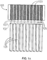
FIG. 1A schematically illustrates a diode laser fiber array for use with the present technology; -
FIG. 1B schematically illustrates another diode laser fiber array for use with the present technology; -
FIG. 1C schematically illustrates another diode laser fiber array for use with the present technology; -
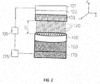
FIG. 2 schematically illustrates a system for simultaneous melting of a powder bed layer by a diode laser fiber array according to an example of the present technology; -
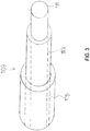
FIG. 3 schematically illustrates a fiber optic construction usable in a diode laser fiber array according to an example of the present technology; -
FIG. 4A schematically illustrates a fiber array usable with the system according to the present technology; and -
FIG. 4B schematically illustrates another fiber array usable with the system according to the present technology. - Referring to
FIG. 1A , a diode laser array 101 (e.g., a diode laser bar or stack) includes a plurality of diode lasers, or emitters, 103, each emitting a beam ofradiation 105. A plurality ofcylindrical lenses 107 are positioned between thediode lasers 103 and a plurality ofoptical fibers 109 to couple eachdiode laser 103 to anoptical fiber 109. Theoptical fibers 109 may be provided in abundle 102 between the diode laser array and the free ends of the optical fibers, as shown for example inFIGS. 1A-1C . However, it should be appreciated that diode fiber laser arrays that do not use coupling optics may be used with the present technology, as discussed below. - Referring to
FIG. 1B , the diodelaser fiber array 101 may includelenses 117 at the ends of theoptical fibers 109. Thelenses 117 may be configured to provide collimatedlaser beams 120 from theoptical fibers 109. Referring toFIG. 1C , the diodelaser fiber array 101 may not include optics (e.g. a lens) between thediode lasers 103 and theoptical fibers 109 and the beams ofradiation 105 may be received by theoptical fibers 109 in proximity to thediode lasers 103. Theoptical fibers 109 may havelenses 117 at their respective ends. Thelenses 117 may be configured to provide a predetermined divergence to thelaser beams 120 emitted from theoptical fibers 109. It should also be appreciated that instead of providing lenses that the ends of theoptical fibers 109 may be shaped to provide collimated ordivergent laser beams 120. - Referring to
FIG. 2 , the diodelaser fiber array 101 directslaser beams 120 from theoptical fibers 109 into apowder bed 130 to simultaneously melt all of the desired powder in a layer. To generate a desired pattern, for example of a repair or a component to be fabricated, the requireddiode lasers 103 are turned on to affect the desired simultaneous melting from eachfiber 109. The melting process time for the desired pattern may be less than a second, which is at least two orders of magnitude faster than current scanning processes. - The
powder bed 130 may be provided on acomponent 150, for example an airfoil of a gas turbine engine of an aircraft, which is supported on asupport 170 to provide a repair to the component. Although the present technology may be applicable to the repair function on components, it should be appreciated that the present technology is applicable for the additive manufacturing build of new make components. The powder bed may be provided on thesupport 170 and the diodelaser fiber array 101 used to build or fabricate the component layer by layer. - The
support 170 may be moved by an actuator or anactuator system 175 that is configured to move thesupport 170 in the Z direction (i.e. normal to the powder bed 130) as shown inFIG. 2 . The actuator oractuator system 175 may also be configured to move thesupport 170 in the XY plane as shown inFIG. 2 , although thesupport 170 is not moved in the XY plane during simultaneous melting of the powder bed from eachfiber 109. The actuator oractuator system 175 may be controlled bycontroller 135 that is configured to control the actuator oractuator system 175 and the diodelaser fiber array 101. The actuator oractuator system 175 may include, for example, a linear motor(s) and/or hydraulic and/or pneumatic piston(s) and/or a screw drive mechanism(s) and/or a conveyor. As the diodelaser fiber array 101 is capable of simultaneously melting all of the required powder in the layer for a pattern, there is no need to move either thearray 101 or thepowder bed 130 during melting, for example as is done with current systems in which a laser beam or electron beam is used to scan a layer of powder. - The distance D between the array of optical fibers 109 (i.e. the ends of the optical fibers 109) and the
powder bed 130 may be controlled by moving thesupport 170 in the Z direction. The distance D may depend on the type oflaser beams 120 emitted by the optical fibers 109 (e.g. whether thelaser beams 120 are collimated or divergent, and the amount of divergence), the average output power of eachdiode laser 103, the pulse energy of eachdiode laser 103, the pulse width of eachdiode laser 103, and or the beam distribution (e.g. Gaussian, top hat, etc.). The ends of theoptical fibers 109 may be located at, for example, about 5 mm to about 150 mm, for example about 20 mm to about 80 mm above thepowder bed 130 so that any region of a layer of thepowder bed 130 can be melted at the same time by turning the requireddiode lasers 103 on at the same time. - The
controller 135 controls the turning on and turning off of eachdiode laser 103. The controller may also control the rate at which the power of eachdiode laser 103 is reduced when turned off. Thecontroller 135 may turn eachdiode laser 103 on and off within a time frame of, for example, about 5 to 15 milliseconds, or longer if needed. For a given layer ofpowder 130, for example above an airfoil to be repaired, the desiredlaser diodes 103 are activated to melt the powder in the desired shape per a CAD design, which may be input and/or stored in thecontroller 135. This process may be repeated as many times as necessary to build up the required repair region. In the case of the system being used to fabricate a component, e.g. an airfoil, the process is repeated as many times as necessary to build the component. Thecontroller 135 controls the actuator oractuator 175 to move thesupport 170 downwardly as layers of powder are added and subsequently processed by the diode laser fiber array. Each layer formed may be, for example, about 1 µm to about 1 mm thick. In the case of repair of an airfoil, each layer may be formed, for example, about 100 µm thick. - The
controller 135 may be a computer processor or other logic-based device, software components (e.g., software applications), and/or a combination of hardware components and software components (e.g., a computer processor or other logic-based device and associated software application, a computer processor, or other logic-based device having hard-wired control instructions, or the like). - The diode
laser fiber array 101 may be controlled by thecontroller 135 to control the heat of powder near or adjacent to the melted region to control the cooling rate of the melted region. Thecontroller 135 may also control the diodelaser fiber array 101 to preheat thepowder bed 130 and/or thecomponent 150. The pre-heating power densities of thediode lasers 103 may be from about 100-100,000 watts/cm2. By pre-heating thepowder bed 130 and/or thecomponent 150 and/or heating the region near or adjacent to the melt region, the thermal gradient may be controlled to be substantially only in the direction normal to the powder bed (i.e. in the Z direction inFIG. 2 ). This may help with materials that are crack sensitive to fast solidification cooling rates. Desirable grain growth that's normal to the layer surface may be achievable with planar cooling of a powder bed layer. This allows formation of a directionally solidified (DS) type grain structure and a single crystal structure with the build repair of an airfoil type structure. It should also be appreciated that thediode lasers 103 may be controlled to superheat thepowder bed 130 to control the viscosity of the melted region. Controlling the viscosity of the melted region allows control over, for example, evaporation of the powder, the grain structure of the solidified layer, and/or the surface finish of the repair or component. - The material in the
powder bed 130 may be metal powder, for example, CoCrMo powder. It should be appreciated that other materials, for example plastic, ceramic, or glass, may be used for the powder bed. Depending on the material in the powder bed, the power of eachdiode laser 103 may be from about 10 to about 60 watts. The power of thediode lasers 103 that are used may be related to the diameter of theoptical fibers 109 used. The power density of thediode lasers 103 may be up to about 1,000,000 watts/cm2 for melting the powder within a layer from each fiber. - The fiber centering position in the fiber array (e.g. as shown in
FIGS. 4A and 4B ) is set by the diameter of a buffer, or coating 115 of theoptical fiber 109. Referring toFIG. 3 , theoptical fiber 109 comprises acore 111, formed of for example silica, andcladding 113, formed for example of silica, around thecore 111. In order to create a numerical aperture and provide total internal reflection within thefiber 109, the refractory index of the silica core may be larger than the refractory index of the silica cladding. For example, the silica core may have a refractive index of about 1.45 and the silica cladding may have a refractive index of about 1.43. Thecladding 113 may have a thickness of about 10 µm. - The buffer, or coating, 115 surrounds the
cladding 113 and may be formed of, for example, acrylate. To reduce the center spacing between theoptical fibers 109, the buffer (acrylate coating) 115 may be replaced by a thinner acrylate coating to reduce the overall fiber diameter. The thickness of the buffer, orcoating 115 may be about 62 µm. The total diameter of thefiber 109 may be about 200 µm to about 250 µm. - The diameter of the
fiber core 111 may be about 105 µm. It should be appreciated that fiber core diameters of about 60 µm may be used. In addition, it should be appreciated thatoptical fibers 109 of various cross sections, may be used. For example, square fibers may be used to increase fiber packing. The melt pool size produced by the laser beam(s) 120 from eachoptical fiber 109 corresponds to the effective laser spot size produced by the laser beam(s) 120. In the case of collimatedlaser beams 120, the melt pool size corresponds generally to the diameter of thefiber core 111. However, thelaser beams 120 from thefibers 109 may be controlled to produce a melt pool size that is, for example, two to four times as large as the diameter of thefiber core 111. Thelaser beams 120 may be controlled to have a divergence to provide a melt pool size larger than the diameter of thefiber core 111. In the case ofdivergent laser beams 120, the distance D from the ends of thefibers 109 of thearray 101 to thepowder bed 130 will also influence the melt pool size of each fiber. The pulse width of the laser beams and the laser beam profiles may also be controlled to adjust the melt pool size provided by each fiber. - Referring to
FIGS. 4A and 4B , the array offibers 109 may be linear as shown inFIG. 4A or closed packed arrangement as shown inFIG. 4B . Other arrays, for example hexagonal, may be used. It should also be appreciated that the array may be in a shape corresponding to the shape of a component to be fabricated. The spacing between thefibers 109 may be equal to the diameter of the buffer, or coating, 115. - The diode laser fiber array of the present technology may be used to process a powder bed layer by exposing the layer with simultaneous laser energy from required diode laser beam sources. The present technology also allows melting the complete pattern in the layer in one time frame that could be less than a second and, when required, control the heat of the powder near and/or adjacent to the melted region to control the cooling rate of the melted region. The diode laser fiber array allows permits grain structure control. The commercial advantages for diode laser fiber array systems include fewer required systems to produce the same amount of parts as current systems and tailoring power bed systems to the size of the parts of interest. The technology disclosed herein may also be used to perform sintering, for example direct metal laser sintering.
- It is to be understood that not necessarily all such objects or advantages described above may be achieved in accordance with any particular example. Thus, for example, those skilled in the art will recognize that the systems and techniques described herein may be embodied or carried out in a manner that achieves or optimizes one advantage or group of advantages as taught herein without necessarily achieving other objects or advantages as may be taught or suggested herein.
- While only certain features of the present technology have been illustrated and described herein, many modifications and changes will occur to those skilled in the art. It is, therefore, to be understood that the appended claims are intended to cover all such modifications and changes.
- Various aspects and embodiments of the invention are defined by the following clauses:
- 1. A method of forming a build in a powder bed, comprising:
- emitting a plurality of laser beams from selected fibers of a diode laser fiber array onto the powder bed, the selected fibers of the array corresponding to a pattern of a layer of the build; and
- simultaneously melting powder in the powder bed corresponding to the pattern of the layer of the build.
- 2. A method according to clause 1, further comprising:
controlling at least one of a duration of each laser beam, a pulse energy of each diode laser, a pulse width of each diode laser, an average output power of each diode laser, an energy distribution of each laser beam, power density of each laser beam, a rate of reduction of the power of each laser beam, and/or a distance of ends of the fibers from the powder bed. - 3. A method according to clause 2, wherein the average output power of each diode laser is up to about 60 W.
- 4. A method according to clause 2, wherein the average output power of each diode laser is between about 2 W to about 60 W.
- 5. A method according to clause 2, wherein the power density of each laser beam is about 1,000,000 W/cm2.
- 6. A method according to clause 2, wherein the distance of ends of the fibers from the powder bed is between about 5 mm to about 150 mm.
- 7. A method according to clause 2, wherein the energy distribution of each laser beam is Gaussian or a top hat.
- 8. A method according to clause 1, wherein the powder is metal, ceramic, glass or plastic.
- 9. A method according to clause 1, further comprising:
- emitting laser beams from fibers at least adjacent to the pattern of the layer; and
- heating the powder adjacent to the powder of the layer of the build to control a cooling rate of the melted powder.
- 10. A method according to clause 9, wherein heating the powder adjacent to the powder of the layer comprises heating the powder at least one of prior to and/or during and/or after simultaneous melting of the powder of the pattern of the layer.
- 11. A method according to clause 9, wherein a power density of the laser beams heating the powder adjacent the pattern is in a range of from about 100 W/cm2 to about 100,000 W/cm2.
- 12. A method according to clause 1, wherein a thickness of each layer is between about 1 µm to about 1 mm.
- 13. A method according to clause 12, wherein a thickness of each layer is about 100 µm.
- 14. A method according to clause 1, wherein the build is a repair of a component.
- 15. A method according to clause 14, wherein the component is a turbine component.
- 16. A method according to clause 15, wherein the turbine component is an airfoil.
- 17. A method according to clause 1, wherein the build is a component of a turbine.
- 18. A method according to clause 17, wherein the component is an airfoil.
- 19. A method according to clause 1, further comprising:
repeating the emitting and simultaneous melting to form a plurality of layers of the build. - 20. A method according to clause 1, further comprising:
allowing the melted powder to cool and solidify. - 21. A method according to clause 1, further comprising:
- moving the selected fibers and the powder bed relative to each other; and
- simultaneously controlling the diode lasers of the selected fibers during relative movement.
- 22. An apparatus for forming a build in a powder bed, comprising:
- a diode laser fiber array comprising a plurality of diode lasers and a plurality of optical fibers corresponding to the plurality of diode lasers, each optical fiber configured to receive a laser beam from a respective diode laser and configured to emit the laser beam;
- a support configured to support a powder bed or a component configured to support the powder bed at a distance from ends of the optical fibers; and
- a controller configured to control the diode laser fiber array to emit a plurality of laser beams from selected fibers of the diode laser fiber array onto the powder bed, the selected fibers of the array corresponding to a pattern of a layer of the build and simultaneously melt the powder in the powder bed corresponding to the pattern of the layer of the build.
- 23. An apparatus according to clause 22, wherein the controller is further configured to control at least one of a duration of each laser beam, a pulse energy of each diode laser, a pulse width of each diode laser, an average output power of each diode laser, an energy distribution of each laser beam, power density of each laser beam, a rate of reduction of the power of each laser beam, and/or a distance of ends of the fibers from the powder bed.
- 24. An apparatus according to clause 22, wherein the controller is further to control the diode laser fiber array to emit laser beams from fibers adjacent to the pattern of the layer and heat the powder adjacent to the powder of the layer of the build to control a cooling rate of the melted powder.
- 25. An apparatus according to clause 24, wherein the controller is configured to control the diode laser fiber array to heat the powder adjacent to the powder of the layer at least one of prior to and/or during simultaneous melting of the powder of the pattern of the layer.
- 26. An apparatus according to clause 22, wherein the optical fibers are provided in a plurality of linear arrays.
- 27. An apparatus according to clause 26, wherein the plurality of linear arrays are arranged in closed packed configuration.
- 28. An apparatus according to clause 22, wherein each optical fiber comprises a core, a cladding surrounding the core, and a buffer surrounding the cladding.
- 29. An apparatus according to clause 28, wherein the core and the cladding are formed of silica, and a refractive index of the core is larger than a refractive index of the cladding.
- 30. An apparatus according to clause 29, wherein a diameter of the core is from about 60 µm to about 105 µm.
- 31. An apparatus according to clause 30, wherein a thickness of the cladding is about 10 µm
- 32. An apparatus according to clause 31, wherein the buffer is formed of acrylate or polyimide.
- 33. An apparatus according to clause 32, wherein a thickness of the buffer is about 62 µm.
- 34. An apparatus according to clause 28, wherein a diameter of each optical fiber is about 250 µm.
- 35. An apparatus according to clause 22, wherein the fibers have circular cross sections.
- 36. An apparatus according to clause 22, further comprising:
at least one lens, the at least one lens being configured to collimate the laser beams. - 37. An apparatus according to clause 22, further comprising:
at least one lens, the at least one lens being configured to provide a predetermined divergence to each of the laser beams. - 38. An apparatus according to clause 22, further comprising:
an actuator configured to move the support, wherein the controller is configured to control the actuator to adjust the distance between the powder bed and the ends of the optical fibers.
Claims (15)
- An apparatus for forming a build in a powder bed, the apparatus comprising:a diode laser fiber array comprising a plurality of diode lasers and a plurality of optical fibers corresponding to the plurality of diode lasers, wherein respective ones of the plurality of optical fibers are configured to receive a laser beam from a corresponding one of the plurality of diode lasers and to emit the laser beam;a support configured to support a powder bed or a component configured to support the powder bed at a distance from ends of the plurality of optical fibers; anda controller configured to control the diode laser fiber array to emit a plurality of laser beams onto the powder bed from selected ones of the plurality of optical fibers of the diode laser fiber array, the selected ones of the plurality of optical fibers corresponding to a pattern of a layer of the build such that the plurality of laser beams from the selected ones of the plurality of optical fibers simultaneously melt a portion of the powder bed corresponding to the pattern of the layer of the build.
- An apparatus according to claim 1, wherein the controller is configured to control at least one of:an emission duration of the respective laser beams emitted from the plurality of diode lasers corresponding to the selected ones of the plurality of optical fibers of the diode laser fiber array;a pulse energy of the respective laser beams emitted from the plurality of diode lasers corresponding to the selected ones of the plurality of optical fibers of the diode laser fiber array;a pulse width of the respective laser beams emitted from the plurality of diode lasers corresponding to the selected ones of the plurality of optical fibers of the diode laser fiber array;an average output power of the respective laser beams emitted from the plurality of diode lasers corresponding to the selected ones of the plurality of optical fibers of the diode laser fiber array;an energy distribution of the respective laser beams emitted from the plurality of diode lasers corresponding to the selected ones of the plurality of optical fibers of the diode laser fiber array;a power of the respective laser beams emitted from the plurality of diode lasers corresponding to the selected ones of the plurality of optical fibers of the diode laser fiber array;a rate of reduction of the power of the respective laser beams emitted from the plurality of diode lasers corresponding to the selected ones of the plurality of optical fibers of the diode laser fiber array; and/ora distance of from the powder bed of the plurality of diode lasers corresponding to the selected ones of the plurality of optical fibers of the diode laser fiber array.
- An apparatus according to claim 1 or 2, wherein the controller is configured to control the diode laser fiber array to emit laser beams from additional selected ones of the plurality optical fibers of the diode laser array, the additional selected ones of the plurality of optical fibers being selected so as to emit a plurality of laser beams onto the powder bed adjacent to the pattern of the layer of the build, thereby heating a portion of the powder bed adjacent to the pattern of the layer of the build, and/or thereby controlling a cooling rate of the melted powder and/or at least a portion of the powder bed.
- An apparatus according to any one of claims 1 to 3, wherein the controller is configured to control the diode laser fiber array so as to heat the portion of the powder bed adjacent the pattern of the layer of the build at least prior to and/or during simultaneous melting of the portion of the powder bed corresponding to the pattern of the layer of the build.
- An apparatus according to any one of claims 1 to 4, wherein the optical fibers are provided in a plurality of linear arrays, especially a plurality of linear arrays arranged in a closed packed configuration.
- An apparatus according to any one of claims 1 to 5, wherein respective ones of the plurality of optical fiber comprise a core, a cladding surrounding the core, and a buffer surrounding the cladding.
- An apparatus according to claim 6, wherein the core and the cladding are formed of a material comprising silica, and wherein a refractive index of the core is larger than a refractive index of the cladding.
- An apparatus according to claim 7, wherein a diameter of the core is from 60 µm to 105 µm.
- An apparatus according to claim 8, wherein the buffer is formed of a material comprising an acrylate and/or a polyimide.
- An apparatus according to any one of claims 1 to 9, comprising:at least one lens configured to collimate the plurality of laser beams; and/orat least one lens configured to provide a predetermined divergence to respective ones of the plurality of laser beams.
- An apparatus according to any one of claims 1 to 10, comprising:
an actuator configured to move the support, wherein the controller is configured to control the actuator to adjust the distance from the powder bed to the ends of the optical fibers, the distance in particular being from about 5 mm to about 150 mm. - An apparatus according to any one of claims 1 to 11, wherein the average output power of respective ones of the plurality of diode lasers is up to about 60 W, especially between about 2 W to about 60 W.
- An apparatus according to any one of claims 1 to 12, wherein, the power density of a respective one of the plurality of laser beams is about 1,000,000 W/cm2; and/or wherein the energy distribution of a respective one of the plurality of laser beams is a Gaussian distribution or a top hat distribution; and/or wherein a respective one of the plurality of diode lasers is configured to emit a laser beam for 5 to 15 milliseconds.
- An apparatus according to any one of claims 1 to 13, wherein the controller is configured to control the diode laser fiber array to:turn on selected diode lasers of a diode laser fiber array, the selected lasers of the diode laser fiber array corresponding to a desired pattern of a layer of the build; andturn off the selected diode lasers.
- A method of forming a build in a powder bed, wherein the method is performed using an apparatus according to any one of claims 1-14.
Applications Claiming Priority (3)
| Application Number | Priority Date | Filing Date | Title |
|---|---|---|---|
| US14/106,970 US10328685B2 (en) | 2013-12-16 | 2013-12-16 | Diode laser fiber array for powder bed fabrication or repair |
| PCT/US2014/068979 WO2015134075A2 (en) | 2013-12-16 | 2014-12-08 | Diode laser fiber array for powder bed fabrication or repair |
| EP14882786.8A EP3083111B1 (en) | 2013-12-16 | 2014-12-08 | Diode laser fiber array for powder bed fabrication or repair |
Related Parent Applications (2)
| Application Number | Title | Priority Date | Filing Date |
|---|---|---|---|
| EP14882786.8A Division EP3083111B1 (en) | 2013-12-16 | 2014-12-08 | Diode laser fiber array for powder bed fabrication or repair |
| EP14882786.8A Division-Into EP3083111B1 (en) | 2013-12-16 | 2014-12-08 | Diode laser fiber array for powder bed fabrication or repair |
Publications (2)
| Publication Number | Publication Date |
|---|---|
| EP3593926A1 true EP3593926A1 (en) | 2020-01-15 |
| EP3593926B1 EP3593926B1 (en) | 2022-11-09 |
Family
ID=53367280
Family Applications (2)
| Application Number | Title | Priority Date | Filing Date |
|---|---|---|---|
| EP14882786.8A Active EP3083111B1 (en) | 2013-12-16 | 2014-12-08 | Diode laser fiber array for powder bed fabrication or repair |
| EP19195164.9A Active EP3593926B1 (en) | 2013-12-16 | 2014-12-08 | Diode laser fiber array for powder bed fabrication or repair |
Family Applications Before (1)
| Application Number | Title | Priority Date | Filing Date |
|---|---|---|---|
| EP14882786.8A Active EP3083111B1 (en) | 2013-12-16 | 2014-12-08 | Diode laser fiber array for powder bed fabrication or repair |
Country Status (7)
| Country | Link |
|---|---|
| US (4) | US10328685B2 (en) |
| EP (2) | EP3083111B1 (en) |
| JP (1) | JP6225263B2 (en) |
| CN (2) | CN112600062B (en) |
| BR (1) | BR112016012234B1 (en) |
| CA (1) | CA2932620C (en) |
| WO (1) | WO2015134075A2 (en) |
Families Citing this family (117)
| Publication number | Priority date | Publication date | Assignee | Title |
|---|---|---|---|---|
| CN105144346B (en) | 2013-02-21 | 2017-12-15 | 恩耐公司 | The laser scribing of sandwich construction |
| US10464172B2 (en) | 2013-02-21 | 2019-11-05 | Nlight, Inc. | Patterning conductive films using variable focal plane to control feature size |
| US9842665B2 (en) | 2013-02-21 | 2017-12-12 | Nlight, Inc. | Optimization of high resolution digitally encoded laser scanners for fine feature marking |
| US11612957B2 (en) * | 2016-04-29 | 2023-03-28 | Nuburu, Inc. | Methods and systems for welding copper and other metals using blue lasers |
| US10971896B2 (en) | 2013-04-29 | 2021-04-06 | Nuburu, Inc. | Applications, methods and systems for a laser deliver addressable array |
| US10940562B2 (en) | 2017-01-31 | 2021-03-09 | Nuburu, Inc. | Methods and systems for welding copper using blue laser |
| US10562132B2 (en) | 2013-04-29 | 2020-02-18 | Nuburu, Inc. | Applications, methods and systems for materials processing with visible raman laser |
| US10532556B2 (en) | 2013-12-16 | 2020-01-14 | General Electric Company | Control of solidification in laser powder bed fusion additive manufacturing using a diode laser fiber array |
| US20170021456A1 (en) * | 2014-04-10 | 2017-01-26 | Ge Avio S.R.L. | Process for forming a component by means of additive manufacturing, and powder dispensing device for carrying out such a process |
| US10069271B2 (en) | 2014-06-02 | 2018-09-04 | Nlight, Inc. | Scalable high power fiber laser |
| US10618131B2 (en) | 2014-06-05 | 2020-04-14 | Nlight, Inc. | Laser patterning skew correction |
| US10310201B2 (en) | 2014-08-01 | 2019-06-04 | Nlight, Inc. | Back-reflection protection and monitoring in fiber and fiber-delivered lasers |
| US11646549B2 (en) | 2014-08-27 | 2023-05-09 | Nuburu, Inc. | Multi kW class blue laser system |
| US9837783B2 (en) | 2015-01-26 | 2017-12-05 | Nlight, Inc. | High-power, single-mode fiber sources |
| US10589466B2 (en) * | 2015-02-28 | 2020-03-17 | Xerox Corporation | Systems and methods for implementing multi-layer addressable curing of ultraviolet (UV) light curable inks for three dimensional (3D) printed parts and components |
| US10050404B2 (en) | 2015-03-26 | 2018-08-14 | Nlight, Inc. | Fiber source with cascaded gain stages and/or multimode delivery fiber with low splice loss |
| CN107635749A (en) * | 2015-06-10 | 2018-01-26 | Ipg光子公司 | Multiple beam increasing material manufacturing |
| DE102015211494A1 (en) * | 2015-06-22 | 2016-12-22 | Eos Gmbh Electro Optical Systems | Device and method for producing a three-dimensional object |
| WO2017008022A1 (en) | 2015-07-08 | 2017-01-12 | Nlight, Inc. | Fiber with depressed central index for increased beam parameter product |
| US9884393B2 (en) * | 2015-10-20 | 2018-02-06 | General Electric Company | Repair methods utilizing additively manufacturing for rotor blades and components |
| JP6801173B2 (en) * | 2015-10-29 | 2020-12-16 | セイコーエプソン株式会社 | Manufacturing method of three-dimensional structure, its manufacturing equipment and its control program |
| WO2017071760A1 (en) * | 2015-10-29 | 2017-05-04 | Hewlett-Packard Development Company, L P | Additive manufacturing method using an energy source and varying build material spacings and apparatus |
| US11691341B2 (en) | 2015-10-30 | 2023-07-04 | Seurat Technologies, Inc. | Part manipulation using printed manipulation points |
| US10717263B2 (en) | 2015-11-13 | 2020-07-21 | Paxis Llc | Additive manufacturing apparatus, system, and method |
| PL3374163T3 (en) * | 2015-11-13 | 2023-04-24 | Paxis Llc | Additive manufacturing apparatus, system, and method |
| DE102015119745A1 (en) * | 2015-11-16 | 2017-05-18 | Cl Schutzrechtsverwaltungs Gmbh | Device for the generative production of a three-dimensional object |
| US11179807B2 (en) | 2015-11-23 | 2021-11-23 | Nlight, Inc. | Fine-scale temporal control for laser material processing |
| US10434600B2 (en) | 2015-11-23 | 2019-10-08 | Nlight, Inc. | Fine-scale temporal control for laser material processing |
| US10074960B2 (en) | 2015-11-23 | 2018-09-11 | Nlight, Inc. | Predictive modification of laser diode drive current waveform in order to optimize optical output waveform in high power laser systems |
| US20170157857A1 (en) * | 2015-12-07 | 2017-06-08 | United Technologies Corporation | Adjusting process parameters to reduce conglomerated powder |
| US10471543B2 (en) | 2015-12-15 | 2019-11-12 | Lawrence Livermore National Security, Llc | Laser-assisted additive manufacturing |
| US10583532B2 (en) * | 2015-12-28 | 2020-03-10 | General Electric Company | Metal additive manufacturing using gas mixture including oxygen |
| US10295820B2 (en) | 2016-01-19 | 2019-05-21 | Nlight, Inc. | Method of processing calibration data in 3D laser scanner systems |
| CN108495741B (en) | 2016-01-20 | 2020-08-04 | 惠普发展公司,有限责任合伙企业 | printing equipment |
| US10744562B2 (en) | 2016-01-25 | 2020-08-18 | General Electric Company | Additive manufacturing employing a plurality of electron beam sources |
| WO2017132664A1 (en) | 2016-01-28 | 2017-08-03 | Seurat Technologies, Inc. | Additive manufacturing, spatial heat treating system and method |
| EP3995277A1 (en) | 2016-01-29 | 2022-05-11 | Seurat Technologies, Inc. | System for additive manufacturing |
| JP6553102B2 (en) * | 2016-02-03 | 2019-07-31 | ゼネラル・エレクトリック・カンパニイ | Solidification control method in laser powder bed fusion bond addition manufacturing using diode laser fiber array |
| US11980970B2 (en) | 2016-04-29 | 2024-05-14 | Nuburu, Inc. | Visible laser additive manufacturing |
| US12172377B2 (en) | 2016-04-29 | 2024-12-24 | Nuburu, Inc. | Blue laser metal additive manufacturing system |
| US20220072659A1 (en) * | 2016-04-29 | 2022-03-10 | Nuburu, Inc. | Methods and Systems for Reducing Hazardous Byproduct from Welding Metals Using Lasers |
| CN105834427B (en) * | 2016-05-27 | 2018-01-05 | 西安交通大学 | The device and method of brilliant part is oriented using the 3D printing of multiple laser aids in temperature control |
| US10069996B2 (en) * | 2016-09-15 | 2018-09-04 | Xerox Corporation | System and method for utilizing digital micromirror devices to split and recombine a signal image to enable heat dissipation |
| US10730785B2 (en) | 2016-09-29 | 2020-08-04 | Nlight, Inc. | Optical fiber bending mechanisms |
| US10732439B2 (en) | 2016-09-29 | 2020-08-04 | Nlight, Inc. | Fiber-coupled device for varying beam characteristics |
| DE102016218887A1 (en) * | 2016-09-29 | 2018-03-29 | SLM Solutions Group AG | Producing three-dimensional workpieces by means of a plurality of irradiation units |
| US10295845B2 (en) | 2016-09-29 | 2019-05-21 | Nlight, Inc. | Adjustable beam characteristics |
| US10471695B2 (en) * | 2016-10-26 | 2019-11-12 | General Electric Company | Methods and thermal structures for additive manufacturing |
| US10589508B2 (en) * | 2016-12-15 | 2020-03-17 | General Electric Company | Additive manufacturing systems and methods |
| GB201701355D0 (en) | 2017-01-27 | 2017-03-15 | Renishaw Plc | Direct laser writing and chemical etching |
| US11117193B2 (en) * | 2017-02-01 | 2021-09-14 | Hrl Laboratories, Llc | Additive manufacturing with nanofunctionalized precursors |
| US11548094B2 (en) * | 2017-02-15 | 2023-01-10 | General Electric Company | System and methods for fabricating a component with laser array |
| US11484970B2 (en) * | 2017-02-21 | 2022-11-01 | General Electric Company | Additive manufacturing system and method of forming an object in a powder bed |
| DE102017104097A1 (en) * | 2017-02-28 | 2018-08-30 | Pac Tech-Packaging Technologies Gmbh | Method and laser arrangement for melting a solder material deposit by means of laser energy |
| DE102017105057A1 (en) | 2017-03-09 | 2018-09-13 | Cl Schutzrechtsverwaltungs Gmbh | Exposure device for a device for the additive production of three-dimensional objects |
| US10906132B2 (en) | 2017-03-31 | 2021-02-02 | General Electric Company | Scan strategies for efficient utilization of laser arrays in direct metal laser melting (DMLM) |
| EP3607389B1 (en) | 2017-04-04 | 2023-06-07 | Nlight, Inc. | Optical fiducial generation for galvanometric scanner calibration |
| EP4220252A3 (en) | 2017-04-21 | 2023-08-09 | Nuburu, Inc. | Multi-clad optical fiber |
| US20180311757A1 (en) * | 2017-04-28 | 2018-11-01 | Divergent Technologies, Inc. | Additive manufacturing control systems |
| US20180311760A1 (en) * | 2017-04-28 | 2018-11-01 | Divergent Technologies, Inc. | Powder-bed fusion beam scanning |
| WO2018209226A1 (en) | 2017-05-11 | 2018-11-15 | Seurat Technologies, Inc. | Solid state routing of patterned light for additive manufacturing optimization |
| JP7136811B2 (en) | 2017-05-11 | 2022-09-13 | シューラット テクノロジーズ,インク. | Switchyard Beam Routing of Patterned Light for Additive Manufacturing |
| WO2018231884A1 (en) | 2017-06-13 | 2018-12-20 | Nuburu, Inc. | Very dense wavelength beam combined laser system |
| US11084132B2 (en) * | 2017-10-26 | 2021-08-10 | General Electric Company | Diode laser fiber array for contour of powder bed fabrication or repair |
| US10845506B2 (en) | 2017-11-16 | 2020-11-24 | The Boeing Company | Topological insulator protected optical elements |
| US10186351B1 (en) | 2017-11-16 | 2019-01-22 | The Boeing Company | Topological insulator tubes applied to signal transmission systems |
| US10987825B2 (en) | 2017-11-16 | 2021-04-27 | The Boeing Company | Topological insulator nanotube device and methods of employing the nanotube device |
| US10405465B2 (en) | 2017-11-16 | 2019-09-03 | The Boeing Company | Topological insulator thermal management systems |
| US10887996B2 (en) | 2017-11-16 | 2021-01-05 | The Boeing Company | Electronic components coated with a topological insulator |
| US10814600B2 (en) | 2017-11-16 | 2020-10-27 | The Boeing Company | Methods of and systems for forming coatings that comprise non-carbon-based topological insulators |
| US10444883B2 (en) | 2017-11-16 | 2019-10-15 | The Boeing Company | Touch screen display including topological insulators |
| US10821551B2 (en) | 2018-01-26 | 2020-11-03 | General Electronic Company | Systems and methods for dynamic shaping of laser beam profiles in additive manufacturing |
| US10814429B2 (en) | 2018-01-26 | 2020-10-27 | General Electric Company | Systems and methods for dynamic shaping of laser beam profiles for control of micro-structures in additively manufactured metals |
| US11772163B2 (en) * | 2018-02-09 | 2023-10-03 | Hewlett-Packard Development Company, L.P. | Three-dimensional printing systems |
| US10875094B2 (en) * | 2018-03-29 | 2020-12-29 | Vulcanforms Inc. | Additive manufacturing systems and methods |
| CA3096390C (en) | 2018-04-06 | 2023-10-17 | Paxis Llc | Additive manufacturing apparatus, system, and method |
| CN108526653B (en) * | 2018-05-03 | 2020-04-21 | 温州大学激光与光电智能制造研究院 | A metal three-dimensional printing method based on parallel pulsed arc melting |
| GB201807830D0 (en) | 2018-05-15 | 2018-06-27 | Renishaw Plc | Laser beam scanner |
| US20210205892A1 (en) * | 2018-06-08 | 2021-07-08 | Hewlett-Packard Development Company, L.P. | Printing devices |
| US11426818B2 (en) | 2018-08-10 | 2022-08-30 | The Research Foundation for the State University | Additive manufacturing processes and additively manufactured products |
| WO2020107030A1 (en) | 2018-11-23 | 2020-05-28 | Nuburu, Inc | Multi-wavelength visible laser source |
| US11465353B2 (en) * | 2018-11-30 | 2022-10-11 | Photofusion Technologies Limited | High mobility 3D laser printing system |
| CN113195127A (en) | 2018-12-14 | 2021-07-30 | 速尔特技术有限公司 | Additive manufacturing system for creating objects from powder using high-throughput laser for two-dimensional printing |
| WO2020132215A1 (en) | 2018-12-19 | 2020-06-25 | Seurat Technologies, Inc. | Additive manufacturing system using a pulse modulated laser for two-dimensional printing |
| WO2020131400A1 (en) | 2018-12-21 | 2020-06-25 | Corning Incorporated | Strengthened 3d printed surface features and methods of making the same |
| US11426799B2 (en) | 2019-01-30 | 2022-08-30 | General Electric Company | Powder seal assembly for decreasing powder usage in a powder bed additive manufacturing process |
| US11344979B2 (en) | 2019-01-30 | 2022-05-31 | General Electric Company | Build plate clamping-assembly and additive manufacturing systems and methods of additively printing on workpieces |
| US11465245B2 (en) | 2019-01-30 | 2022-10-11 | General Electric Company | Tooling assembly for magnetically aligning components in an additive manufacturing machine |
| US11198182B2 (en) | 2019-01-30 | 2021-12-14 | General Electric Company | Additive manufacturing systems and methods of additively printing on workpieces |
| US20200238386A1 (en) | 2019-01-30 | 2020-07-30 | General Electric Company | Tooling Assembly for Decreasing Powder Usage in a Powder Bed Additive Manufacturing Process |
| US11173574B2 (en) | 2019-01-30 | 2021-11-16 | General Electric Company | Workpiece-assembly and additive manufacturing systems and methods of additively printing on workpieces |
| US11144034B2 (en) | 2019-01-30 | 2021-10-12 | General Electric Company | Additive manufacturing systems and methods of generating CAD models for additively printing on workpieces |
| US11407035B2 (en) | 2019-01-30 | 2022-08-09 | General Electric Company | Powder seal assembly for decreasing powder usage in a powder bed additive manufacturing process |
| US11285538B2 (en) | 2019-01-30 | 2022-03-29 | General Electric Company | Tooling assembly and method for aligning components for a powder bed additive manufacturing repair process |
| US11458681B2 (en) | 2019-01-30 | 2022-10-04 | General Electric Company | Recoating assembly for an additive manufacturing machine |
| US11498132B2 (en) | 2019-01-30 | 2022-11-15 | General Electric Company | Additive manufacturing systems and methods of calibrating for additively printing on workpieces |
| EP3917718A4 (en) | 2019-02-02 | 2022-12-07 | Nuburu, Inc. | HIGH-BRIGHTNESS, HIGH-POWER, HIGH-RELIABILITY BLUE LASER DIODE SYSTEMS AND METHODS OF MAKING THEREOF |
| CN110039048B (en) * | 2019-03-29 | 2021-05-04 | 西北大学 | Linear array high-speed laser 3D metal printer and its printing control method |
| US11298884B2 (en) | 2019-06-07 | 2022-04-12 | General Electric Company | Additive manufacturing systems and methods of pretreating and additively printing on workpieces |
| US11230058B2 (en) | 2019-06-07 | 2022-01-25 | The Boeing Company | Additive manufacturing using light source arrays to provide multiple light beams to a build medium via a rotatable reflector |
| DE102019126888A1 (en) * | 2019-10-07 | 2021-04-08 | LIMO GmbH | Laser device for generating laser radiation and 3D printing device with such a laser device |
| CN114631047A (en) | 2019-10-07 | 2022-06-14 | Limo有限责任公司 | Laser device for generating laser radiation and 3D printing apparatus comprising such a laser device |
| CN110757793A (en) * | 2019-11-05 | 2020-02-07 | 北京易加三维科技有限公司 | Scanning system based on dense laser array, additive manufacturing equipment and manufacturing method |
| FR3107846B1 (en) * | 2020-03-03 | 2022-06-17 | Safran Aircraft Engines | METHOD AND ENDOSCOPE FOR CLEANING A TURBOMACHINE BLADE |
| CN111324969B (en) * | 2020-03-06 | 2023-03-24 | 南京理工大学 | Phase field simulation method for temperature gradient regulation and control of layered superalloy microstructure |
| US12358222B2 (en) | 2020-08-14 | 2025-07-15 | Paxis Llc | Additive manufacturing apparatus, system, and method |
| US12162074B2 (en) | 2020-11-25 | 2024-12-10 | Lawrence Livermore National Security, Llc | System and method for large-area pulsed laser melting of metallic powder in a laser powder bed fusion application |
| CN112643056B (en) * | 2020-12-18 | 2022-11-08 | 中国科学院上海光学精密机械研究所 | Surface Scanning Laser Additive Manufacturing Device Based on Double Pulse Light Source Illumination |
| US12377469B2 (en) | 2021-03-02 | 2025-08-05 | General Electric Company | Recoater for additive manufacturing |
| US12042866B2 (en) | 2021-03-16 | 2024-07-23 | General Electric Company | Additive manufacturing apparatus and fluid flow mechanism |
| RU208724U1 (en) * | 2021-05-21 | 2022-01-11 | федеральное государственное автономное образовательное учреждение высшего образования "Санкт-Петербургский политехнический университет Петра Великого" (ФГАОУ ВО "СПбПУ") | Forming device for layered growth with heating system |
| WO2023023390A1 (en) | 2021-08-20 | 2023-02-23 | General Electric Company | Irradiation devices with optical modulators for additively manufacturing three-dimensional objects |
| US12030251B2 (en) | 2021-08-20 | 2024-07-09 | General Electric Company | Irradiation devices with optical modulators for additively manufacturing three-dimensional objects |
| PL440030A1 (en) * | 2021-12-29 | 2023-07-03 | Stefan Dobrowolski | Device for additive manufacturing of three-dimensional objects from metals and their alloys |
| CN115090906B (en) * | 2022-06-10 | 2024-12-20 | 中国人民解放军陆军装甲兵学院 | A real-time temperature control system and control method for additive manufacturing deposition process |
| US12558846B2 (en) | 2023-03-06 | 2026-02-24 | General Electric Company | Irradiation devices with optical modulators for additively manufacturing three-dimensional objects |
| US20240408674A1 (en) * | 2023-06-09 | 2024-12-12 | General Electric Company | Systems and methods for additively manufacturing three-dimensional objects with array of laser diodes |
Citations (3)
| Publication number | Priority date | Publication date | Assignee | Title |
|---|---|---|---|---|
| US20030214571A1 (en) * | 2002-04-10 | 2003-11-20 | Fuji Photo Film Co., Ltd. | Exposure head, exposure apparatus, and application thereof |
| US20130064706A1 (en) * | 2009-12-04 | 2013-03-14 | Slm Solutions Gmbh | Optical irradiation unit for a plant for producing workpieces by irradiation of powder layers with laser radiation |
| US20140263209A1 (en) * | 2013-03-15 | 2014-09-18 | Matterfab Corp. | Apparatus and methods for manufacturing |
Family Cites Families (36)
| Publication number | Priority date | Publication date | Assignee | Title |
|---|---|---|---|---|
| CA2075026A1 (en) | 1991-08-08 | 1993-02-09 | William E. Nelson | Method and apparatus for patterning an imaging member |
| US5393482A (en) | 1993-10-20 | 1995-02-28 | United Technologies Corporation | Method for performing multiple beam laser sintering employing focussed and defocussed laser beams |
| US5914059A (en) | 1995-05-01 | 1999-06-22 | United Technologies Corporation | Method of repairing metallic articles by energy beam deposition with reduced power density |
| US5844663A (en) | 1996-09-13 | 1998-12-01 | Electronic Systems Engineering Co. | Method and apparatus for sequential exposure printing of ultra high resolution digital images using multiple multiple sub-image generation and a programmable moving-matrix light valve |
| JP4145978B2 (en) | 1997-11-11 | 2008-09-03 | ナブテスコ株式会社 | Stereolithography apparatus and method |
| DE19905300A1 (en) | 1999-02-09 | 2000-08-10 | Buck Werke Gmbh & Co I K | Purifying and recovering surfactant-containing water from industrial scale washing processes using two bioreactors containing biodegraders of different activity rate |
| DE19953000C2 (en) * | 1999-11-04 | 2003-04-10 | Horst Exner | Method and device for the rapid production of bodies |
| US6423935B1 (en) | 2000-02-18 | 2002-07-23 | The Regents Of The University Of California | Identification marking by means of laser peening |
| WO2002042023A1 (en) | 2000-11-27 | 2002-05-30 | National University Of Singapore | Method and apparatus for creating a three-dimensional metal part using high-temperature direct laser melting |
| US20020149137A1 (en) | 2001-04-12 | 2002-10-17 | Bor Zeng Jang | Layer manufacturing method and apparatus using full-area curing |
| US6980321B2 (en) | 2001-08-20 | 2005-12-27 | Eastman Kodak Company | Method and apparatus for printing high resolution images using multiple reflective spatial light modulators |
| US6975659B2 (en) * | 2001-09-10 | 2005-12-13 | Fuji Photo Film Co., Ltd. | Laser diode array, laser device, wave-coupling laser source, and exposure device |
| JP2003080604A (en) | 2001-09-10 | 2003-03-19 | Fuji Photo Film Co Ltd | Laminate shaping apparatus |
| US6855482B2 (en) | 2002-04-09 | 2005-02-15 | Day International, Inc. | Liquid transfer articles and method for producing the same using digital imaging photopolymerization |
| US6960035B2 (en) * | 2002-04-10 | 2005-11-01 | Fuji Photo Film Co., Ltd. | Laser apparatus, exposure head, exposure apparatus, and optical fiber connection method |
| KR100629209B1 (en) * | 2002-05-23 | 2006-09-27 | 후지 샤신 필름 가부시기가이샤 | Connection method of laser device, exposure head, exposure device and optical fiber |
| CA2568791A1 (en) * | 2004-06-01 | 2005-12-15 | Trumpf Photonics Inc. | Optimum matching of the output of a two-dimensional laser array stack to an optical fiber |
| CN1268047C (en) | 2004-07-06 | 2006-08-02 | 华北工学院 | Method and apparatus for applying optical fiber array energy source to laser sintering rapid forming |
| US7444046B2 (en) | 2005-10-18 | 2008-10-28 | Nlight Photonics Corporation | Diode laser array coupling optic and system |
| DE102006026967A1 (en) | 2006-06-09 | 2007-12-13 | Rolls-Royce Deutschland Ltd & Co Kg | Method for producing a cutting tool |
| GB2453945A (en) | 2007-10-23 | 2009-04-29 | Rolls Royce Plc | Apparatus for Additive Manufacture Welding |
| US9063289B1 (en) * | 2008-06-30 | 2015-06-23 | Nlight Photonics Corporation | Multimode fiber combiners |
| US20100027569A1 (en) * | 2008-07-29 | 2010-02-04 | John Brekke | Uv diode-laser module with optical fiber delivery |
| CN101893736B (en) * | 2010-06-11 | 2012-06-06 | 哈尔滨工程大学 | Array core fiber-based axial array optical tweezer and photodynamic control method |
| US20120065755A1 (en) | 2010-08-13 | 2012-03-15 | Sensable Technologies, Inc. | Fabrication of non-homogeneous articles via additive manufacturing using three-dimensional voxel-based models |
| US9352419B2 (en) | 2011-01-13 | 2016-05-31 | Siemens Energy, Inc. | Laser re-melt repair of superalloys using flux |
| US9283593B2 (en) | 2011-01-13 | 2016-03-15 | Siemens Energy, Inc. | Selective laser melting / sintering using powdered flux |
| US9902113B2 (en) * | 2011-03-17 | 2018-02-27 | Panasonic Intellectual Property Management Co., Ltd. | Method for manufacturing three-dimensional shaped object and three-dimensional shaped object |
| CN102328081B (en) * | 2011-09-26 | 2013-12-25 | 华中科技大学 | Method for rapidly forming three-dimensional metal parts by high-power lasers |
| JP5895172B2 (en) * | 2012-02-09 | 2016-03-30 | パナソニックIpマネジメント株式会社 | Manufacturing method of three-dimensional shaped object |
| ITMI20120331A1 (en) | 2012-03-02 | 2013-09-03 | Legor Group S P A | SILVER-BASED ALLOY POWDER FOR MANUFACTURING OF 3-DIMENSIONAL METAL OBJECTS |
| JP2015529305A (en) * | 2012-09-24 | 2015-10-05 | シーメンス アクチエンゲゼルシヤフトSiemens Aktiengesellschaft | Wind turbine blade |
| WO2014131444A1 (en) | 2013-02-27 | 2014-09-04 | Slm Solutions Gmbh | Apparatus and method for producing work pieces having a tailored microstructure |
| DE102013011676A1 (en) * | 2013-07-11 | 2015-01-15 | Fraunhofer-Gesellschaft zur Förderung der angewandten Forschung e.V. | Device and method for generative component production |
| EP3096905B1 (en) | 2014-01-20 | 2021-12-22 | Raytheon Technologies Corporation | A method of additive manufacturing utilizing an epitaxy process |
| CN107635749A (en) | 2015-06-10 | 2018-01-26 | Ipg光子公司 | Multiple beam increasing material manufacturing |
-
2013
- 2013-12-16 US US14/106,970 patent/US10328685B2/en active Active
-
2014
- 2014-12-08 JP JP2016537994A patent/JP6225263B2/en active Active
- 2014-12-08 CN CN202011248193.4A patent/CN112600062B/en active Active
- 2014-12-08 EP EP14882786.8A patent/EP3083111B1/en active Active
- 2014-12-08 BR BR112016012234-8A patent/BR112016012234B1/en not_active IP Right Cessation
- 2014-12-08 EP EP19195164.9A patent/EP3593926B1/en active Active
- 2014-12-08 WO PCT/US2014/068979 patent/WO2015134075A2/en not_active Ceased
- 2014-12-08 CN CN201480068727.1A patent/CN105814759B/en active Active
- 2014-12-08 CA CA2932620A patent/CA2932620C/en active Active
-
2019
- 2019-05-22 US US16/419,657 patent/US10569525B2/en active Active
-
2020
- 2020-01-15 US US16/743,325 patent/US11027536B2/en active Active
-
2021
- 2021-05-07 US US17/314,606 patent/US20210268789A1/en active Pending
Patent Citations (3)
| Publication number | Priority date | Publication date | Assignee | Title |
|---|---|---|---|---|
| US20030214571A1 (en) * | 2002-04-10 | 2003-11-20 | Fuji Photo Film Co., Ltd. | Exposure head, exposure apparatus, and application thereof |
| US20130064706A1 (en) * | 2009-12-04 | 2013-03-14 | Slm Solutions Gmbh | Optical irradiation unit for a plant for producing workpieces by irradiation of powder layers with laser radiation |
| US20140263209A1 (en) * | 2013-03-15 | 2014-09-18 | Matterfab Corp. | Apparatus and methods for manufacturing |
Also Published As
| Publication number | Publication date |
|---|---|
| EP3593926B1 (en) | 2022-11-09 |
| WO2015134075A3 (en) | 2016-01-28 |
| JP2017502843A (en) | 2017-01-26 |
| US10569525B2 (en) | 2020-02-25 |
| BR112016012234A2 (en) | 2017-08-08 |
| CN112600062B (en) | 2024-08-09 |
| US20210268789A1 (en) | 2021-09-02 |
| CN105814759A (en) | 2016-07-27 |
| US11027536B2 (en) | 2021-06-08 |
| CA2932620A1 (en) | 2015-09-11 |
| US20200223212A1 (en) | 2020-07-16 |
| BR112016012234B1 (en) | 2020-12-08 |
| US20190283392A1 (en) | 2019-09-19 |
| WO2015134075A2 (en) | 2015-09-11 |
| EP3083111A2 (en) | 2016-10-26 |
| US10328685B2 (en) | 2019-06-25 |
| CA2932620C (en) | 2022-01-18 |
| CN105814759B (en) | 2020-11-17 |
| EP3083111B1 (en) | 2019-10-09 |
| CN112600062A (en) | 2021-04-02 |
| US20150165556A1 (en) | 2015-06-18 |
| JP6225263B2 (en) | 2017-11-01 |
Similar Documents
| Publication | Publication Date | Title |
|---|---|---|
| US11027536B2 (en) | Diode laser fiber array for powder bed fabrication or repair | |
| US11020955B2 (en) | Control of solidification in laser powder bed fusion additive manufacturing using a diode laser fiber array | |
| EP3202514B1 (en) | Control of solidification in laser powder bed fusion additive manufacturing using a diode laser fiber array | |
| US11712765B2 (en) | Diode laser fiber array for contour of powder bed fabrication or repair | |
| EP3345698B1 (en) | Powder bed system and methods for fabricating a component with laser array | |
| CN110267796B (en) | Additive manufacturing system and method | |
| EP3541566B1 (en) | Method of controlling the cooling rate of a melt pool of a powder bed, and direct metal laser melting manufacturing system with in-line laser scanner | |
| CN105562688B (en) | Production of components by selective laser melting | |
| US20190275612A1 (en) | Variable beam geometry laser-based powder bed fusion | |
| CN116157227A (en) | Laser heating for the manufacture or repair of turbine blades |
Legal Events
| Date | Code | Title | Description |
|---|---|---|---|
| PUAI | Public reference made under article 153(3) epc to a published international application that has entered the european phase |
Free format text: ORIGINAL CODE: 0009012 |
|
| STAA | Information on the status of an ep patent application or granted ep patent |
Free format text: STATUS: THE APPLICATION HAS BEEN PUBLISHED |
|
| AC | Divisional application: reference to earlier application |
Ref document number: 3083111 Country of ref document: EP Kind code of ref document: P |
|
| AK | Designated contracting states |
Kind code of ref document: A1 Designated state(s): AL AT BE BG CH CY CZ DE DK EE ES FI FR GB GR HR HU IE IS IT LI LT LU LV MC MK MT NL NO PL PT RO RS SE SI SK SM TR |
|
| STAA | Information on the status of an ep patent application or granted ep patent |
Free format text: STATUS: REQUEST FOR EXAMINATION WAS MADE |
|
| 17P | Request for examination filed |
Effective date: 20200715 |
|
| RBV | Designated contracting states (corrected) |
Designated state(s): AL AT BE BG CH CY CZ DE DK EE ES FI FR GB GR HR HU IE IS IT LI LT LU LV MC MK MT NL NO PL PT RO RS SE SI SK SM TR |
|
| STAA | Information on the status of an ep patent application or granted ep patent |
Free format text: STATUS: EXAMINATION IS IN PROGRESS |
|
| 17Q | First examination report despatched |
Effective date: 20201005 |
|
| RIC1 | Information provided on ipc code assigned before grant |
Ipc: B23K 101/00 20060101ALN20220218BHEP Ipc: B29L 31/08 20060101ALN20220218BHEP Ipc: B29K 105/00 20060101ALN20220218BHEP Ipc: B23P 6/00 20060101ALN20220218BHEP Ipc: B33Y 30/00 20150101ALI20220218BHEP Ipc: B33Y 10/00 20150101ALI20220218BHEP Ipc: B22F 12/00 20210101ALI20220218BHEP Ipc: B22F 10/20 20210101ALI20220218BHEP Ipc: B29C 64/282 20170101ALI20220218BHEP Ipc: B29C 64/268 20170101ALI20220218BHEP Ipc: G02B 6/42 20060101ALI20220218BHEP Ipc: B29C 64/277 20170101ALI20220218BHEP Ipc: B29C 64/153 20170101ALI20220218BHEP Ipc: B29C 73/34 20060101ALI20220218BHEP Ipc: B23K 26/34 20140101ALI20220218BHEP Ipc: B29C 73/00 20060101ALI20220218BHEP Ipc: B28B 1/00 20060101ALI20220218BHEP Ipc: B23K 26/073 20060101ALI20220218BHEP Ipc: B23K 26/06 20140101ALI20220218BHEP Ipc: B22F 5/00 20060101AFI20220218BHEP |
|
| GRAP | Despatch of communication of intention to grant a patent |
Free format text: ORIGINAL CODE: EPIDOSNIGR1 |
|
| STAA | Information on the status of an ep patent application or granted ep patent |
Free format text: STATUS: GRANT OF PATENT IS INTENDED |
|
| RIC1 | Information provided on ipc code assigned before grant |
Ipc: B22F 10/36 20210101ALN20220316BHEP Ipc: B23K 101/00 20060101ALN20220316BHEP Ipc: B29L 31/08 20060101ALN20220316BHEP Ipc: B29K 105/00 20060101ALN20220316BHEP Ipc: B23P 6/00 20060101ALN20220316BHEP Ipc: B33Y 30/00 20150101ALI20220316BHEP Ipc: B33Y 10/00 20150101ALI20220316BHEP Ipc: B22F 12/45 20210101ALI20220316BHEP Ipc: B22F 10/28 20210101ALI20220316BHEP Ipc: B29C 64/282 20170101ALI20220316BHEP Ipc: B29C 64/268 20170101ALI20220316BHEP Ipc: G02B 6/42 20060101ALI20220316BHEP Ipc: B29C 64/277 20170101ALI20220316BHEP Ipc: B29C 64/153 20170101ALI20220316BHEP Ipc: B29C 73/34 20060101ALI20220316BHEP Ipc: B23K 26/34 20140101ALI20220316BHEP Ipc: B29C 73/00 20060101ALI20220316BHEP Ipc: B28B 1/00 20060101ALI20220316BHEP Ipc: B23K 26/073 20060101ALI20220316BHEP Ipc: B23K 26/06 20140101ALI20220316BHEP Ipc: B22F 5/00 20060101AFI20220316BHEP |
|
| INTG | Intention to grant announced |
Effective date: 20220419 |
|
| GRAJ | Information related to disapproval of communication of intention to grant by the applicant or resumption of examination proceedings by the epo deleted |
Free format text: ORIGINAL CODE: EPIDOSDIGR1 |
|
| STAA | Information on the status of an ep patent application or granted ep patent |
Free format text: STATUS: EXAMINATION IS IN PROGRESS |
|
| REG | Reference to a national code |
Ref country code: DE Ref legal event code: R079 Ref document number: 602014085518 Country of ref document: DE Free format text: PREVIOUS MAIN CLASS: B22F0003105000 Ipc: B22F0005000000 |
|
| GRAP | Despatch of communication of intention to grant a patent |
Free format text: ORIGINAL CODE: EPIDOSNIGR1 |
|
| STAA | Information on the status of an ep patent application or granted ep patent |
Free format text: STATUS: GRANT OF PATENT IS INTENDED |
|
| INTC | Intention to grant announced (deleted) | ||
| RIC1 | Information provided on ipc code assigned before grant |
Ipc: B22F 10/36 20210101ALN20220810BHEP Ipc: B23K 101/00 20060101ALN20220810BHEP Ipc: B29L 31/08 20060101ALN20220810BHEP Ipc: B29K 105/00 20060101ALN20220810BHEP Ipc: B23P 6/00 20060101ALN20220810BHEP Ipc: B33Y 30/00 20150101ALI20220810BHEP Ipc: B33Y 10/00 20150101ALI20220810BHEP Ipc: B22F 12/45 20210101ALI20220810BHEP Ipc: B22F 10/28 20210101ALI20220810BHEP Ipc: B29C 64/282 20170101ALI20220810BHEP Ipc: B29C 64/268 20170101ALI20220810BHEP Ipc: G02B 6/42 20060101ALI20220810BHEP Ipc: B29C 64/277 20170101ALI20220810BHEP Ipc: B29C 64/153 20170101ALI20220810BHEP Ipc: B29C 73/34 20060101ALI20220810BHEP Ipc: B23K 26/34 20140101ALI20220810BHEP Ipc: B29C 73/00 20060101ALI20220810BHEP Ipc: B28B 1/00 20060101ALI20220810BHEP Ipc: B23K 26/073 20060101ALI20220810BHEP Ipc: B23K 26/06 20140101ALI20220810BHEP Ipc: B22F 5/00 20060101AFI20220810BHEP |
|
| GRAS | Grant fee paid |
Free format text: ORIGINAL CODE: EPIDOSNIGR3 |
|
| INTG | Intention to grant announced |
Effective date: 20220909 |
|
| GRAA | (expected) grant |
Free format text: ORIGINAL CODE: 0009210 |
|
| STAA | Information on the status of an ep patent application or granted ep patent |
Free format text: STATUS: THE PATENT HAS BEEN GRANTED |
|
| AC | Divisional application: reference to earlier application |
Ref document number: 3083111 Country of ref document: EP Kind code of ref document: P |
|
| AK | Designated contracting states |
Kind code of ref document: B1 Designated state(s): AL AT BE BG CH CY CZ DE DK EE ES FI FR GB GR HR HU IE IS IT LI LT LU LV MC MK MT NL NO PL PT RO RS SE SI SK SM TR |
|
| REG | Reference to a national code |
Ref country code: GB Ref legal event code: FG4D |
|
| REG | Reference to a national code |
Ref country code: CH Ref legal event code: EP Ref country code: AT Ref legal event code: REF Ref document number: 1530026 Country of ref document: AT Kind code of ref document: T Effective date: 20221115 |
|
| REG | Reference to a national code |
Ref country code: DE Ref legal event code: R096 Ref document number: 602014085518 Country of ref document: DE |
|
| REG | Reference to a national code |
Ref country code: IE Ref legal event code: FG4D |
|
| REG | Reference to a national code |
Ref country code: LT Ref legal event code: MG9D |
|
| REG | Reference to a national code |
Ref country code: NL Ref legal event code: MP Effective date: 20221109 |
|
| REG | Reference to a national code |
Ref country code: AT Ref legal event code: MK05 Ref document number: 1530026 Country of ref document: AT Kind code of ref document: T Effective date: 20221109 |
|
| PG25 | Lapsed in a contracting state [announced via postgrant information from national office to epo] |
Ref country code: SE Free format text: LAPSE BECAUSE OF FAILURE TO SUBMIT A TRANSLATION OF THE DESCRIPTION OR TO PAY THE FEE WITHIN THE PRESCRIBED TIME-LIMIT Effective date: 20221109 Ref country code: PT Free format text: LAPSE BECAUSE OF FAILURE TO SUBMIT A TRANSLATION OF THE DESCRIPTION OR TO PAY THE FEE WITHIN THE PRESCRIBED TIME-LIMIT Effective date: 20230309 Ref country code: NO Free format text: LAPSE BECAUSE OF FAILURE TO SUBMIT A TRANSLATION OF THE DESCRIPTION OR TO PAY THE FEE WITHIN THE PRESCRIBED TIME-LIMIT Effective date: 20230209 Ref country code: LT Free format text: LAPSE BECAUSE OF FAILURE TO SUBMIT A TRANSLATION OF THE DESCRIPTION OR TO PAY THE FEE WITHIN THE PRESCRIBED TIME-LIMIT Effective date: 20221109 Ref country code: FI Free format text: LAPSE BECAUSE OF FAILURE TO SUBMIT A TRANSLATION OF THE DESCRIPTION OR TO PAY THE FEE WITHIN THE PRESCRIBED TIME-LIMIT Effective date: 20221109 Ref country code: ES Free format text: LAPSE BECAUSE OF FAILURE TO SUBMIT A TRANSLATION OF THE DESCRIPTION OR TO PAY THE FEE WITHIN THE PRESCRIBED TIME-LIMIT Effective date: 20221109 Ref country code: AT Free format text: LAPSE BECAUSE OF FAILURE TO SUBMIT A TRANSLATION OF THE DESCRIPTION OR TO PAY THE FEE WITHIN THE PRESCRIBED TIME-LIMIT Effective date: 20221109 |
|
| PG25 | Lapsed in a contracting state [announced via postgrant information from national office to epo] |
Ref country code: RS Free format text: LAPSE BECAUSE OF FAILURE TO SUBMIT A TRANSLATION OF THE DESCRIPTION OR TO PAY THE FEE WITHIN THE PRESCRIBED TIME-LIMIT Effective date: 20221109 Ref country code: PL Free format text: LAPSE BECAUSE OF FAILURE TO SUBMIT A TRANSLATION OF THE DESCRIPTION OR TO PAY THE FEE WITHIN THE PRESCRIBED TIME-LIMIT Effective date: 20221109 Ref country code: LV Free format text: LAPSE BECAUSE OF FAILURE TO SUBMIT A TRANSLATION OF THE DESCRIPTION OR TO PAY THE FEE WITHIN THE PRESCRIBED TIME-LIMIT Effective date: 20221109 Ref country code: IS Free format text: LAPSE BECAUSE OF FAILURE TO SUBMIT A TRANSLATION OF THE DESCRIPTION OR TO PAY THE FEE WITHIN THE PRESCRIBED TIME-LIMIT Effective date: 20230309 Ref country code: HR Free format text: LAPSE BECAUSE OF FAILURE TO SUBMIT A TRANSLATION OF THE DESCRIPTION OR TO PAY THE FEE WITHIN THE PRESCRIBED TIME-LIMIT Effective date: 20221109 Ref country code: GR Free format text: LAPSE BECAUSE OF FAILURE TO SUBMIT A TRANSLATION OF THE DESCRIPTION OR TO PAY THE FEE WITHIN THE PRESCRIBED TIME-LIMIT Effective date: 20230210 |
|
| P01 | Opt-out of the competence of the unified patent court (upc) registered |
Effective date: 20230515 |
|
| PG25 | Lapsed in a contracting state [announced via postgrant information from national office to epo] |
Ref country code: NL Free format text: LAPSE BECAUSE OF FAILURE TO SUBMIT A TRANSLATION OF THE DESCRIPTION OR TO PAY THE FEE WITHIN THE PRESCRIBED TIME-LIMIT Effective date: 20221109 |
|
| PG25 | Lapsed in a contracting state [announced via postgrant information from national office to epo] |
Ref country code: SM Free format text: LAPSE BECAUSE OF FAILURE TO SUBMIT A TRANSLATION OF THE DESCRIPTION OR TO PAY THE FEE WITHIN THE PRESCRIBED TIME-LIMIT Effective date: 20221109 Ref country code: RO Free format text: LAPSE BECAUSE OF FAILURE TO SUBMIT A TRANSLATION OF THE DESCRIPTION OR TO PAY THE FEE WITHIN THE PRESCRIBED TIME-LIMIT Effective date: 20221109 Ref country code: EE Free format text: LAPSE BECAUSE OF FAILURE TO SUBMIT A TRANSLATION OF THE DESCRIPTION OR TO PAY THE FEE WITHIN THE PRESCRIBED TIME-LIMIT Effective date: 20221109 Ref country code: DK Free format text: LAPSE BECAUSE OF FAILURE TO SUBMIT A TRANSLATION OF THE DESCRIPTION OR TO PAY THE FEE WITHIN THE PRESCRIBED TIME-LIMIT Effective date: 20221109 Ref country code: CZ Free format text: LAPSE BECAUSE OF FAILURE TO SUBMIT A TRANSLATION OF THE DESCRIPTION OR TO PAY THE FEE WITHIN THE PRESCRIBED TIME-LIMIT Effective date: 20221109 |
|
| REG | Reference to a national code |
Ref country code: CH Ref legal event code: PL |
|
| REG | Reference to a national code |
Ref country code: DE Ref legal event code: R097 Ref document number: 602014085518 Country of ref document: DE |
|
| REG | Reference to a national code |
Ref country code: BE Ref legal event code: MM Effective date: 20221231 |
|
| PG25 | Lapsed in a contracting state [announced via postgrant information from national office to epo] |
Ref country code: SK Free format text: LAPSE BECAUSE OF FAILURE TO SUBMIT A TRANSLATION OF THE DESCRIPTION OR TO PAY THE FEE WITHIN THE PRESCRIBED TIME-LIMIT Effective date: 20221109 Ref country code: LU Free format text: LAPSE BECAUSE OF NON-PAYMENT OF DUE FEES Effective date: 20221208 Ref country code: AL Free format text: LAPSE BECAUSE OF FAILURE TO SUBMIT A TRANSLATION OF THE DESCRIPTION OR TO PAY THE FEE WITHIN THE PRESCRIBED TIME-LIMIT Effective date: 20221109 |
|
| PLBE | No opposition filed within time limit |
Free format text: ORIGINAL CODE: 0009261 |
|
| STAA | Information on the status of an ep patent application or granted ep patent |
Free format text: STATUS: NO OPPOSITION FILED WITHIN TIME LIMIT |
|
| 26N | No opposition filed |
Effective date: 20230810 |
|
| PG25 | Lapsed in a contracting state [announced via postgrant information from national office to epo] |
Ref country code: LI Free format text: LAPSE BECAUSE OF NON-PAYMENT OF DUE FEES Effective date: 20221231 Ref country code: IE Free format text: LAPSE BECAUSE OF NON-PAYMENT OF DUE FEES Effective date: 20221208 Ref country code: CH Free format text: LAPSE BECAUSE OF NON-PAYMENT OF DUE FEES Effective date: 20221231 |
|
| PG25 | Lapsed in a contracting state [announced via postgrant information from national office to epo] |
Ref country code: SI Free format text: LAPSE BECAUSE OF FAILURE TO SUBMIT A TRANSLATION OF THE DESCRIPTION OR TO PAY THE FEE WITHIN THE PRESCRIBED TIME-LIMIT Effective date: 20221109 Ref country code: BE Free format text: LAPSE BECAUSE OF NON-PAYMENT OF DUE FEES Effective date: 20221231 |
|
| PG25 | Lapsed in a contracting state [announced via postgrant information from national office to epo] |
Ref country code: HU Free format text: LAPSE BECAUSE OF FAILURE TO SUBMIT A TRANSLATION OF THE DESCRIPTION OR TO PAY THE FEE WITHIN THE PRESCRIBED TIME-LIMIT; INVALID AB INITIO Effective date: 20141208 |
|
| PG25 | Lapsed in a contracting state [announced via postgrant information from national office to epo] |
Ref country code: CY Free format text: LAPSE BECAUSE OF FAILURE TO SUBMIT A TRANSLATION OF THE DESCRIPTION OR TO PAY THE FEE WITHIN THE PRESCRIBED TIME-LIMIT Effective date: 20221109 |
|
| PG25 | Lapsed in a contracting state [announced via postgrant information from national office to epo] |
Ref country code: MK Free format text: LAPSE BECAUSE OF FAILURE TO SUBMIT A TRANSLATION OF THE DESCRIPTION OR TO PAY THE FEE WITHIN THE PRESCRIBED TIME-LIMIT Effective date: 20221109 Ref country code: IT Free format text: LAPSE BECAUSE OF FAILURE TO SUBMIT A TRANSLATION OF THE DESCRIPTION OR TO PAY THE FEE WITHIN THE PRESCRIBED TIME-LIMIT Effective date: 20221109 |
|
| PG25 | Lapsed in a contracting state [announced via postgrant information from national office to epo] |
Ref country code: MC Free format text: LAPSE BECAUSE OF FAILURE TO SUBMIT A TRANSLATION OF THE DESCRIPTION OR TO PAY THE FEE WITHIN THE PRESCRIBED TIME-LIMIT Effective date: 20221109 |
|
| PG25 | Lapsed in a contracting state [announced via postgrant information from national office to epo] |
Ref country code: MC Free format text: LAPSE BECAUSE OF FAILURE TO SUBMIT A TRANSLATION OF THE DESCRIPTION OR TO PAY THE FEE WITHIN THE PRESCRIBED TIME-LIMIT Effective date: 20221109 |
|
| PG25 | Lapsed in a contracting state [announced via postgrant information from national office to epo] |
Ref country code: BG Free format text: LAPSE BECAUSE OF FAILURE TO SUBMIT A TRANSLATION OF THE DESCRIPTION OR TO PAY THE FEE WITHIN THE PRESCRIBED TIME-LIMIT Effective date: 20221109 |
|
| PG25 | Lapsed in a contracting state [announced via postgrant information from national office to epo] |
Ref country code: MT Free format text: LAPSE BECAUSE OF FAILURE TO SUBMIT A TRANSLATION OF THE DESCRIPTION OR TO PAY THE FEE WITHIN THE PRESCRIBED TIME-LIMIT Effective date: 20221109 |
|
| PG25 | Lapsed in a contracting state [announced via postgrant information from national office to epo] |
Ref country code: TR Free format text: LAPSE BECAUSE OF FAILURE TO SUBMIT A TRANSLATION OF THE DESCRIPTION OR TO PAY THE FEE WITHIN THE PRESCRIBED TIME-LIMIT Effective date: 20221109 |
|
| PGFP | Annual fee paid to national office [announced via postgrant information from national office to epo] |
Ref country code: DE Payment date: 20251126 Year of fee payment: 12 |
|
| PGFP | Annual fee paid to national office [announced via postgrant information from national office to epo] |
Ref country code: GB Payment date: 20251119 Year of fee payment: 12 |
|
| PGFP | Annual fee paid to national office [announced via postgrant information from national office to epo] |
Ref country code: FR Payment date: 20251120 Year of fee payment: 12 |