EP3593360B1 - Circuit logique programmable de commande d'une installation électrique, en particulier une installation nucléaire et dispositif associé - Google Patents
Circuit logique programmable de commande d'une installation électrique, en particulier une installation nucléaire et dispositif associé Download PDFInfo
- Publication number
- EP3593360B1 EP3593360B1 EP18708146.8A EP18708146A EP3593360B1 EP 3593360 B1 EP3593360 B1 EP 3593360B1 EP 18708146 A EP18708146 A EP 18708146A EP 3593360 B1 EP3593360 B1 EP 3593360B1
- Authority
- EP
- European Patent Office
- Prior art keywords
- programmable logic
- logic circuit
- functional block
- control device
- dedicated
- Prior art date
- Legal status (The legal status is an assumption and is not a legal conclusion. Google has not performed a legal analysis and makes no representation as to the accuracy of the status listed.)
- Active
Links
Images


Classifications
-
- H—ELECTRICITY
- H03—ELECTRONIC CIRCUITRY
- H03K—PULSE TECHNIQUE
- H03K19/00—Logic circuits, i.e. having at least two inputs acting on one output; Inverting circuits
- H03K19/02—Logic circuits, i.e. having at least two inputs acting on one output; Inverting circuits using specified components
- H03K19/173—Logic circuits, i.e. having at least two inputs acting on one output; Inverting circuits using specified components using elementary logic circuits as components
- H03K19/177—Logic circuits, i.e. having at least two inputs acting on one output; Inverting circuits using specified components using elementary logic circuits as components arranged in matrix form
- H03K19/17724—Structural details of logic blocks
- H03K19/17728—Reconfigurable logic blocks, e.g. lookup tables
-
- H—ELECTRICITY
- H03—ELECTRONIC CIRCUITRY
- H03K—PULSE TECHNIQUE
- H03K19/00—Logic circuits, i.e. having at least two inputs acting on one output; Inverting circuits
- H03K19/02—Logic circuits, i.e. having at least two inputs acting on one output; Inverting circuits using specified components
- H03K19/173—Logic circuits, i.e. having at least two inputs acting on one output; Inverting circuits using specified components using elementary logic circuits as components
- H03K19/177—Logic circuits, i.e. having at least two inputs acting on one output; Inverting circuits using specified components using elementary logic circuits as components arranged in matrix form
- H03K19/17748—Structural details of configuration resources
- H03K19/17764—Structural details of configuration resources for reliability
-
- G—PHYSICS
- G21—NUCLEAR PHYSICS; NUCLEAR ENGINEERING
- G21D—NUCLEAR POWER PLANT
- G21D3/00—Control of nuclear power plant
-
- G—PHYSICS
- G21—NUCLEAR PHYSICS; NUCLEAR ENGINEERING
- G21D—NUCLEAR POWER PLANT
- G21D3/00—Control of nuclear power plant
- G21D3/001—Computer implemented control
-
- G—PHYSICS
- G21—NUCLEAR PHYSICS; NUCLEAR ENGINEERING
- G21D—NUCLEAR POWER PLANT
- G21D3/00—Control of nuclear power plant
- G21D3/008—Man-machine interface, e.g. control room layout
-
- H—ELECTRICITY
- H03—ELECTRONIC CIRCUITRY
- H03K—PULSE TECHNIQUE
- H03K19/00—Logic circuits, i.e. having at least two inputs acting on one output; Inverting circuits
- H03K19/02—Logic circuits, i.e. having at least two inputs acting on one output; Inverting circuits using specified components
- H03K19/173—Logic circuits, i.e. having at least two inputs acting on one output; Inverting circuits using specified components using elementary logic circuits as components
- H03K19/177—Logic circuits, i.e. having at least two inputs acting on one output; Inverting circuits using specified components using elementary logic circuits as components arranged in matrix form
- H03K19/17704—Logic circuits, i.e. having at least two inputs acting on one output; Inverting circuits using specified components using elementary logic circuits as components arranged in matrix form the logic functions being realised by the interconnection of rows and columns
- H03K19/17708—Logic circuits, i.e. having at least two inputs acting on one output; Inverting circuits using specified components using elementary logic circuits as components arranged in matrix form the logic functions being realised by the interconnection of rows and columns using an AND matrix followed by an OR matrix, i.e. programmable logic arrays
- H03K19/17716—Logic circuits, i.e. having at least two inputs acting on one output; Inverting circuits using specified components using elementary logic circuits as components arranged in matrix form the logic functions being realised by the interconnection of rows and columns using an AND matrix followed by an OR matrix, i.e. programmable logic arrays with synchronous operation, i.e. using clock signals, e.g. of I/O or coupling register
- H03K19/1772—Logic circuits, i.e. having at least two inputs acting on one output; Inverting circuits using specified components using elementary logic circuits as components arranged in matrix form the logic functions being realised by the interconnection of rows and columns using an AND matrix followed by an OR matrix, i.e. programmable logic arrays with synchronous operation, i.e. using clock signals, e.g. of I/O or coupling register with synchronous operation of at least one of the logical matrixes
-
- H—ELECTRICITY
- H03—ELECTRONIC CIRCUITRY
- H03K—PULSE TECHNIQUE
- H03K19/00—Logic circuits, i.e. having at least two inputs acting on one output; Inverting circuits
- H03K19/02—Logic circuits, i.e. having at least two inputs acting on one output; Inverting circuits using specified components
- H03K19/173—Logic circuits, i.e. having at least two inputs acting on one output; Inverting circuits using specified components using elementary logic circuits as components
- H03K19/177—Logic circuits, i.e. having at least two inputs acting on one output; Inverting circuits using specified components using elementary logic circuits as components arranged in matrix form
- H03K19/17736—Structural details of routing resources
- H03K19/17744—Structural details of routing resources for input/output signals
-
- H—ELECTRICITY
- H03—ELECTRONIC CIRCUITRY
- H03K—PULSE TECHNIQUE
- H03K19/00—Logic circuits, i.e. having at least two inputs acting on one output; Inverting circuits
- H03K19/02—Logic circuits, i.e. having at least two inputs acting on one output; Inverting circuits using specified components
- H03K19/173—Logic circuits, i.e. having at least two inputs acting on one output; Inverting circuits using specified components using elementary logic circuits as components
- H03K19/177—Logic circuits, i.e. having at least two inputs acting on one output; Inverting circuits using specified components using elementary logic circuits as components arranged in matrix form
- H03K19/17748—Structural details of configuration resources
- H03K19/1776—Structural details of configuration resources for memories
-
- H—ELECTRICITY
- H03—ELECTRONIC CIRCUITRY
- H03K—PULSE TECHNIQUE
- H03K19/00—Logic circuits, i.e. having at least two inputs acting on one output; Inverting circuits
- H03K19/02—Logic circuits, i.e. having at least two inputs acting on one output; Inverting circuits using specified components
- H03K19/173—Logic circuits, i.e. having at least two inputs acting on one output; Inverting circuits using specified components using elementary logic circuits as components
- H03K19/177—Logic circuits, i.e. having at least two inputs acting on one output; Inverting circuits using specified components using elementary logic circuits as components arranged in matrix form
- H03K19/17748—Structural details of configuration resources
- H03K19/17768—Structural details of configuration resources for security
-
- Y—GENERAL TAGGING OF NEW TECHNOLOGICAL DEVELOPMENTS; GENERAL TAGGING OF CROSS-SECTIONAL TECHNOLOGIES SPANNING OVER SEVERAL SECTIONS OF THE IPC; TECHNICAL SUBJECTS COVERED BY FORMER USPC CROSS-REFERENCE ART COLLECTIONS [XRACs] AND DIGESTS
- Y02—TECHNOLOGIES OR APPLICATIONS FOR MITIGATION OR ADAPTATION AGAINST CLIMATE CHANGE
- Y02E—REDUCTION OF GREENHOUSE GAS [GHG] EMISSIONS, RELATED TO ENERGY GENERATION, TRANSMISSION OR DISTRIBUTION
- Y02E30/00—Energy generation of nuclear origin
- Y02E30/30—Nuclear fission reactors
Definitions
- the present invention also relates to a device for controlling an electrical installation, in particular a nuclear installation, the control device comprising at least one such programmable logic circuit.
- US 2015/0204944 A1 describes a programmable logic circuit for controlling a nuclear installation.
- a first FPGA plays the role of master and comprises a set of functional blocks comprising as many functional blocks of the same type, for example of the “AND” type, as the number of instances of this type of block for a given control application. of a nuclear installation.
- the second FPGA is connected point-to-point to the inputs and outputs of the first FPGA and plays the role of physical connection matrix of the functional blocks of the first FPGA.
- VHSIC very high speed integrated circuit
- HDL hardware description language
- the FPGA circuit includes at least as many functional blocks of the same type as the number of instances of this type of block.
- a data conveyor makes it possible to pass binary and analog values between the functional blocks each having a specific architecture allowing them respectively to extract from the conveyor and transmit to the conveyor their input and output data .
- the aim of the invention is therefore to propose an alternative solution, for the control command of a nuclear installation, based on the implementation of a programmable logic circuit for which, in the event of a change in control application, reprogramming in VHDL language or a requalification of the processing module is avoided, while reducing the number of logical resources implemented and while responding more simply to the requirements of deterministic safety demonstration required for a safety device, such as a control device of a nuclear installation.
- the subject of the invention is a programmable logic circuit according to claim 1.
- the programmable logic circuit according to the invention then makes it possible to significantly reduce the number of logic resources and therefore the size and energy consumption of the programmable logic circuit, while guaranteeing the determinism of the control application thanks to serial execution.
- functional blocks called according to their sequence (ie order) of execution during a single cycle (a cycle corresponding to a time during which the input data of the programmable logic circuit are fixed in memory and will only be re-evaluated in the next cycle) .
- a single cycle corresponding to the execution of the series of functional blocks listed in the sequence, is necessary to obtain the result of a given control application.
- the programmable logic circuit is according to any one of claims 2 to 9.
- the invention also relates to a control device according to claim 10.
- control device is according to any one of claims 11 to 18.
- the programmable logic circuit 10 is a processing module (PM from English Processing Module ) . More precisely, the programmable logic circuit 10 is produced in the form of an electronic structure, such as an array of programmable gates or FPGA ( Field-Programmable Gate Array ) .
- PM Processing Module
- FPGA Field-Programmable Gate Array
- Such an FPGA 10 comprises a module 12 for controlling input signals, a functional unit 14 (OPU for English Operating Unit ) , and a module 16 for controlling output signals.
- a functional unit 14 OPU for English Operating Unit
- a module 16 for controlling output signals.
- the functional unit 14 comprises a plurality 18 of N types of distinct functional blocks FB 1 , ... FB i , ..., FB N with N an integer and i the functional block type index between one and N .
- the functional unit comprises a single functional block of each type.
- Each functional block is also qualified once and for all during the design of the programmable logic circuit and, according to the present invention, is subsequently only called to be executed during a control application without any requalification is not necessary in the event of a change/modification of the control application.
- Each block instance can also have, if necessary, an internal memory space 20 dedicated to an execution module 22 of the functional unit 14, making it possible to store persistent values from one execution cycle to the other.
- All of the functions suitable for being implemented by an FPGA according to the present invention are therefore implemented (ie programmed according to a preliminary step) once and for all in VHDL. Their characteristics are for example listed and stored within a library file 100 stored within a memory, not shown, of an automatic generator 110 of configuration data of a maintenance center 76 (illustrated on the Figure 3 ) remote and distinct from the programmable logic circuit 10 according to the present invention.
- the library file 100 describes the characteristics of the functions that can be implemented by each functional block as programmed.
- Such a library file 100 is prepared beforehand and used by an automatic generator 110 of configuration data of the maintenance center 76, making it possible to automatically translate a set of functional diagrams 120 into an application program 34.
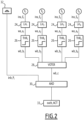
- FIG. 2 illustrates a functional diagram 120 of an example of a control-command application to be executed.
- Such an application corresponds to the detection of the temperature limit at four distinct points of a nuclear reactor.
- Such an application is generated by an operator from a graphics editor connected to the automatic generator 110 of application program 34 without requiring any particular knowledge of VHDL or Verilog hardware description language.
- the automatic generator 110 of application program 34 is capable of converting the data of such a functional diagram 120 by the generator 110 of application program 34 into at least one sequence 46 of functional blocks to be executed, each functional block of the sequence implementing the functions conform to those previously programmed and listed in library file 100.
- the operator graphically defines the number of input signals to the control application, namely E1, E2, E3, and E4 which correspond, for example to different measurement points of a nuclear reactor.
- the electrical signals of the points Ei are then each capable of being converted by means of a functional block of the LIN type into physical data, here a temperature.
- the temperature obtained at the output of the functional block 24 of the LIN type is compared to a temperature threshold by means of a functional block 26 of the THR type having as parameter this temperature threshold, namely for example 100°C.
- the targeted control application then includes a voting function implemented by functional block 28 VOTER applied to the four signals associated with each entry point.
- the voting function is for example a 2/4 voting function capable of confirming or denying (i.e. binary result) the comparison to the temperature threshold, from the moment when at least two comparisons out of four have the same result.
- the targeted control application is capable of taking into account, by means of a functional block 30 AND, the activation of a push button 32 (capable of being activated manually by an operator) inhibiting the result.
- the functional block 30 AND receives two binary inputs corresponding respectively to the output signals of the push button 32 and the functional block 28 VOTER and outputs the binary result 33 of the functional block VOTER if the push button 32 does not was not activated, and the opposite binary result 33 otherwise.
- the library file 100 used by the automatic generator 110 is for example in the form of the following table:
- Kind Arbitrary code of the FB Function description Starters Exits Settings LINEN 0x01 Linear conversion of an electrical signal into physical data 1 analog 1 analog none THR 0x02 Comparison to a threshold value 1 analog 1 binary 1 analog: threshold value VOTE 0x03 2/4 voting function 4 binaries 1 binary none AND 0x04 Logical “AND” function between two inputs 2 binaries 1 binary none
- the memory 38 of the functional unit 14 comprises at least two data storage spaces 48 and 50 dedicated respectively to binary data (booleans coded on two distinct bits) and to analog data (floating numbers coded for example on thirty-two bits).
- the memory 38 of the functional unit 14 further comprises a data storage space dedicated to the parameter values of the file 40.
- the binary data storage space 48 is itself hierarchical into at least three subspaces, namely: a first subspace 52 dedicated to the binary input data of the programmable logic circuit 10, a second subspace 54 dedicated to temporary binary data obtained during execution of the sequence 46, a third subspace 56 dedicated to the binary output data of the programmable logic circuit.
- the analog data storage space 50 is itself hierarchical into at least three subspaces, namely: a first subspace 58 dedicated to the analog input data of the programmable logic circuit 10, a second subspace -space 60 dedicated to temporary analog data obtained during execution of sequence 46, a third subspace 62 dedicated to analog output data from the programmable logic circuit.
- the configuration file 36 of the memory 38 is configured to be read by the execution module 22 of the functional unit 14 during a single execution cycle of the control-command application (corresponding for example to that shown on the figure 2 ).
- the execution module 22 reads from the configuration file 36 where the values of the inputs and outputs of the application as a whole are stored in the memory 38.
- the configuration file 36 is an allocation table, in the different memory subspaces (i.e. registers), of memory addresses to the inputs and outputs of the programmable logic circuit 10.
- the five input values are, according to the example of control application shown on the figure 2 , to four analog values ina_E1, _ina_E2, ina_E3 and ina_E4 corresponding to the electrical signals representative of temperature measurements respectively at points E1 to E4 and a binary value inb_P1 representative of the activation/deactivation of the push button 32.
- the output value outb_ACT is delivered after execution of the functional blocks according to the sequence 46 of functional blocks.
- the configuration file 36 is, for example, in the form of the following table: Storage space type Analog 50 Binary 48 Subspace Entry 58 Entry 52 Exit 56 Memory address(es) 0x0001 to 0x0004 0x0005 to 0x0008 0x0009 to 0x0012 0x0013 to 0x0014 0x0000 0xF800 Value name ina_E1 ina_E2 ina_E3 ina_E4 inb_P1 outb_ACT
- the sequence 46 of functional block(s) to be executed is a computer file listing, from the causal links of the diagram, the order of instantiation of the functional blocks to be executed in series by the module execution 22 of the functional unit 14 to carry out the desired control application.
- Sequence 46 is a computer file, for example, represented in the form of the following ordered table: FB CODE FB_TYPE Instance 0x01 LINEN LIN 1 0x02 THR THR 1 0x01 LINEN LIN 2 0x02 THR THR 2 0x01 LINEN LIN 3 0x02 THR THR3 0x01 LINEN LIN 4 0x02 THR THR4 0x03 VOTE VOTE 0x04 AND AND 0x00 STOP STOP
- a single functional block FB (the code of which is indicated in the library file previously described) is executed at a time, according to the successive instances of the series of functional blocks indicated in the sequence computer file 46 ci -above.
- the FPGA includes four LIN type functional blocks, four THR type functional blocks, one VOTER type functional block and one AND type functional block, making a total of approximately ten distinct functional blocks.
- the present invention only one functional block of each type is necessary and “called” as many times as required according to the control application to be executed.
- the number of functional blocks necessary to execute such an application is reduced from ten to four, which allows a reduction in the size of the FPGA (ie optimization of the compactness) and/or the possibility of integrating functional blocks that can be called for other control applications.
- the hardware footprint (e.g. VHDL footprint) of the programmable logic circuit according to the invention is unique and permanent, a qualified functional block being suitable for being reused from one control application to another.
- the application program 34 is distinct from one control application to another, the same functional block being for example called in the first instance for a first control application and in the last instance for a second application. control command different from the first.
- the computer file 40 of parameter value(s) of functional blocks(s) comprises the values of the parameters necessary during the execution of the sequence 46, these parameter values being ordered taking into account the sequence 46 execution of functional blocks.
- the computer file 40 of parameter values is represented, for example in the form of the following ordered table: Parameter value Function block instance Parameter value 0x0000000042c80000 THR 1 100.0 0x0000000042c80000 THR 2 100.0 0x0000000042c80000 THR3 100.0 0x0000000042c80000 THR4 100.0
- the present invention allows a change of parameter of the same functional block during the life of a control system. , or from one application to another. The evolution of the operation of the programmable circuit is therefore facilitated.
- the application program 34 also includes two computer files 42 and 44 listing respectively for each functional block on the one hand the address(es) of the memory 38 allocated to one or more input operands of this functional block, and on the other hand the address(es) of the memory allocated to one or more output operands of this functional block.
- these two computer files 42 and 44 are, for example, respectively in the following form: Memory address(es) Input value name Used as an input to: Memory address(es) Output value name Used at the output of: 0x0001 ina_E1 LINEN 0x0800 wa_a1 LINEN 0x0800 wa_a1 THR 0x0804 wa_b1 THR 0x0005 ina_E2 LINEN 0x0805 wa_a2 LINEN 0x0805 wa_a2 THR 0x0809 wb_b2 THR 0x0009 ina_E3 LINEN 0x080A wa_a3 LINEN 0x080A wa_a3 THR 0x080E wb_b3 THR 0x0013 ina_E4 LINEN 0x080F wa_a4 LINEN 0x080F wa_a4 LINEN 0x080F wa_a4 THR 0x0813
- the execution module 22 then functions as a state machine and automatically distributes and/or stores to each functional block instance the input and output values at the memory addresses indicated in the files 42 and 44 of the application program 34.
- a pointer allows the execution module 22 to know for each functional block instance the starting location of the addresses of the input and output values to read in the files 42 and 44. At the end of the execution of each functional block instance, it updates the pointer according to the number of input values read and the number of output values generated, allowing the execution module 22 to know the addresses to read in the files 42 and 44 for the next block instance.
- the computer files of the application program 34 have a synergistic effect so that the execution module 22 is configured for all take into account in parallel in order to implement serial execution without any link being physically created between the different functional blocks.
- the execution module 22 is configured to read the sequence 46 and determine which is the first functional block to execute.
- This first block is the functional block FB, of the LIN type, and the execution module 22 is then configured to distribute as input, in accordance with the computer file 42 associated with the input data of each functional block, the analog value of ina_E1 which is stored at address 0x0001 of subspace 58 dedicated to the analog input data of memory 38.
- the functional block FB of the LIN type, is then executed and the analog value of wa_a1 delivered as output is stored at address 0x0800 of the memory subspace 60 dedicated to temporary analog data in accordance with the computer file 44 associated with the output data of each functional block.
- the THR type functional block FB 5 is then executed and the binary value of wb_b1 delivered as output is written and stored by the execution module 22 at address 0x0804 of the subspace 54 dedicated to temporary binary data.
- the third functional block to be executed is again the functional block FB, of type LIN.
- the execution module 22 is then configured to distribute as input the analog value of ina_E2 which is stored at address 0x0005 of subspace 58 dedicated to data analog input from memory 38.
- the FB functional block, of the LIN type is then executed for the second time and the analog value of wa_a2 delivered at the output is stored at address 0x0805 of the memory subspace 60 dedicated to temporary analog data, and so on until until the entire sequence 46 is completely executed (i.e. until the stop code 0x00 is read by the execution module 22).
- the functional unit 14 further comprises a plurality 64 of M parallelizable floating point units (FPU), with M an integer.
- FPU parallelizable floating point units
- Such calculation units are for example suitable for implementing square root or logarithm calculations and are parallelized, for the implementation of complex calculations required during the execution of a functional block such as the determination of the ratio between the heat flux at the onset of the boiling crisis and the actual heat flux in the core of a reactor called critical heat flux ratio/RFTC (DBNR from English Departure from Nucleate Boiling Ratio ) .
- DBNR critical heat flux ratio/RFTC
- Such a pool of floating point calculation units is shared for all the functional blocks of the functional unit 14 and makes it possible to accelerate the calculation capacity of a functional block when it is configured to perform a calculation. complex analog. The scalability of the programmable logic circuit 10 is consequently increased.
- the functional unit 14 also includes an input-output interface 66 capable of receiving and retransmitting respectively the input data ina_E1, ina_E2, ina_E3, ina_E4 and output data inb_P1 and outb_ACT listed in the configuration file 36, and associated with the control application as a whole.
- the interface 66 is suitable for receiving the application program 34 via an internal configuration bus (ICB) connected to the input signal control module 12 and for transmitting data via this same data bus. control and diagnostics to the module 16 for controlling the output signals.
- ICB internal configuration bus
- the module 12 for controlling the input signals like the module 16 for controlling the output signals are external to the functional unit 14 and are capable of communicating with devices and/or circuits external to the programmable logic circuit 10.
- This input signal control module 12 and this output signal control module 16 are themselves each a state machine comprising one or more memory spaces dedicated respectively to analog and binary data not shown.
- these dedicated memory spaces some are dedicated to the control of input and output data exchanged with a communication network and suitable for receiving/transmitting data transmitted/transmitted asynchronously with regard to the operating cycle of the programmable logic circuit 10
- these memory spaces dedicated specifically to network data are synchronous flip-flop register(s) (ie double-port, English flip-flop ) so as to store the network data received/transmitted during the current cycle while the network data received/transmitted during the previous cycle are used by the functional unit 14 during the current cycle.
- the programmable logic circuit 10 therefore has a certain number of optical fiber connectors making it possible to transmit/receive this data on communication networks.
- Modules 12 and 16 are in particular configured to ensure communication with a maintenance and diagnostic module 68 (SMD from English Service Maintenance Diagnosis Module ) shown on the Figure 3 .
- SMD Service Maintenance Diagnosis Module
- Such a maintenance and diagnostic module 68 makes it possible in particular to load, on the programmable logic circuit 10, the application program 34 associated with the application to be executed or even changes in functional block parameters (eg a change in temperature threshold of 100°C to 120°C), to periodically launch maintenance tests on the programmable logic circuit 10, or to transfer processing data from the programmable logic circuit 10 according to the invention to the maintenance and diagnostic module 68.
- These data exchanges between the programmable logic circuit 10 and the maintenance and diagnostic module 68 are secured by means of a connection such as a bus 70 connected to the rear face (from the English backplane bus ) of the boxes respectively housing the programmable logic circuit 10 and the maintenance and diagnostic module 68.
- the maintenance and diagnostic module 68 also includes a programmable logic circuit 72, for example FPGA and a microprocessor 74, and is capable of communicating according to a secure procedure with a maintenance center 76 comprising, for example, the automatic generator 110, at means of an Ethernet type connection 78 and a switch 80 capable of communicating with other electrical installation control devices, a control device comprising at least one programmable logic circuit 10 according to the invention as described above.
- a programmable logic circuit 72 for example FPGA and a microprocessor 74
- the maintenance and diagnostic module 68 also includes a programmable logic circuit 72, for example FPGA and a microprocessor 74, and is capable of communicating according to a secure procedure with a maintenance center 76 comprising, for example, the automatic generator 110, at means of an Ethernet type connection 78 and a switch 80 capable of communicating with other electrical installation control devices, a control device comprising at least one programmable logic circuit 10 according to the invention as described above.
- the maintenance center 76 is, for example, distant from the nuclear electrical installation on which the programmable logic circuit 10 is implemented. Within this maintenance center 76, a maintenance operator uses a graphic editor (not requiring prior knowledge of VHDL or Verilog) to carry out the control applications to be implemented within the installation. Nuclear electric, in the form of functional diagrams 120 as represented for example, on the figure 2 . As indicated previously, the functional diagrams 120 are then converted into application program 34, by the automatic generator 110 which uses the library file 100 to guarantee that the program application program 34 will execute without affecting the qualified configuration of the programmable logic circuit 10. The application program 34 is then loaded via the maintenance and diagnostic module 68 into the programmable logic circuit 10.
- the control device 81 is a “mono-” programmable logic circuit 10.
- the control device 81 comprises a housing 82 (from the English rack ) forming a box, for example of size 6U (U being l 'unit of height of a rack), in which a single programmable logic circuit 10 is integrated.
- Housing 82 is capable of further comprising a power supply module 84, and auxiliary modules, namely one or more modules 86 dedicated to the acquisition of distinct input data, and one or more modules 88 dedicated to publication of distinct output data, and one or more maintenance and diagnostic modules 68 previously described.
- the programmable logic circuit 10 comprises connectors (for example seven connectors not shown) allowing, for example by means of optical fiber(s), a connection to a communication network.
- a connection of the automatic generator 110 of application program 34 to the control device 81 is capable of being established via the maintenance and diagnostic module(s) 68, which is in particular configured to load the sequence 46 of functional blocks to be executed in the control device 81 once such a connection is established.
- programmable logic circuit 10 is master and controls communication with auxiliary modules 86, 88, and 68 through a bus 70 using, for example, non-limiting low voltage differential transmission links (M-LVDS from English Multipoint-Low Voltage Differential Signaling ), operating for example at 50MHz, and dedicated respectively to the binary and analog input data and to the binary and analog output data of the programmable logic circuit 10.
- M-LVDS non-limiting low voltage differential transmission links
- each type of data input or output
- modules 86 dedicated to the acquisition of input data, and the modules 88 dedicated to the publication of output data could be housed on the same electronic card of the "GPIO" type (from the English general purpose input output ) known elsewhere.
- the power module 84 delivers a stabilized power supply to the other modules of the housing 82 and is also configured to implement a voltage conversion, for example from 24 volts to direct current to 5 volts to power each module of the housing 82.
- THE figures 5 And 6 represent two variants of control devices 81 comprising a plurality of programmable logic circuits 10 represented in figure 1 .
- Such a “multi-” programmable logic circuit architecture 10 makes it possible to increase the number of network interfaces per control device, to duplicate control operations in at least two programmable logic circuits 10 for security control purposes imposing requirements. redundancy rules, or even optimize inter-module routing within a housing 82.
- the plurality of programmable logic circuits 10 is synchronized, this synchronization is carried out via a master logic circuit 10a among the programmable logic circuits 10, connected to a clock.
- the master programmable logic circuit 10a is particularly capable of transmitting, via the signal control module 12 shown on the figure 1 , a synchronization pulse at the start and/or end of the cycle (a cycle having for example a duration of 2ms) and a status request to the modules 86 dedicated to distinct input data, the modules 88 dedicated to distinct output data, or to the other programmable logic circuits 10 in order to synchronize and refresh the input/output data of the following cycle at each cycle (new iteration of the same control application). Consequently, unlike exchanges via communication networks, these data exchanges within the same plurality of programmable logic circuits are carried out in a synchronous mode.
- all the programmable logic circuits 10 of the plurality are configured to operate simultaneously within the same cycle.
- three programmable logic circuits comprising a master programmable logic circuit 10a and two other programmable logic circuits 10, are housed in the same housing 82, the programmable logic circuits 10 and 10a, being able to communicate with each other and with the auxiliary modules 86 , 88, 68 of housing 82 synchronously.
- the programmable logic circuits 10a and 10 communicate with each other in a manner synchronous by optical fiber 92, connectors being specifically dedicated to this programmable logic inter-circuit communication within a “multi-” - circuit architecture.
- the master programmable logic circuit 10a communicates synchronously with the auxiliary modules 86, 88, 68 of the housing 82 by means of the bus 70.
- each housing 90A, 90B, 90C corresponds to an arrangement described in the Figure 4 (Single-Circuit) or in the Figure 5 (Multi-Circuit).
- Each housing may also include auxiliary modules 86, 88, 68.
- one of the housings 90A is “master” and comprises the master programmable logic circuit 10a for all of the programmable logic circuits 10 of the multi-circuit and multi-housing control device 81, and ensuring the synchronization of the auxiliary modules 86 , 88, 68 from your accommodation via the 70A bus.
- the programmable logic circuits 10 of the control device 81 are capable of communicating from one housing to another and within the same housing synchronously by optical fiber 92.
- Each “slave” housing 90B, 90C of the master housing 90A includes among its programmable logic circuits 10 a programmable sychonization logic circuit 10b to synchronize the auxiliary modules 86, 88, 68 of its housing via the bus 70B, 70C of the housing
- a single maintenance and diagnostic module 68 is implemented per control device 81, independently of the number of programmable logic circuit(s). s) 10 or the number of dwelling(s) it includes.
- a bus 70A, 70B, 70C advantageously comprises four connection links low voltage differential transmission (M-LVDS from English Multipoint-Low Voltage Differential Signaling ), operating for example at 50MHz. in each direction of transmission.
- buses 70A, 70B, 70C can be dimensioned to allow each programmable logic circuit 10 to be connected to the auxiliary modules 86, 88, 68 of its housing through the bus 70A, 70B, 70C.
Landscapes
- Physics & Mathematics (AREA)
- Engineering & Computer Science (AREA)
- Mathematical Physics (AREA)
- General Engineering & Computer Science (AREA)
- Computer Hardware Design (AREA)
- Computing Systems (AREA)
- High Energy & Nuclear Physics (AREA)
- Plasma & Fusion (AREA)
- Computer Security & Cryptography (AREA)
- Computer Networks & Wireless Communication (AREA)
- Programmable Controllers (AREA)
- Logic Circuits (AREA)
- Microcomputers (AREA)
Priority Applications (2)
| Application Number | Priority Date | Filing Date | Title |
|---|---|---|---|
| RS20240368A RS65358B1 (sr) | 2017-03-08 | 2018-03-08 | Programabilno logičko kolo za upravljanje električnim postrojenjem, određenije nuklearnim postrojenjem, i pridruženi uređaj |
| HRP20240326TT HRP20240326T1 (hr) | 2017-03-08 | 2018-03-08 | Programibilni logički krug za upravljanje električnim postrojenjem, točnije nuklearnim postrojenjem i odgovarajući kontrolni uređaj |
Applications Claiming Priority (2)
| Application Number | Priority Date | Filing Date | Title |
|---|---|---|---|
| FR1751903A FR3063855B1 (fr) | 2017-03-08 | 2017-03-08 | Circuit logique programmable de commande d'une installation electrique, en particulier une installation nucleaire, dispositif et procede de commande associes |
| PCT/EP2018/055817 WO2018162668A1 (fr) | 2017-03-08 | 2018-03-08 | Circuit logique programmable de commande d'une installation électrique, en particulier une installation nucléaire, dispositif et procédé de commande associés |
Publications (2)
| Publication Number | Publication Date |
|---|---|
| EP3593360A1 EP3593360A1 (fr) | 2020-01-15 |
| EP3593360B1 true EP3593360B1 (fr) | 2024-01-03 |
Family
ID=59253631
Family Applications (1)
| Application Number | Title | Priority Date | Filing Date |
|---|---|---|---|
| EP18708146.8A Active EP3593360B1 (fr) | 2017-03-08 | 2018-03-08 | Circuit logique programmable de commande d'une installation électrique, en particulier une installation nucléaire et dispositif associé |
Country Status (17)
| Country | Link |
|---|---|
| US (1) | US11043949B2 (pl) |
| EP (1) | EP3593360B1 (pl) |
| JP (1) | JP7282038B2 (pl) |
| KR (1) | KR102471141B1 (pl) |
| CN (1) | CN110520936B (pl) |
| BR (1) | BR112019018565B1 (pl) |
| CA (1) | CA3055466A1 (pl) |
| ES (1) | ES2974420T3 (pl) |
| FR (1) | FR3063855B1 (pl) |
| HR (1) | HRP20240326T1 (pl) |
| HU (1) | HUE066193T2 (pl) |
| PL (1) | PL3593360T3 (pl) |
| RS (1) | RS65358B1 (pl) |
| RU (1) | RU2769961C2 (pl) |
| UA (1) | UA125309C2 (pl) |
| WO (1) | WO2018162668A1 (pl) |
| ZA (1) | ZA201905889B (pl) |
Families Citing this family (8)
| Publication number | Priority date | Publication date | Assignee | Title |
|---|---|---|---|---|
| US11017907B2 (en) * | 2013-12-31 | 2021-05-25 | Nuscale Power, Llc | Nuclear reactor protection systems and methods |
| KR102873531B1 (ko) | 2016-12-30 | 2025-10-17 | 뉴스케일 파워, 엘엘씨 | 핵 반응기 보호 시스템 및 방법 |
| JP6954190B2 (ja) * | 2018-03-12 | 2021-10-27 | オムロン株式会社 | 制御システム、コントローラ、および制御方法 |
| JP7091986B2 (ja) * | 2018-10-05 | 2022-06-28 | オムロン株式会社 | 制御システム、制御方法、および開発支援プログラム |
| EP4016935A1 (en) * | 2020-12-15 | 2022-06-22 | Schneider Electric Industries SAS | Multipoint ethernet bus |
| CN116088405B (zh) * | 2022-12-28 | 2025-05-30 | 青岛华晟智能装备股份有限公司 | 输送管理方法、设备、输送系统及存储介质 |
| JP2024095855A (ja) * | 2022-12-29 | 2024-07-11 | Awl株式会社 | パイプライン処理システム、及びパイプライン処理プログラム |
| CN119718217B (zh) * | 2025-02-28 | 2025-05-23 | 苏州元脑智能科技有限公司 | 芯片物理信息获取方法、装置、电子设备及存储介质 |
Family Cites Families (22)
| Publication number | Priority date | Publication date | Assignee | Title |
|---|---|---|---|---|
| RU2117978C1 (ru) * | 1996-09-24 | 1998-08-20 | Борис Германович Терехин | Программируемое устройство для логического управления электроприводами и сигнализацией |
| WO2000036492A2 (en) * | 1998-12-18 | 2000-06-22 | Triconex Corporation | Method and apparatus for processing control using a multiple redundant processor control system |
| JP3743487B2 (ja) * | 1999-07-14 | 2006-02-08 | 富士ゼロックス株式会社 | プログラマブル論理回路装置、情報処理システム、プログラマブル論理回路装置への回路の再構成方法、プログラマブル論理回路装置用の回路情報の圧縮方法 |
| KR100399759B1 (ko) * | 2000-11-01 | 2003-09-29 | 한국과학기술원 | 원자력 발전소의 디지털 온라인 능동 시험 발전소 보호시스템 및 그 방법 |
| GB2374242B (en) * | 2001-04-07 | 2005-03-16 | Univ Dundee | Integrated circuit and related improvements |
| TWI234737B (en) * | 2001-05-24 | 2005-06-21 | Ip Flex Inc | Integrated circuit device |
| US6842669B2 (en) * | 2001-09-24 | 2005-01-11 | Westinghouse Electric Company Llc | Component interface module |
| US8109766B2 (en) * | 2003-10-03 | 2012-02-07 | Global Nuclear Fuel-Americas Llc | Method for predicted reactor simulation |
| JP4095576B2 (ja) * | 2004-05-17 | 2008-06-04 | 株式会社東芝 | プログラマブル論理回路を用いる汎用論理回路装置 |
| JP4442524B2 (ja) * | 2005-07-12 | 2010-03-31 | 株式会社ジェイテクト | 安全plc |
| US7725519B2 (en) * | 2005-10-05 | 2010-05-25 | Qualcom Incorporated | Floating-point processor with selectable subprecision |
| US7870299B1 (en) * | 2008-02-06 | 2011-01-11 | Westinghouse Electric Co Llc | Advanced logic system |
| US8040151B2 (en) * | 2008-12-19 | 2011-10-18 | Actel Corporation | Programmable logic device with programmable wakeup pins |
| JP2010226524A (ja) * | 2009-03-24 | 2010-10-07 | Fuji Xerox Co Ltd | プログラマブル論理回路、半導体集積回路装置、情報処理システムおよび制御プログラム |
| US8347044B2 (en) * | 2009-09-30 | 2013-01-01 | General Electric Company | Multi-processor based programmable logic controller and method for operating the same |
| JP5818762B2 (ja) * | 2012-09-14 | 2015-11-18 | 株式会社東芝 | プログラマブルロジックデバイス及びその検証方法 |
| US8694951B1 (en) * | 2012-10-02 | 2014-04-08 | Lsi Corporation | Core wrapping in the presence of an embedded wrapped core |
| JP2014225164A (ja) | 2013-05-16 | 2014-12-04 | 富士通株式会社 | 伝送装置 |
| US11017907B2 (en) * | 2013-12-31 | 2021-05-25 | Nuscale Power, Llc | Nuclear reactor protection systems and methods |
| EP2988420B1 (en) | 2014-08-20 | 2021-03-10 | Framatome | Circuit arrangement for a safety i&c system |
| EP3082133B1 (en) * | 2015-04-14 | 2023-06-07 | General Electric Technology GmbH | Nuclear instrumentation and control system |
| PL3107212T3 (pl) * | 2015-06-16 | 2018-10-31 | Framatome | Bezpośrednio programowalna macierz bramek zawierająca wiele bloków funkcjonalnych oraz urządzenie sterujące dla elektrowni |
-
2017
- 2017-03-08 FR FR1751903A patent/FR3063855B1/fr active Active
-
2018
- 2018-03-08 HR HRP20240326TT patent/HRP20240326T1/hr unknown
- 2018-03-08 JP JP2019548580A patent/JP7282038B2/ja active Active
- 2018-03-08 RS RS20240368A patent/RS65358B1/sr unknown
- 2018-03-08 RU RU2019128044A patent/RU2769961C2/ru active
- 2018-03-08 WO PCT/EP2018/055817 patent/WO2018162668A1/fr not_active Ceased
- 2018-03-08 EP EP18708146.8A patent/EP3593360B1/fr active Active
- 2018-03-08 CA CA3055466A patent/CA3055466A1/fr active Pending
- 2018-03-08 ES ES18708146T patent/ES2974420T3/es active Active
- 2018-03-08 PL PL18708146.8T patent/PL3593360T3/pl unknown
- 2018-03-08 KR KR1020197028562A patent/KR102471141B1/ko active Active
- 2018-03-08 HU HUE18708146A patent/HUE066193T2/hu unknown
- 2018-03-08 CN CN201880022058.2A patent/CN110520936B/zh active Active
- 2018-03-08 BR BR112019018565-8A patent/BR112019018565B1/pt active IP Right Grant
- 2018-03-08 US US16/492,112 patent/US11043949B2/en active Active
- 2018-03-08 UA UAA201909682A patent/UA125309C2/uk unknown
-
2019
- 2019-09-06 ZA ZA2019/05889A patent/ZA201905889B/en unknown
Also Published As
| Publication number | Publication date |
|---|---|
| ES2974420T3 (es) | 2024-06-27 |
| EP3593360A1 (fr) | 2020-01-15 |
| CN110520936A (zh) | 2019-11-29 |
| JP7282038B2 (ja) | 2023-05-26 |
| JP2020515130A (ja) | 2020-05-21 |
| BR112019018565A2 (pt) | 2020-04-14 |
| RU2019128044A3 (pl) | 2021-05-06 |
| FR3063855B1 (fr) | 2019-04-12 |
| PL3593360T3 (pl) | 2024-05-27 |
| CN110520936B (zh) | 2023-04-18 |
| US11043949B2 (en) | 2021-06-22 |
| KR20190127773A (ko) | 2019-11-13 |
| HRP20240326T1 (hr) | 2024-06-21 |
| WO2018162668A1 (fr) | 2018-09-13 |
| CA3055466A1 (fr) | 2018-09-13 |
| RU2769961C2 (ru) | 2022-04-11 |
| US20210083671A1 (en) | 2021-03-18 |
| KR102471141B1 (ko) | 2022-11-28 |
| FR3063855A1 (fr) | 2018-09-14 |
| ZA201905889B (en) | 2020-06-24 |
| RU2019128044A (ru) | 2021-03-09 |
| RS65358B1 (sr) | 2024-04-30 |
| BR112019018565B1 (pt) | 2023-11-07 |
| UA125309C2 (uk) | 2022-02-16 |
| HUE066193T2 (hu) | 2024-07-28 |
Similar Documents
| Publication | Publication Date | Title |
|---|---|---|
| EP3593360B1 (fr) | Circuit logique programmable de commande d'une installation électrique, en particulier une installation nucléaire et dispositif associé | |
| EP0063071B1 (fr) | Procédé et dispositif de transmission de données numériques | |
| EP3189380A1 (fr) | Architecture bi-voies avec liaisons ccdl redondantes | |
| WO1998038553A1 (fr) | Architecture modulaire de pilotage d'un aerodyne presentant un faible cout tout en etant apte a assurer un niveau eleve de securite de fonctionnement | |
| FR2728749A1 (fr) | Procede de commande d'un sous-systeme d'exploitation et de gestion pour un systeme n[1 d'echange de messages de signalisation | |
| EP3189381A1 (fr) | Architecture bi-voies | |
| WO2020188178A1 (fr) | Systeme de commande d'un reseau electrique d'avion | |
| FR2684211A1 (fr) | Dispositif d'exploitation des informations relatives aux pannes detectees par une ou plusieurs unites centrales d'un aeronef. | |
| FR2712998A1 (fr) | Simulateur de bus numériques intégré dans un système de test automatique de boîtiers électroniques embarqués sur avion. | |
| EP1372074B1 (fr) | Procédé et système de gestion des événements | |
| EP1998257B1 (fr) | Dispositif de contrôle de communication point à point entre un module et un bus de transmission | |
| EP2916220A1 (fr) | Système électronique comprenant des dispositifs électroniques, disjoncteur comportant un tel système, procédé de génération d'un indicateur d'écart en cas d'incompatibilité entre dispositifs et produit programme d'ordinateur associé | |
| EP1998256B1 (fr) | Dispositif de contrôle de communication entre un module et un bus de transmission | |
| EP0589743B1 (fr) | Dispositif modulaire permettant le couplage et le multiplexage de bus de différents types | |
| WO2014202635A1 (fr) | Procédé de communication dans un réseau interconnectant au moins deux groupes électrogènes, et dispositif d'interfaçage correspondant | |
| EP0245152B1 (fr) | Processeur de calcul de la transformée de Fourier discrète comportant un dispositif de test en ligne | |
| EP2217974A1 (fr) | Module d'entrées/sorties intégrant une fonction logique pour contrôler les données | |
| FR2572203A1 (fr) | Procede et appareil pour systemes distants extensibles de teletraitement a interface | |
| EP0344052A1 (fr) | Mémoire modulaire | |
| CN112421783B (zh) | 多状态量可组态变电设备智能组件 | |
| RU147249U1 (ru) | Измерительный терминал для систем измерений электрических параметров с гибким динамическим перераспределением функций между терминалами | |
| EP4449208A1 (fr) | Système pour la conduite et l'aide à la conduite d'un processus industriel critique et procédé associé | |
| CN113849375A (zh) | 一种用于计算机的远程管理方法、系统及介质 | |
| FR3102282A1 (fr) | Procédé d’échange de données entre des entités et un système de mesure | |
| FR2993427A1 (fr) | Module de surveillance de defauts a l'armoire d'eclairage public. |
Legal Events
| Date | Code | Title | Description |
|---|---|---|---|
| STAA | Information on the status of an ep patent application or granted ep patent |
Free format text: STATUS: UNKNOWN |
|
| STAA | Information on the status of an ep patent application or granted ep patent |
Free format text: STATUS: THE INTERNATIONAL PUBLICATION HAS BEEN MADE |
|
| PUAI | Public reference made under article 153(3) epc to a published international application that has entered the european phase |
Free format text: ORIGINAL CODE: 0009012 |
|
| STAA | Information on the status of an ep patent application or granted ep patent |
Free format text: STATUS: REQUEST FOR EXAMINATION WAS MADE |
|
| 17P | Request for examination filed |
Effective date: 20190905 |
|
| AK | Designated contracting states |
Kind code of ref document: A1 Designated state(s): AL AT BE BG CH CY CZ DE DK EE ES FI FR GB GR HR HU IE IS IT LI LT LU LV MC MK MT NL NO PL PT RO RS SE SI SK SM TR |
|
| AX | Request for extension of the european patent |
Extension state: BA ME |
|
| DAV | Request for validation of the european patent (deleted) | ||
| DAX | Request for extension of the european patent (deleted) | ||
| STAA | Information on the status of an ep patent application or granted ep patent |
Free format text: STATUS: EXAMINATION IS IN PROGRESS |
|
| 17Q | First examination report despatched |
Effective date: 20211027 |
|
| REG | Reference to a national code |
Ref country code: DE Free format text: PREVIOUS MAIN CLASS: G21D0003000000 Ref country code: DE Ref legal event code: R079 Ref document number: 602018063555 Country of ref document: DE Free format text: PREVIOUS MAIN CLASS: G21D0003000000 Ipc: H03K0019177640 |
|
| P01 | Opt-out of the competence of the unified patent court (upc) registered |
Effective date: 20230606 |
|
| RIC1 | Information provided on ipc code assigned before grant |
Ipc: G21D 3/00 20060101ALI20230621BHEP Ipc: H03K 19/17768 20200101ALI20230621BHEP Ipc: H03K 19/17764 20200101AFI20230621BHEP |
|
| GRAP | Despatch of communication of intention to grant a patent |
Free format text: ORIGINAL CODE: EPIDOSNIGR1 |
|
| STAA | Information on the status of an ep patent application or granted ep patent |
Free format text: STATUS: GRANT OF PATENT IS INTENDED |
|
| INTG | Intention to grant announced |
Effective date: 20230802 |
|
| GRAS | Grant fee paid |
Free format text: ORIGINAL CODE: EPIDOSNIGR3 |
|
| GRAA | (expected) grant |
Free format text: ORIGINAL CODE: 0009210 |
|
| STAA | Information on the status of an ep patent application or granted ep patent |
Free format text: STATUS: THE PATENT HAS BEEN GRANTED |
|
| AK | Designated contracting states |
Kind code of ref document: B1 Designated state(s): AL AT BE BG CH CY CZ DE DK EE ES FI FR GB GR HR HU IE IS IT LI LT LU LV MC MK MT NL NO PL PT RO RS SE SI SK SM TR |
|
| REG | Reference to a national code |
Ref country code: GB Ref legal event code: FG4D Free format text: NOT ENGLISH |
|
| REG | Reference to a national code |
Ref country code: CH Ref legal event code: EP |
|
| REG | Reference to a national code |
Ref country code: DE Ref legal event code: R096 Ref document number: 602018063555 Country of ref document: DE |
|
| REG | Reference to a national code |
Ref country code: IE Ref legal event code: FG4D Free format text: LANGUAGE OF EP DOCUMENT: FRENCH |
|
| REG | Reference to a national code |
Ref country code: LT Ref legal event code: MG9D |
|
| PGFP | Annual fee paid to national office [announced via postgrant information from national office to epo] |
Ref country code: CZ Payment date: 20240312 Year of fee payment: 8 |
|
| REG | Reference to a national code |
Ref country code: NL Ref legal event code: MP Effective date: 20240103 |
|
| REG | Reference to a national code |
Ref country code: SK Ref legal event code: T3 Ref document number: E 43779 Country of ref document: SK |
|
| REG | Reference to a national code |
Ref country code: HR Ref legal event code: ODRP Ref document number: P20240326T Country of ref document: HR Payment date: 20240308 Year of fee payment: 7 |
|
| REG | Reference to a national code |
Ref country code: GR Ref legal event code: EP Ref document number: 20240400795 Country of ref document: GR Effective date: 20240516 |
|
| REG | Reference to a national code |
Ref country code: AT Ref legal event code: MK05 Ref document number: 1647825 Country of ref document: AT Kind code of ref document: T Effective date: 20240103 |
|
| REG | Reference to a national code |
Ref country code: HR Ref legal event code: T1PR Ref document number: P20240326 Country of ref document: HR |
|
| PG25 | Lapsed in a contracting state [announced via postgrant information from national office to epo] |
Ref country code: NL Free format text: LAPSE BECAUSE OF FAILURE TO SUBMIT A TRANSLATION OF THE DESCRIPTION OR TO PAY THE FEE WITHIN THE PRESCRIBED TIME-LIMIT Effective date: 20240103 |
|
| REG | Reference to a national code |
Ref country code: ES Ref legal event code: FG2A Ref document number: 2974420 Country of ref document: ES Kind code of ref document: T3 Effective date: 20240627 |
|
| PG25 | Lapsed in a contracting state [announced via postgrant information from national office to epo] |
Ref country code: NL Free format text: LAPSE BECAUSE OF FAILURE TO SUBMIT A TRANSLATION OF THE DESCRIPTION OR TO PAY THE FEE WITHIN THE PRESCRIBED TIME-LIMIT Effective date: 20240103 |
|
| PG25 | Lapsed in a contracting state [announced via postgrant information from national office to epo] |
Ref country code: IS Free format text: LAPSE BECAUSE OF FAILURE TO SUBMIT A TRANSLATION OF THE DESCRIPTION OR TO PAY THE FEE WITHIN THE PRESCRIBED TIME-LIMIT Effective date: 20240503 |
|
| PG25 | Lapsed in a contracting state [announced via postgrant information from national office to epo] |
Ref country code: LT Free format text: LAPSE BECAUSE OF FAILURE TO SUBMIT A TRANSLATION OF THE DESCRIPTION OR TO PAY THE FEE WITHIN THE PRESCRIBED TIME-LIMIT Effective date: 20240103 |
|
| PG25 | Lapsed in a contracting state [announced via postgrant information from national office to epo] |
Ref country code: AT Free format text: LAPSE BECAUSE OF FAILURE TO SUBMIT A TRANSLATION OF THE DESCRIPTION OR TO PAY THE FEE WITHIN THE PRESCRIBED TIME-LIMIT Effective date: 20240103 |
|
| REG | Reference to a national code |
Ref country code: HU Ref legal event code: AG4A Ref document number: E066193 Country of ref document: HU |
|
| PG25 | Lapsed in a contracting state [announced via postgrant information from national office to epo] |
Ref country code: LT Free format text: LAPSE BECAUSE OF FAILURE TO SUBMIT A TRANSLATION OF THE DESCRIPTION OR TO PAY THE FEE WITHIN THE PRESCRIBED TIME-LIMIT Effective date: 20240103 Ref country code: IS Free format text: LAPSE BECAUSE OF FAILURE TO SUBMIT A TRANSLATION OF THE DESCRIPTION OR TO PAY THE FEE WITHIN THE PRESCRIBED TIME-LIMIT Effective date: 20240503 Ref country code: BG Free format text: LAPSE BECAUSE OF FAILURE TO SUBMIT A TRANSLATION OF THE DESCRIPTION OR TO PAY THE FEE WITHIN THE PRESCRIBED TIME-LIMIT Effective date: 20240103 Ref country code: AT Free format text: LAPSE BECAUSE OF FAILURE TO SUBMIT A TRANSLATION OF THE DESCRIPTION OR TO PAY THE FEE WITHIN THE PRESCRIBED TIME-LIMIT Effective date: 20240103 |
|
| PG25 | Lapsed in a contracting state [announced via postgrant information from national office to epo] |
Ref country code: PT Free format text: LAPSE BECAUSE OF FAILURE TO SUBMIT A TRANSLATION OF THE DESCRIPTION OR TO PAY THE FEE WITHIN THE PRESCRIBED TIME-LIMIT Effective date: 20240503 |
|
| PG25 | Lapsed in a contracting state [announced via postgrant information from national office to epo] |
Ref country code: SE Free format text: LAPSE BECAUSE OF FAILURE TO SUBMIT A TRANSLATION OF THE DESCRIPTION OR TO PAY THE FEE WITHIN THE PRESCRIBED TIME-LIMIT Effective date: 20240103 Ref country code: PT Free format text: LAPSE BECAUSE OF FAILURE TO SUBMIT A TRANSLATION OF THE DESCRIPTION OR TO PAY THE FEE WITHIN THE PRESCRIBED TIME-LIMIT Effective date: 20240503 Ref country code: LV Free format text: LAPSE BECAUSE OF FAILURE TO SUBMIT A TRANSLATION OF THE DESCRIPTION OR TO PAY THE FEE WITHIN THE PRESCRIBED TIME-LIMIT Effective date: 20240103 |
|
| REG | Reference to a national code |
Ref country code: DE Ref legal event code: R119 Ref document number: 602018063555 Country of ref document: DE |
|
| PG25 | Lapsed in a contracting state [announced via postgrant information from national office to epo] |
Ref country code: DK Free format text: LAPSE BECAUSE OF FAILURE TO SUBMIT A TRANSLATION OF THE DESCRIPTION OR TO PAY THE FEE WITHIN THE PRESCRIBED TIME-LIMIT Effective date: 20240103 |
|
| PG25 | Lapsed in a contracting state [announced via postgrant information from national office to epo] |
Ref country code: SM Free format text: LAPSE BECAUSE OF FAILURE TO SUBMIT A TRANSLATION OF THE DESCRIPTION OR TO PAY THE FEE WITHIN THE PRESCRIBED TIME-LIMIT Effective date: 20240103 |
|
| PG25 | Lapsed in a contracting state [announced via postgrant information from national office to epo] |
Ref country code: EE Free format text: LAPSE BECAUSE OF FAILURE TO SUBMIT A TRANSLATION OF THE DESCRIPTION OR TO PAY THE FEE WITHIN THE PRESCRIBED TIME-LIMIT Effective date: 20240103 |
|
| PG25 | Lapsed in a contracting state [announced via postgrant information from national office to epo] |
Ref country code: SM Free format text: LAPSE BECAUSE OF FAILURE TO SUBMIT A TRANSLATION OF THE DESCRIPTION OR TO PAY THE FEE WITHIN THE PRESCRIBED TIME-LIMIT Effective date: 20240103 Ref country code: EE Free format text: LAPSE BECAUSE OF FAILURE TO SUBMIT A TRANSLATION OF THE DESCRIPTION OR TO PAY THE FEE WITHIN THE PRESCRIBED TIME-LIMIT Effective date: 20240103 Ref country code: DK Free format text: LAPSE BECAUSE OF FAILURE TO SUBMIT A TRANSLATION OF THE DESCRIPTION OR TO PAY THE FEE WITHIN THE PRESCRIBED TIME-LIMIT Effective date: 20240103 |
|
| PLBE | No opposition filed within time limit |
Free format text: ORIGINAL CODE: 0009261 |
|
| STAA | Information on the status of an ep patent application or granted ep patent |
Free format text: STATUS: NO OPPOSITION FILED WITHIN TIME LIMIT |
|
| PG25 | Lapsed in a contracting state [announced via postgrant information from national office to epo] |
Ref country code: LU Free format text: LAPSE BECAUSE OF NON-PAYMENT OF DUE FEES Effective date: 20240308 |
|
| PG25 | Lapsed in a contracting state [announced via postgrant information from national office to epo] |
Ref country code: MC Free format text: LAPSE BECAUSE OF FAILURE TO SUBMIT A TRANSLATION OF THE DESCRIPTION OR TO PAY THE FEE WITHIN THE PRESCRIBED TIME-LIMIT Effective date: 20240103 |
|
| PG25 | Lapsed in a contracting state [announced via postgrant information from national office to epo] |
Ref country code: MC Free format text: LAPSE BECAUSE OF FAILURE TO SUBMIT A TRANSLATION OF THE DESCRIPTION OR TO PAY THE FEE WITHIN THE PRESCRIBED TIME-LIMIT Effective date: 20240103 Ref country code: LU Free format text: LAPSE BECAUSE OF NON-PAYMENT OF DUE FEES Effective date: 20240308 |
|
| PG25 | Lapsed in a contracting state [announced via postgrant information from national office to epo] |
Ref country code: IT Free format text: LAPSE BECAUSE OF FAILURE TO SUBMIT A TRANSLATION OF THE DESCRIPTION OR TO PAY THE FEE WITHIN THE PRESCRIBED TIME-LIMIT Effective date: 20240103 |
|
| 26N | No opposition filed |
Effective date: 20241007 |
|
| REG | Reference to a national code |
Ref country code: BE Ref legal event code: MM Effective date: 20240331 |
|
| PG25 | Lapsed in a contracting state [announced via postgrant information from national office to epo] |
Ref country code: IT Free format text: LAPSE BECAUSE OF FAILURE TO SUBMIT A TRANSLATION OF THE DESCRIPTION OR TO PAY THE FEE WITHIN THE PRESCRIBED TIME-LIMIT Effective date: 20240103 |
|
| PG25 | Lapsed in a contracting state [announced via postgrant information from national office to epo] |
Ref country code: DE Free format text: LAPSE BECAUSE OF NON-PAYMENT OF DUE FEES Effective date: 20241001 |
|
| PG25 | Lapsed in a contracting state [announced via postgrant information from national office to epo] |
Ref country code: BE Free format text: LAPSE BECAUSE OF NON-PAYMENT OF DUE FEES Effective date: 20240331 |
|
| PG25 | Lapsed in a contracting state [announced via postgrant information from national office to epo] |
Ref country code: DE Free format text: LAPSE BECAUSE OF NON-PAYMENT OF DUE FEES Effective date: 20241001 Ref country code: BE Free format text: LAPSE BECAUSE OF NON-PAYMENT OF DUE FEES Effective date: 20240331 |
|
| PGFP | Annual fee paid to national office [announced via postgrant information from national office to epo] |
Ref country code: HR Payment date: 20250326 Year of fee payment: 8 |
|
| REG | Reference to a national code |
Ref country code: HR Ref legal event code: ODRP Ref document number: P20240326 Country of ref document: HR Payment date: 20250326 Year of fee payment: 8 |
|
| PGFP | Annual fee paid to national office [announced via postgrant information from national office to epo] |
Ref country code: RO Payment date: 20250227 Year of fee payment: 8 |
|
| PGFP | Annual fee paid to national office [announced via postgrant information from national office to epo] |
Ref country code: HU Payment date: 20250228 Year of fee payment: 8 |
|
| PGFP | Annual fee paid to national office [announced via postgrant information from national office to epo] |
Ref country code: IE Payment date: 20250221 Year of fee payment: 8 |
|
| PGFP | Annual fee paid to national office [announced via postgrant information from national office to epo] |
Ref country code: NO Payment date: 20250228 Year of fee payment: 8 |
|
| PG25 | Lapsed in a contracting state [announced via postgrant information from national office to epo] |
Ref country code: SI Free format text: LAPSE BECAUSE OF FAILURE TO SUBMIT A TRANSLATION OF THE DESCRIPTION OR TO PAY THE FEE WITHIN THE PRESCRIBED TIME-LIMIT Effective date: 20240103 |
|
| PGFP | Annual fee paid to national office [announced via postgrant information from national office to epo] |
Ref country code: GR Payment date: 20250221 Year of fee payment: 8 |
|
| PGFP | Annual fee paid to national office [announced via postgrant information from national office to epo] |
Ref country code: FR Payment date: 20250331 Year of fee payment: 8 Ref country code: PL Payment date: 20250224 Year of fee payment: 8 |
|
| PGFP | Annual fee paid to national office [announced via postgrant information from national office to epo] |
Ref country code: SK Payment date: 20250221 Year of fee payment: 8 Ref country code: GB Payment date: 20250324 Year of fee payment: 8 |
|
| PGFP | Annual fee paid to national office [announced via postgrant information from national office to epo] |
Ref country code: RS Payment date: 20250228 Year of fee payment: 8 |
|
| PGFP | Annual fee paid to national office [announced via postgrant information from national office to epo] |
Ref country code: TR Payment date: 20250227 Year of fee payment: 8 |
|
| PGFP | Annual fee paid to national office [announced via postgrant information from national office to epo] |
Ref country code: AL Payment date: 20250321 Year of fee payment: 8 |
|
| PGFP | Annual fee paid to national office [announced via postgrant information from national office to epo] |
Ref country code: ES Payment date: 20250410 Year of fee payment: 8 |
|
| PGFP | Annual fee paid to national office [announced via postgrant information from national office to epo] |
Ref country code: CH Payment date: 20250401 Year of fee payment: 8 |
|
| PG25 | Lapsed in a contracting state [announced via postgrant information from national office to epo] |
Ref country code: CY Free format text: LAPSE BECAUSE OF FAILURE TO SUBMIT A TRANSLATION OF THE DESCRIPTION OR TO PAY THE FEE WITHIN THE PRESCRIBED TIME-LIMIT; INVALID AB INITIO Effective date: 20180308 |
|
| PG25 | Lapsed in a contracting state [announced via postgrant information from national office to epo] |
Ref country code: FI Free format text: LAPSE BECAUSE OF FAILURE TO SUBMIT A TRANSLATION OF THE DESCRIPTION OR TO PAY THE FEE WITHIN THE PRESCRIBED TIME-LIMIT Effective date: 20240103 |