EP3593195B1 - Head-mounted light field display with integral imaging and relay optics - Google Patents
Head-mounted light field display with integral imaging and relay optics Download PDFInfo
- Publication number
- EP3593195B1 EP3593195B1 EP18763961.2A EP18763961A EP3593195B1 EP 3593195 B1 EP3593195 B1 EP 3593195B1 EP 18763961 A EP18763961 A EP 18763961A EP 3593195 B1 EP3593195 B1 EP 3593195B1
- Authority
- EP
- European Patent Office
- Prior art keywords
- sco
- ini
- vfe
- head
- mounted display
- Prior art date
- Legal status (The legal status is an assumption and is not a legal conclusion. Google has not performed a legal analysis and makes no representation as to the accuracy of the status listed.)
- Active
Links
Images







Classifications
-
- G—PHYSICS
- G02—OPTICS
- G02B—OPTICAL ELEMENTS, SYSTEMS OR APPARATUS
- G02B27/00—Optical systems or apparatus not provided for by any of the groups G02B1/00 - G02B26/00, G02B30/00
- G02B27/01—Head-up displays
- G02B27/017—Head mounted
- G02B27/0172—Head mounted characterised by optical features
-
- G—PHYSICS
- G02—OPTICS
- G02B—OPTICAL ELEMENTS, SYSTEMS OR APPARATUS
- G02B27/00—Optical systems or apparatus not provided for by any of the groups G02B1/00 - G02B26/00, G02B30/00
- G02B27/0075—Optical systems or apparatus not provided for by any of the groups G02B1/00 - G02B26/00, G02B30/00 with means for altering, e.g. increasing, the depth of field or depth of focus
-
- G—PHYSICS
- G02—OPTICS
- G02B—OPTICAL ELEMENTS, SYSTEMS OR APPARATUS
- G02B3/00—Simple or compound lenses
- G02B3/0006—Arrays
- G02B3/0037—Arrays characterized by the distribution or form of lenses
- G02B3/0056—Arrays characterized by the distribution or form of lenses arranged along two different directions in a plane, e.g. honeycomb arrangement of lenses
-
- G—PHYSICS
- G02—OPTICS
- G02B—OPTICAL ELEMENTS, SYSTEMS OR APPARATUS
- G02B30/00—Optical systems or apparatus for producing three-dimensional [3D] effects, e.g. stereoscopic images
- G02B30/10—Optical systems or apparatus for producing three-dimensional [3D] effects, e.g. stereoscopic images using integral imaging methods
-
- G—PHYSICS
- G02—OPTICS
- G02B—OPTICAL ELEMENTS, SYSTEMS OR APPARATUS
- G02B27/00—Optical systems or apparatus not provided for by any of the groups G02B1/00 - G02B26/00, G02B30/00
- G02B27/01—Head-up displays
- G02B27/0101—Head-up displays characterised by optical features
- G02B2027/0127—Head-up displays characterised by optical features comprising devices increasing the depth of field
-
- G—PHYSICS
- G02—OPTICS
- G02B—OPTICAL ELEMENTS, SYSTEMS OR APPARATUS
- G02B27/00—Optical systems or apparatus not provided for by any of the groups G02B1/00 - G02B26/00, G02B30/00
- G02B27/01—Head-up displays
- G02B27/0101—Head-up displays characterised by optical features
- G02B2027/0132—Head-up displays characterised by optical features comprising binocular systems
- G02B2027/0134—Head-up displays characterised by optical features comprising binocular systems of stereoscopic type
-
- G—PHYSICS
- G02—OPTICS
- G02B—OPTICAL ELEMENTS, SYSTEMS OR APPARATUS
- G02B27/00—Optical systems or apparatus not provided for by any of the groups G02B1/00 - G02B26/00, G02B30/00
- G02B27/01—Head-up displays
- G02B27/0101—Head-up displays characterised by optical features
- G02B2027/0145—Head-up displays characterised by optical features creating an intermediate image
-
- G—PHYSICS
- G02—OPTICS
- G02B—OPTICAL ELEMENTS, SYSTEMS OR APPARATUS
- G02B27/00—Optical systems or apparatus not provided for by any of the groups G02B1/00 - G02B26/00, G02B30/00
- G02B27/01—Head-up displays
- G02B27/0179—Display position adjusting means not related to the information to be displayed
- G02B2027/0185—Displaying image at variable distance
Definitions
- the present invention relates generally to the field of head-mounted displays, and more particularly, but not exclusively to head-mounted displays based on integral imaging (InI).
- InI integral imaging
- Head-mounted displays also commonly known as near-to-eye displays (NED) or head-worn displays (HWD) have gained significant interest in recent years and stimulated tremendous efforts to push the technology forward for a broad range of consumer applications.
- a lightweight optical see-through HMD (OST-HMD), which enables optical superposition of digital information onto a user's direct view of the physical world and maintains see-through vision to the real-world, is one of the key enabling technologies to augmented reality (AR) applications.
- AR augmented reality
- HMDs find a myriad of applications in gaming, simulation and training, defense, education, and other fields.
- VAC vergence-accommodation conflicts
- An OST-HMD requires an optical combiner (e.g. beamsplitter) placed in front of the eye to combine the optical paths of the virtual display and real scene.
- the conventional HMDs whether monocular or binocular, see-through or immersive, lack the ability to render correct focus cues for the digital information which may appear at other distances than that corresponding to the virtual image plane.
- conventional HMDs fail to stimulate natural eye accommodation response and retinal blurry effects.
- the problem of lacking correct focus cues in HMDs causes several visual cue conflicts.
- a conventional stereoscopic HMD stimulates the perception of 3D space and shapes from a pair of two-dimensional (2D) perspective images, one for each eye, with binocular disparities and other pictorial depth cues of a 3D scene seen from two slightly different viewing positions. Therefore, conventional stereoscopic HMDs force an unnatural decoupling of the accommodation and convergence cues.
- the cue for the accommodation depth is dictated by the depth of the 2D image plane while the convergence depth of the 3D scene is dictated by the binocular disparities rendered by the image pair.
- the retinal image blurring cues for virtual objects rendered by the display is mismatched from those created by the natural scene.
- Head-mounted light field displays render a true 3D scene by sampling either the projections of the 3D scene at different depths or the directions of the light rays apparently emitted by the 3D scene and viewed from different eye positions. They are capable of rendering correct or nearly correct focus cues and addressing the vergence-accommodation mismatch problem in conventional VR and AR displays.
- an integral imaging (InI) based display reconstructs the light fields of a 3D scene by angularly sampling the directions of the light rays apparently emitted by the 3D scene and viewed from different eye positions.
- a simple InI-based display typically includes a display panel and a 2D array which can be a microlens array (MLA) or pinhole array.
- MLA microlens array
- the display renders a set of 2D elemental images, each of which represents a different perspective of a 3D scene.
- the conical ray bundles emitted by the corresponding pixels in the elemental images intersect and integrally create the perception of a 3D scene that appears to emit light and occupy the 3D space.
- the InI-based display using 2D arrays allows the reconstruction of a 3D shape with full-parallax information in both horizontal and vertical directions, which is its main difference from the conventional auto-stereoscopic displays with only horizontal parallax using one-dimensional parallax barriers or cylindrical lenticular lenses.
- the InI-based technique Since its publication by Lippmann in 1908, the InI-based technique has been widely explored for both capturing the light fields of real scenes and for its use in eyewear-free auto-stereoscopic displays. It has been known for its limitations in low lateral and longitudinal resolutions, narrow depth of field (DOF), and narrow view angle. Compared with all other non-stereoscopic 3D display techniques, the simple optical architecture of an InI technique makes it attractive to integrate with HMD optical system and create a wearable light field display.
- the current InI-based HMD method suffers from several major limitations: (1) narrow field of view ( ⁇ 30° diagonally); (2) low lateral resolution (about 10 arc minutes in the visual space); (3) low longitudinal resolution (about 0.5 diopters in the visual space); (4) narrow depth of field (DOF) (about 1 diopter for a 10-arc minute resolution criteria); (5) limited eyebox for crosstalk-free viewing( ⁇ 5mm); and (6) limited resolution of viewing angle (>20 arc minutes per viewing).
- the present disclosure details methods, design and embodiment of a high-performance head-mounted light field display based on integral imaging that overcomes some aspects of the performance limits of the state of the art summarized above.
- the present invention provides a high-performance HMD based on integral imaging that offers high lateral and longitudinal resolutions, large depth of field, cross-talk free eyebox, and increased viewing angle resolution.
- the present invention may provide a head-mounted display integral imaging (InI) system, comprising a microscopic InI unit (micro-InI) configured to create light fields of a selected 3D scene at a selected position along an optical axis of the system, and a relay group having a vari-focal element (VFE) disposed therein.
- InI head-mounted display integral imaging
- micro-InI microscopic InI unit
- VFE vari-focal element
- the relay group may be disposed on the optical axis at a location so the selected position is an optical conjugate of the relay group, the relay group configured to receive the light fields created by the microscopic InI unit and to create an intermediate 3D scene on the optical axis of the selected 3D scene.
- the relay group may be configured to tune the position along the optical axis of the intermediate 3D scene.
- eyepiece optics may be provided for imaging the intermediate 3D scene from the relay group into an exit pupil of the system for viewing by a user of the head-mounted display system.
- the microscopic InI unit (micro-InI) may be configured to reproduce full-parallax light fields of a 3D scene having a constrained viewing zone.
- a see-through unit may also be provided in optical communication with the eyepiece optics to transmit a view of a real world to the eyepiece optics for viewing by a user of the head-mounted display system.
- the VFE may be disposed at a position optically conjugate to the exit pupil. Further, the field of view of the system may be independent of the optical power of the VFE, and the VFE may be disposed on the optical axis at a location such that the compound optical power of the relay group is maintained constant, independent of the optical power of the VFE. Also, the relay group may be telecentric in object space or may be doubly telecentric.
- the eyepiece optics may include a wedge-shaped freeform prism.
- the diagonal field of view of the head-mounted display integral imaging (InI) system may be 35° and may have an optical resolution as high as 2 arc minutes per pixel.
- WO 2015/184409 A1 describes several hardware configurations and methods for freeform optical display systems.
- US 2014/0035959 A1 describes high-fidelity light field displays, cameras and two-way displays.
- WO 2015/134740 A1 describes a wearable 3D augmented reality display, which includes a vari-focal element in the optical path of a micro-Inl display module.
- a HMD system 100 in accordance with the present invention may include three key subsystems: I) a microscopic InI unit (micro-Inl) 130, II) a relay group 120 with a vari-focal element (VFE) 122 disposed therein for receiving the light fields from the InI unit 130, and III) eyepiece optics 110 for receiving the tuned intermediate 3D scene from the relay group 120.
- I) a microscopic InI unit (micro-Inl) 130 may include three key subsystems: I) a microscopic InI unit (micro-Inl) 130, II) a relay group 120 with a vari-focal element (VFE) 122 disposed therein for receiving the light fields from the InI unit 130, and III) eyepiece optics 110 for receiving the tuned intermediate 3D scene from the relay group 120.
- VFE vari-focal element
- the micro-InI unit 130 can reproduce the full-parallax light fields of a 3D scene seen from a constrained viewing zone, where the full-parallax light fields offer the change of view perspectives of a 3D scene from both horizontal and vertical viewing directions.
- the constrained viewing zone optically corresponds to limiting the aperture of the micro-InI unit 130, and the constrained viewing zone is optically conjugate to the exit pupil of the display system 100 where a viewer's eye is placed to view the reconstructed 3D scene.
- the relay group 120 creates an intermediate image of the 3D scene reconstructed by the micro-InI unit 130 with a tunable position of its central depth plane (CDP).
- CDP central depth plane
- the position of the CDP may be tunable in the range from about 0.5mm to as large as hundreds of millimeters to create the perception of a 3D scene with a large depth range spanning from the optical infinity (0 diopter) to as close as 20cm (5 diopters).
- the relay group 120 may also facilitate the flip of the concavity of the reconstructed 3D scene AOB.
- the eyepiece optics 110 reimages the tunable 3D light fields into a viewer's eye and enlarges the tunable depth range of the 3D light fields into a large depth volume spacing from meters far to as close as a few centimeters.
- a see-through unit (not shown), which may be optics with a beamsplitter function, may optically communicate with the eyepiece optics 110 to optically enable non-obtrusive view of a real-world scene if a see-through view is desired.
- the micro-InI unit 130 of Fig. 3A may include a high-resolution microdisplay and a micro-lens array (MI,A) 132.
- the focal length of the lenslets 133 in the MLA 132 is denoted as f MLA and the gap between the microdisplay 134 and the MLA 132 is noted as g.
- a set of 2D elemental images may be displayed on the high-resolution microdisplay 134.
- each elemental image works as a spatially-incoherent object and the conical ray bundles emitted by the pixels in the elemental images intersect and integrally create the perception of a 3D scene that appears to emit light and occupy the 3D space.
- the central depth plane (CDP) of the reconstructed miniature scene is located by the distance l cdp measured from the MLA 132.
- the light field of the reconstructed 3D scene (i.e., the curve AOB in Fig. 3B ) may be optically coupled into eyepiece optics 110 via the relay group 120 for viewing by a user.
- an aperture array 136 including a group of ray-limiting apertures that matches the pitch of the MLA 132, may be inserted between the microdisplay 134 and MLA 132.
- the small aperture corresponding to each microlens 133 allows rays within the designed viewing window to propagate through the optics and reach the eyebox while blocking unwanted rays from reaching an adjacent microlens 133 or while blocking rays from neighboring elemental images to reach a microlens 133.
- the black zone between the aperture A1 and A2 blocks the dashed rays originated from point P1 from reaching the MLA2 adjacent to the lenslet MLA1.
- FIG. 4A shows an alternative configuration to that of Fig. 4A in which the aperture array 136 is replaced by a programmable spatial light modulator (SLM) 135 so that the size and shape of each aperture can be dynamically adapted to avoid partially blocking desired rays.
- SLM spatial light modulator
- Figure 4C shows another embodiment of a micro-InI unit in accordance with the present invention in which the microdisplay 134 and aperture array 136 are replaced by a display source 131 with controllable directional emissions, where the light emission direction can be controlled precisely so that the rays from each pixel will only reach their corresponding MLA lenslet 133.
- Figure 4D demonstrates one possible configuration of such display source 131 where a spatial light modulator 135 is inserted between a backlight source 138 with non-direction emission and non-self-emissive microdisplay 137.
- the spatial light modulator 135 may be set to program and control the cone angle of the rays that illuminate the microdisplay 137 and reach the MLA 132.
- a conventional InI-based display system can typically suffer from a limited depth of field (DOF) due to the rapid degradation of spatial resolution as the depths of 3D reconstruction points shift away from that of the CDP.
- DOF depth of field
- the 3D scene volume may need to be limited to less than 0.5 diopters in order to maintain a spatial resolution of 3 arc minutes or better in the visual space.
- a relay group 120 with an electronically-controlled vari-focal element 122 sandwiched inside is inserted between the micro-InI 130 and the eyepiece 110.
- Exemplary VFE's 122 include liquid lenses, liquid crystal lenses, deformable mirrors, or any other tunable optical technology, such as electrically tunable optical technology.
- the relay group 120 By dynamically controlling the optical power, ⁇ R , of the relay group 120 by applying different voltages to the VFE 122, the relay group 120 forms an intermediate image A'O'B' of the reconstructed miniature 3D scene created by the micro-Inl 130.
- the central depth position CDP of the relayed intermediate scene is tunable axially (along the optical axis) with respect to the eyepiece 110.
- the depth volume of the magnified 3D virtual scene by the eyepiece 110 can be shifted axially from very close (e.g. 5 diopters) to very far (e.g. 0 diopter) while maintaining high lateral and longitudinal resolutions.
- Figure 5 schematically illustrates an exemplary configuration of the vari-focal relay group 120, such as the relay group 120 of Fig. 3A , including a front lens group "Front Relay” 126 adjacent to the micro-InI unit 130, VFE optics 122 located in the middle functioning as the system stop, and rear lens group "Rear Relay” 124 adjacent to the eyepiece 110.
- a front lens group "Front Relay” 126 adjacent to the micro-InI unit 130
- VFE optics 122 located in the middle functioning as the system stop
- rear lens group "Rear Relay" 124 adjacent to the eyepiece 110.
- ⁇ 1 , ⁇ VFE , and ⁇ 2 are the optical power of the front lens group 126, VFE 122, and the rear lens group 124, respectively.
- t 1 and t 2 are the spaces between the front lens group 126 and VFE 122 and between the VFE 122 and the rear lens group 124.
- z 0 is the axial distance between the front lens group and the 3D scene reconstructed by the micro-InI unit 130.
- M R 1 1 ⁇ z 0 ⁇ 1 ⁇ z 0 + 1 ⁇ z 0 ⁇ 1 t 1 ⁇ vfe ⁇ z 0 + 1 ⁇ z 0 ⁇ 1 t 1 + 1 ⁇ z 0 ⁇ 1 ⁇ z 0 + 1 ⁇ z 0 ⁇ 1 t 1 ⁇ vfe t 2 ⁇ 2
- M t M MLA ⁇ M R ⁇ z ′ RCDP z RCDP
- FOV field of view
- FOV 2 tan ⁇ 1 h 0 ⁇ 1 u vfe
- the careful position of the VFE 122 in the preferred manner ensures that the compound optical power of the relay group 120 is maintained constant, independent of the optical power of the VFE 122 due to constant chief ray directions owing to the property of object-space telecentricity.
- the subtended field angle of the display through the eyepiece 110 is further maintained constant, independent of the optical power of the VFE 122. Maintaining a constant optical power for the relay group 120 helps the virtually reconstructed 3D scene achieve constant field of view regardless of the focal depths of the CDP. Therefore a much larger volume of a 3D scene could be visually perceived without seams or artifacts in a gaze-contingent or time-multiplexing mode.
- the eyepiece 110 in Fig. 3A can take many different forms.
- a wedge-shaped freeform prism can be adopted, through which the 3D scene reconstructed by the micro-InI unit 130 and relay group 120 is magnified and viewed.
- a freeform corrector lens with one of the surfaces coated with beamsplitter coating can be attached to the freeform prism eyepiece to correct the viewing axis deviation and undesirable aberrations introduced by the freeform prism to the real-world scene.
- part of the relay group 120 may be incorporated into the eyepiece optics 110, such as freeform eyepiece, such that the tunable intermediate 3D scene is formed inside the freeform eyepiece.
- the eyepiece may be a wedge-shaped freeform waveguide prism, for example.
- Figure 6A schematically illustrates the concept of a freeform waveguide-like prism 850 formed by multiple freeform optical surfaces. The exit pupil is located where the use's eye is placed to view the magnified 3D scene.
- part of a traditional relay group 220 following the VFE 122 is incorporated into the prism 850 and fulfilled by the top portion 851 of the freeform waveguide prism 850 contained within the box labeled "Relay Group with VFE.”
- a light ray emitted from a 3D point (e.g. A) is first refracted by a closest optical element 126 of the relay group 220 and transmitted into the prism 850, followed by a reflection by one or multiple freeform surfaces to create an intermediate image (e.g. A').
- the axial position of the intermediate image (e.g. A') is tunable by the VFE 122.
- the waveguide-like eyepiece design incorporates part of the relay function, enabling a much more compact system than combining a standalone relay group 120 with a 3-surface prism.
- the waveguide-like multi-fold eyepiece design offers a much more favorable form factor, because it enables the ability to fold the remaining relay group and micro-InI unit horizontally to the temple sides. The multiple folding not only yields a much more weight-balanced system, but also enables a substantially larger see-through FOV than using a wedge-shaped prism.
- the bottom part 853 of the rear surface, marked as the eyepiece portion, of the prism 850 in Fig. 6A can be coated as a beamsplitting mirror, and a freeform corrector lens 840 including at least two freeform optical surfaces, may be attached to the rear surface of the prism 850 to correct the viewing axis deviation and undesirable aberrations introduced by the freeform prism 850 to the real-world scene.
- the see-through schematic layout is shown in Fig. 6B .
- the rays from the virtual light field are reflected by the rear surface of the prism 850 while the rays from a real-world scene are transmitted through the freeform corrector lens 840 and prism 850.
- the front surface of the freeform corrector lens 840 matches the shape of the rear surface of the prism 850.
- the back surface of the freeform corrector lens 840 may be optimized to minimize the shift and distortion introduced to the rays from a real-world scene when the lens is combined with the prism 850.
- the additional corrector lens "compensator" does not noticeably increase the footprint and weight of the overall system.
- the bottom part 853 of the rear surface, marked as the eyepiece portion, of the prism 850 in Fig. 6A may be divided into two segments, the segment 853-1 and the segment 853-2.
- the segment of 853-1 may be a reflective or partial reflective surface which receives the light fields generated by the micro-InI unit.
- a beamsplitting mirror coating on the segment of 853-1 also allows the transmission of the light rays from a real-world scene.
- the segment 853-2 is a transmissive or semi-transmissive surface which only receives the light rays from a real-world scene, while it does not receive the light fields generated by the micro-InI unit 130.
- FIG. 6D schematically illustrates a front view of the rear surface of the prism 850.
- the two surface segments, 853-1 and 853-2 intersect at an upper boundary of the aperture window required to receive the reconstructed 3D light fields by the micro-InI unit 130, and they may be made by two separate freeform surfaces.
- the division of the bottom part of the rear surface 853 into two separate segments 853-1, 853-2 with different light paths provides the ability to substantially enlarge the FOV of the see-through view beyond the FOV of the display path without being subject to the constraints of the virtual display path. As shown in Fig.
- a freeform corrector lens 840 may be attached to the rear surface of the prism 850 to correct the viewing axis deviation and undesirable aberrations introduced by the freeform prism 850 to the real-world scene.
- the rays from the virtual light field are reflected by the segment 853-1 of the rear surface of the prism 850 while the rays from a real-world scene are transmitted through both the segments 853-1 and 853-2 of the prism 850 and the freeform corrector lens 840.
- the surface segment 853-2 may be optimized to minimize visual artifacts of see-through view when it is combined with the freeform corrector lens 840.
- the front surface of the freeform corrector lens 840 matches the shape of the surface segments 853-1 and 853-2 of the prism 850.
- the back surface of the freeform corrector lens 840 may be optimized to minimize the shift and distortion introduced to the rays from a real-world scene when the freeform corrector lens 840 is combined with the prism 850.
- Figure 7A schematically illustrates an optical design of a physical system that embodies the conceptual system of Fig. 6A .
- Figure 7A illustrates the 2D optical layout of the light field display path
- Fig. 7B shows the optical layout of the see-through path.
- the optical system of the light field display includes a micro-InI unit, a relay group with VFE, and a freeform waveguide. A part of the relay group may be incorporated into the waveguide.
- the Micro-InI unit may include a microdisplay S0, a pinhole array S1, and a microlens array S2.
- the relay group may include four lenses, a commercially available VFE (Electrical Lens EL 10-30 by Optotune Inc.), and two freeform surfaces (Surface S19 and S20).
- the freeform waveguide prism 900 may be formed by multiple freeform optical surfaces which are labeled as S19, S20, S21, and S22, respectively.
- part of a traditional relay group following the VFE may be incorporated into the prism 900 and fulfilled by the Surface S19 and S20.
- a light ray emitted from a 3D point (e.g. A) is first refracted by the surface S19 of the prism 900, followed by a reflection by the surface S20 to create an intermediate image (e.g. A').
- the axial position of the intermediate image (e.g. A') is tunable by the VFE.
- Two more consecutive reflections by the surfaces S21' and S22-1 and a final refraction through the surface S21 allow the ray to reach the exit pupil of the system.
- the rays reflected by the Surface S21' of the waveguide are required to satisfy the condition of total internal reflection.
- the rear surfaces S22-1, S22-2 of the prism 900 may be coated with a mirror coating for building an immersive HMD system which blocks the view of the real-world scene.
- the surface S22-1 may be coated with a beamsplitting coating if optical see-through capability is desired using the auxiliary lens, as shown in Fig. 7B .
- the Z-axis is along the viewing direction
- the Y-axis is parallel to the horizontal direction aligning with interpupilary direction
- the X-axis is in the vertical direction aligning with the head orientation.
- the overall waveguide system is symmetric about the horizontal (YOZ) plane, and the optical surfaces (S19, S20, S21, and S22) are decentered along the horizontal Y-axis and rotated about the vertical X-axis.
- the optical path is folded in the horizontal YOZ plane.
- Table 1 highlighted some of the key performance specifications for the system of Fig. 7A .
- the system offers the ability to render the true 3D light field of a 3D scene which subtends a diagonal FOV of 35° and achieves an optical resolution as high as 2 arc minutes per pixel in the visual space. Furthermore, the system offers a large depth range, tunable from 0 to 5 diopters, with a high longitudinal resolution of about 0.1 diopters for a monocular display.
- a view density of 0.5/mm 2 is equivalent to a viewing angle resolution of approximately 1 arc minute for objects at distance of 0.2 diopters.
- the exit pupil diameter for crosstalk-free viewing, also known as the eyebox of the display is about 6mm. In this embodiment, the exit pupil diameter is limited by the aperture size of the commercial VFE and it can be increased if another larger-aperture VFE is adopted.
- the system offers a large see-through FOV, greater than 65° horizontally and 40° vertically.
- the microdisplay utilized in our prototype is a 0.7" organic light emitting display (OLED) with an 8 ⁇ m color pixel and pixel resolution of 1920x1080 (ECX335A by Sony).
- OLED organic light emitting display
- the optics design itself is able to support OLED panels of different dimensions or other type of microdisplays such as liquid crystal displays that have a color pixel size greater than 6 ⁇ m.
- Tables 2 through 5 An exemplary implementation of the system of Fig. 7A is provided, Tables 2 through 5, in form of the optical surface data.
- Table 2 summarizes the basic parameters of the display path (units: mm).
- Tables 3 through 5 provide the optimized coefficients defining the non-spherical optical surfaces.
- a high resolution microdisplay with pixels as small as 6 ⁇ m is adopted to achieve a high resolution virtual reconstructed 3D image.
- a microlens array (MI,A) formed by aspherical surfaces may specifically be designed.
- the material of the MLA is PMMA. Table 3 provides the coefficients for the surfaces S1 and S2.
- the freeform waveguide prism 900 may be formed by five freeform surfaces, labeled as surface S19, S20, S21/S21', S22-1, and S22-2, respectively.
- the freeform corrector lens may be formed by two freeform surfaces, in which the front surface shares the same surface specifications as the surfaces S22-1 and S22-2 of the waveguide prism 900 and the rear surface is denoted as surface S23.
- the surface segment of S22-1 is a reflective or partial reflective surface which receives the light fields generated by the micro-InI unit. A beamsplitting mirror coating on the segment of S22-1 also allows the transmission of the light rays from a real-world scene for see-through capability.
- the surface segment S22-2 is a transmissive or semi-transmissive surface which only receives the light rays from a real-world scene, while it does not receive the light fields generated by the micro-InI unit.
- the material for both the waveguide prism and compensation lens is PMMA. Tables 4 through 8 provide the coefficients for the surfaces S19 through S21, S22-1, and S23, respectively, and Table 9 provides the surface references of each optical surface.
- the specifications for the Surface segment S22-1 were obtained after the optimization of the light field display path through the prism 900 composed of the micro-InI unit, the relay lens group, and the surfaces S19. S20, S21/21', and S22-1.
- the required aperture dimensions of Surfaces S20 and S22-1 were determined first for the light field display path. Then Surfaces S20, S21 and S22-1 were imported into 3D modeling software such as Solidworks ® from which the Surface S22-2 was created.
- the shape of the Surface S22-2 was created in the modeling software by satisfying the following requirements: (1) it intersects with Surface S22-1 along or above the upper boundary line of the required aperture for surface S22-1 defined by the display path; (2) along the intersection line between the surface S22-2 and S22-2, the surface slopes at the intersection points on the surface S22-2 approximately match, if not equal, with those corresponding points on the surface S22-1 to ensure the two surfaces to appear to be nearly continuous, which minimizes visual artifacts to the see-through view when it is combined with a matching freeform corrector lens; (3) the Surface S22-2 intersects with the surface S20 along or below the lower boundary line of the required aperture for surface S20, defined by the display path; and (4) the overall thickness between the surface S21 and S22-2 is minimized.
- a freeform shape of the Surface S22-2 is obtained in the 3D modeling software which is combined with the surfaces S19, S20, S21/21', and S22-1 to create an enclosed freeform waveguide prism.
- Fig. 7B demonstrated a substantially enlarged see-through FOV through the method described above.
- a total of 21 lenslets in the MLA were sampled with each representing 9 element image points, which added up a total of 189 field samples.
- an ideal lens with the same power as the eyepiece is placed at the exit pupil of the system (viewing window), which resulted in a cut-off frequency of 20.83 lp/mm for the final image, limited by the pixel size of the microdisplay.
- the optical performance of the designed system was assessed at representative field angles for the three design wavelengths.
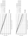
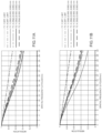
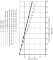
- Figures 8 through 10 plot the polychromatic modulation transfer function (MTF) for points reconstructed on the CDP set at the depth of 3, 1, and 0 diopters, respectively. For each CDP position, two sets of MTFs were plotted, one for fields corresponding to the on-axis MLA and one for fields correspond to the furthest MLA near the edge.
- MTF polychromatic modulation transfer function
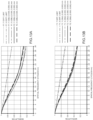
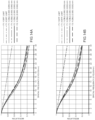
- Figures 11 through 14 plot the polychromatic MTF for reconstructed points shifted away from the CDP by 0.25, 0.5, 0.75, and 1 diopters, respectively. For each depth, two sets of MTFs were plotted, one for fields corresponding to the on-axis MLA and one for fields corresponding to the furthest MLA near the edge.
- Figure 15 plots the polychromatic MTF for the 65°x40° FOV. Across the entire the FOV, the see-through path achieved an average MTF value of over 50% at 30 cycles/degree frequency, corresponding to 20/20 normal vision, and nearly 20% at 60 cycles/degree frequency, corresponding to 20/10 vision or 0.5 arc minute of visual acuity.
Landscapes
- Physics & Mathematics (AREA)
- General Physics & Mathematics (AREA)
- Optics & Photonics (AREA)
- Lenses (AREA)
Description
- The present invention relates generally to the field of head-mounted displays, and more particularly, but not exclusively to head-mounted displays based on integral imaging (InI).
- Head-mounted displays (HMD), also commonly known as near-to-eye displays (NED) or head-worn displays (HWD), have gained significant interest in recent years and stimulated tremendous efforts to push the technology forward for a broad range of consumer applications. For instance, a lightweight optical see-through HMD (OST-HMD), which enables optical superposition of digital information onto a user's direct view of the physical world and maintains see-through vision to the real-world, is one of the key enabling technologies to augmented reality (AR) applications. A wide field-of-view (FOV), immersive HMD, which immerses a user in computer-generated virtual world or a high-resolution video capture of a remote real-world, is a key enabling technology to virtual reality (VR) applications. HMDs find a myriad of applications in gaming, simulation and training, defense, education, and other fields.
- Despite the high promises and the tremendous progress made recently toward the development of both VR and AR displays, minimizing visual discomfort involved in wearing HMDs for an extended period remains an unresolved challenge. One of the key contributing factors to visual discomfort is the vergence-accommodation conflicts (VAC) due to the lack of the ability to render correct focus cues, including accommodation cue and retinal image blur effects. The VAC problem in HMDs stems from the fact that the image source is mostly a 2D flat surface located at a fixed distance from the eye.
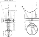
Figure 1 shows a schematic layout of a typical monocular HMD, which mainly includes a 2D microdisplay as the image source and an eyepiece that magnifies the image rendered on the microdisplay and forms a virtual image appearing at a fixed distance from the eye. An OST-HMD requires an optical combiner (e.g. beamsplitter) placed in front of the eye to combine the optical paths of the virtual display and real scene. The conventional HMDs, whether monocular or binocular, see-through or immersive, lack the ability to render correct focus cues for the digital information which may appear at other distances than that corresponding to the virtual image plane. As a result, conventional HMDs fail to stimulate natural eye accommodation response and retinal blurry effects. The problem of lacking correct focus cues in HMDs causes several visual cue conflicts. For instance, a conventional stereoscopic HMD stimulates the perception of 3D space and shapes from a pair of two-dimensional (2D) perspective images, one for each eye, with binocular disparities and other pictorial depth cues of a 3D scene seen from two slightly different viewing positions. Therefore, conventional stereoscopic HMDs force an unnatural decoupling of the accommodation and convergence cues. The cue for the accommodation depth is dictated by the depth of the 2D image plane while the convergence depth of the 3D scene is dictated by the binocular disparities rendered by the image pair. The retinal image blurring cues for virtual objects rendered by the display is mismatched from those created by the natural scene. Many studies have provided strong supportive evidence that these conflicting visual cues related to incorrectly rendered focus cues in conventional HMDs may contribute to various visual artifacts and degraded visual performance. - Several approaches proposed previously may overcome the drawbacks of conventional stereoscopic displays, including volumetric displays, super-multi-view auto-stereoscopic displays, Integral-Imaging-based displays, holographic displays, multi-focal-plane displays, and computational multi-layer displays. Due to their enormous hardware complexity, many of these different display methods are not suitable for implementation in HMD systems. On the other hand, the multi-focal-plane display, integral-imaging, and computational multi-layer approaches are commonly referred to be light field displays and are suitable for head-mounted applications. Their use in HMDs is referred to as head-mounted light field displays.
- Head-mounted light field displays render a true 3D scene by sampling either the projections of the 3D scene at different depths or the directions of the light rays apparently emitted by the 3D scene and viewed from different eye positions. They are capable of rendering correct or nearly correct focus cues and addressing the vergence-accommodation mismatch problem in conventional VR and AR displays. For instance, an integral imaging (InI) based display reconstructs the light fields of a 3D scene by angularly sampling the directions of the light rays apparently emitted by the 3D scene and viewed from different eye positions. As illustrated in
Fig. 2 , a simple InI-based display typically includes a display panel and a 2D array which can be a microlens array (MLA) or pinhole array. The display renders a set of 2D elemental images, each of which represents a different perspective of a 3D scene. The conical ray bundles emitted by the corresponding pixels in the elemental images intersect and integrally create the perception of a 3D scene that appears to emit light and occupy the 3D space. The InI-based display using 2D arrays allows the reconstruction of a 3D shape with full-parallax information in both horizontal and vertical directions, which is its main difference from the conventional auto-stereoscopic displays with only horizontal parallax using one-dimensional parallax barriers or cylindrical lenticular lenses. Since its publication by Lippmann in 1908, the InI-based technique has been widely explored for both capturing the light fields of real scenes and for its use in eyewear-free auto-stereoscopic displays. It has been known for its limitations in low lateral and longitudinal resolutions, narrow depth of field (DOF), and narrow view angle. Compared with all other non-stereoscopic 3D display techniques, the simple optical architecture of an InI technique makes it attractive to integrate with HMD optical system and create a wearable light field display. - However, like other integral-imaging based display and imaging technologies, the current InI-based HMD method suffers from several major limitations: (1) narrow field of view (<30° diagonally); (2) low lateral resolution (about 10 arc minutes in the visual space); (3) low longitudinal resolution (about 0.5 diopters in the visual space); (4) narrow depth of field (DOF) (about 1 diopter for a 10-arc minute resolution criteria); (5) limited eyebox for crosstalk-free viewing(<5mm); and (6) limited resolution of viewing angle (>20 arc minutes per viewing). These limitations not only create significant barriers for adopting the technologies as high-performance solutions, but also potentially undermine the effectiveness of the technology for addressing the accommodation-convergence discrepancy problem.
- Thus, the present disclosure details methods, design and embodiment of a high-performance head-mounted light field display based on integral imaging that overcomes some aspects of the performance limits of the state of the art summarized above.
- In response to the challenges described above, in one of its aspects the present invention provides a high-performance HMD based on integral imaging that offers high lateral and longitudinal resolutions, large depth of field, cross-talk free eyebox, and increased viewing angle resolution. In this regard, the present invention may provide a head-mounted display integral imaging (InI) system, comprising a microscopic InI unit (micro-InI) configured to create light fields of a selected 3D scene at a selected position along an optical axis of the system, and a relay group having a vari-focal element (VFE) disposed therein. The relay group may be disposed on the optical axis at a location so the selected position is an optical conjugate of the relay group, the relay group configured to receive the light fields created by the microscopic InI unit and to create an intermediate 3D scene on the optical axis of the selected 3D scene. The relay group may be configured to tune the position along the optical axis of the intermediate 3D scene. In addition, eyepiece optics may be provided for imaging the intermediate 3D scene from the relay group into an exit pupil of the system for viewing by a user of the head-mounted display system. The microscopic InI unit (micro-InI) may be configured to reproduce full-parallax light fields of a 3D scene having a constrained viewing zone. A see-through unit may also be provided in optical communication with the eyepiece optics to transmit a view of a real world to the eyepiece optics for viewing by a user of the head-mounted display system. The VFE may be disposed at a position optically conjugate to the exit pupil. Further, the field of view of the system may be independent of the optical power of the VFE, and the VFE may be disposed on the optical axis at a location such that the compound optical power of the relay group is maintained constant, independent of the optical power of the VFE. Also, the relay group may be telecentric in object space or may be doubly telecentric. The eyepiece optics may include a wedge-shaped freeform prism. The diagonal field of view of the head-mounted display integral imaging (InI) system may be 35° and may have an optical resolution as high as 2 arc minutes per pixel.
-
WO 2015/184409 A1 describes several hardware configurations and methods for freeform optical display systems.US 2014/0035959 A1 describes high-fidelity light field displays, cameras and two-way displays.WO 2015/134740 A1 describes a wearable 3D augmented reality display, which includes a vari-focal element in the optical path of a micro-Inl display module. - The foregoing summary and the following detailed description of exemplary embodiments of the present invention may be further understood when read in conjunction with the appended drawings, in which:
-
Figure 1 schematically illustrates a conventional, monocular HMD in which an eyepiece magnifies the image rendered on a microdisplay and forms a virtual display appearing at a fixed, far distance from the eye; -
Figure 2 schematically illustrates a near-eye light field display based on integral imaging; -
Figure 3A schematically illustrates an exemplary configuration of a high-performance InI-based head-mounted light field display in accordance with the present invention; -
Figure 3B schematically illustrates an exemplary configuration of a micro-InI unit in accordance with the present invention; -
Figures 4A-4D schematically illustrate an exemplary configuration of a micro-InI unit in accordance with the present invention constructed to provide ray direction control by using: an aperture array (Fig. 4A ), programmable spatial light modulator (Fig. 4B ), a display source with controllable directional emissions engine (Fig. 4C ); and a backlight source with a spatial light modulator as an exemplary controllable directional emissions engine (Fig. 4D ); -
Figure 5 schematically illustrates an exemplary configuration of a relay group in accordance with the present invention with a VFE (vari-focal element) placed at a position conjugate to the exit pupil of the eyepiece; -
Figures 6A-6D schematically illustrate an exemplary configuration of an optical see-through InI-HMD design in accordance with the present invention using a freeform waveguide prism where part of the vari-focal relay group is incorporated into the eyepiece, withFig. 6A showing the display path layout,Fig. 6B showing the see-through view layout,Fig. 6C showing a segmented rear surface of the waveguide prism for extended see-through view, andFig. 6D showing a front view of the rear surface of the waveguide prism; -
Figures 7A ,7B schematically illustrate an exemplary configuration of 2D optical layout of an InI-HMD design configuration in accordance with the present invention, withFig. 7A showing the light field display path andFig. 7B the see-through path; -
Figures 8A, 8B illustrate MTF (modulation transfer function) plots for the reconstruction central depth plane (CDP) depth of 3 diopters for fields on-axis (Fig. 8A ) and for fields for the furthest MLA (micro lens array) element near the edge of the MLA (Fig. 8B ); -
Figures 9A, 9B illustrate MTF plots for the reconstruction CDP depth of 2 diopters for fields on-axis to the MLA (Fig. 9A ) and fields for the furthest MLA element near the edge of the MLA (Fig. 9B ); -
Figures 10A, 10B illustrate MTF plots for the reconstruction CDP depth of 0 diopters for fields on-axis to the MLA (Fig. 10A ) and for fields for the furthest MLA element near the edge of the MLA (Fig. 10B ); -
Figures 11A, 11B illustrate MTF plots for the reconstruction points shifted away from CDP by 0.25 diopters for fields on-axis to the MLA (Fig. 11A ) and for fields for the furthest MLA element near the edge of the MLA (Fig. 11B ); -
Figures 12A, 12B illustrate MTF plots for the reconstruction points shifted away from CDP by 0.5 diopters for fields on-axis to the MLA (Fig. 12A ) and for fields for the furthest MLA element near the edge of the MLA (Fig. 12B ); -
Figures 13A, 13B illustrate MTF plots for the reconstruction points shifted away from CDP by 0.75 diopters for fields on-axis to the MLA (Fig. 13A ) and for fields for the furthest MLA element near the edge of the MLA (Fig. 13B ); -
Figures 14A, 14B illustrate MTF plots for the reconstruction points shifted away from CDP by 1 diopter for fields on-axis to the MLA (Fig. 14A ) and for fields for the furthest MLA element near the edge of the MLA (Fig. 14B ); and -
Figure 15 illustrates the MTF for the see-through path FOV 65°x40°. - Referring now to the figures, wherein like elements are numbered alike throughout, as shown in
Fig. 3A , aHMD system 100 in accordance with the present invention may include three key subsystems: I) a microscopic InI unit (micro-Inl) 130, II) arelay group 120 with a vari-focal element (VFE) 122 disposed therein for receiving the light fields from theInI unit 130, and III)eyepiece optics 110 for receiving the tuned intermediate 3D scene from therelay group 120. As illustrated inFig. 3B , themicro-InI unit 130 can reproduce the full-parallax light fields of a 3D scene seen from a constrained viewing zone, where the full-parallax light fields offer the change of view perspectives of a 3D scene from both horizontal and vertical viewing directions. The constrained viewing zone optically corresponds to limiting the aperture of themicro-InI unit 130, and the constrained viewing zone is optically conjugate to the exit pupil of thedisplay system 100 where a viewer's eye is placed to view the reconstructed 3D scene. Therelay group 120 creates an intermediate image of the 3D scene reconstructed by themicro-InI unit 130 with a tunable position of its central depth plane (CDP). Depending on the magnification power of theeyepiece 110, the position of the CDP may be tunable in the range from about 0.5mm to as large as hundreds of millimeters to create the perception of a 3D scene with a large depth range spanning from the optical infinity (0 diopter) to as close as 20cm (5 diopters). Therelay group 120 may also facilitate the flip of the concavity of the reconstructed 3D scene AOB. Theeyepiece optics 110 reimages the tunable 3D light fields into a viewer's eye and enlarges the tunable depth range of the 3D light fields into a large depth volume spacing from meters far to as close as a few centimeters. A see-through unit (not shown), which may be optics with a beamsplitter function, may optically communicate with theeyepiece optics 110 to optically enable non-obtrusive view of a real-world scene if a see-through view is desired. Themicro-InI unit 130 ofFig. 3A , as further illustrated inFig. 3B , may include a high-resolution microdisplay and a micro-lens array (MI,A) 132. The focal length of thelenslets 133 in theMLA 132 is denoted as fMLA and the gap between themicrodisplay 134 and theMLA 132 is noted as g. A set of 2D elemental images, each representing a different perspective of a 3D scene AOB, may be displayed on the high-resolution microdisplay 134. Through theMLA 132, each elemental image works as a spatially-incoherent object and the conical ray bundles emitted by the pixels in the elemental images intersect and integrally create the perception of a 3D scene that appears to emit light and occupy the 3D space. The central depth plane (CDP) of the reconstructed miniature scene, with a depth range of z0, is located by the distance lcdp measured from theMLA 132. Such anInI system 130 allows the reconstruction of a 3D surface shape AOB with parallax information in both horizontal and vertical directions. The light field of the reconstructed 3D scene (i.e., the curve AOB inFig. 3B ) may be optically coupled intoeyepiece optics 110 via therelay group 120 for viewing by a user. In a resolution priority InI system (fMLA ≠ g), the central depth plane CDP of the reconstructed 3D scene is optically conjugate to themicrodisplay 134 and its location is given by
micro-InI unit 130, which may be expressed by
- As shown in
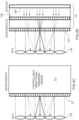
Figs. 3A ,4A , optionally, anaperture array 136, including a group of ray-limiting apertures that matches the pitch of theMLA 132, may be inserted between themicrodisplay 134 andMLA 132. The small aperture corresponding to eachmicrolens 133 allows rays within the designed viewing window to propagate through the optics and reach the eyebox while blocking unwanted rays from reaching anadjacent microlens 133 or while blocking rays from neighboring elemental images to reach amicrolens 133. For instance, the black zone between the aperture A1 and A2 blocks the dashed rays originated from point P1 from reaching the MLA2 adjacent to the lenslet MLA1. These blocked rays are typically the main source of view cross-talk and ghost images observed in an InI display system. The distance from themicrodisplay 134 to theaperture array 136 is denoted as ga and the diameter of aperture opening is denoted as pa, which may be constrained by

MLA 132. - One drawback in using an
aperture array 136 with a fixed aperture size is that it can partially block rays for pixels located near the edge of each elemental images if the size of the elemental image changes. As illustrated inFigure 4A , a small part of the rays from point P1 which are supposed to propagate through lenslet MLA1 are blocked by the black zone between aperture A1 and aperture A2, causing vignetting-like effects such that viewer may observe reduction of image brightness for points near the edge of each elemental images.Figure 4B shows an alternative configuration to that ofFig. 4A in which theaperture array 136 is replaced by a programmable spatial light modulator (SLM) 135 so that the size and shape of each aperture can be dynamically adapted to avoid partially blocking desired rays.Figure 4C shows another embodiment of a micro-InI unit in accordance with the present invention in which themicrodisplay 134 andaperture array 136 are replaced by adisplay source 131 with controllable directional emissions, where the light emission direction can be controlled precisely so that the rays from each pixel will only reach theircorresponding MLA lenslet 133.Figure 4D demonstrates one possible configuration ofsuch display source 131 where a spatiallight modulator 135 is inserted between abacklight source 138 with non-direction emission and non-self-emissive microdisplay 137. The spatiallight modulator 135 may be set to program and control the cone angle of the rays that illuminate themicrodisplay 137 and reach theMLA 132. - A conventional InI-based display system can typically suffer from a limited depth of field (DOF) due to the rapid degradation of spatial resolution as the depths of 3D reconstruction points shift away from that of the CDP. For instance, the 3D scene volume may need to be limited to less than 0.5 diopters in order to maintain a spatial resolution of 3 arc minutes or better in the visual space. In order to render a much larger 3D scene volume while maintaining a high spatial resolution, such as in the exemplary configuration of
Fig. 3A , arelay group 120 with an electronically-controlled vari-focal element 122 sandwiched inside is inserted between the micro-InI 130 and theeyepiece 110. Exemplary VFE's 122 include liquid lenses, liquid crystal lenses, deformable mirrors, or any other tunable optical technology, such as electrically tunable optical technology. By dynamically controlling the optical power, ϕR, of therelay group 120 by applying different voltages to theVFE 122, therelay group 120 forms an intermediate image A'O'B' of the reconstructed miniature 3D scene created by themicro-Inl 130. The central depth position CDP of the relayed intermediate scene is tunable axially (along the optical axis) with respect to theeyepiece 110. As a result, the depth volume of the magnified 3D virtual scene by theeyepiece 110 can be shifted axially from very close (e.g. 5 diopters) to very far (e.g. 0 diopter) while maintaining high lateral and longitudinal resolutions. -
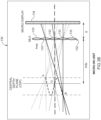
Figure 5 schematically illustrates an exemplary configuration of the vari-focal relay group 120, such as therelay group 120 ofFig. 3A , including a front lens group "Front Relay" 126 adjacent to themicro-InI unit 130,VFE optics 122 located in the middle functioning as the system stop, and rear lens group "Rear Relay" 124 adjacent to theeyepiece 110. The compound power, ϕR, of therelay group 120 is given by
front lens group 126,VFE 122, and therear lens group 124, respectively. t1 and t2 are the spaces between thefront lens group 126 andVFE 122 and between theVFE 122 and therear lens group 124. z0 is the axial distance between the front lens group and the 3D scene reconstructed by themicro-InI unit 130. The axial position of the relayed intermediate scene is given by
- The lateral magnification of the vari-focal relay system is given by

- Assuming ϕe is the optical power of the
eyepiece 110 and ZRCDP is the distance from the relayed CDP to theeyepiece 110, the apparent CDP position of the reconstructed 3D virtual scene through theeyepiece 110 is given by
- The lateral magnification of the entire system through the
eyepiece 110 is given by
- The field of view (FOV) of the entire system through the
eyepiece 110 is given by, FOV =
eyepiece 110 andrear relay lens 124; z xp is the spacing between the exit pupil and theeyepiece 110; h0 is the image height of the reconstructed scene, and we further define uvfe = [(1- zxpϕe) - (z xp + (1 - z xpϕe)t3)ϕ2] , and hvfe = [(1 - z xpϕe) - (z xp + (1 - z xpϕe)t3)ϕ2] - [(z xp + (1 - z xpϕe)t3)ϕ2 + ((1 - z xpϕe) - (z xp + (1 - z xpϕe)t3)ϕ2)]t2. - When the
VFE 122 is set to be an optical conjugate to the exit pupil of the eyepiece 110 ((i.e. hvfe=0) where the entrance pupil of the eye is placed to view thedisplay 134, we have hvfe=0 and the FOV is independent of the optical power of theVFE 122. The equation in Eq. (9) is simplified into:
- As illustrated in
Fig. 5 , a preferred embodiment of the vari-focal relay group 120 is the placement of theVFE 122 at the back focal length of the front relay group 26 (i.e. t1=1/ϕ1) to make theVFE 122 an optical conjugate to the exit pupil of the eyepiece 110 ((i.e. hvfe=0). With this preferred embodiment, the compound power, ϕR, of therelay group 120 given by Eq. (4) is simplified into:
- The lateral magnification of the vari-focal relay system given by Eq. (6) is simplified into

- And so does the lateral magnification of the entire system given by Eq. (8).
- When t1=1/ϕ1 and hvfe=0, the FOV of the system is further simplified into

- As demonstrated by Eqs. (10) through (13), the careful position of the
VFE 122 in the preferred manner ensures that the compound optical power of therelay group 120 is maintained constant, independent of the optical power of theVFE 122 due to constant chief ray directions owing to the property of object-space telecentricity. As further demonstrated by Eq. (13), the subtended field angle of the display through theeyepiece 110 is further maintained constant, independent of the optical power of theVFE 122. Maintaining a constant optical power for therelay group 120 helps the virtually reconstructed 3D scene achieve constant field of view regardless of the focal depths of the CDP. Therefore a much larger volume of a 3D scene could be visually perceived without seams or artifacts in a gaze-contingent or time-multiplexing mode. It is worth noting that the lateral magnification of therelay group 120 given by Eq. (12) can be further maintained constant if t2=1/ϕ2 is satisfied, which makes the vari-focal relay group 120 a double-telecentric system. - The
eyepiece 110 inFig. 3A can take many different forms. For instance, to achieve a compact optical design of an optical see-through HMD, a wedge-shaped freeform prism can be adopted, through which the 3D scene reconstructed by themicro-InI unit 130 andrelay group 120 is magnified and viewed. To enable see-through capability for AR systems, a freeform corrector lens with one of the surfaces coated with beamsplitter coating can be attached to the freeform prism eyepiece to correct the viewing axis deviation and undesirable aberrations introduced by the freeform prism to the real-world scene. - In another aspect of the present invention, part of the
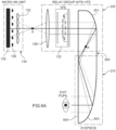
relay group 120 may be incorporated into theeyepiece optics 110, such as freeform eyepiece, such that the tunable intermediate 3D scene is formed inside the freeform eyepiece. In such a context, the eyepiece may be a wedge-shaped freeform waveguide prism, for example.Figure 6A schematically illustrates the concept of a freeform waveguide-like prism 850 formed by multiple freeform optical surfaces. The exit pupil is located where the use's eye is placed to view the magnified 3D scene. In the design, part of atraditional relay group 220 following theVFE 122 is incorporated into theprism 850 and fulfilled by thetop portion 851 of thefreeform waveguide prism 850 contained within the box labeled "Relay Group with VFE." A light ray emitted from a 3D point (e.g. A) is first refracted by a closestoptical element 126 of therelay group 220 and transmitted into theprism 850, followed by a reflection by one or multiple freeform surfaces to create an intermediate image (e.g. A'). The axial position of the intermediate image (e.g. A') is tunable by theVFE 122. Multiple consecutive reflections by the subsequent surfaces and a final refraction through the exit surface 855allow the ray reaching the exit pupil of the system. Multiple bundles of rays from different elemental images may exist, but do so apparently from the same object point, each of which bundles represents a different view of the object, impinging on different locations of the exit pupil. These ray bundles integrally reconstruct a virtual 3D point (e.g. "A") located in front of the eye. Rather than requiring multiple optical elements, the optical path is naturally folded within amulti-surface prism 850, which helps reduce the overall volume and weight of the optics substantially when compared with designs using rotationally symmetric elements. Compared with a design using a traditional wedge-shaped 3-surface prism, the waveguide-like eyepiece design incorporates part of the relay function, enabling a much more compact system than combining astandalone relay group 120 with a 3-surface prism. Besides the advantage of compactness, the waveguide-like multi-fold eyepiece design offers a much more favorable form factor, because it enables the ability to fold the remaining relay group and micro-InI unit horizontally to the temple sides. The multiple folding not only yields a much more weight-balanced system, but also enables a substantially larger see-through FOV than using a wedge-shaped prism. - To enable see-through capability for AR systems, the
bottom part 853 of the rear surface, marked as the eyepiece portion, of theprism 850 inFig. 6A can be coated as a beamsplitting mirror, and afreeform corrector lens 840 including at least two freeform optical surfaces, may be attached to the rear surface of theprism 850 to correct the viewing axis deviation and undesirable aberrations introduced by thefreeform prism 850 to the real-world scene. The see-through schematic layout is shown inFig. 6B . The rays from the virtual light field are reflected by the rear surface of theprism 850 while the rays from a real-world scene are transmitted through thefreeform corrector lens 840 andprism 850. The front surface of thefreeform corrector lens 840 matches the shape of the rear surface of theprism 850. The back surface of thefreeform corrector lens 840 may be optimized to minimize the shift and distortion introduced to the rays from a real-world scene when the lens is combined with theprism 850. The additional corrector lens "compensator" does not noticeably increase the footprint and weight of the overall system. - In another aspect of the present invention, the
bottom part 853 of the rear surface, marked as the eyepiece portion, of theprism 850 inFig. 6A may be divided into two segments, the segment 853-1 and the segment 853-2. As schematically illustrated inFig. 6C , the segment of 853-1 may be a reflective or partial reflective surface which receives the light fields generated by the micro-InI unit. A beamsplitting mirror coating on the segment of 853-1 also allows the transmission of the light rays from a real-world scene. The segment 853-2 is a transmissive or semi-transmissive surface which only receives the light rays from a real-world scene, while it does not receive the light fields generated by themicro-InI unit 130.Fig. 6D schematically illustrates a front view of the rear surface of theprism 850. The two surface segments, 853-1 and 853-2, intersect at an upper boundary of the aperture window required to receive the reconstructed 3D light fields by themicro-InI unit 130, and they may be made by two separate freeform surfaces. The division of the bottom part of therear surface 853 into two separate segments 853-1, 853-2 with different light paths provides the ability to substantially enlarge the FOV of the see-through view beyond the FOV of the display path without being subject to the constraints of the virtual display path. As shown inFig. 6C , afreeform corrector lens 840 may be attached to the rear surface of theprism 850 to correct the viewing axis deviation and undesirable aberrations introduced by thefreeform prism 850 to the real-world scene. The rays from the virtual light field are reflected by the segment 853-1 of the rear surface of theprism 850 while the rays from a real-world scene are transmitted through both the segments 853-1 and 853-2 of theprism 850 and thefreeform corrector lens 840. The surface segment 853-2 may be optimized to minimize visual artifacts of see-through view when it is combined with thefreeform corrector lens 840. The front surface of thefreeform corrector lens 840 matches the shape of the surface segments 853-1 and 853-2 of theprism 850. The back surface of thefreeform corrector lens 840 may be optimized to minimize the shift and distortion introduced to the rays from a real-world scene when thefreeform corrector lens 840 is combined with theprism 850. - In accordance with yet another aspect of the present invention,
Figure 7A schematically illustrates an optical design of a physical system that embodies the conceptual system ofFig. 6A .Figure 7A illustrates the 2D optical layout of the light field display path, andFig. 7B shows the optical layout of the see-through path. The optical system of the light field display includes a micro-InI unit, a relay group with VFE, and a freeform waveguide. A part of the relay group may be incorporated into the waveguide. The Micro-InI unit may include a microdisplay S0, a pinhole array S1, and a microlens array S2. The relay group may include four lenses, a commercially available VFE (Electrical Lens EL 10-30 by Optotune Inc.), and two freeform surfaces (Surface S19 and S20). Thefreeform waveguide prism 900 may be formed by multiple freeform optical surfaces which are labeled as S19, S20, S21, and S22, respectively. In the design, part of a traditional relay group following the VFE may be incorporated into theprism 900 and fulfilled by the Surface S19 and S20. A light ray emitted from a 3D point (e.g. A) is first refracted by the surface S19 of theprism 900, followed by a reflection by the surface S20 to create an intermediate image (e.g. A'). The axial position of the intermediate image (e.g. A') is tunable by the VFE. Two more consecutive reflections by the surfaces S21' and S22-1 and a final refraction through the surface S21 allow the ray to reach the exit pupil of the system. There exist multiple bundles of rays from different elemental images but apparently from the same object point, each of which represents a different view of the object, impinging on different locations of the exit pupil. These ray bundles integrally reconstruct a virtual 3D point located in front of the eye. The rays reflected by the Surface S21' of the waveguide are required to satisfy the condition of total internal reflection. The rear surfaces S22-1, S22-2 of theprism 900 may be coated with a mirror coating for building an immersive HMD system which blocks the view of the real-world scene. Alternatively, the surface S22-1 may be coated with a beamsplitting coating if optical see-through capability is desired using the auxiliary lens, as shown inFig. 7B . - It should be noted that in the design disclosed hereby the Z-axis is along the viewing direction, the Y-axis is parallel to the horizontal direction aligning with interpupilary direction, and the X-axis is in the vertical direction aligning with the head orientation. As a result, the overall waveguide system is symmetric about the horizontal (YOZ) plane, and the optical surfaces (S19, S20, S21, and S22) are decentered along the horizontal Y-axis and rotated about the vertical X-axis. The optical path is folded in the horizontal YOZ plane. This arrangement allows the micro-InI unit and the vari-focal relay group to be mounted on the temple side of the user's head, resulting in a balanced and ergonomic system packaging.
- Table 1 highlighted some of the key performance specifications for the system of
Fig. 7A . The system offers the ability to render the true 3D light field of a 3D scene which subtends a diagonal FOV of 35° and achieves an optical resolution as high as 2 arc minutes per pixel in the visual space. Furthermore, the system offers a large depth range, tunable from 0 to 5 diopters, with a high longitudinal resolution of about 0.1 diopters for a monocular display. Moreover, the system achieves a high view density of about 0.5/mm2, where the view density, σ, is defined as the number of unique views per unit area on the exit pupil, given by:
Table 1-First-order system specifications Tunable depth range of central depth plane (CDP) 0 ~ 5 diopters Field of view (Virtual Display) 35° (diagonal), or 30.5° (Horizontal) x 17.5° (Vertical) at CDP Field of view (See-through) >75° (diagonal), or >65° (Horizontal) x 40° (Vertical) Focal length of front relay group 24 mm Focal length of rear relay group 24 mm Focal range of the tunable lens 75-100mm (8.5 diopters) Eyepiece focal length, feye 27.5 mm Exit pupil diameter 6 mm Pitch of the lenslet in MLA 1 mm F-number of the MLA 3.3 - An exemplary implementation of the system of
Fig. 7A is provided, Tables 2 through 5, in form of the optical surface data. Table 2 summarizes the basic parameters of the display path (units: mm). Tables 3 through 5 provide the optimized coefficients defining the non-spherical optical surfaces.Table 2-Optical specifications of the InI-HMD display path Element number or name Surfac e No. Surface Type Y Radius Thicknes s Material Refract Mode Aperture Sphere Infinity 2.215 Refract MLA S1 Asphere -5.32 3 PMMA Refract S2 Asphere -1.48 13.833 Refract S3 Sphere Infinity 10.547 Refract Front relay group S4 Sphere 35.09 6.6 NBK7_SCHOTT Refract S5 Sphere -35.09 9.970 Refract S6 Sphere 12.92 4.3 NBK7_SCHOTT Refract S7 Sphere Infinity 2.457 Refract S8 Sphere -39.78 2.5 NSF11_SCHOT T Refract S9 Sphere 39.78 1.75 Refract VFE S10 Sphere Infinity 1.15 Refract S11 Sphere Infinity 0.5 BK7_SCHOTT Refract S12 Sphere Infinity 2.758 'OL1024' Refract S13 Sphere -28.5714 4.492 Refract S14 Sphere Infinity 0.5 BK7_SCHOTT Refract S15 Sphere Infinity 1.15 Refract S16 Sphere Infinity 1 Refract Lens S17 Sphere 40.67 5.3 NBK7_SCHOTT Refract S18 Sphere -40.67 0 Refract Waveguid e S19 XY Polynomia 1 31.0416 7 0 PMMA Refract S20 XY Polynomia l -54.2094 0 PMMA Reflect S21 XY Polynomia l -145.276 0 PMMA Reflect S22 XY Polynomia l -47.3572 0 PMMA Reflect S21' XY Polynomia l -145.276 0 Refract - A high resolution microdisplay with pixels as small as 6µm is adopted to achieve a high resolution virtual reconstructed 3D image. To achieve such high-resolution imaging for the micro-InI unit, a microlens array (MI,A) formed by aspherical surfaces may specifically be designed. Each of the aspherical surfaces of the MLA may be described as,

Table 3-Aspherical surface definitions for microlens array (MLA) S1 S2 Y Radius -5.32 -1.48 Conic Constant (K) 30 -0.809 4th Order Coefficient (A) -0.157 -0.013 6th Order Coefficient (B) -0.092 0.002 - To enable enlarged see-through FOV, the
freeform waveguide prism 900 may be formed by five freeform surfaces, labeled as surface S19, S20, S21/S21', S22-1, and S22-2, respectively. The freeform corrector lens may be formed by two freeform surfaces, in which the front surface shares the same surface specifications as the surfaces S22-1 and S22-2 of thewaveguide prism 900 and the rear surface is denoted as surface S23. The surface segment of S22-1 is a reflective or partial reflective surface which receives the light fields generated by the micro-InI unit. A beamsplitting mirror coating on the segment of S22-1 also allows the transmission of the light rays from a real-world scene for see-through capability. The surface segment S22-2 is a transmissive or semi-transmissive surface which only receives the light rays from a real-world scene, while it does not receive the light fields generated by the micro-InI unit. - The freeform surfaces, including S19, S20, S21/S21', S22-1, and S23 may be described mathematically as

- During the design process, the specifications for the Surface segment S22-1 were obtained after the optimization of the light field display path through the
prism 900 composed of the micro-InI unit, the relay lens group, and the surfaces S19. S20, S21/21', and S22-1. The required aperture dimensions of Surfaces S20 and S22-1 were determined first for the light field display path. Then Surfaces S20, S21 and S22-1 were imported into 3D modeling software such as Solidworks® from which the Surface S22-2 was created. The shape of the Surface S22-2 was created in the modeling software by satisfying the following requirements: (1) it intersects with Surface S22-1 along or above the upper boundary line of the required aperture for surface S22-1 defined by the display path; (2) along the intersection line between the surface S22-2 and S22-2, the surface slopes at the intersection points on the surface S22-2 approximately match, if not equal, with those corresponding points on the surface S22-1 to ensure the two surfaces to appear to be nearly continuous, which minimizes visual artifacts to the see-through view when it is combined with a matching freeform corrector lens; (3) the Surface S22-2 intersects with the surface S20 along or below the lower boundary line of the required aperture for surface S20, defined by the display path; and (4) the overall thickness between the surface S21 and S22-2 is minimized. Finally, a freeform shape of the Surface S22-2 is obtained in the 3D modeling software which is combined with the surfaces S19, S20, S21/21', and S22-1 to create an enclosed freeform waveguide prism.Fig. 7B demonstrated a substantially enlarged see-through FOV through the method described above.Table 4-Surface definition for freeform surface S19 Y Radius 31.0417 Y Curvature 3.2215e-2 Conic Constant (SCO K | C1) -30 X (SCO X | C2) 0 Y (SCO Y | C3) 0 X**2 (SCO X2 | C4) -0.0181749 X * Y (SCO XY | C5) 0 Y**2 (SCO Y2 | C6) -0.03201 X**3 (SCO Y3 | C7) 0 X**2 * Y (SCO X2Y | C8) -0.002337 X Y**2 (SCO XY2 | C9) 0 Y**3 (SCO Y3 | C10) -0.00340584 X**4 (SCO X4 | C11) 2.214179429e-005 X**3 * Y (SCO X3Y | C12) 0 X**2 * Y**2 (SCO X2Y2 | C13) -8.34173481e-005 X * Y**3 (SCO XY3 | C14) 0 Y**4 (SCO Y4 | C15) -0.00012019 X**5 (SCO X5 | C16) 0 X**4 * Y (SCO X4Y | C17) -1.9551358e-006 X**3 * Y**2 (SCO X3Y2 | C18) 0 X**2 * Y**3 (SCO X2Y3 | C19) -5.7523828e-007 X * Y**4 (SCO XY4 | C20) 0 Y**5 (SCO Y5 | C21) -2.18978576e-006 X**6 (SCO X6 | C22) -1.08276112e-007 X**5 * Y (SCO X5Y | C23) 0 X**4 * Y**2 (SCO X4Y2 | C24) -3.584137e-007 X**3 * Y**3 (SCO X3Y3 | C25) 0 X**2 * Y**4 (SCO X2Y4 | C26) 9.1214167e-008 X * Y**5 (SCO XY5 | C27) 0 Y**6 (SCO Y6 | C28) -5.28011679e-009 X**7 (SCO X7 | C29) 0 X**6 * Y (SCO X6Y | C30) 0 X**5 * Y**2 (SCO X5Y2 | C31) 0 X**4 * Y**3 (SCO X4Y3 | C32) 0 X**3 * Y**4 (SCO X3Y4 | C33) 0 X**2 * Y**5 (SCO S2Y5 | C34) 0 X * Y**6 (SCO XY6 | C35) 0 Y**7 (SCO Y7 | C36) 0 X**8 (SCO X8 | C37) 0 X**7 * Y (SCO X7Y | C38) 0 X**6 * Y**2 (SCO X6Y2 | C39) 0 X**5 * Y**3 (SCO X5Y3 | C40) 0 X**4 * Y**4 (SCO X4Y4 | C41) 0 X**3 * Y**5 (SCO X3Y5 | C42) 0 X**2 * Y**6 (SCO X2Y6 | C43) 0 X * Y**7 (SCO XY7 | C44) 0 Y**8 (SCO Y8 | C45) 0 X**9 (SCO X9 | C46) 0 X**8 * Y (SCO X8Y | C47) 0 X**7 * Y**2 (SCO X7Y2 | C48) 0 X**6 * Y**3 (SCO X6Y3 | C49) 0 X**5 * Y**4 (SCO X5Y4 | C50) 0 X**4 * Y**5 (SCO X4Y5 | C51) 0 X**3 * Y**6 (SCO X3Y6 | C52) 0 X**2 * Y**7 (SCO X2Y7 | C53) 0 X * Y**8 (SCO XY8 | C54) 0 Y**9 (SCO Y9 | C55) 0 X**10 (SCO X10 | C56) 0 X**9 * Y (SCO X9Y | C57) 0 X**8 * Y**2 (SCO X8Y2 | C58) 0 X**7 * Y**3 (SCO X7Y3 | C59) 0 X**6 * Y**4 (SCO X6Y4 | C60) 0 X**5 * Y**5 (SCO X5Y5 | C61) 0 X**4 * Y**6 (SCO X4Y6 | C62) 0 X**3 * Y**7 (SCO X3Y7 | C63) 0 X**2 * Y**8 (SCO X2Y8 | C64) 0 X * Y**9 (SCO XY9 | C65) 0 Y**10 (SCO Y10 | C66) 0 Table 5-Surface definition for freeform surface S20 Y Radius -54.2094 Y Curvature -1.845e-2 Conic Constant (SCO K | C1) -13.0997 X (SCO X | C2) 0 Y (SCO Y | C3) 0 X**2 (SCO X2| C4) 0.0011699 X * Y (SCO XY | C5) 0 Y**2 (SCO Y2 | C6) 0.00676927 X**3 (SCO Y3 | C7) 0 X**2 * Y (SCO X2Y | C8) -4.52710486e-005 X Y**2 (SCO XY2 | C9) 0 Y**3 (SCO Y3 | C10) -0.00011081 X**4 (SCO X4| C11) -1.1510996e-005 X**3 * Y (SCO X3Y | C12) 0 X**2 * Y**2 (SCO X2Y2 | C13) -9.13752747e-006 X * Y**3 (SCO XY3 | C14) 0 Y**4 (SCO Y4 | C15) -5.5289301e-006 X**5 (SCO X5 | C16) 0 X**4 * Y (SCO X4Y | C17) -8.8179807e-007 X**3 * Y**2 (SCO X3Y2 | C18) 0 X**2 * Y**3 (SCO X2Y3 | C19) -1.06187669e-006 X * Y**4 (SCO XY4 | C20) 0 Y**5 (SCO Y5 | C21) -3.38263553e-007 X**6 (SCO X6 | C22) 4.77710263e-008 X**5 * Y (SCO X5Y | C23) 0 X**4 * Y**2 (SCO X4Y2 | C24) 6.21915481e-008 X**3 * Y**3 (SCO X3Y3 | C25) 0 X**2 * Y**4 (SCO X2Y4 | C26) 1.43552488e-007 X * Y**5 (SCO XY5 | C27) 0 Y**6 (SCO Y6 | C28) 5.362211474e-008 X**7 (SCO X7 | C29) 0 X**6 * Y (SCO X6Y | C30) 1.193262499e-008 X**5 * Y**2 (SCO X5Y2 | C31) 0 X**4 * Y**3 (SCO X4Y3 | C32) -6.01716948e-009 X**3 * Y**4 (SCO X3Y4 | C33) 0 X**2 * Y**5 (SCO S2Y5 | C34) -8.19603928e-009 X * Y**6 (SCO XY6 | C35) 0 Y**7 (SCO Y7 | C36) -2.505270966e-009 X**8 (SCO X8 | C37) -8.149026e-010 X**7 * Y (SCO X7Y | C38) 0 X**6 * Y**2 (SCO X6Y2 | C39) -1.84757517e-010 X**5 * Y**3 (SCO X5Y3 | C40) 0 X**4 * Y**4 (SCO X4Y4 | C41) 2.388128888e-010 X**3 * Y**5 (SCO X3Y5 | C42) 0 X**2 * Y**6 (SCO X2Y6 | C43) 1.61835037e-010 X * Y**7 (SCO XY7 | C44) 0 Y**8 (SCO Y8 | C45) 3.966177607e-011 X**9 (SCO X9 | C46) 0 X**8 * Y (SCO X8Y | C47) 0 X**7 * Y**2 (SCO X7Y2 | C48) 0 X**6 * Y**3 (SCO X6Y3 | C49) 0 X**5 * Y**4 (SCO X5Y4 | C50) 0 X**4 * Y**5 (SCO X4Y5 | C51) 0 X**3 * Y**6 (SCO X3Y6 | C52) 0 X**2 * Y**7 (SCO X2Y7 | C53) 0 X * Y**8 (SCO XY8 | C54) 0 Y**9 (SCO Y9 | C55) 0 X**10 (SCO X10 | C56) ' 0 X**9 * Y (SCO X9Y | C57) 0 X**8 * Y**2 (SCO X8Y2 | C58) 0 X**7 * Y**3 (SCO X7Y3 | C59) 0 X**6 * Y**4 (SCO X6Y4 | C60) 0 X**5 * Y**5 (SCO X5Y5 | C61) 0 X**4 * Y**6 (SCO X4Y6 | C62) 0 X**3 * Y**7 (SCO X3Y7 | C63) 0 X**2 * Y**8 (SCO X2Y8 | C64) 0 X * Y**9 (SCO XY9 | C65) 0 Y**10 (SCO Y10 | C66) 0 Table 6-Surface definition for freeform surface S21/S21' Y Radius -145.276 Y Curvature -6.88e-3 Conic Constant (SCO K | C1) -1.5654 X (SCO X | C2) 0 Y (SCO Y | C3) 0 X**2 (SCO X2 | C4) -0.0142277 X * Y (SCO XY | C5) 0 Y**2 (SCO Y2 | C6) 0.00392684 X**3 (SCO Y3 | C7) 0 X**2 * Y (SCO X2Y | C8) 0.000646111 X Y**2 (SCO XY2 | C9) 0 Y**3 (SCO Y3 | C10) 2.44041e-005 X**4 (SCO X4 | C11) 0.000151 X**3 * Y (SCO X3Y | C12) 0 X**2 * Y**2 (SCO X2Y2 | C13) -8.2192e-006 X* Y**3 (SCO XY3 | C14) 0 Y**4 (SCO Y4 | C15) -3.028061e-007 X**5 (SCO X5 | C16) 0 X**4 * Y (SCO X4Y | C17) -4.13244e-006 X**3 * Y**2 (SCO X3Y2 | C18) 0 X**2 * Y**3 (SCO X2Y3 | C19) 2.964542e-008 X * Y**4 (SCO XY4 | C20) 0 Y**5 (SCO Y5 | C21) 1.127521e-009 X**6 (SCO X6 | C22) 4.4371187e-008 X**5 * Y (SCO X5Y | C23) 0 X**4 * Y**2 (SCO X4Y2 | C24) 2.7676459e-008 X**3 * Y**3 (SCO X3Y3 | C25) 0 X**2 * Y**4 (SCO X2Y4 | C26) -3.277381e-011 X * Y**5 (SCO XY5 | C27) 0 Y**6 (SCO Y6 | C28) -1.4480674e-012 X**7 (SCO X7 | C29) 0 X**6 * Y (SCO X6Y | C30) 0 X**5 * Y**2 (SCO X5Y2 | C31) 0 X**4 * Y**3 (SCO X4Y3 | C32) 0 X**3 * Y**4 (SCO X3Y4 | C33) 0 X**2 * Y**5 (SCO S2Y5 | C34) 0 X * Y**6 (SCO XY6 | C35) 0 Y**7 (SCO Y7 | C36) 0 X**8 (SCO X8 | C37) 0 X**7 * Y (SCO X7Y | C38) 0 X**6 * Y**2 (SCO X6Y2 | C39) 0 X**5 * Y**3 (SCO X5Y3 | C40) 0 X**4 * Y**4 (SCO X4Y4 | C41) 0 X**3 * Y**5 (SCO X3Y5 | C42) 0 X**2 * Y**6 (SCO X2Y6 | C43) 0 X * Y**7 (SCO XY7 | C44) 0 Y**8 (SCO Y8 | C45) 0 X**9 (SCO X9 | C46) 0 X**8 * Y (SCO X8Y | C47) 0 X**7 * Y**2 (SCO X7Y2 | C48) 0 X**6 * Y**3 (SCO X6Y3 | C49) 0 X**5 * Y**4 (SCO X5Y4 | C50) 0 X**4 * Y**5 (SCO X4Y5 | C51) 0 X**3 * Y**6 (SCO X3Y6 | C52) 0 X**2 * Y**7 (SCO X2Y7 | C53) 0 X * Y**8 (SCO XY8 | C54) 0 Y**9 (SCO Y9 | C55) 0 X**10 (SCO X10 | C56) 0 X**9 * Y (SCO X9Y | C57) 0 X**8 * Y**2 (SCO X8Y2 | C58) 0 X**7 * Y**3 (SCO X7Y3 | C59) 0 X**6 * Y**4 (SCO X6Y4 | C60) 0 X**5 * Y**5 (SCO X5Y5 | C61) 0 X**4 * Y**6 (SCO X4Y6 | C62) 0 X**3 * Y**7 (SCO X3Y7 | C63) 0 X**2 * Y**8 (SCO X2Y8 | C64) 0 X * Y**9 (SCO XY9 | C65) 0 Y**10 (SCO Y10 | C66) 0 Table 7-Surface definition for freeform surface S22-1 Y Radius -47.3572012741099 Y Curvature -2.111611e-2 Conic Constant (SCO K | C1) -4.32135 X (SCO X | C2) 0 Y (SCO Y | C3) 0 X**2 (SCO X2 | C4) 0.000908 X * Y (SCO XY | C5) 0 Y**2 (SCO Y2 | C6) 0.005975 X**3 (SCO Y3 | C7) 0 X**2 * Y (SCO X2Y | C8) 4.66442802e-005 X Y**2 (SCO XY2 | C9) 0 Y**3 (SCO Y3 | C10) 0.000101981 X**4 (SCO X4 | C11) -5.17499005e-006 X**3 * Y (SCO X3Y | C12) 0 X**2 * Y**2 (SCO X2Y2 | C13) -4.7451096e-006 X * Y**3 (SCO XY3 | C14) 0 Y**4 (SCO Y4 | C15) -2.4419368e-007 X**5 (SCO X5 | C16) 0 X**4 * Y (SCO X4Y | C17) -1.9769907e-007 X**3 * Y**2 (SCO X3Y2 | C18) 0 X**2 * Y**3 (SCO X2Y3 | C19) 3.352610999e-008 X * Y**4 (SCO XY4 | C20) 0 Y**5 (SCO Y5 | C21) 1.61592149e-008 X**6 (SCO X6 | C22) 8.08067957e-009 X**5 * Y (SCO X5Y | C23) 0 X**4 * Y**2 (SCO X4Y2 | C24) 7.3374791e-009 X**3 * Y**3 (SCO X3Y3 | C25) 0 X**2 * Y**4 (SCO X2Y4 | C26) 6.611479e-009 X * Y**5 (SCO XY5 | C27) 0 Y**6 (SCO Y6 | C28) 9.4341645e-011 X**7 (SCO X7 | C29) 0 X**6 * Y (SCO X6Y | C30) 7.9369652e-010 X**5 * Y**2 (SCO X5Y2 | C31) 0 X**4 * Y**3 (SCO X4Y3 | C32) 6.27173598e-010 X**3 * Y**4 (SCO X3Y4 | C33) 0 X**2 * Y**5 (SCO S2Y5 | C34) 1.332732e-010 X * Y**6 (SCO XY6 | C35) 0 Y**7 (SCO Y7 | C36) -1.5647943e-011 X**8 (SCO X8 | C37) -2.12470728e-012 X**7 * Y (SCO X7Y | C38) 0 X**6 * Y**2 (SCO X6Y2 | C39) 3.27745944e-011 X**5 * Y**3 (SCO XSY3 | C40) 0 X**4 * Y**4 (SCO X4Y4 | C41) 1.07463864e-011 X**3 * Y**5 (SCO X3Y5 | C42) 0 X**2 * Y**6 (SCO X2Y6 | C43) 1.347790032e-012 X * Y**7 (SCO XY7 | C44) 0 Y**8 (SCO Y8 | C45) -9.599201503e-014 X**9 (SCO X9 | C46) 0 X**8 * Y (SCO X8Y | C47) 0 X**7 * Y**2 (SCO X7Y2 | C48) 0 X**6 * Y**3 (SCO X6Y3 | C49) 0 X**5 * Y**4 (SCO X5Y4 | C50) 0 X**4 * Y**5 (SCO X4Y5 | C51) 0 X**3 * Y**6 (SCO X3Y6 | C52) 0 X**2 * Y**7 (SCO X2Y7 | C53) 0 X * Y**8 (SCO XY8 | C54) 0 Y**9 (SCO Y9 | C55) 0 X**10 (SCO X10 | C56) 0 X**9 * Y (SCO X9Y | C57) 0 X**8 * Y**2 (SCO X8Y2 | C58) 0 X**7 * Y**3 (SCO X7Y3 | C59) 0 X**6 * Y**4 (SCO X6Y4 | C60) 0 X**5 * Y**5 (SCO X5Y5 | C61) 0 X**4 * Y**6 (SCO X4Y6 | C62) 0 X**3 * Y**7 (SCO X3Y7 | C63) 0 X**2 * Y**8 (SCO X2Y8 | C64) 0 X * Y**9 (SCO XY9 | C65) 0 Y**10 (SCO Y10 | C66) 0 Table 8-Surface definition for freeform surface S23 Y Radius 149.3605 Y Curvature 6.695e-3 Conic Constant (SCO K | C1) 9.81433 X (SCO X | C2) 0 Y (SCO Y | C3) 0 X**2 (SCO X2 | C4) -0.024663 X * Y (SCO XY | C5) 0 Y**2 (SCO Y2 | C6) 0.0612683 X**3 (SCO Y3 | C7) 0 X**2 * Y (SCO X2Y | C8) 0.0010723 X Y**2 (SCO XY2 | C9) 0 Y**3 (SCO Y3 | C10) 2.4386556e-005 X**4 (SCO X4 | C11) 0.00013098 X**3 * Y (SCO X3Y | C12) 0 X**2 * Y**2 (SCO X2Y2 | C13) -1.2892527e-006 X * Y**3 (SCO XY3 | C14) 0 Y**4 (SCO Y4 | C15) 2.62995523e-006 X**5 (SCO X5 | C16) 0 X**4 * Y (SCO X4Y | C17) -6.0819504e-006 X**3 * Y**2 (SCO X3Y2 | C18) 0 X**2 * Y**3 (SCO X2Y3 | C19) -1.3155971e-007 X * Y**4 (SCO XY4 | C20) 0 Y**5 (SCO Y5 | C21) 4.0503658e-008 X**6 (SCO X6 | C22) 1.3439432e-007 X**5 * Y (SCO X5Y | C23) 0 X**4 * Y**2 (SCO X4Y2 | C24) 2.5855823e-008 X**3 * Y**3 (SCO X3Y3 | C25) 0 X**2 * Y**4 (SCO X2Y4 | C26) -2.699141e-008 X* Y**5 (SCO XY5 | C27) 0 Y**6 (SCO Y6 | C28) 5.31499927e-009 X**7 (SCO X7 | C29) 0 X**6 * Y (SCO X6Y | C30) -3.738121e-009 X**5 * Y**2 (SCO X5Y2 | C31) 0 X**4 * Y**3 (SCO X4Y3 | C32) 2.69691705e-012 X**3 * Y**4 (SCO X3Y4 | C33) 0 X**2 * Y**5 (SCO S2Y5 | C34) 4.84174393e-011 X * Y**6 (SCO XY6 | C35) 0 Y**7 (SCO Y7 | C36) -1.39752199e-010 X**8 (SCO X8 | C37) 4.2757097e-011 X**7 * Y (SCO X7Y | C38) 0 X**6 * Y**2 (SCO X6Y2 | C39) 1.1630807e-011 X**5 * Y**3 (SCO X5Y3 | C40) 0 X**4 * Y**4 (SCO X4Y4 | C41) 3.4775484e-011 X**3 * Y**5 (SCO X3Y5 | C42) 0 X**2 * Y**6 (SCO X2Y6 | C43) 3.6136367e-012 X * Y**7 (SCO XY7 | C44) 0 Y**8 (SCO Y8 | C45) -5.8509308e-013 X**9 (SCO X9 | C46) 0 X**8 * Y (SCO X8Y | C47) 0 X**7 * Y**2 (SCO X7Y2 | C48) 0 X**6 * Y**3 (SCO X6Y3 | C49) 0 X**5 * Y**4 (SCO X5Y4 | C50) 0 X**4 * Y**5 (SCO X4Y5 | C51) 0 X**3 * Y**6 (SCO X3Y6 | C52) 0 X**2 * Y**7 (SCO X2Y7 | C53) 0 X * Y**8 (SCO XY8 | C54) 0 Y**9 (SCO Y9 | C55) 0 X**10 (SCO X10 | C56) 0 X**9 * Y (SCO X9Y | C57) 0 X**8 * Y**2 (SCO X8Y2 | C58) 0 X**7 * Y**3 (SCO X7Y3 | C59) 0 X**6 * Y**4 (SCO X6Y4 | C60) 0 X**5 * Y**5 (SCO X5Y5 | C61) 0 X**4 * Y**6 (SCO X4Y6 | C62) 0 X**3 * Y**7 (SCO X3Y7 | C63) 0 X**2 * Y**8 (SCO X2Y8 | C64) 0 X * Y**9 (SCO XY9 | C65) 0 Y**10 (SCO Y10 | C66) 0 Table 9- Definition of the local surface references in the global coordinate system Origin of surface reference Orientation of the surface X (mm) Y (mm) Z (mm) Rotation about X-axis θ (°) Surface S19 0 4.912722 5.374900 2.588056 Surface S20 0 -5.688113 25.091300 36.309581 Surface S21 0 -128.220891 77.884058 18.362678 Surface S22-1 0 -35.523862 76.539845 -13.778904 Surface S23 0 -82.2906 81.8565 82.6660 Figures 8 through 10 plot the polychromatic modulation transfer function (MTF) for points reconstructed on the CDP set at the depth of 3, 1, and 0 diopters, respectively. For each CDP position, two sets of MTFs were plotted, one for fields corresponding to the on-axis MLA and one for fields correspond to the furthest MLA near the edge. - On the other hand, it is equally important to assess how the image quality of a 3D reconstruction point degrades when the reconstructed image is shifted away from the central depth plane for a specific tunable state. This can be evaluated by shifting the central depth plane a small amount of distance without changing the power of the tunable lens.
Figures 11 through 14 plot the polychromatic MTF for reconstructed points shifted away from the CDP by 0.25, 0.5, 0.75, and 1 diopters, respectively. For each depth, two sets of MTFs were plotted, one for fields corresponding to the on-axis MLA and one for fields corresponding to the furthest MLA near the edge. -
Figure 15 plots the polychromatic MTF for the 65°x40° FOV. Across the entire the FOV, the see-through path achieved an average MTF value of over 50% at 30 cycles/degree frequency, corresponding to 20/20 normal vision, and nearly 20% at 60 cycles/degree frequency, corresponding to 20/10 vision or 0.5 arc minute of visual acuity.
Claims (15)
- A head-mounted display integral imaging, InI, system (100), comprising:a microscopic InI unit (130), micro-InI (130), configured to create light fields of a selected 3D scene at a selected position along an optical axis of the system (100);a relay group (120) having a vari-focal element (122), VFE (122), disposed therein, the relay group (120) disposed on the optical axis at a location so the selected position is an optical conjugate of the relay group (120), the relay group (120) configured to receive the light fields created by the microscopic InI unit (130) and to create an intermediate 3D scene on the optical axis of the selected 3D scene, the relay group (120) configured to tune the position along the optical axis of the intermediate 3D scene; andeyepiece optics (110) for imaging the intermediate 3D scene from the relay group (120) into an exit pupil of the system for viewing by a user of the head-mounted display system (100).
- The head-mounted display integral imaging, InI, system (100) of claim 1, wherein the microscopic InI unit (130), micro-InI (130), is configured to reproduce full-parallax light fields of a 3D scene having a constrained viewing zone.
- The head-mounted display integral imaging, InI, system (100) of any one of the preceding claims, comprising a see-through unit in optical communication with the eyepiece optics (110) to transmit a view of a real world to the eyepiece optics (100) for viewing by a user of the head-mounted display system (100).
- The head-mounted display integral imaging, InI, system (100) of any one of the preceding claims, wherein the VFE (122) is disposed at a position optically conjugate to the exit pupil.
- The head-mounted display integral imaging, InI, system (100) of any one of the preceding claims, wherein the relay group (120) comprises along the optical axis: a first lens group and a second lens group with the VFE (122) disposed therebetween,
and, optionally,
wherein the VFE (122) is located at a back focal length of the first lens group. - The head-mounted display integral imaging, InI, system (100) of any one of the preceding claims, wherein the field of view of the system (100) is independent of the optical power of the VFE (122).
- The head-mounted display integral imaging, InI, system (100) of claim 5, wherein the lateral magnification of the relay group (120) is given by MR = 1

and/or, optionally,
wherein t2=1/ϕ2 where t2 is the distance along the optical axis between the VFE (122) and the second lens group, and ϕ2 is the optical power of the second lens group. - The head-mounted display integral imaging, InI. system (100) of any one of the preceding claims, wherein the relay group (120) is telecentric in object space,
and/or, optionally,
wherein the relay group (120) is doubly telecentric. - The head-mounted display integral imaging, InI, system (100) of any one of the preceding claims, wherein the VFE (122) is disposed on the optical axis at a location such that the compound optical power of the relay group (120) is maintained constant, independent of the optical power of the VFE (122).
- The head-mounted display integral imaging, InI, system (100) of any one of the preceding claims, wherein the microscopic InI unit (130) includes a microdisplay (134) and the subtended field angle of the microdisplay (134) through the eyepiece optics is maintained constant, independent of the optical power of the VFE (122).
- The head-mounted display integral imaging, InI, system (100) of any one of the preceding claims, wherein the eyepiece optics (110) comprises a wedge-shaped freeform prism.
- The head-mounted display integral imaging, InI, system (100) of any one of the preceding claims, wherein the relay unit is configured to tune the position along the optical axis of the position of a reconstructed 3D virtual scene through the eyepiece by up to 5 diopters.
- The head-mounted display integral imaging, InI, system (100) of any one of the preceding claims, wherein the focal range of the VFE (122)is 75 - 100 mm,
and/or, optionally,
wherein the focal length of the eyepiece optics is 27.5 mm. - The head-mounted display integral imaging, InI, system (100) of any one of the preceding claims, wherein the diagonal field of view of the system is 35°,
and/or, optionally,
wherein the system (100) has an optical resolution as high as 2 arc minutes per pixel. - The head-mounted display integral imaging, InI, system (100) of any one of the preceding claims, wherein the microscopic InI unit (130) comprises a micro-lens array (132) of which at least one lens surface is represented by the equation

Applications Claiming Priority (2)
| Application Number | Priority Date | Filing Date | Title |
|---|---|---|---|
| US201762469097P | 2017-03-09 | 2017-03-09 | |
| PCT/US2018/021087 WO2018165117A1 (en) | 2017-03-09 | 2018-03-06 | Head-mounted light field display with integral imaging and relay optics |
Publications (3)
| Publication Number | Publication Date |
|---|---|
| EP3593195A1 EP3593195A1 (en) | 2020-01-15 |
| EP3593195A4 EP3593195A4 (en) | 2020-12-02 |
| EP3593195B1 true EP3593195B1 (en) | 2023-12-06 |
Family
ID=63449105
Family Applications (1)
| Application Number | Title | Priority Date | Filing Date |
|---|---|---|---|
| EP18763961.2A Active EP3593195B1 (en) | 2017-03-09 | 2018-03-06 | Head-mounted light field display with integral imaging and relay optics |
Country Status (9)
| Country | Link |
|---|---|
| US (1) | US12078802B2 (en) |
| EP (1) | EP3593195B1 (en) |
| JP (1) | JP7185303B2 (en) |
| KR (1) | KR102687101B1 (en) |
| CN (1) | CN110678799B (en) |
| AU (1) | AU2018231081B2 (en) |
| CA (1) | CA3055542A1 (en) |
| IL (1) | IL269042B2 (en) |
| WO (1) | WO2018165117A1 (en) |
Families Citing this family (23)
| Publication number | Priority date | Publication date | Assignee | Title |
|---|---|---|---|---|
| US8511827B2 (en) | 2008-01-22 | 2013-08-20 | The Arizona Board Of Regents On Behalf Of The University Of Arizona | Head-mounted projection display using reflective microdisplays |
| WO2011134169A1 (en) | 2010-04-30 | 2011-11-03 | Beijing Institute Of Technology | Wide angle and high resolution tiled head-mounted display device |
| CA2860701C (en) | 2012-01-24 | 2018-09-18 | The Arizona Board Of Regents On Behalf Of The University Of Arizona | Compact eye-tracked head-mounted display |
| US20190094424A1 (en) * | 2017-09-27 | 2019-03-28 | Cognex Corporation | Optical systems having adaptable viewing angle and working distance, and methods of making and using the same |
| CN112888987B (en) * | 2018-09-28 | 2025-08-19 | 光场实验室公司 | Holographic object relay for light field display |
| JP7330901B2 (en) * | 2018-12-04 | 2023-08-22 | 京東方科技集團股▲ふん▼有限公司 | Display panel, display device and display method |
| US20210382307A1 (en) * | 2019-01-31 | 2021-12-09 | Creal Sa | Light-field mixed reality system with correct monocular depth cues to a viewer |
| JP7659906B2 (en) * | 2019-08-12 | 2025-04-10 | アリゾナ ボード オブ リージェンツ オン ビハーフ オブ ザ ユニバーシティー オブ アリゾナ | Optical design and optimization techniques for 3D bright-field displays |
| CN112394512A (en) * | 2019-08-16 | 2021-02-23 | 苏州苏大维格科技集团股份有限公司 | Head-mounted display device |
| US11172112B2 (en) | 2019-09-09 | 2021-11-09 | Embedtek, LLC | Imaging system including a non-linear reflector |
| KR20220099556A (en) | 2019-11-12 | 2022-07-13 | 라이트 필드 랩 인코포레이티드 | relay system |
| US20230221557A1 (en) * | 2020-05-28 | 2023-07-13 | Arizona Board Of Regents On Behalf Of The University Of Arizona | Optical see-through head-mounted lightfield displays based on substrate-guided combiners |
| CN114185170A (en) * | 2020-09-14 | 2022-03-15 | 中强光电股份有限公司 | Near-eye light field display device |
| JP7580175B2 (en) * | 2020-09-18 | 2024-11-11 | 日本放送協会 | Element image group generating device and program thereof |
| WO2022112818A1 (en) * | 2020-11-24 | 2022-06-02 | Creal Sa | High-resolution light-field projector |
| JP7561018B2 (en) * | 2020-12-03 | 2024-10-03 | 日本放送協会 | Element image group generating device and program thereof |
| JP2023004538A (en) * | 2021-06-28 | 2023-01-17 | 日本放送協会 | Head-mount display |
| US12242056B2 (en) * | 2021-08-17 | 2025-03-04 | Texas Instruments Incorporated | Compact near eye display engine |
| EP4655637A4 (en) | 2023-03-28 | 2026-05-27 | Samsung Electronics Co Ltd | OPTICAL COMBINATOR FOR DISPLAYING AUGMENTED REALITY WITH USER VISION CORRECTION, METHOD FOR OPERATING THE OPTICAL COMBINATOR AND GUYS FOR AUGMENTED REALITY WITH USER VISION CORRECTION |
| US12614478B2 (en) | 2023-04-03 | 2026-04-28 | Electronics And Telecommunications Research Institute | Stereoscopic image generating device and method of operating the same |
| CN122070509A (en) * | 2023-10-31 | 2026-05-19 | 3M创新有限公司 | Folding optical system with display collimation and angle control |
| CN122095287A (en) * | 2023-10-31 | 2026-05-26 | 3M创新有限公司 | Optical system with display collimation and angle control |
| JP7791613B1 (en) * | 2025-01-30 | 2025-12-24 | 株式会社吉田製作所 | Stereoscopic imaging device for dental treatment and stereoscopic observation system for dental treatment |
Citations (1)
| Publication number | Priority date | Publication date | Assignee | Title |
|---|---|---|---|---|
| WO2015134740A1 (en) * | 2014-03-05 | 2015-09-11 | Arizona Board Of Regents On Behalf Of The University Of Arizona | Wearable 3d augmented reality display with variable focus and/or object recognition |
Family Cites Families (173)
| Publication number | Priority date | Publication date | Assignee | Title |
|---|---|---|---|---|
| US3493290A (en) | 1966-01-14 | 1970-02-03 | Mitre Corp | Three-dimensional display |
| US3632184A (en) * | 1970-03-02 | 1972-01-04 | Bell Telephone Labor Inc | Three-dimensional display |
| JPS503354A (en) | 1973-05-11 | 1975-01-14 | ||
| DE3266147D1 (en) | 1981-05-29 | 1985-10-17 | Gec Avionics | Night vision goggles |
| US4669810A (en) | 1984-02-03 | 1987-06-02 | Flight Dynamics, Inc. | Head up display system |
| US4753522A (en) | 1985-06-03 | 1988-06-28 | Ricoh Company, Ltd. | Plastic lens assembly for use in copying machines |
| US4863251A (en) | 1987-03-13 | 1989-09-05 | Xerox Corporation | Double gauss lens for a raster input scanner |
| US5880888A (en) | 1989-01-23 | 1999-03-09 | Hughes Aircraft Company | Helmet mounted display system |
| JPH02200074A (en) | 1989-01-30 | 1990-08-08 | Nippon Hoso Kyokai <Nhk> | Solid-state image pickup device with image intensifier |
| GB8916206D0 (en) | 1989-07-14 | 1989-11-08 | Marconi Gec Ltd | Helmet systems |
| JP2692996B2 (en) | 1989-12-25 | 1997-12-17 | オリンパス光学工業株式会社 | Imaging lens |
| US5109469A (en) | 1990-11-01 | 1992-04-28 | Itt Corporation | Phosphor screen for correcting luminous non-uniformity and method for making same |
| US5172275A (en) | 1990-12-14 | 1992-12-15 | Eastman Kodak Company | Apochromatic relay lens systems suitable for use in a high definition telecine apparatus |
| JPH06502054A (en) | 1991-04-22 | 1994-03-03 | エバンズ・アンド・サザーランド・コンピューター・コーポレーション | Head-mounted projection display system using beam splitter |
| EP0566001B1 (en) | 1992-04-07 | 1999-07-14 | Raytheon Company | Wide spectral bandwidth virtual image display optical system |
| US6008781A (en) | 1992-10-22 | 1999-12-28 | Board Of Regents Of The University Of Washington | Virtual retinal display |
| US5526183A (en) | 1993-11-29 | 1996-06-11 | Hughes Electronics | Helmet visor display employing reflective, refractive and diffractive optical elements |
| US5416315A (en) | 1994-01-24 | 1995-05-16 | Night Vision General Partnership | Visor-mounted night vision visor |
| US7262919B1 (en) | 1994-06-13 | 2007-08-28 | Canon Kabushiki Kaisha | Head-up display device with curved optical surface having total reflection |
| US5621572A (en) | 1994-08-24 | 1997-04-15 | Fergason; James L. | Optical system for a head mounted display using a retro-reflector and method of displaying an image |
| JPH08160345A (en) | 1994-12-05 | 1996-06-21 | Olympus Optical Co Ltd | Head-mounted display device |
| US5625495A (en) | 1994-12-07 | 1997-04-29 | U.S. Precision Lens Inc. | Telecentric lens systems for forming an image of an object composed of pixels |
| JP3658034B2 (en) | 1995-02-28 | 2005-06-08 | キヤノン株式会社 | Image observation optical system and imaging optical system |
| US5818632A (en) | 1995-04-13 | 1998-10-06 | Melles Griot, Inc | Multi-element lens system |
| JP3599828B2 (en) | 1995-05-18 | 2004-12-08 | オリンパス株式会社 | Optical device |
| EP1798592A3 (en) | 1996-01-17 | 2007-09-19 | Nippon Telegraph And Telephone Corporation | Optical device and three-dimensional display device |
| JP3556389B2 (en) | 1996-05-01 | 2004-08-18 | 日本電信電話株式会社 | Head mounted display device |
| JPH09218375A (en) | 1996-02-08 | 1997-08-19 | Canon Inc | Fatigue determination method and observation device using the same |
| JPH09219832A (en) | 1996-02-13 | 1997-08-19 | Olympus Optical Co Ltd | Image display device |
| US5959780A (en) | 1996-04-15 | 1999-09-28 | Olympus Optical Co., Ltd. | Head-mounted display apparatus comprising a rotationally asymmetric surface |
| US5880711A (en) | 1996-04-24 | 1999-03-09 | Sony Corporation | Three-dimensional image display method and its display apparatus |
| JP3758265B2 (en) | 1996-04-24 | 2006-03-22 | ソニー株式会社 | 3D image display method and display device thereof |
| US6028606A (en) | 1996-08-02 | 2000-02-22 | The Board Of Trustees Of The Leland Stanford Junior University | Camera simulation system |
| GB9618720D0 (en) | 1996-09-07 | 1996-10-16 | Philips Electronics Nv | Electrical device comprising an array of pixels |
| JP3924348B2 (en) | 1996-11-05 | 2007-06-06 | オリンパス株式会社 | Image display device |
| US6034823A (en) | 1997-02-07 | 2000-03-07 | Olympus Optical Co., Ltd. | Decentered prism optical system |
| US6760169B2 (en) | 1997-05-07 | 2004-07-06 | Olympus Corporation | Prism optical element, image observation apparatus and image display apparatus |
| JPH10307263A (en) | 1997-05-07 | 1998-11-17 | Olympus Optical Co Ltd | Prism optical element and image observation device |
| JP2001522118A (en) | 1997-11-05 | 2001-11-13 | オーエムデイ・デバイシズ・エル・エル・シー | Focus error correction device |
| KR20000070909A (en) | 1997-12-11 | 2000-11-25 | 요트.게.아. 롤페즈 | Image display device and head-mounted display comprising such a device |
| US6236521B1 (en) | 1998-02-09 | 2001-05-22 | Canon Kabushiki Kaisha | Objective lens and image pickup device using the same |
| US6198577B1 (en) | 1998-03-10 | 2001-03-06 | Glaxo Wellcome, Inc. | Doubly telecentric lens and imaging system for multiwell plates |
| JP3279265B2 (en) | 1998-03-26 | 2002-04-30 | 株式会社エム・アール・システム研究所 | Image display device |
| US6704149B2 (en) | 1998-04-21 | 2004-03-09 | Minolta Co., Ltd. | Lens optical system |
| JPH11326820A (en) | 1998-05-18 | 1999-11-26 | Olympus Optical Co Ltd | Observation optical system and observation device using the same |
| JP2000075240A (en) | 1998-08-26 | 2000-03-14 | Mr System Kenkyusho:Kk | Composite display |
| JP2000199853A (en) | 1998-10-26 | 2000-07-18 | Olympus Optical Co Ltd | Imaging optical system and observation optical system |
| US6281862B1 (en) | 1998-11-09 | 2001-08-28 | University Of Washington | Scanned beam display with adjustable accommodation |
| JP2000171714A (en) | 1998-12-07 | 2000-06-23 | Olympus Optical Co Ltd | Imaging optics |
| US6433760B1 (en) | 1999-01-14 | 2002-08-13 | University Of Central Florida | Head mounted display with eyetracking capability |
| JP4550184B2 (en) | 1999-07-02 | 2010-09-22 | オリンパス株式会社 | Observation optical system |
| JP2000231060A (en) | 1999-02-12 | 2000-08-22 | Olympus Optical Co Ltd | Imaging optics |
| JP2000249974A (en) | 1999-03-02 | 2000-09-14 | Canon Inc | Display device and stereoscopic display device |
| DE60041287D1 (en) | 1999-04-02 | 2009-02-12 | Olympus Corp | Optical display and image display with this device |
| EP1054280A3 (en) | 1999-05-20 | 2004-08-18 | Konica Corporation | Zoom lens |
| JP2001066543A (en) | 1999-08-25 | 2001-03-16 | Canon Inc | Composite optical device |
| US6243199B1 (en) | 1999-09-07 | 2001-06-05 | Moxtek | Broad band wire grid polarizing beam splitter for use in the visible wavelength region |
| JP3391342B2 (en) | 1999-10-29 | 2003-03-31 | ミノルタ株式会社 | Imaging lens device |
| JP2001145127A (en) | 1999-11-12 | 2001-05-25 | Shunichi Suda | 3D image display |
| JP3854763B2 (en) | 1999-11-19 | 2006-12-06 | キヤノン株式会社 | Image display device |
| KR100360592B1 (en) | 1999-12-08 | 2002-11-13 | 동부전자 주식회사 | Semiconductor devic and method for fabricating it |
| JP2001238229A (en) | 2000-02-21 | 2001-08-31 | Nippon Hoso Kyokai <Nhk> | Stereoscopic image photographing device, stereoscopic image display device, and stereoscopic image photographing display system |
| US20010048561A1 (en) | 2000-08-24 | 2001-12-06 | Heacock Gregory L. | Virtual imaging system for small font text |
| KR100386725B1 (en) | 2000-07-31 | 2003-06-09 | 주식회사 대양이앤씨 | Optical System for Head Mount Display |
| JP4727025B2 (en) | 2000-08-01 | 2011-07-20 | オリンパス株式会社 | Image display device |
| JP2002055303A (en) | 2000-08-08 | 2002-02-20 | Olympus Optical Co Ltd | Image display device with three-dimensional eccentric optical path |
| JP3658295B2 (en) | 2000-08-09 | 2005-06-08 | キヤノン株式会社 | Image display device |
| JP2004508779A (en) | 2000-09-07 | 2004-03-18 | アクチュアリティー システムズ, インク. | 3D display system |
| JP4583569B2 (en) | 2000-09-22 | 2010-11-17 | オリンパス株式会社 | Observation optical system and imaging optical system |
| JP4646374B2 (en) | 2000-09-29 | 2011-03-09 | オリンパス株式会社 | Image observation optical system |
| US6563648B2 (en) | 2000-10-20 | 2003-05-13 | Three-Five Systems, Inc. | Compact wide field of view imaging system |
| JP2002148559A (en) | 2000-11-15 | 2002-05-22 | Mixed Reality Systems Laboratory Inc | Image observation apparatus and image observation system using the same |
| JP4943580B2 (en) | 2000-12-25 | 2012-05-30 | オリンパス株式会社 | Imaging optics |
| US20020114077A1 (en) | 2001-01-23 | 2002-08-22 | Bahram Javidi | Integral three-dimensional imaging with digital reconstruction |
| JP3658330B2 (en) | 2001-02-21 | 2005-06-08 | キヤノン株式会社 | Composite display device and head mounted display device using the same |
| JP2002258208A (en) | 2001-03-01 | 2002-09-11 | Mixed Reality Systems Laboratory Inc | Optical element and composite display device using the same |
| US6529331B2 (en) | 2001-04-20 | 2003-03-04 | Johns Hopkins University | Head mounted display with full field of view and high resolution |
| US6731434B1 (en) | 2001-05-23 | 2004-05-04 | University Of Central Florida | Compact lens assembly for the teleportal augmented reality system |
| US6963454B1 (en) | 2002-03-01 | 2005-11-08 | Research Foundation Of The University Of Central Florida | Head-mounted display by integration of phase-conjugate material |
| US6999239B1 (en) | 2001-05-23 | 2006-02-14 | Research Foundation Of The University Of Central Florida, Inc | Head-mounted display by integration of phase-conjugate material |
| JP4751534B2 (en) | 2001-07-24 | 2011-08-17 | 大日本印刷株式会社 | Optical system and apparatus using the same |
| JP4129972B2 (en) | 2002-02-18 | 2008-08-06 | オリンパス株式会社 | Decentered optical system |
| KR100509370B1 (en) | 2002-12-30 | 2005-08-19 | 삼성테크윈 주식회사 | Photographing lens |
| DE10306578A1 (en) | 2003-02-17 | 2004-08-26 | Carl Zeiss | Display device for producing image, e.g. head-mounted display, has control unit which sets refractive index of lens so that object plane is coincident with image plane |
| CN100383598C (en) | 2003-03-05 | 2008-04-23 | 3M创新有限公司 | diffractive lens |
| JP4035476B2 (en) | 2003-04-23 | 2008-01-23 | キヤノン株式会社 | Scanning optical system, scanning image display apparatus, and image display system |
| US7152977B2 (en) | 2003-04-24 | 2006-12-26 | Qubic Light Corporation | Solid state light engine optical system |
| US7077523B2 (en) | 2004-02-13 | 2006-07-18 | Angstorm Inc. | Three-dimensional display using variable focusing lens |
| US20070246641A1 (en) | 2004-02-27 | 2007-10-25 | Baun Kenneth W | Night vision system with video screen |
| US7339737B2 (en) | 2004-04-23 | 2008-03-04 | Microvision, Inc. | Beam multiplier that can be used as an exit-pupil expander and related system and method |
| CN1993688B (en) | 2004-08-03 | 2012-01-18 | 西尔弗布鲁克研究有限公司 | Printing shortening starting time |
| WO2006041596A2 (en) | 2004-09-01 | 2006-04-20 | Optical Research Associates | Compact head mounted display devices with tilted/decentered lens element |
| JP4639721B2 (en) | 2004-09-22 | 2011-02-23 | 株式会社ニコン | 3D image display device |
| JP4560368B2 (en) | 2004-10-08 | 2010-10-13 | キヤノン株式会社 | Eye detection device and image display device |
| US7249853B2 (en) | 2005-04-13 | 2007-07-31 | Eastman Kodak Company | Unpolished optical element with periodic surface roughness |
| US7405881B2 (en) | 2005-05-30 | 2008-07-29 | Konica Minolta Holdings, Inc. | Image display apparatus and head mount display |
| US7360905B2 (en) | 2005-06-24 | 2008-04-22 | Texas Instruments Incorporated | Compact optical engine for very small personal projectors using LED illumination |
| US20070030543A1 (en) | 2005-08-08 | 2007-02-08 | Bahram Javidi | Depth and lateral size control of three-dimensional images in projection integral imaging |
| JP2007101930A (en) | 2005-10-05 | 2007-04-19 | Matsushita Electric Ind Co Ltd | 3D image element image creation and display method and 3D image display device |
| US20070109505A1 (en) | 2005-10-05 | 2007-05-17 | Matsushita Electric Industrial Co., Ltd. | Projection three-dimensional display apparatus |
| US7522344B1 (en) | 2005-12-14 | 2009-04-21 | University Of Central Florida Research Foundation, Inc. | Projection-based head-mounted display with eye-tracking capabilities |
| US8360578B2 (en) | 2006-01-26 | 2013-01-29 | Nokia Corporation | Eye tracker device |
| KR101255209B1 (en) | 2006-05-04 | 2013-04-23 | 삼성전자주식회사 | Hihg resolution autostereoscopic display apparatus with lnterlaced image |
| US20070273983A1 (en) | 2006-05-26 | 2007-11-29 | Hebert Raymond T | Devices, methods, and systems for image viewing |
| JP4600570B2 (en) | 2006-06-08 | 2010-12-15 | 株式会社島津製作所 | Imaging device |
| JP2006276884A (en) | 2006-06-16 | 2006-10-12 | Olympus Corp | Eccentric prism optical system |
| US7515345B2 (en) | 2006-10-09 | 2009-04-07 | Drs Sensors & Targeting Systems, Inc. | Compact objective lens assembly |
| US8259239B2 (en) | 2007-01-18 | 2012-09-04 | The Arizona Board Of Regents On Behalf Of The University Of Arizona | Polarized head-mounted projection display |
| JP4906680B2 (en) | 2007-11-02 | 2012-03-28 | キヤノン株式会社 | Image display device |
| JP5268342B2 (en) | 2007-12-14 | 2013-08-21 | キヤノン株式会社 | Image display device |
| US20090168010A1 (en) | 2007-12-27 | 2009-07-02 | Igor Vinogradov | Adaptive focusing using liquid crystal lens in electro-optical readers |
| US8511827B2 (en) | 2008-01-22 | 2013-08-20 | The Arizona Board Of Regents On Behalf Of The University Of Arizona | Head-mounted projection display using reflective microdisplays |
| JP5169253B2 (en) * | 2008-01-29 | 2013-03-27 | ブラザー工業株式会社 | Image display device |
| FR2928034B1 (en) | 2008-02-26 | 2010-03-19 | New Imaging Technologies Sas | MATRIX SENSOR FOR LIGHT AMPLIFIER TUBE |
| JP5329882B2 (en) | 2008-09-17 | 2013-10-30 | パイオニア株式会社 | Display device |
| CN101359089B (en) | 2008-10-08 | 2010-08-11 | 北京理工大学 | Optical system of light, small and large field of view free-form prism head-mounted display |
| JP5341462B2 (en) | 2008-10-14 | 2013-11-13 | キヤノン株式会社 | Aberration correction method, image processing apparatus, and image processing system |
| JP5464839B2 (en) | 2008-10-31 | 2014-04-09 | キヤノン株式会社 | Image display device |
| CN101424788A (en) | 2008-12-09 | 2009-05-06 | 中国科学院长春光学精密机械与物理研究所 | Glasses type climbing helmet display optical system |
| US8331032B2 (en) | 2009-02-19 | 2012-12-11 | Drs Rsta, Inc. | Compact objective lens assembly for simultaneously imaging multiple spectral bands |
| US20120081800A1 (en) | 2009-04-20 | 2012-04-05 | Dewen Cheng | Optical see-through free-form head-mounted display |
| US8441733B2 (en) | 2009-04-24 | 2013-05-14 | David Kessler | Pupil-expanded volumetric display |
| GB0909126D0 (en) | 2009-05-27 | 2009-07-01 | Qinetiq Ltd | Eye tracking apparatus |
| US20110075257A1 (en) | 2009-09-14 | 2011-03-31 | The Arizona Board Of Regents On Behalf Of The University Of Arizona | 3-Dimensional electro-optical see-through displays |
| JP2011085769A (en) | 2009-10-15 | 2011-04-28 | Canon Inc | Imaging display device |
| CA2781064C (en) | 2009-11-19 | 2019-07-02 | Esight Corp. | Image magnification on a head mounted display |
| US9182596B2 (en) | 2010-02-28 | 2015-11-10 | Microsoft Technology Licensing, Llc | See-through near-eye display glasses with the optical assembly including absorptive polarizers or anti-reflective coatings to reduce stray light |
| AU2011220382A1 (en) | 2010-02-28 | 2012-10-18 | Microsoft Corporation | Local advertising content on an interactive head-mounted eyepiece |
| US8467133B2 (en) | 2010-02-28 | 2013-06-18 | Osterhout Group, Inc. | See-through display with an optical assembly including a wedge-shaped illumination system |
| WO2011134169A1 (en) | 2010-04-30 | 2011-11-03 | Beijing Institute Of Technology | Wide angle and high resolution tiled head-mounted display device |
| US20120013988A1 (en) | 2010-07-16 | 2012-01-19 | Hutchin Richard A | Head mounted display having a panoramic field of view |
| AU2011278055B2 (en) | 2010-07-16 | 2015-04-02 | Mcgill Technology Limited | Dispensing apparatus |
| US20120019557A1 (en) | 2010-07-22 | 2012-01-26 | Sony Ericsson Mobile Communications Ab | Displaying augmented reality information |
| DE102010040030B4 (en) | 2010-08-31 | 2017-02-02 | Fraunhofer-Gesellschaft zur Förderung der angewandten Forschung e.V. | Lens and imaging system |
| JP5603716B2 (en) | 2010-09-06 | 2014-10-08 | オリンパス株式会社 | PRISM OPTICAL SYSTEM, IMAGE DISPLAY DEVICE AND IMAGING DEVICE USING PRISM OPTICAL SYSTEM |
| US8503087B1 (en) | 2010-11-02 | 2013-08-06 | Google Inc. | Structured optical surface |
| US9292973B2 (en) | 2010-11-08 | 2016-03-22 | Microsoft Technology Licensing, Llc | Automatic variable virtual focus for augmented reality displays |
| US10156722B2 (en) * | 2010-12-24 | 2018-12-18 | Magic Leap, Inc. | Methods and systems for displaying stereoscopy with a freeform optical system with addressable focus for virtual and augmented reality |
| EP4036630A1 (en) | 2010-12-24 | 2022-08-03 | Magic Leap, Inc. | Image display system |
| US20120160302A1 (en) | 2010-12-27 | 2012-06-28 | Jeffrey Michael Citron | Trough shaped fresnel reflector solar concentrator |
| DE112012001022T5 (en) | 2011-02-28 | 2013-12-19 | Osterhout Group, Inc. | Alignment control in a head-worn augmented reality device |
| TWI490587B (en) | 2011-04-12 | 2015-07-01 | Ability Entpr Co Ltd | Optical zoom lens |
| US11640050B2 (en) * | 2011-10-19 | 2023-05-02 | Epic Optix Inc. | Microdisplay-based head-up display system |
| CA2860701C (en) | 2012-01-24 | 2018-09-18 | The Arizona Board Of Regents On Behalf Of The University Of Arizona | Compact eye-tracked head-mounted display |
| JP6111635B2 (en) | 2012-02-24 | 2017-04-12 | セイコーエプソン株式会社 | Virtual image display device |
| US8985803B2 (en) | 2012-03-21 | 2015-03-24 | Microsoft Technology Licensing, Llc | Freeform-prism eyepiece with illumination waveguide |
| JP6056171B2 (en) | 2012-03-29 | 2017-01-11 | 富士通株式会社 | Stereoscopic image display apparatus and method |
| US20130285885A1 (en) | 2012-04-25 | 2013-10-31 | Andreas G. Nowatzyk | Head-mounted light-field display |
| US20130286053A1 (en) | 2012-04-25 | 2013-10-31 | Rod G. Fleck | Direct view augmented reality eyeglass-type display |
| US20130300634A1 (en) | 2012-05-09 | 2013-11-14 | Nokia Corporation | Method and apparatus for determining representations of displayed information based on focus distance |
| US8754829B2 (en) * | 2012-08-04 | 2014-06-17 | Paul Lapstun | Scanning light field camera and display |
| DE102013001097A1 (en) | 2012-08-10 | 2014-02-13 | Johnson Controls Gmbh | Head-up display and method for operating a head-up display |
| JP6019918B2 (en) | 2012-08-17 | 2016-11-02 | セイコーエプソン株式会社 | Virtual image display device |
| WO2014043196A1 (en) * | 2012-09-11 | 2014-03-20 | Magic Leap, Inc | Ergonomic head mounted display device and optical system |
| US9940901B2 (en) * | 2012-09-21 | 2018-04-10 | Nvidia Corporation | See-through optical image processing |
| US9874760B2 (en) | 2012-10-18 | 2018-01-23 | Arizona Board Of Regents On Behalf Of The University Of Arizona | Stereoscopic displays with addressable focus cues |
| JP6221223B2 (en) | 2012-11-16 | 2017-11-01 | セイコーエプソン株式会社 | Optical member and virtual image display device |
| WO2014113455A1 (en) | 2013-01-15 | 2014-07-24 | The University Of North Carolina At Chapel Hill | Methods, systems, and computer readable media for generating an augmented scene display |
| US9201193B1 (en) | 2013-02-18 | 2015-12-01 | Exelis, Inc. | Textured fiber optic coupled image intensified camera |
| WO2014144989A1 (en) | 2013-03-15 | 2014-09-18 | Ostendo Technologies, Inc. | 3d light field displays and methods with improved viewing angle depth and resolution |
| US9405124B2 (en) | 2013-04-09 | 2016-08-02 | Massachusetts Institute Of Technology | Methods and apparatus for light field projection |
| CN103605214A (en) | 2013-11-21 | 2014-02-26 | 深圳市华星光电技术有限公司 | Stereoscopic display device |
| US9857591B2 (en) | 2014-05-30 | 2018-01-02 | Magic Leap, Inc. | Methods and system for creating focal planes in virtual and augmented reality |
| CN113433700B (en) | 2013-11-27 | 2024-03-22 | 奇跃公司 | Virtual and augmented reality systems and methods |
| WO2015095737A2 (en) | 2013-12-19 | 2015-06-25 | The University Of North Carolina At Chapel Hill | Optical see-through near-eye display using point light source backlight |
| JP6264878B2 (en) * | 2013-12-24 | 2018-01-24 | セイコーエプソン株式会社 | Light guide device, virtual image display device, and light guide device manufacturing method |
| US10244223B2 (en) | 2014-01-10 | 2019-03-26 | Ostendo Technologies, Inc. | Methods for full parallax compressed light field 3D imaging systems |
| EP3107476B1 (en) | 2014-02-21 | 2024-04-24 | The University of Akron | Imaging and display system for guiding medical interventions |
| EP3149939B1 (en) | 2014-05-30 | 2024-08-14 | Magic Leap, Inc. | Methods and systems for displaying stereoscopy with a freeform optical system with addressable focus for virtual and augmented reality |
| WO2016033317A1 (en) | 2014-08-29 | 2016-03-03 | Arizona Board Of Regent On Behalf Of The University Of Arizona | Ultra-compact head-up displays based on freeform waveguide |
| US20160239985A1 (en) | 2015-02-17 | 2016-08-18 | Osterhout Group, Inc. | See-through computer display systems |
| CA3033651C (en) | 2016-08-12 | 2023-09-05 | Arizona Board Of Regents On Behalf Of The University Of Arizona | High-resolution freeform eyepiece design with a large exit pupil |
| JP2020523803A (en) | 2017-05-26 | 2020-08-06 | グーグル エルエルシー | Near-eye display using sparse sampling super-resolution |
-
2018
- 2018-03-06 CA CA3055542A patent/CA3055542A1/en active Pending
- 2018-03-06 IL IL269042A patent/IL269042B2/en unknown
- 2018-03-06 JP JP2019548961A patent/JP7185303B2/en active Active
- 2018-03-06 KR KR1020197029319A patent/KR102687101B1/en active Active
- 2018-03-06 US US16/491,836 patent/US12078802B2/en active Active
- 2018-03-06 EP EP18763961.2A patent/EP3593195B1/en active Active
- 2018-03-06 CN CN201880030607.0A patent/CN110678799B/en active Active
- 2018-03-06 WO PCT/US2018/021087 patent/WO2018165117A1/en not_active Ceased
- 2018-03-06 AU AU2018231081A patent/AU2018231081B2/en not_active Expired - Fee Related
Patent Citations (1)
| Publication number | Priority date | Publication date | Assignee | Title |
|---|---|---|---|---|
| WO2015134740A1 (en) * | 2014-03-05 | 2015-09-11 | Arizona Board Of Regents On Behalf Of The University Of Arizona | Wearable 3d augmented reality display with variable focus and/or object recognition |
Also Published As
| Publication number | Publication date |
|---|---|
| AU2018231081B2 (en) | 2023-03-09 |
| IL269042B1 (en) | 2024-02-01 |
| CN110678799B (en) | 2023-05-02 |
| KR102687101B1 (en) | 2024-07-19 |
| IL269042B2 (en) | 2024-06-01 |
| KR20190131508A (en) | 2019-11-26 |
| JP7185303B2 (en) | 2022-12-07 |
| AU2018231081A1 (en) | 2019-09-26 |
| CN110678799A (en) | 2020-01-10 |
| CA3055542A1 (en) | 2018-09-13 |
| JP2020510241A (en) | 2020-04-02 |
| IL269042A (en) | 2019-10-31 |
| US12078802B2 (en) | 2024-09-03 |
| WO2018165117A1 (en) | 2018-09-13 |
| EP3593195A4 (en) | 2020-12-02 |
| US20200393676A1 (en) | 2020-12-17 |
| EP3593195A1 (en) | 2020-01-15 |
Similar Documents
| Publication | Publication Date | Title |
|---|---|---|
| EP3593196B1 (en) | Head-mounted light field display with integral imaging and waveguide prism | |
| US20250291194A1 (en) | Freeform prism and head-mounted display with increased field of view | |
| US12078802B2 (en) | Head-mounted light field display with integral imaging and relay optics | |
| EP3769512B1 (en) | Methods of rendering light field images for integral-imaging-based light field display | |
| HK40040319A (en) | Methods of rendering light field images for integral-imaging-based light field display |
Legal Events
| Date | Code | Title | Description |
|---|---|---|---|
| STAA | Information on the status of an ep patent application or granted ep patent |
Free format text: STATUS: THE INTERNATIONAL PUBLICATION HAS BEEN MADE |
|
| PUAI | Public reference made under article 153(3) epc to a published international application that has entered the european phase |
Free format text: ORIGINAL CODE: 0009012 |
|
| STAA | Information on the status of an ep patent application or granted ep patent |
Free format text: STATUS: REQUEST FOR EXAMINATION WAS MADE |
|
| 17P | Request for examination filed |
Effective date: 20191008 |
|
| AK | Designated contracting states |
Kind code of ref document: A1 Designated state(s): AL AT BE BG CH CY CZ DE DK EE ES FI FR GB GR HR HU IE IS IT LI LT LU LV MC MK MT NL NO PL PT RO RS SE SI SK SM TR |
|
| AX | Request for extension of the european patent |
Extension state: BA ME |
|
| DAV | Request for validation of the european patent (deleted) | ||
| DAX | Request for extension of the european patent (deleted) | ||
| A4 | Supplementary search report drawn up and despatched |
Effective date: 20201103 |
|
| RIC1 | Information provided on ipc code assigned before grant |
Ipc: G02B 27/01 20060101AFI20201028BHEP Ipc: G02B 27/10 20060101ALI20201028BHEP Ipc: G02B 17/08 20060101ALI20201028BHEP Ipc: G02B 27/00 20060101ALI20201028BHEP Ipc: G02B 3/00 20060101ALI20201028BHEP Ipc: G02B 30/10 20200101ALI20201028BHEP |
|
| GRAP | Despatch of communication of intention to grant a patent |
Free format text: ORIGINAL CODE: EPIDOSNIGR1 |
|
| STAA | Information on the status of an ep patent application or granted ep patent |
Free format text: STATUS: GRANT OF PATENT IS INTENDED |
|
| INTG | Intention to grant announced |
Effective date: 20230703 |
|
| GRAS | Grant fee paid |
Free format text: ORIGINAL CODE: EPIDOSNIGR3 |
|
| GRAA | (expected) grant |
Free format text: ORIGINAL CODE: 0009210 |
|
| STAA | Information on the status of an ep patent application or granted ep patent |
Free format text: STATUS: THE PATENT HAS BEEN GRANTED |
|
| P01 | Opt-out of the competence of the unified patent court (upc) registered |
Effective date: 20231010 |
|
| AK | Designated contracting states |
Kind code of ref document: B1 Designated state(s): AL AT BE BG CH CY CZ DE DK EE ES FI FR GB GR HR HU IE IS IT LI LT LU LV MC MK MT NL NO PL PT RO RS SE SI SK SM TR |
|
| REG | Reference to a national code |
Ref country code: GB Ref legal event code: FG4D |
|
| REG | Reference to a national code |
Ref country code: CH Ref legal event code: EP |
|
| REG | Reference to a national code |
Ref country code: DE Ref legal event code: R096 Ref document number: 602018062228 Country of ref document: DE |
|
| REG | Reference to a national code |
Ref country code: IE Ref legal event code: FG4D |
|
| REG | Reference to a national code |
Ref country code: NL Ref legal event code: FP |
|
| REG | Reference to a national code |
Ref country code: LT Ref legal event code: MG9D |
|
| PG25 | Lapsed in a contracting state [announced via postgrant information from national office to epo] |
Ref country code: GR Free format text: LAPSE BECAUSE OF FAILURE TO SUBMIT A TRANSLATION OF THE DESCRIPTION OR TO PAY THE FEE WITHIN THE PRESCRIBED TIME-LIMIT Effective date: 20240307 |
|
| PG25 | Lapsed in a contracting state [announced via postgrant information from national office to epo] |
Ref country code: LT Free format text: LAPSE BECAUSE OF FAILURE TO SUBMIT A TRANSLATION OF THE DESCRIPTION OR TO PAY THE FEE WITHIN THE PRESCRIBED TIME-LIMIT Effective date: 20231206 |
|
| PG25 | Lapsed in a contracting state [announced via postgrant information from national office to epo] |
Ref country code: ES Free format text: LAPSE BECAUSE OF FAILURE TO SUBMIT A TRANSLATION OF THE DESCRIPTION OR TO PAY THE FEE WITHIN THE PRESCRIBED TIME-LIMIT Effective date: 20231206 |
|
| PG25 | Lapsed in a contracting state [announced via postgrant information from national office to epo] |
Ref country code: LT Free format text: LAPSE BECAUSE OF FAILURE TO SUBMIT A TRANSLATION OF THE DESCRIPTION OR TO PAY THE FEE WITHIN THE PRESCRIBED TIME-LIMIT Effective date: 20231206 Ref country code: GR Free format text: LAPSE BECAUSE OF FAILURE TO SUBMIT A TRANSLATION OF THE DESCRIPTION OR TO PAY THE FEE WITHIN THE PRESCRIBED TIME-LIMIT Effective date: 20240307 Ref country code: ES Free format text: LAPSE BECAUSE OF FAILURE TO SUBMIT A TRANSLATION OF THE DESCRIPTION OR TO PAY THE FEE WITHIN THE PRESCRIBED TIME-LIMIT Effective date: 20231206 Ref country code: BG Free format text: LAPSE BECAUSE OF FAILURE TO SUBMIT A TRANSLATION OF THE DESCRIPTION OR TO PAY THE FEE WITHIN THE PRESCRIBED TIME-LIMIT Effective date: 20240306 |
|
| REG | Reference to a national code |
Ref country code: AT Ref legal event code: MK05 Ref document number: 1638951 Country of ref document: AT Kind code of ref document: T Effective date: 20231206 |
|
| PG25 | Lapsed in a contracting state [announced via postgrant information from national office to epo] |
Ref country code: SE Free format text: LAPSE BECAUSE OF FAILURE TO SUBMIT A TRANSLATION OF THE DESCRIPTION OR TO PAY THE FEE WITHIN THE PRESCRIBED TIME-LIMIT Effective date: 20231206 Ref country code: RS Free format text: LAPSE BECAUSE OF FAILURE TO SUBMIT A TRANSLATION OF THE DESCRIPTION OR TO PAY THE FEE WITHIN THE PRESCRIBED TIME-LIMIT Effective date: 20231206 Ref country code: NO Free format text: LAPSE BECAUSE OF FAILURE TO SUBMIT A TRANSLATION OF THE DESCRIPTION OR TO PAY THE FEE WITHIN THE PRESCRIBED TIME-LIMIT Effective date: 20240306 Ref country code: LV Free format text: LAPSE BECAUSE OF FAILURE TO SUBMIT A TRANSLATION OF THE DESCRIPTION OR TO PAY THE FEE WITHIN THE PRESCRIBED TIME-LIMIT Effective date: 20231206 Ref country code: HR Free format text: LAPSE BECAUSE OF FAILURE TO SUBMIT A TRANSLATION OF THE DESCRIPTION OR TO PAY THE FEE WITHIN THE PRESCRIBED TIME-LIMIT Effective date: 20231206 |
|
| PG25 | Lapsed in a contracting state [announced via postgrant information from national office to epo] |
Ref country code: IS Free format text: LAPSE BECAUSE OF FAILURE TO SUBMIT A TRANSLATION OF THE DESCRIPTION OR TO PAY THE FEE WITHIN THE PRESCRIBED TIME-LIMIT Effective date: 20240406 |
|
| PG25 | Lapsed in a contracting state [announced via postgrant information from national office to epo] |
Ref country code: AT Free format text: LAPSE BECAUSE OF FAILURE TO SUBMIT A TRANSLATION OF THE DESCRIPTION OR TO PAY THE FEE WITHIN THE PRESCRIBED TIME-LIMIT Effective date: 20231206 Ref country code: CZ Free format text: LAPSE BECAUSE OF FAILURE TO SUBMIT A TRANSLATION OF THE DESCRIPTION OR TO PAY THE FEE WITHIN THE PRESCRIBED TIME-LIMIT Effective date: 20231206 |
|
| PG25 | Lapsed in a contracting state [announced via postgrant information from national office to epo] |
Ref country code: SK Free format text: LAPSE BECAUSE OF FAILURE TO SUBMIT A TRANSLATION OF THE DESCRIPTION OR TO PAY THE FEE WITHIN THE PRESCRIBED TIME-LIMIT Effective date: 20231206 |
|
| PG25 | Lapsed in a contracting state [announced via postgrant information from national office to epo] |
Ref country code: SM Free format text: LAPSE BECAUSE OF FAILURE TO SUBMIT A TRANSLATION OF THE DESCRIPTION OR TO PAY THE FEE WITHIN THE PRESCRIBED TIME-LIMIT Effective date: 20231206 Ref country code: SK Free format text: LAPSE BECAUSE OF FAILURE TO SUBMIT A TRANSLATION OF THE DESCRIPTION OR TO PAY THE FEE WITHIN THE PRESCRIBED TIME-LIMIT Effective date: 20231206 Ref country code: RO Free format text: LAPSE BECAUSE OF FAILURE TO SUBMIT A TRANSLATION OF THE DESCRIPTION OR TO PAY THE FEE WITHIN THE PRESCRIBED TIME-LIMIT Effective date: 20231206 Ref country code: IT Free format text: LAPSE BECAUSE OF FAILURE TO SUBMIT A TRANSLATION OF THE DESCRIPTION OR TO PAY THE FEE WITHIN THE PRESCRIBED TIME-LIMIT Effective date: 20231206 Ref country code: IS Free format text: LAPSE BECAUSE OF FAILURE TO SUBMIT A TRANSLATION OF THE DESCRIPTION OR TO PAY THE FEE WITHIN THE PRESCRIBED TIME-LIMIT Effective date: 20240406 Ref country code: EE Free format text: LAPSE BECAUSE OF FAILURE TO SUBMIT A TRANSLATION OF THE DESCRIPTION OR TO PAY THE FEE WITHIN THE PRESCRIBED TIME-LIMIT Effective date: 20231206 Ref country code: CZ Free format text: LAPSE BECAUSE OF FAILURE TO SUBMIT A TRANSLATION OF THE DESCRIPTION OR TO PAY THE FEE WITHIN THE PRESCRIBED TIME-LIMIT Effective date: 20231206 Ref country code: AT Free format text: LAPSE BECAUSE OF FAILURE TO SUBMIT A TRANSLATION OF THE DESCRIPTION OR TO PAY THE FEE WITHIN THE PRESCRIBED TIME-LIMIT Effective date: 20231206 |
|
| PG25 | Lapsed in a contracting state [announced via postgrant information from national office to epo] |
Ref country code: PL Free format text: LAPSE BECAUSE OF FAILURE TO SUBMIT A TRANSLATION OF THE DESCRIPTION OR TO PAY THE FEE WITHIN THE PRESCRIBED TIME-LIMIT Effective date: 20231206 Ref country code: PT Free format text: LAPSE BECAUSE OF FAILURE TO SUBMIT A TRANSLATION OF THE DESCRIPTION OR TO PAY THE FEE WITHIN THE PRESCRIBED TIME-LIMIT Effective date: 20240408 |
|
| PG25 | Lapsed in a contracting state [announced via postgrant information from national office to epo] |
Ref country code: PT Free format text: LAPSE BECAUSE OF FAILURE TO SUBMIT A TRANSLATION OF THE DESCRIPTION OR TO PAY THE FEE WITHIN THE PRESCRIBED TIME-LIMIT Effective date: 20240408 Ref country code: PL Free format text: LAPSE BECAUSE OF FAILURE TO SUBMIT A TRANSLATION OF THE DESCRIPTION OR TO PAY THE FEE WITHIN THE PRESCRIBED TIME-LIMIT Effective date: 20231206 |
|
| REG | Reference to a national code |
Ref country code: DE Ref legal event code: R097 Ref document number: 602018062228 Country of ref document: DE |
|
| PG25 | Lapsed in a contracting state [announced via postgrant information from national office to epo] |
Ref country code: DK Free format text: LAPSE BECAUSE OF FAILURE TO SUBMIT A TRANSLATION OF THE DESCRIPTION OR TO PAY THE FEE WITHIN THE PRESCRIBED TIME-LIMIT Effective date: 20231206 |
|
| PLBE | No opposition filed within time limit |
Free format text: ORIGINAL CODE: 0009261 |
|
| STAA | Information on the status of an ep patent application or granted ep patent |
Free format text: STATUS: NO OPPOSITION FILED WITHIN TIME LIMIT |
|
| PG25 | Lapsed in a contracting state [announced via postgrant information from national office to epo] |
Ref country code: SI Free format text: LAPSE BECAUSE OF FAILURE TO SUBMIT A TRANSLATION OF THE DESCRIPTION OR TO PAY THE FEE WITHIN THE PRESCRIBED TIME-LIMIT Effective date: 20231206 |
|
| PG25 | Lapsed in a contracting state [announced via postgrant information from national office to epo] |
Ref country code: SI Free format text: LAPSE BECAUSE OF FAILURE TO SUBMIT A TRANSLATION OF THE DESCRIPTION OR TO PAY THE FEE WITHIN THE PRESCRIBED TIME-LIMIT Effective date: 20231206 Ref country code: DK Free format text: LAPSE BECAUSE OF FAILURE TO SUBMIT A TRANSLATION OF THE DESCRIPTION OR TO PAY THE FEE WITHIN THE PRESCRIBED TIME-LIMIT Effective date: 20231206 |
|
| REG | Reference to a national code |
Ref country code: CH Ref legal event code: PL |
|
| 26N | No opposition filed |
Effective date: 20240909 |
|
| PG25 | Lapsed in a contracting state [announced via postgrant information from national office to epo] |
Ref country code: LU Free format text: LAPSE BECAUSE OF NON-PAYMENT OF DUE FEES Effective date: 20240306 |
|
| PG25 | Lapsed in a contracting state [announced via postgrant information from national office to epo] |
Ref country code: MC Free format text: LAPSE BECAUSE OF FAILURE TO SUBMIT A TRANSLATION OF THE DESCRIPTION OR TO PAY THE FEE WITHIN THE PRESCRIBED TIME-LIMIT Effective date: 20231206 |
|
| PG25 | Lapsed in a contracting state [announced via postgrant information from national office to epo] |
Ref country code: MC Free format text: LAPSE BECAUSE OF FAILURE TO SUBMIT A TRANSLATION OF THE DESCRIPTION OR TO PAY THE FEE WITHIN THE PRESCRIBED TIME-LIMIT Effective date: 20231206 Ref country code: LU Free format text: LAPSE BECAUSE OF NON-PAYMENT OF DUE FEES Effective date: 20240306 |
|
| PG25 | Lapsed in a contracting state [announced via postgrant information from national office to epo] |
Ref country code: IE Free format text: LAPSE BECAUSE OF NON-PAYMENT OF DUE FEES Effective date: 20240306 |
|
| PG25 | Lapsed in a contracting state [announced via postgrant information from national office to epo] |
Ref country code: IE Free format text: LAPSE BECAUSE OF NON-PAYMENT OF DUE FEES Effective date: 20240306 Ref country code: CH Free format text: LAPSE BECAUSE OF NON-PAYMENT OF DUE FEES Effective date: 20240331 |
|
| PG25 | Lapsed in a contracting state [announced via postgrant information from national office to epo] |
Ref country code: CY Free format text: LAPSE BECAUSE OF FAILURE TO SUBMIT A TRANSLATION OF THE DESCRIPTION OR TO PAY THE FEE WITHIN THE PRESCRIBED TIME-LIMIT; INVALID AB INITIO Effective date: 20180306 |
|
| PG25 | Lapsed in a contracting state [announced via postgrant information from national office to epo] |
Ref country code: HU Free format text: LAPSE BECAUSE OF FAILURE TO SUBMIT A TRANSLATION OF THE DESCRIPTION OR TO PAY THE FEE WITHIN THE PRESCRIBED TIME-LIMIT; INVALID AB INITIO Effective date: 20180306 |
|
| PG25 | Lapsed in a contracting state [announced via postgrant information from national office to epo] |
Ref country code: FI Free format text: LAPSE BECAUSE OF FAILURE TO SUBMIT A TRANSLATION OF THE DESCRIPTION OR TO PAY THE FEE WITHIN THE PRESCRIBED TIME-LIMIT Effective date: 20231207 |
|
| PG25 | Lapsed in a contracting state [announced via postgrant information from national office to epo] |
Ref country code: TR Free format text: LAPSE BECAUSE OF FAILURE TO SUBMIT A TRANSLATION OF THE DESCRIPTION OR TO PAY THE FEE WITHIN THE PRESCRIBED TIME-LIMIT Effective date: 20231206 |
|
| PGFP | Annual fee paid to national office [announced via postgrant information from national office to epo] |
Ref country code: GB Payment date: 20260327 Year of fee payment: 9 |
|
| PGFP | Annual fee paid to national office [announced via postgrant information from national office to epo] |
Ref country code: DE Payment date: 20260327 Year of fee payment: 9 |
|
| PGFP | Annual fee paid to national office [announced via postgrant information from national office to epo] |
Ref country code: BE Payment date: 20260327 Year of fee payment: 9 |
|
| PGFP | Annual fee paid to national office [announced via postgrant information from national office to epo] |
Ref country code: NL Payment date: 20260326 Year of fee payment: 9 |
|
| PGFP | Annual fee paid to national office [announced via postgrant information from national office to epo] |
Ref country code: FR Payment date: 20260325 Year of fee payment: 9 |