EP3591711A1 - Schottky barrier diode - Google Patents
Schottky barrier diode Download PDFInfo
- Publication number
- EP3591711A1 EP3591711A1 EP18761989.5A EP18761989A EP3591711A1 EP 3591711 A1 EP3591711 A1 EP 3591711A1 EP 18761989 A EP18761989 A EP 18761989A EP 3591711 A1 EP3591711 A1 EP 3591711A1
- Authority
- EP
- European Patent Office
- Prior art keywords
- semiconductor layer
- schottky barrier
- barrier diode
- anode electrode
- trench mos
- Prior art date
- Legal status (The legal status is an assumption and is not a legal conclusion. Google has not performed a legal analysis and makes no representation as to the accuracy of the status listed.)
- Granted
Links
Images


Classifications
-
- H—ELECTRICITY
- H10—SEMICONDUCTOR DEVICES; ELECTRIC SOLID-STATE DEVICES NOT OTHERWISE PROVIDED FOR
- H10D—INORGANIC ELECTRIC SEMICONDUCTOR DEVICES
- H10D62/00—Semiconductor bodies, or regions thereof, of devices having potential barriers
- H10D62/80—Semiconductor bodies, or regions thereof, of devices having potential barriers characterised by the materials
-
- H—ELECTRICITY
- H10—SEMICONDUCTOR DEVICES; ELECTRIC SOLID-STATE DEVICES NOT OTHERWISE PROVIDED FOR
- H10D—INORGANIC ELECTRIC SEMICONDUCTOR DEVICES
- H10D64/00—Electrodes of devices having potential barriers
- H10D64/01—Manufacture or treatment
- H10D64/011—Manufacture or treatment of electrodes ohmically coupled to a semiconductor
-
- H—ELECTRICITY
- H10—SEMICONDUCTOR DEVICES; ELECTRIC SOLID-STATE DEVICES NOT OTHERWISE PROVIDED FOR
- H10D—INORGANIC ELECTRIC SEMICONDUCTOR DEVICES
- H10D64/00—Electrodes of devices having potential barriers
- H10D64/20—Electrodes characterised by their shapes, relative sizes or dispositions
- H10D64/23—Electrodes carrying the current to be rectified, amplified, oscillated or switched, e.g. sources, drains, anodes or cathodes
-
- H—ELECTRICITY
- H10—SEMICONDUCTOR DEVICES; ELECTRIC SOLID-STATE DEVICES NOT OTHERWISE PROVIDED FOR
- H10D—INORGANIC ELECTRIC SEMICONDUCTOR DEVICES
- H10D64/00—Electrodes of devices having potential barriers
- H10D64/60—Electrodes characterised by their materials
- H10D64/64—Electrodes comprising a Schottky barrier to a semiconductor
-
- H—ELECTRICITY
- H10—SEMICONDUCTOR DEVICES; ELECTRIC SOLID-STATE DEVICES NOT OTHERWISE PROVIDED FOR
- H10D—INORGANIC ELECTRIC SEMICONDUCTOR DEVICES
- H10D8/00—Diodes
- H10D8/60—Schottky-barrier diodes
-
- H—ELECTRICITY
- H10—SEMICONDUCTOR DEVICES; ELECTRIC SOLID-STATE DEVICES NOT OTHERWISE PROVIDED FOR
- H10D—INORGANIC ELECTRIC SEMICONDUCTOR DEVICES
- H10D8/00—Diodes
- H10D8/60—Schottky-barrier diodes
- H10D8/605—Schottky-barrier diodes of the trench conductor-insulator-semiconductor barrier type, e.g. trench MOS barrier Schottky rectifiers [TMBS]
-
- H—ELECTRICITY
- H10—SEMICONDUCTOR DEVICES; ELECTRIC SOLID-STATE DEVICES NOT OTHERWISE PROVIDED FOR
- H10D—INORGANIC ELECTRIC SEMICONDUCTOR DEVICES
- H10D99/00—Subject matter not provided for in other groups of this subclass
-
- H—ELECTRICITY
- H10—SEMICONDUCTOR DEVICES; ELECTRIC SOLID-STATE DEVICES NOT OTHERWISE PROVIDED FOR
- H10P—GENERIC PROCESSES OR APPARATUS FOR THE MANUFACTURE OR TREATMENT OF DEVICES COVERED BY CLASS H10
- H10P50/00—Etching of wafers, substrates or parts of devices
- H10P50/20—Dry etching; Plasma etching; Reactive-ion etching
-
- H—ELECTRICITY
- H10—SEMICONDUCTOR DEVICES; ELECTRIC SOLID-STATE DEVICES NOT OTHERWISE PROVIDED FOR
- H10P—GENERIC PROCESSES OR APPARATUS FOR THE MANUFACTURE OR TREATMENT OF DEVICES COVERED BY CLASS H10
- H10P52/00—Grinding, lapping or polishing of wafers, substrates or parts of devices
-
- H—ELECTRICITY
- H10—SEMICONDUCTOR DEVICES; ELECTRIC SOLID-STATE DEVICES NOT OTHERWISE PROVIDED FOR
- H10P—GENERIC PROCESSES OR APPARATUS FOR THE MANUFACTURE OR TREATMENT OF DEVICES COVERED BY CLASS H10
- H10P70/00—Cleaning of wafers, substrates or parts of devices
- H10P70/10—Cleaning before device manufacture, i.e. Begin-Of-Line process
- H10P70/15—Cleaning before device manufacture, i.e. Begin-Of-Line process by wet cleaning only
-
- H—ELECTRICITY
- H10—SEMICONDUCTOR DEVICES; ELECTRIC SOLID-STATE DEVICES NOT OTHERWISE PROVIDED FOR
- H10P—GENERIC PROCESSES OR APPARATUS FOR THE MANUFACTURE OR TREATMENT OF DEVICES COVERED BY CLASS H10
- H10P70/00—Cleaning of wafers, substrates or parts of devices
- H10P70/20—Cleaning during device manufacture
-
- H—ELECTRICITY
- H10—SEMICONDUCTOR DEVICES; ELECTRIC SOLID-STATE DEVICES NOT OTHERWISE PROVIDED FOR
- H10P—GENERIC PROCESSES OR APPARATUS FOR THE MANUFACTURE OR TREATMENT OF DEVICES COVERED BY CLASS H10
- H10P95/00—Generic processes or apparatus for manufacture or treatments not covered by the other groups of this subclass
- H10P95/70—Chemical treatments
Definitions
- the invention relates to a Schottky barrier diode.
- a Schottky barrier diode in which a Schottky electrode formed of Pt is connected to a Ga 2 O 3 single crystal, is known (see, e.g., Non-Patent Literature 1 ).
- the turn-on voltage (forward voltage) of the Schottky barrier diode described in Non-Patent Literature 1 is 1.23 V.
- Non-Patent Literature 2 a Schottky barrier diode, in which a Schottky electrode having a Ni/Au laminated structure is connected onto a Ga 2 O 3 single crystal, is known (see, e.g., Non-Patent Literature 2 ).
- Non-Patent Literatures 3 and 4 a trench MOS Schottky barrier diode using Si as a semiconductor layer and a trench MOS Schottky barrier diode using SiC as a semiconductor layer are known (e.g., Non-Patent Literatures 3 and 4 ).
- Schottky barrier diode having a Ga 2 O 3 -based semiconductor layer is also required to have a turn-on voltage in a range different from the known Schottky barrier diodes, particularly, to have a low turn-on voltage so that forward loss can be kept low.
- an aspect of the invention provides a Schottky barrier diode according to [ 1 ] to [ 6 ] below.
- a Schottky barrier diode which is formed using a Ga 2 O 3 -based semiconductor and has a lower turn-on voltage than the known Schottky barrier diodes.
- FIG. 1 is a vertical cross-sectional view showing a Schottky barrier diode 1 in the first embodiment.
- the Schottky barrier diode 1 is a vertical Schottky barrier diode and has a semiconductor layer 10, an anode electrode 11 formed on one surface of the semiconductor layer 10, and a cathode electrode 12 formed on another surface of the semiconductor layer 10.
- the semiconductor layer 10 is a plate-shaped member formed of a Ga 2 O 3 -based single crystal and is typically a Ga 2 O 3 -based substrate.
- the semiconductor layer 10 may be undoped (with no intentional doping) or may contain a dopant such as Si or Sn.
- a carrier concentration of the semiconductor layer 10 is preferably, e.g., not less than 1 x 10 15 cm -3 and not more than 1 x 10 18 cm -3 .
- the Ga 2 O 3 -based single crystal here means a Ga 2 O 3 single crystal or is a Ga 2 O 3 single crystal doped with an element such as Al or In, and may be, e.g., a (Ga x Al y In ( 1 -x-y) ) 2 O 3 ( 0 ⁇ x ⁇ 1 , 0 ⁇ y ⁇ 1, 0 ⁇ x+y ⁇ 1 ) single crystal which is a Ga 2 O 3 single crystal doped with Al and In.
- the band gap is widened by adding Al and is narrowed by adding In.
- the Ga 2 O 3 single crystal mentioned above has, e.g., a ⁇ -crystal structure.
- a thickness of the semiconductor layer 10 is preferably not less than 100 nm so that the Schottky barrier diode 1 can have sufficient withstand voltage characteristics. Withstand voltage of the Schottky barrier diode 1 is determined by the thickness and carrier concentration of the semiconductor layer 10. There is no specific upper limit for the thickness of the semiconductor layer 10. On the other hand, since electrical resistance in the thickness direction increases with an increase in the thickness, the semiconductor layer 10 is preferably as thin as possible provided that the required withstand voltage characteristics are obtained.
- the semiconductor layer 10 may alternatively have a multilayer structure composed of two or more Ga 2 O 3 -based single crystal layers.
- the semiconductor layer 10 is composed of, e.g., a Ga 2 O 3 -based single crystal substrate and a Ga 2 O 3 -based single crystal film epitaxially grown thereon.
- the carrier concentration of the Ga 2 O 3 -based single crystal film is set to not less than 1 x 10 15 cm -3 and not more than 1 x 10 17 cm -3 and the carrier concentration of the Ga 2 O 3 -based single crystal substrate is set to not less than 1 x 10 17 cm -3 and not more than 4 x 10 19 cm -3 .
- the anode electrode 11 is configured so that a portion to contact with the semiconductor layer 10 is formed of Fe or Cu.
- the anode electrode 11 when having a single layer structure is entirely formed of Fe or Cu
- the anode electrode 11 when having a multilayer structure is configured so that a layer to contact with the semiconductor layer 10 is formed of Fe or Cu.
- a Schottky barrier is formed at an interface between the Fe or Cu portion of the anode electrode 11 and the semiconductor layer 10
- a Schottky junction is formed between the anode electrode 11 and the semiconductor layer 10.
- the turn-on voltage of the Schottky barrier diode 1 is not less than 0.4 V and not more than 0.5 V. Meanwhile, when the portion of the anode electrode 11 to contact with the semiconductor layer 10 is formed of Cu, the turn-on voltage of the Schottky barrier diode 1 is not less than 0.6 V and not more than 0.7 V.
- the thickness of the Fe or Cu portion of the anode electrode 11 is preferably not less than 10 nm. When the thickness is less than 10 nm, pinholes may be formed and good rectifying properties may not be obtained. In contrast, when the Fe or Cu portion of the anode electrode 11 has a thickness of not less than 10 nm, good rectifying properties are obtained and differential on-resistance after the current value started to rise is reduced.
- an Au layer is laminated on a layer formed of Fe or Cu.
- the Au layer is used to reduce wiring resistance of the electrode itself.
- the thicker Au layer is better for reducing the wiring resistance, but the thickness of the Au layer is preferably not more than 5000 nm in view of the manufacturing cost.
- the cathode electrode 12 is configured so that a portion to contact with the semiconductor layer 10 is formed of a metal such as Ti forming an ohmic junction with Ga 2 O 3 -based single crystal and forms an ohmic junction with the semiconductor layer 10. That is, the cathode electrode 12 when having a single layer structure is entirely formed of Ti, etc., and the cathode electrode 12 when having a multilayer structure is configured so that a layer to contact with the semiconductor layer 10 is formed of Ti, etc. Examples of the multilayer structure of the cathode electrode 12 include Ti/Au and Ti/Al.
- an energy barrier at an interface between the anode electrode 11 and the semiconductor layer 10 as viewed from the semiconductor layer 10 is lowered by applying forward voltage between the anode electrode 11 and the cathode electrode 12 (positive potential on the anode electrode 11 side), allowing an electric current to flow from the anode electrode 11 to the cathode electrode 12.
- forward voltage between the anode electrode 11 and the cathode electrode 12 (positive potential on the anode electrode 11 side)
- reverse voltage is applied between the anode electrode 11 and the cathode electrode 12 (negative potential on the anode electrode 11 side)
- the electric current does not flow due to the Schottky barrier.
- a bulk crystal of a Ga 2 O 3 -based single crystal grown by a melt-growth technique such as the FZ (Floating Zone) method or the EFG (Edge Defined Film Fed Growth) method is sliced and the surface thereof is then polished, thereby forming a Ga 2 O 3 -based substrate as the semiconductor layer 10.
- a treatment solution other than the sulfuric acid/hydrogen peroxide mixture such as hydrochloric acid, nitric acid, sulfuric acid, hydrofluoric acid or buffered hydrofluoric acid, is used, treatment with the sulfuric acid/hydrogen peroxide mixture is performed after treatment with such solution.
- the anode electrode 11 and the cathode electrode 12 are respectively formed on the front and back surfaces of the semiconductor layer 10 by vacuum deposition, etc.
- the anode electrode 11 may be patterned into a predetermined shape such as circle by photo etching, etc.
- FIG. 2A is a vertical cross-sectional view showing a trench MOS Schottky barrier diode 2 in the second embodiment.
- the trench MOS Schottky barrier diode 2 is a vertical Schottky barrier diode having a trench MOS region.
- the trench MOS Schottky barrier diode 2 has a first semiconductor layer 20, a second semiconductor layer 21 laminated thereon, an anode electrode 23 connected to the first semiconductor layer 20, and a cathode electrode 24 connected to the second semiconductor layer 21.
- the first semiconductor layer 20 has trenches 22 opening on a surface 27 opposite to the second semiconductor layer 21. Inner surfaces of the trenches 22 are covered with insulating films 25, and trench MOS barriers 26 are embedded in the trenches 22 so as to be covered with the insulating films 25.
- the anode electrode 23 is to contact with the trench MOS barriers 26.
- an energy barrier at an interface between the anode electrode 23 and the first semiconductor layer 20 as viewed from the first semiconductor layer 20 is lowered by applying forward voltage between the anode electrode 23 and the cathode electrode 24 (positive potential on the anode electrode 23 side), allowing an electric current to flow from the anode electrode 23 to the cathode electrode 24.
- the upper limit of reverse leakage current in Schottky diode is 1 ⁇ A.
- reverse voltage when a leakage current of 1 ⁇ A flows is defined as withstand voltage.
- electric field strength immediately under Schottky electrode is about 0.8 MV/cm when a current density of reverse leakage current is 0.0001 A/cm 2 .
- 0.0001 A/cm 2 here is a current density immediately under the Schottky electrode when an electric current of 1 ⁇ A flows through the Schottky electrode having a size of 1 mm ⁇ 1 mm.
- a donor concentration in a semiconductor layer needs to be reduced to the order of 10 15 cm -3 and also the semiconductor layer needs to be very thick so that the electric field strength immediately under the Schottky electrode is kept not more than 0.8 MV/cm. This causes a significant increase in conduction loss, and it is thus difficult to make a Schottky barrier diode having a high withstand voltage and low loss.
- the trench MOS Schottky barrier diode 2 in the second embodiment has a trench MOS structure and thus can have a high withstand voltage without an increase in resistance of the semiconductor layer.
- the trench MOS Schottky barrier diode 2 is a Schottky diode having a high withstand voltage and low loss.
- JBS diode Junction barrier Schottky (JBS) diode is known as a Schottky diode having a high withstand voltage and low loss.
- Ga 2 O 3 is not suitable as a material for the JBS diode requiring a p-type region since it is difficult to manufacture p-type Ga 2 O 3 .
- the second semiconductor layer 21 is formed of an n-type Ga 2 O 3 -based single crystal containing a Group IV element, such as Si or Sn, as a donor.
- a donor concentration of the second semiconductor layer 21 is, e.g., not less than 1.0 x 10 18 and not more than 1.0 x 10 20 cm -3 .
- a thickness T s of the second semiconductor layer 21 is, e.g., 10 to 600 ⁇ m.
- the second semiconductor layer 21 is, e.g., a Ga 2 O 3 -based single crystal substrate.
- the first semiconductor layer 20 is formed of an n-type Ga 2 O 3 -based single crystal containing a Group IV element, such as Si or Sn, as a donor.
- a donor concentration of the first semiconductor layer 20 is lower than the donor concentration of the second semiconductor layer 21.
- the first semiconductor layer 20 is, e.g., an epitaxial layer epitaxially grown on the second semiconductor layer 21 which is a Ga 2 O 3 -based single crystal substrate.
- a high-donor-concentration layer containing a high concentration of donor may be additionally formed between the first semiconductor layer 20 and the second semiconductor layer 21.
- the first semiconductor layer 20 and the second semiconductor layer 21 are laminated via the high-donor-concentration layer.
- the high-donor-concentration layer is used when, e.g., the first semiconductor layer 20 is epitaxially grown on the second semiconductor layer 21 as a substrate. At the early growth stage of the first semiconductor layer 20, the amount of dopant incorporated thereinto is unstable and an acceptor impurity is diffused from the second semiconductor layer 21 as a substrate.
- the high-donor-concentration layer is used to avoid such problems.
- the concentration in the high-donor-concentration layer is set to be, e.g., higher than the concentration in the first semiconductor layer 20, more preferably, higher than the concentration in the second semiconductor layer 21.
- the donor concentration in the first semiconductor layer 20 is preferably not more than about 1.0 x 10 17 cm -3 to lower the maximum electric field strength in a region of the first semiconductor layer 20 immediately under the anode electrode 23, the maximum electric field strength in the first semiconductor layer 20 and the maximum electric field strength in the insulating film 25.
- the donor concentration decreases, resistance of the first semiconductor layer 20 increases and the forward loss increases. Therefore, to obtain withstand voltage of, e.g., not more than 1200 V, the donor concentration is preferably not less than 3.0 x 10 16 cm -3 . To obtain higher withstand voltage, the donor concentration may be reduced to, e.g., about 1.0 x 10 16 cm -3 .
- the thickness T e of the first semiconductor layer 20 As a thickness T e of the first semiconductor layer 20 increases, the maximum electric field strength in the first semiconductor layer 20 and the maximum electric field strength in the insulating film 25 decrease.
- the thickness T e of the first semiconductor layer 20 is preferably about not less than 3 ⁇ m and not more than 9 ⁇ m.
- the depth D t of the trench 22 is preferably about not less than 1.5 ⁇ m and not more than 6 ⁇ m to lower the maximum electric field strength in a region of the first semiconductor layer 20 immediately under the anode electrode 23, the maximum electric field strength in the first semiconductor layer 20 and the maximum electric field strength in the insulating film 25.
- the width W t of the trench 22 is narrower, the conduction loss can be more reduced but it is more difficult to manufacture, causing a decrease in production yield. Therefore, the width W t is preferably not less than 0.3 ⁇ m and not more than 5 ⁇ m.
- the width W m of a mesa-shaped portion between adjacent trenches 22 on the first semiconductor layer 20 decreases.
- the width W m of the mesa-shaped portion is preferably not more than 4 ⁇ m to lower the maximum electric field strength in a region of the first semiconductor layer 20 immediately under the anode electrode 23.
- the width W m of the mesa-shaped portion is preferably not less than 0.25 ⁇ m since it is more difficult to make the trenches 22 when the width of the mesa-shaped portion is smaller.
- the insulating film 25 is preferably formed of a high-permittivity material.
- a high-permittivity material For example, Al 2 O 3 (relative permittivity of about 9.3 ) and HfO 2 (relative permittivity of about 22 ) can be used as a material of the insulating film 25, and it is particularly preferable to use HfO 2 which has high permittivity.
- the thickness of the insulating film 25 is preferably smaller, and is more preferably not more than 300 nm. It is, however, obvious that a certain thickness is required so that an electric current virtually does not flow directly between the trench MOS barrier 26 and the second semiconductor layer 20.
- the anode electrode 23 is configured so that a portion to contact with the first semiconductor layer 20 is formed of Fe or Cu, and the anode electrode 23 is in Schottky contact with the first semiconductor layer 20.
- the material of the trench MOS barrier 26 is not specifically limited as long as it is electrically conductive, and it is possible to use, e.g., polycrystalline Si doped at a high concentration and a metal such as Ni or Au.
- the surface layer of each trench MOS barrier 26 is also formed of Fe or Cu since the portion of the anode electrode 23 to contact with the first semiconductor layer 20 is formed of Fe or Cu.
- FIG. 2B is an enlarged view showing the vicinity of the trench 22 when the trench MOS barriers 26 and the anode electrode 23 are formed integrally.
- the anode electrode 23 has a first layer 23 a to contact with the first semiconductor layer 20, and a second layer 23 b formed thereon.
- the trench MOS barrier 26 has a first layer 26 a to contact with the insulating film 25, and a second layer 26 b formed thereon.
- the first layer 23 a of the anode electrode 23 and the first layer 26 a of the trench MOS barrier 26 are formed as a continuous single film of Fe or Cu.
- the second layer 23 b of the anode electrode 23 and the second layer 26 b of the trench MOS barrier 26 are formed as a continuous single film of a conductive material such as Au.
- the trench MOS barrier 26 be composed of the first layer 26 a and the second layer 26 b, i.e., it is preferable that the first layer 26 a and the second layer 26 b be embedded in the trench 22.
- the turn-on voltage of the trench MOS Schottky barrier diode 2 is not less than 0.4 V and not more than 0.7 V
- the turn-on voltage of the trench MOS Schottky barrier diode 2 is not less than 0.6 V and not more than 0.9 V.
- the turn-on voltage is slightly higher than that of the Schottky barrier diode 1 in the first embodiment even though the anode electrode material is the same, because the trench MOS structure causes a potential barrier to be formed in the mesa-shaped portion. This is determined by the width W m of the mesa-shaped portion, such that the smaller the width W m , the higher the turn-on voltage.
- the electric field strength in the trench MOS Schottky barrier diode 2 is affected by the width of the mesa-shaped portion between two adjacent trenches 22, the depth D t of the trench 22 and the thickness T i of the insulating film 25, etc., as described above but is hardly affected by the planar pattern of the trenches 22. Therefore, the planar pattern of the trenches 22 on the first semiconductor layer 20 is not specifically limited.
- the cathode electrode 24 is in in ohmic contact with the second semiconductor layer 21.
- the cathode electrode 24 is formed of a metal such as Ti.
- the cathode electrode 24 may have a multilayer structure formed by laminating different metal films, e.g., Ti/Au or Ti/Al.
- the cathode electrode 24 is preferably configured that a layer to contact with the second semiconductor layer 21 is formed of Ti.
- FIGS. 3A to 3C and 4A to 4C are vertical cross-sectional views showing a process of manufacturing the trench MOS Schottky barrier diode 2 in the second embodiment.
- a Ga 2 O 3 -based single crystal is epitaxially grown on the second semiconductor layer 21 such as a Ga 2 O 3 -based single crystal substrate by the HVPE (Hydride Vapor Phase Epitaxy) method, etc., thereby forming the first semiconductor layer 20.
- HVPE Hydrophosphide Vapor Phase Epitaxy
- the trenches 22 are formed on the upper surface of the first semiconductor layer 20 by photo etching, etc.
- the preferable conditions are, e.g., use of BCl 3 ( 30 sccm) as an etching gas, pressure of 1.0 Pa, antenna power of 160 W, bias power of 17 W, and duration of 90 minutes.
- Treatment with phosphoric acid is preferably performed after forming the trenches 22 to remove roughness from inner surfaces of the trenches. Typically, immersion in phosphoric acid heated to 130 to 140 °C for 5 to 30 minutes is preferable.
- the insulating film 25 made of HfO 2 , etc. is formed on the upper surface of the first semiconductor layer 20 by the ALD (Atomic Layer Deposition) method., etc., so that the inner surfaces of the trenches 22 are covered.
- the conditions for HfO 2 film formation are not specifically limited, and the film is formed by, e.g., alternately supplying TDMAH as an Hf raw material for 0.25 seconds and O 3 as an oxidizing agent for 0.15 seconds.
- the substrate temperature at this time is 250 °C.
- part of the insulating film 25 outside the trenches 22 is removed by a planarization process such as CMP (Chemical Mechanical Polishing).
- the trench MOS barriers 26 and the anode electrode 23 which have a Cu/Au/Ni laminated structure, etc., are formed continuously and integrally by electron beam evaporation, etc.
- treatment with a sulfuric acid/hydrogen peroxide mixture is performed to remove CMP abrasive, etc.
- a treatment solution other than the sulfuric acid/hydrogen peroxide mixture such as hydrochloric acid, nitric acid, sulfuric acid, hydrofluoric acid or buffered hydrofluoric acid
- treatment with the sulfuric acid/hydrogen peroxide mixture is performed after treatment with such solution to prevent the turn-on voltage from being fixed to about 0.8 to 1.0 V.
- the anode electrode 23 is patterned into a predetermined shape such as circle by photo etching, etc.
- the cathode electrode 24 having a Ti/Au laminated structure, etc. is formed on the bottom surface of the second semiconductor layer 21 by electron beam evaporation, etc., thereby obtaining the trench MOS Schottky barrier diode 2.
- Schottky barrier diode having a semiconductor layer formed of a Ga 2 O 3 -based single crystal can have a lower turn-on voltage than the known Schottky barrier diodes.
- Schottky barrier diodes having the same structure as the Schottky barrier diode 1 in the first embodiment, change in turn-on voltage when the material of the anode electrode serving as a Schottky electrode is different was examined.
- Example 1 a 650 ⁇ m-thick Ga 2 O 3 substrate which was undoped (with no intentionally added donor) and had a donor concentration of not more than 1 x 10 17 cm -3 was used as the semiconductor layer.
- a circular electrode having a diameter of 200 ⁇ m was formed as the anode electrode by electron beam evaporation. Before depositing the anode electrode, the surface of the semiconductor layer was treated with a sulfuric acid/hydrogen peroxide mixture. Al, Ag, Fe, Cu, Ni, Pt and Pd were used as the anode electrode material.
- an electrode having a Ti/Au laminated structure was formed as the cathode electrode on the entire back surface of the semiconductor layer by electron beam evaporation.
- the turn-on voltage was measured on the Schottky barrier diodes respectively having the anode electrodes formed of different materials.
- FIG. 5 is a graph showing a relation between a material of the anode electrode and a turn-on voltage of the Schottky barrier diode in Example 1.
- FIG. 5 shows that the turn-on voltages of the Schottky barrier diodes, when the anode electrode material is Al, Ag, Fe, Cu, Ni, Pt and Pd, are respectively about 0.0 V, 0.3 V, 0.5 V, 0.6 V, 0.8 V, 0.95 V and 0.95 V.
- Ni and Pt are known as materials of Schottky electrode to be to contact with semiconductor layer formed of Ga 2 O 3 -based single crystal.
- Fe and Cu provide different turn-on voltages from when using Ni and Pt and are thus usable as new Schottky electrode materials.
- the turn-on voltage of the Schottky barrier diode, including variation is not less than 0.4 V and not more than 0.5 V. Meanwhile, when the anode electrode is formed of Cu, the turn-on voltage of the Schottky barrier diode, including variation, is not less than 0.6 V and not more than 0.7 V.
- the Schottky barrier diodes respectively having the anode electrodes formed of Al, Ag, Fe, Cu, Ni and Pd were annealed to evaluate heat resistance of the anode electrode.
- the annealing temperature was increased to 200 °C, 300 °C and 400 °C in this sequence, the annealing time was 10 minutes, and the annealing atmosphere was nitrogen.
- the anode electrode material was Al
- annealing at 200 °C caused a hundredfold or more increase in conduction resistance
- annealing at 300 °C caused an increase in the turn-on voltage to about 0.5 V but conduction loss was recovered to the same level as immediately after deposition.
- the turn-on voltage was lowered to about 0.4 V and conduction loss was further increased about twofold.
- annealing at 200 °C caused roughness on the electrode surface and an increase in the turn-on voltage to about 0.5 V.
- Annealing at 300 °C caused an increase in the turn-on voltage to about 1.0 to 1.1 V and a hundredfold or more increase in conduction resistance.
- annealing at 400 °C the Schottky barrier vanished and the characteristics changed to ohmic-like characteristics.
- the anode electrode material was Fe
- annealing at 100 °C caused a hundredfold or more increase in conduction resistance
- annealing at 200 °C caused a little more increase in the resistance
- annealing at 300 °C caused the characteristics to return to the level immediately after forming the electrode.
- Annealing at 400 °C did not cause any change on the characteristics exhibited after annealing at 300 °C. Based on these results, it is considered that the characteristics of the anode electrode formed of Fe can be stabilized by annealing at 300 °C or 400 °C after the electrode formation.
- the turn-on voltage which was about 0.6 V immediately after deposition, was increased to about 0.7 V by annealing at 200 °C, was increased to about 0.9 V by annealing at 300 °C, and was further increased to about 1.1 V annealing at 400 °C.
- the characteristics of the anode electrode formed of Pd can be also stabilized by annealing at 300 °C or 400 °C after the electrode formation, in the same manner as the anode electrode formed of Fe.
- the anode electrode formed of Ni exhibits a relatively small change with temperature increase and is excellent in heat resistance.
- the anode electrodes formed of Al, Ag and Cu exhibit unstable behavior with temperature increase and are less heat resistant.
- the anode electrodes formed of Fe and Pd exhibited a change with temperature increase but the characteristics thereof were stabilized by annealing at 300 to 400 °C after deposition, and it is therefore considered that annealing after deposition can improve heat resistance up to the annealing temperature.
- trench MOS Schottky barrier diodes having the same structure as the trench MOS Schottky barrier diode 2 in the second embodiment, change in turn-on voltage when the material of the anode electrode serving as a Schottky electrode is different was examined.
- Example 2 the surface of the semiconductor layer was treated with buffered hydrofluoric acid before depositing the anode electrode.
- FIG. 6A is a graph showing a relation between a material of the anode electrode and a turn-on voltage of the trench MOS Schottky barrier diode in Example 2.
- FIG. 6A shows that the turn-on voltages of the Schottky barrier diodes, when the anode electrode material is Cu, Ni and Pt, are all in the range of 0.9 to 1.1 V.
- the result shown in FIG. 6A is clearly different from the measurement result in Example 1 , but it was found that the cause is that the buffered hydrofluoric acid was used in the pre-treatment before deposition of the anode electrode. This shows that the buffered hydrofluoric acid should not be used at the end of the pre-treatment before deposition of the anode electrode.
- Plural gallium oxide substrates were firstly prepared, were immersed respectively in hydrochloric acid, nitric acid, sulfuric acid, hydrofluoric acid, sulfuric acid/hydrogen peroxide mixture and buffered hydrofluoric acid for 5 minutes, and were then cleaned with running water. After that, a 200 ⁇ m-diameter, 200 nm-thick circular anode electrode formed of Cu and a cathode electrode composed of a 50 nm-thick Ti film and a 200 nm-thickAu film laminated on the Ti film were formed by vapor deposition.
- FIG. 6B is a graph showing a relation between the type of pre-treatment solution and the turn-on voltage in Example 2.
- FIG. 6B shows that the turn-on voltage is as low as about 0.6 to 0.7 V only when using the sulfuric acid/hydrogen peroxide mixture in the pre-treatment, and is fixed in the high turn-on voltage range when using hydrochloric acid, nitric acid, sulfuric acid, hydrofluoric acid or buffered hydrofluoric acid, i.e., when using a treatment solution other than the sulfuric acid/hydrogen peroxide mixture.
- SiO 2 , photoresist and Ni are often used as masking materials for dry etching. Of those, Ni is least likely to be etched and is the strongest as the masking material.
- the Ga 2 O 3 -based single crystal is a material which is relatively difficult to etch, there is a problem that it is difficult to control selectivity even when Ni is used as the masking material.
- the selectivity under the condition 4 was 1 (the etch rate of Ni is the same as that of Ga 2 O 3 ) which shows that function of Ni as the mask is the lowest level, the selectivity under the condition 3 was 5.8 (the etch rate of Ni is 1/5.8 of that of Ga 2 O 3 ), and the selectivity under the condition 2 was 14.7. Meanwhile, the selectivity under the condition 1 could not be quantified since Ni was hardly removed, but it was confirmed to be very high.
- Table 2 summarizes the etch rate of Ga 2 O 3 under the respective conditions.
- the etch rate was as low as 28.2 nm/min but was enough to be able to form trenches with a depth of several ⁇ m, which shows that the condition 1 is the best etching condition in terms of both the selectivity and the etch rate.
- the inside of the trenches formed by dry etching was also observed, and it was found that needle-like roughness occurred on the bottom and side surfaces of the trenches.
- the portion around the bottoms of the trenches is preferably smooth so that the electric field is uniform.
- etching with phosphoric acid was experimentally performed to remove the needle-like product.
- a phosphoric acid was put in a glass beaker on a hot plate and was heated until the temperature reached 140 °C, and then, a sample was immersed therein for 10 minutes. As a result, it was found that the needle-like roughness on the inner surfaces of the trenches on the Ga 2 O 3 substrate can be completely removed by phosphoric acid treatment.
- the trench MOS Schottky barrier diode in the second embodiment was made.
- an Sn-doped Ga 2 O 3 substrate having a thickness of 650 ⁇ m and a donor concentration of 2.5 x 10 18 cm -3 was prepared as the second semiconductor layer 21.
- the Sn-doped Ga 2 O 3 substrate was made by the EFG (Edge-defined, Film-fed Growth) method.
- an Si-doped Ga 2 O 3 film having a thickness of 7.5 ⁇ m and a donor concentration of 6 x 10 16 cm -3 was homoepitaxially grown as the first semiconductor layer 20 on the Sn-doped Ga 2 O 3 substrate by the HVPE method.
- a 300 nm-thick SiO 2 film was formed on the entire surface of the Si-doped Ga 2 O 3 film by sputter deposition, and a 200 nm-thick Ni film was formed thereon by electron beam evaporation.
- the Ni/SiO 2 laminated film was then patterned using photolithography technique.
- linear trenches parallel to a [010] direction of the Si-doped Ga 2 O 3 film were formed as the trenches 22 on the surface of the Si-doped Ga 2 O 3 film by an ICP-RIE system.
- the dry etching conditions were as follows: BCl 3 ( 30 sccm) as an etching gas, pressure of 0.5 Pa, antenna power of 160 W, and bias power of 17 W.
- the trenches had the depth D t of about 3.0 ⁇ m and the width W t of 4.8 ⁇ m, and the mesa-shaped portion had the width W m of 1.2 ⁇ m.
- the sample was immersed in HF ( 46 %) for 5 minutes to remove the SiO 2 film. Lastly, the sample was treated with the sulfuric acid/hydrogen peroxide mixture for 5 minutes to remove organic residues, etc., was cleaned with running water for 15 minutes, and was then dried by nitrogen blow.
- a 50 nm-thick HfO 2 film was formed as the insulating film 25 by ALD.
- an O 3 gas was used as an oxidizing agent.
- the surface of the Si-doped Ga 2 O 3 film was polished to a depth of about 0.5 ⁇ m by CMP, and the HfO 2 film on the mesa-shaped portions between the trenches was thereby removed. This resulted in the Si-doped Ga 2 O 3 film having a thickness of about 7.0 ⁇ m and the trench having the depth D t of about 2.5 ⁇ m.
- the back surface of the Sn-doped Ga 2 O 3 substrate was mirror-polished by diamond lapping and CMP. This resulted in the Sn-doped Ga 2 O 3 substrate having a thickness of 350 ⁇ m.
- the sample was immersed in acetone and was treated therewith for 10 minutes while applying an ultrasonic wave. Then, the sample was immersed in a sulfuric acid/hydrogen peroxide mixture for 5 minutes and then in a buffered hydrofluoric acid for 1 minute, and was cleaned with running water for 15 minutes. Residues left over from cleaning or wax used to fix the sample at the time of polishing can be roughly removed by the acetone, organic matters can be removed by the sulfuric acid/hydrogen peroxide mixture, and colloidal silica contained in CMP slurry can be removed by the buffered hydrofluoric acid. Lastly, the sample was again immersed in the sulfuric acid/hydrogen peroxide mixture for 5 minutes, was cleaned with running water and was dried by nitrogen blow.
- a 200 nm-thick Cu film, a 3.0 ⁇ m-thick Au film and a 50 nm-thick Ni film were laminated by electron beam evaporation, thereby forming a Cu/Au/Ni laminated film which serves as the trench MOS barriers 26 as well as the anode electrode 23.
- the deposition rate was 0.3 to 0.4 nm/s.
- the Cu film and the Au film were embedded in the trenches.
- the Ni film as the outermost layer was formed to increase adhesion with photoresist used in the next step.
- the Cu film may be penetrated by Au when too thin and may be separated from Au due to the difference in thermal expansion when too thick. For this reason, experiment was conducted under several different conditions. As a result, it was found that the preferable thickness of the Cu film is about 10 to 400 nm. Based on this finding, the Cu film in Example 4 was formed to have a thickness of 200 nm which is an intermediate value between 10 and 400 nm.
- a photoresist was patterned on the Cu/Au/Ni laminated film which was then wet-etched using the photoresist as a mask.
- a 50 nm-thick Ti film and a 200 nm-thick Au film were formed on the entire back surface of the Sn-doped Ga 2 O 3 substrate by electron beam evaporation, and a Ti/Au laminated film as the cathode electrode 24 was thereby formed.
- a sample without trenches normal Schottky barrier diode was also made on the same epi-wafer.
- FIG. 7A shows forward characteristics of the trench MOS Schottky barrier diode 2 in Example 4 and of the normal Schottky barrier diode in Comparative Example.
- “trench SBD” denotes the trench MOS Schottky barrier diode 2
- “SBD” denotes the normal Schottky barrier diode as Comparative Example in which trenches are not formed.
- FIG. 7A shows that the trench MOS Schottky barrier diode 2 has a higher on-resistance than the normal Schottky barrier diode. This is due to the fact that the electric current path is narrowed by providing the trench MOS structure, hence, it is a reasonable result.
- FIG. 7B shows reverse characteristics of the trench MOS Schottky barrier diode 2 in Example 4 and of the normal Schottky barrier diode in Comparative Example. While the normal Schottky barrier diode without trenches exhibits leakage characteristics substantially the same as predicted by the thermionic field emission theory, leakage current in the trench MOS Schottky barrier diode 2 is several orders of magnitude less than the normal Schottky barrier diode. This is because electric field strength at the Schottky junction portion was decreased by providing the trench MOS structure and leakage current due to thermionic field emission (TFE) was reduced.
- TFE thermionic field emission
- trench MOS Schottky barrier diode was newly made by the same process, except that the last step of immersion in the sulfuric acid/hydrogen peroxide mixture and cleaning with running water was omitted in the pre-treatment before deposition of the Cu/Au/Ni laminated film formed as the trench MOS barriers 26 and the anode electrode 23.
- the width Wt of trenches was 5 ⁇ m and the width W m of the mesa-shaped portions was 1 ⁇ m.
- the Si-doped Ga 2 O 3 film was formed to have a donor concentration of 5 x 10 16 cm - 3 and a final thickness of 8.0 ⁇ m.
- a sample without trenches (normal Schottky barrier diode) subjected to the same pre-treatment was also made on the same epi-wafer.
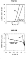
- FIGS. 8A and 8B show forward characteristics and reverse characteristics of the newly made trench MOS Schottky barrier diode as Comparative Example and of the normal Schottky barrier diode.
- the turn-on voltage of the trench MOS Schottky barrier diode is larger in FIG. 8A than in FIG. 7A . It is considered that this is because the treatment with the sulfuric acid/hydrogen peroxide mixture after the treatment with the buffered hydrofluoric acid was omitted in the pre-treatment before deposition of the Cu/Au/Ni laminated film.
- the leakage current in the trench MOS Schottky barrier diode is several orders of magnitude less than the leakage current in the normal Schottky barrier diode in the similar manner to that in FIG. 7B but, from the viewpoint of withstand voltage, the electrode was broken at about 175 V in the trench MOS Schottky barrier diode and at about 90 V in the normal Schottky barrier diode. When the broken electrodes were observed, it was found that breakdown occurred at the end portion of the electrode in both the normal Schottky barrier diode and the trench MOS Schottky barrier diode.
- a trench MOS Schottky barrier diode having a field-plate structure was made.
- a sample having a field-plate structure and not having trenches was also made on the same epi-wafer.
- FIG. 9 is a vertical cross-sectional view showing a trench MOS Schottky barrier diode 3 having a field-plate structure in Example 4.
- a dielectric layer 31 formed of SiO 2 is provided on the surface 27 of the first semiconductor layer 20 so as to be located around an anode electrode 32, and the edge of an anode electrode 32 rides over the dielectric layer 31.
- FIGS. 10A and 10B show forward characteristics and reverse characteristics of the trench MOS Schottky barrier diode 3 in Example 4 and of the normal Schottky barrier diode in Comparative Example.
- FIG. 10B shows that withstand voltage of the trench MOS Schottky barrier diode is increased to about 450 V by providing the field-plate structure.
- the orientation of the linear trenches is preferably parallel to the [010] direction of the Ga 2 O 3 -based single crystal constituting the first semiconductor layer 20.
- a thickness of the damage layer on the inner surfaces of the trenches 22 (on the surfaces of the mesa-shaped portions) produced by dry etching performed to form the trenches 22 is around 0.5 ⁇ m and it is preferable to remove the damage layer by treating with phosphoric acid.
- a Schottky barrier diode is provided which is formed using a Ga 2 O 3 -based semiconductor and has a lower turn-on voltage than the known Schottky barrier diodes.
Landscapes
- Electrodes Of Semiconductors (AREA)
Abstract
Description
- The invention relates to a Schottky barrier diode.
- A Schottky barrier diode, in which a Schottky electrode formed of Pt is connected to a Ga 2 O 3 single crystal, is known (see, e.g., Non-Patent Literature 1). The turn-on voltage (forward voltage) of the Schottky barrier diode described in
Non-Patent Literature 1 is 1.23 V. - Also, a Schottky barrier diode, in which a Schottky electrode having a Ni/Au laminated structure is connected onto a Ga 2 O 3 single crystal, is known (see, e.g., Non-Patent Literature 2).
- Also, a trench MOS Schottky barrier diode using Si as a semiconductor layer and a trench MOS Schottky barrier diode using SiC as a semiconductor layer are known (e.g., Non-Patent
Literatures 3 and 4). -
- Non-Patent Literature 1: Kohei Sasaki et al., "Ga2O3 Schottky Barrier Diodes Fabricated by Using Single-Crystal β-Ga2O3 (010) Substrates", IEEE Electron Device Letters, April 2013, Vol.34, No.4, pp.493-495 .
- Non-Patent Literature 2: Toshiyuki Oishi et al., "Conduction mechanism in highly doped β-Ga2O3 (-201) single crystals grown by edge-defined film-fed growth method and their Schottky barrier diodes", Japanese Journal of Applied Physics, 2016, 55, 030305 .
- Non-Patent Literature 3: T. Shimizu et al., Proceedings of 2001 International Symposium on Power Semiconductor Devices & ICs, Osaka, pp.243-246 (2001)
- Non-Patent Literature 4: V. Khemka, et al., IEEE ELECTRON DEVICE LETTERS, VOL.21, NO.5, MAY 2000, pp.286-288
- In general, it is necessary to change the turn-on voltage of Schottky barrier diode according to the intended use thereof. Schottky barrier diode having a Ga 2 O 3 -based semiconductor layer is also required to have a turn-on voltage in a range different from the known Schottky barrier diodes, particularly, to have a low turn-on voltage so that forward loss can be kept low.
- Thus, it is an object of the invention to provide a Schottky barrier diode which is formed using a Ga 2 O 3 -based semiconductor and has a lower turn-on voltage (a lower rising voltage) than the known Schottky barrier diodes.
- To achieve the above-mentioned object, an aspect of the invention provides a Schottky barrier diode according to [1] to [6] below.
- [1] A Schottky barrier diode, comprising: a first semiconductor layer comprising a Ga 2 O 3 -based single crystal; an anode electrode which forms a Schottky junction with the first semiconductor layer and whose portion to contact with the first semiconductor layer comprises Fe or Cu; and a cathode electrode.
- [2] The Schottky barrier diode according to [1], wherein the portion of the anode electrode to contact with the first semiconductor layer comprises Fe, and a turn-on voltage is not less than 0.4 V and not more than 0.5 V.
- [3] The Schottky barrier diode according to [1], wherein the portion of the anode electrode to contact with the first semiconductor layer comprises Cu, and a turn-on voltage is not less than 0.6 V and not more than 0.7 V.
- [4] The Schottky barrier diode according to [1], comprising: a second semiconductor layer that comprises a Ga 2 O 3 -based single crystal and is laminated on the first semiconductor layer, wherein the first semiconductor layer comprises trenches opening on a surface opposite to the second semiconductor layer, inner surfaces of the trenches are covered with insulating films, and trench MOS barriers are embedded in the trenches so as to be covered with the insulating films, wherein the anode electrode is to contact with the trench MOS barriers, and the cathode electrode is connected to the second semiconductor layer.
- [5] The Schottky barrier diode according to [4], wherein the portion of the anode electrode to contact with the first semiconductor layer comprises Fe, and a turn-on voltage is not less than 0.4 V and not more than 0.7 V.
- [6] The Schottky barrier diode according to [4], wherein the portion of the anode electrode to contact with the first semiconductor layer comprises Cu, and a turn-on voltage is not less than 0.6 V and not more than 0.9 V.
- According to the invention, it is possible to provide a Schottky barrier diode which is formed using a Ga 2 O 3 -based semiconductor and has a lower turn-on voltage than the known Schottky barrier diodes.
-
-
FIG. 1 is a vertical cross-sectional view showing a Schottkybarrier diode 1 in the first embodiment. -
FIG. 2A is a vertical cross-sectional view showing a trench MOS Schottky barrier diode in the second embodiment. -
FIG. 2B is an enlarged view showing the vicinity of a trench when trench MOS barriers and an anode electrode are formed integrally. -
FIG. 3A is a vertical cross-sectional view showing a process of manufacturing the trench MOS Schottky barrier diode in the second embodiment. -
FIG. 3B is a vertical cross-sectional view showing the process of manufacturing the trench MOS Schottky barrier diode in the second embodiment. -
FIG. 3C is a vertical cross-sectional view showing the process of manufacturing the trench MOS Schottky barrier diode in the second embodiment. -
FIG. 4A is a vertical cross-sectional view showing the process of manufacturing the trench MOS Schottky barrier diode in the second embodiment. -
FIG. 4B is a vertical cross-sectional view showing the process of manufacturing the trench MOS Schottky barrier diode in the second embodiment. -
FIG. 4C is a vertical cross-sectional view showing the process of manufacturing the trench MOS Schottky barrier diode in the second embodiment. -
FIG. 5 is a graph showing a relation between a material of the anode electrode and a turn-on voltage of the Schottky barrier diode in Example 1. -
FIG. 6A is a graph showing a relation between a material of the anode electrode and a turn-on voltage of the trench MOS Schottky barrier diode in Example 2. -
FIG. 6B is a graph showing a relation between a type of pre-treatment solution and a turn-on voltage in Example 2. -
FIG. 7A shows forward characteristics of a trench MOS Schottky barrier diode in Example 4 and of a normal Schottky barrier diode in Comparative Example. -
FIG. 7B shows reverse characteristics of the trench MOS Schottky barrier diode in Example 4 and of the normal Schottky barrier diode in Comparative Example. -
FIG. 8A shows forward characteristics of a trench MOS Schottky barrier diode as Comparative Example and of the normal Schottky barrier diode. -
FIG. 8B shows reverse characteristics of the trench MOS Schottky barrier diode as Comparative Example and of the normal Schottky barrier diode. -
FIG. 9 is a vertical cross-sectional view showing a trench MOS Schottky barrier diode having a field-plate structure in Example 4. -
FIG. 10A shows forward characteristics of the trench MOS Schottky barrier diode in Example 4 and of the normal Schottky barrier diode in Comparative Example. -
FIG. 10B shows reverse characteristics of the trench MOS Schottky barrier diode in Example 4 and of the normal Schottky barrier diode in Comparative Example. -
FIG. 1 is a vertical cross-sectional view showing a Schottkybarrier diode 1 in the first embodiment. The Schottkybarrier diode 1 is a vertical Schottky barrier diode and has asemiconductor layer 10, ananode electrode 11 formed on one surface of thesemiconductor layer 10, and acathode electrode 12 formed on another surface of thesemiconductor layer 10. - The
semiconductor layer 10 is a plate-shaped member formed of a Ga 2 O 3 -based single crystal and is typically a Ga 2 O 3 -based substrate. Thesemiconductor layer 10 may be undoped (with no intentional doping) or may contain a dopant such as Si or Sn. A carrier concentration of thesemiconductor layer 10 is preferably, e.g., not less than 1x1015 cm -3 and not more than 1x1018 cm -3 . - The Ga 2 O 3 -based single crystal here means a Ga 2 O 3 single crystal or is a Ga 2 O 3 single crystal doped with an element such as Al or In, and may be, e.g., a (GaxAlyIn(1-x-y)) 2 O 3 (0<x≤1, 0≤y<1, 0<x+y≤1) single crystal which is a Ga 2 O 3 single crystal doped with Al and In. The band gap is widened by adding Al and is narrowed by adding In. The Ga 2 O 3 single crystal mentioned above has, e.g., a β-crystal structure.
- A thickness of the
semiconductor layer 10 is preferably not less than 100 nm so that theSchottky barrier diode 1 can have sufficient withstand voltage characteristics. Withstand voltage of theSchottky barrier diode 1 is determined by the thickness and carrier concentration of thesemiconductor layer 10. There is no specific upper limit for the thickness of thesemiconductor layer 10. On the other hand, since electrical resistance in the thickness direction increases with an increase in the thickness, thesemiconductor layer 10 is preferably as thin as possible provided that the required withstand voltage characteristics are obtained. - The
semiconductor layer 10 may alternatively have a multilayer structure composed of two or more Ga 2 O 3 -based single crystal layers. In this case, thesemiconductor layer 10 is composed of, e.g., a Ga 2 O 3 -based single crystal substrate and a Ga 2 O 3 -based single crystal film epitaxially grown thereon. In case that theanode electrode 11 is connected to the Ga 2 O 3 -based single crystal film and thecathode electrode 12 is connected to the Ga 2 O 3 -based single crystal substrate, for example, the carrier concentration of the Ga 2 O 3 -based single crystal film is set to not less than 1x1015 cm -3 and not more than 1x1017 cm -3 and the carrier concentration of the Ga 2 O 3 -based single crystal substrate is set to not less than 1x1017 cm -3 and not more than 4x1019 cm -3 . - The
anode electrode 11 is configured so that a portion to contact with thesemiconductor layer 10 is formed of Fe or Cu. In detail, theanode electrode 11 when having a single layer structure is entirely formed of Fe or Cu, and theanode electrode 11 when having a multilayer structure is configured so that a layer to contact with thesemiconductor layer 10 is formed of Fe or Cu. In both cases, a Schottky barrier is formed at an interface between the Fe or Cu portion of theanode electrode 11 and thesemiconductor layer 10, and a Schottky junction is formed between theanode electrode 11 and thesemiconductor layer 10. - When the portion of the
anode electrode 11 to contact with thesemiconductor layer 10 is formed of Fe, the turn-on voltage of theSchottky barrier diode 1 is not less than 0.4V and not more than 0.5V. Meanwhile, when the portion of theanode electrode 11 to contact with thesemiconductor layer 10 is formed of Cu, the turn-on voltage of theSchottky barrier diode 1 is not less than 0.6V and not more than 0.7V. - The thickness of the Fe or Cu portion of the
anode electrode 11 is preferably not less than 10 nm. When the thickness is less than 10 nm, pinholes may be formed and good rectifying properties may not be obtained. In contrast, when the Fe or Cu portion of theanode electrode 11 has a thickness of not less than 10 nm, good rectifying properties are obtained and differential on-resistance after the current value started to rise is reduced. - There is no upper limit for the thickness of the Fe or Cu portion of the
anode electrode 11 in terms of performance of element. - When the
anode electrode 11 has a laminated structure, e.g., an Au layer is laminated on a layer formed of Fe or Cu. The Au layer is used to reduce wiring resistance of the electrode itself. The thicker Au layer is better for reducing the wiring resistance, but the thickness of the Au layer is preferably not more than 5000 nm in view of the manufacturing cost. - The
cathode electrode 12 is configured so that a portion to contact with thesemiconductor layer 10 is formed of a metal such as Ti forming an ohmic junction with Ga 2 O 3 -based single crystal and forms an ohmic junction with thesemiconductor layer 10. That is, thecathode electrode 12 when having a single layer structure is entirely formed of Ti, etc., and thecathode electrode 12 when having a multilayer structure is configured so that a layer to contact with thesemiconductor layer 10 is formed of Ti, etc. Examples of the multilayer structure of thecathode electrode 12 include Ti/Au and Ti/Al. - In the
Schottky barrier diode 1, an energy barrier at an interface between theanode electrode 11 and thesemiconductor layer 10 as viewed from thesemiconductor layer 10 is lowered by applying forward voltage between theanode electrode 11 and the cathode electrode 12 (positive potential on theanode electrode 11 side), allowing an electric current to flow from theanode electrode 11 to thecathode electrode 12. On the other hand, when reverse voltage is applied between theanode electrode 11 and the cathode electrode 12 (negative potential on theanode electrode 11 side), the electric current does not flow due to the Schottky barrier. - An example of a method for manufacturing the
Schottky barrier diode 1 will be described below. - Firstly, a bulk crystal of a Ga 2 O 3 -based single crystal grown by a melt-growth technique such as the FZ (Floating Zone) method or the EFG (Edge Defined Film Fed Growth) method is sliced and the surface thereof is then polished, thereby forming a Ga 2 O 3 -based substrate as the
semiconductor layer 10. - Next, the front and back surfaces of the
semiconductor layer 10 are pre-treated with a sulfuric acid/hydrogen peroxide mixture (e.g., with a volume ratio of sulfuric acid: hydrogen peroxide: water = 4:1:1). In case that a treatment solution other than the sulfuric acid/hydrogen peroxide mixture, such as hydrochloric acid, nitric acid, sulfuric acid, hydrofluoric acid or buffered hydrofluoric acid, is used, treatment with the sulfuric acid/hydrogen peroxide mixture is performed after treatment with such solution. If treatment with the sulfuric acid/hydrogen peroxide mixture is not performed at the end of the pre-treatment, it could cause the turn-on voltage of theSchottky barrier diode 1 to be fixed to about 0.8V to 1.0V, regardless of the material of theanode electrode 11. - Next, the
anode electrode 11 and thecathode electrode 12 are respectively formed on the front and back surfaces of thesemiconductor layer 10 by vacuum deposition, etc. Theanode electrode 11 may be patterned into a predetermined shape such as circle by photo etching, etc. -
FIG. 2A is a vertical cross-sectional view showing a trench MOSSchottky barrier diode 2 in the second embodiment. The trench MOSSchottky barrier diode 2 is a vertical Schottky barrier diode having a trench MOS region. - The trench MOS
Schottky barrier diode 2 has afirst semiconductor layer 20, asecond semiconductor layer 21 laminated thereon, ananode electrode 23 connected to thefirst semiconductor layer 20, and acathode electrode 24 connected to thesecond semiconductor layer 21. - The
first semiconductor layer 20 hastrenches 22 opening on asurface 27 opposite to thesecond semiconductor layer 21. Inner surfaces of thetrenches 22 are covered with insulatingfilms 25, andtrench MOS barriers 26 are embedded in thetrenches 22 so as to be covered with the insulatingfilms 25. Theanode electrode 23 is to contact with thetrench MOS barriers 26. - In the trench MOS
Schottky barrier diode 2, an energy barrier at an interface between theanode electrode 23 and thefirst semiconductor layer 20 as viewed from thefirst semiconductor layer 20 is lowered by applying forward voltage between theanode electrode 23 and the cathode electrode 24 (positive potential on theanode electrode 23 side), allowing an electric current to flow from theanode electrode 23 to thecathode electrode 24. - On the other hand, when reverse voltage is applied between the
anode electrode 23 and the cathode electrode 24 (negative potential on theanode electrode 23 side), the electric current does not flow due to the Schottky barrier. When reverse voltage is applied between theanode electrode 23 and thecathode electrode 24, a depletion layer spreads from an interface between theanode electrode 23 and thefirst semiconductor layer 20 and from an interface between the insulatingfilms 25 and thefirst semiconductor layer 20. - In general, the upper limit of reverse leakage current in Schottky diode is 1 µA. In the embodiment, reverse voltage when a leakage current of 1 µA flows is defined as withstand voltage.
- According to data of dependence of reverse leakage current on electric field strength at Schottky interface in Schottky diode having a SiC semiconductor layer described in, e.g., "Technology of Semiconductor SiC and its Application" by Hiroyuki Matsunami, Noboru Otani, Tsunenobu Kimoto und Takashi Nakamura, Second Edition, Nikkan Kogyo Shimbun, Ltd., September 30, 2011, p.355 , electric field strength immediately under Schottky electrode is about 0.8 MV/cm when a current density of reverse leakage current is 0.0001 A/cm 2 . 0.0001 A/cm 2 here is a current density immediately under the Schottky electrode when an electric current of 1 µA flows through the Schottky electrode having a size of 1 mm × 1 mm.
- Thus, even when breakdown field strength of the semiconductor material itself is several MV/cm, a leakage current of more than 1 µA flows when the electric field strength immediately under the Schottky electrode exceeds 0.8 MV/cm.
- In order to obtain withstand voltage of 1200V in, e.g., a known Schottky diode not having a special structure to reduce electric field strength immediately under Schottky electrode, a donor concentration in a semiconductor layer needs to be reduced to the order of 1015 cm -3 and also the semiconductor layer needs to be very thick so that the electric field strength immediately under the Schottky electrode is kept not more than 0.8 MV/cm. This causes a significant increase in conduction loss, and it is thus difficult to make a Schottky barrier diode having a high withstand voltage and low loss.
- The trench MOS
Schottky barrier diode 2 in the second embodiment has a trench MOS structure and thus can have a high withstand voltage without an increase in resistance of the semiconductor layer. In other words, the trench MOSSchottky barrier diode 2 is a Schottky diode having a high withstand voltage and low loss. - Junction barrier Schottky (JBS) diode is known as a Schottky diode having a high withstand voltage and low loss. However, Ga 2 O 3 is not suitable as a material for the JBS diode requiring a p-type region since it is difficult to manufacture p-type Ga 2 O 3 .
- The
second semiconductor layer 21 is formed of an n-type Ga 2 O 3 -based single crystal containing a Group IV element, such as Si or Sn, as a donor. A donor concentration of thesecond semiconductor layer 21 is, e.g., not less than 1.0x10¹⁸ and not more than 1.0x1020 cm -3 . A thickness Ts of thesecond semiconductor layer 21 is, e.g., 10 to 600 µm. Thesecond semiconductor layer 21 is, e.g., a Ga2O3-based single crystal substrate. - The
first semiconductor layer 20 is formed of an n-type Ga 2 O 3 -based single crystal containing a Group IV element, such as Si or Sn, as a donor. A donor concentration of thefirst semiconductor layer 20 is lower than the donor concentration of thesecond semiconductor layer 21. Thefirst semiconductor layer 20 is, e.g., an epitaxial layer epitaxially grown on thesecond semiconductor layer 21 which is a Ga2O3-based single crystal substrate. - A high-donor-concentration layer containing a high concentration of donor may be additionally formed between the
first semiconductor layer 20 and thesecond semiconductor layer 21. In other words, thefirst semiconductor layer 20 and thesecond semiconductor layer 21 are laminated via the high-donor-concentration layer. The high-donor-concentration layer is used when, e.g., thefirst semiconductor layer 20 is epitaxially grown on thesecond semiconductor layer 21 as a substrate. At the early growth stage of thefirst semiconductor layer 20, the amount of dopant incorporated thereinto is unstable and an acceptor impurity is diffused from thesecond semiconductor layer 21 as a substrate. Thus, in some cases, resistance increases in a region of thefirst semiconductor layer 20 close to the interface with thesecond semiconductor layer 21 when thefirst semiconductor layer 20 is grown directly on thesecond semiconductor layer 21. The high-donor-concentration layer is used to avoid such problems. The concentration in the high-donor-concentration layer is set to be, e.g., higher than the concentration in thefirst semiconductor layer 20, more preferably, higher than the concentration in thesecond semiconductor layer 21. - As the donor concentration in the
first semiconductor layer 20 increases, electrical field strength in each part of the trench MOSSchottky barrier diode 2 increases. The donor concentration in thefirst semiconductor layer 20 is preferably not more than about 1.0x1017 cm-3 to lower the maximum electric field strength in a region of thefirst semiconductor layer 20 immediately under theanode electrode 23, the maximum electric field strength in thefirst semiconductor layer 20 and the maximum electric field strength in the insulatingfilm 25. On the other hand, as the donor concentration decreases, resistance of thefirst semiconductor layer 20 increases and the forward loss increases. Therefore, to obtain withstand voltage of, e.g., not more than 1200V, the donor concentration is preferably not less than 3.0x1016 cm -3 . To obtain higher withstand voltage, the donor concentration may be reduced to, e.g., about 1.0x1016 cm -3 . - As a thickness Te of the
first semiconductor layer 20 increases, the maximum electric field strength in thefirst semiconductor layer 20 and the maximum electric field strength in the insulatingfilm 25 decrease. By adjusting the thickness Te of thefirst semiconductor layer 20 to not less than about 3 µm, it is possible to effectively reduce the maximum electric field strength in thefirst semiconductor layer 20 and the maximum electric field strength in the insulatingfilm 25. In view of reduction in these maximum electric field strengths and downsizing of the trench MOSSchottky barrier diode 2, the thickness Te of thefirst semiconductor layer 20 is preferably about not less than 3 µm and not more than 9 µm. - Electrical field strength in each part of the trench MOS
Schottky barrier diode 2 changes depending on a depth Dt of thetrench 22. The depth Dt of thetrench 22 is preferably about not less than 1.5 µm and not more than 6 µm to lower the maximum electric field strength in a region of thefirst semiconductor layer 20 immediately under theanode electrode 23, the maximum electric field strength in thefirst semiconductor layer 20 and the maximum electric field strength in the insulatingfilm 25. - When a width Wt of the
trench 22 is narrower, the conduction loss can be more reduced but it is more difficult to manufacture, causing a decrease in production yield. Therefore, the width Wt is preferably not less than 0.3 µm and not more than 5 µm. - As a width Wm of a mesa-shaped portion between
adjacent trenches 22 on thefirst semiconductor layer 20 decreases, the maximum electric field strength in a region of thefirst semiconductor layer 20 immediately under theanode electrode 23 decreases. The width Wm of the mesa-shaped portion is preferably not more than 4 µm to lower the maximum electric field strength in a region of thefirst semiconductor layer 20 immediately under theanode electrode 23. At the same time, the width Wm of the mesa-shaped portion is preferably not less than 0.25 µm since it is more difficult to make thetrenches 22 when the width of the mesa-shaped portion is smaller. - Since the maximum electric field strength in the insulating
film 25 decreases as permittivity of the insulatingfilm 25 increases, the insulatingfilm 25 is preferably formed of a high-permittivity material. For example, Al 2 O 3 (relative permittivity of about 9.3) and HfO 2 (relative permittivity of about 22) can be used as a material of the insulatingfilm 25, and it is particularly preferable to use HfO 2 which has high permittivity. - Meanwhile, as a thickness Ti of the insulating
film 25 increases, the maximum electric field strength in thefirst semiconductor layer 20 decreases but the maximum electric field strength in the insulatingfilm 25 and the maximum electric field strength in a region immediately under theanode electrode 23 increase. In view of ease of manufacturing, the thickness of the insulatingfilm 25 is preferably smaller, and is more preferably not more than 300 nm. It is, however, obvious that a certain thickness is required so that an electric current virtually does not flow directly between thetrench MOS barrier 26 and thesecond semiconductor layer 20. - The
anode electrode 23 is configured so that a portion to contact with thefirst semiconductor layer 20 is formed of Fe or Cu, and theanode electrode 23 is in Schottky contact with thefirst semiconductor layer 20. - The material of the
trench MOS barrier 26 is not specifically limited as long as it is electrically conductive, and it is possible to use, e.g., polycrystalline Si doped at a high concentration and a metal such as Ni or Au. However, when thetrench MOS barriers 26 and theanode electrode 23 are formed integrally as shown inFIG. 2A , the surface layer of eachtrench MOS barrier 26 is also formed of Fe or Cu since the portion of theanode electrode 23 to contact with thefirst semiconductor layer 20 is formed of Fe or Cu. -
FIG. 2B is an enlarged view showing the vicinity of thetrench 22 when thetrench MOS barriers 26 and theanode electrode 23 are formed integrally. Theanode electrode 23 has afirst layer 23a to contact with thefirst semiconductor layer 20, and asecond layer 23b formed thereon. Thetrench MOS barrier 26 has afirst layer 26a to contact with the insulatingfilm 25, and asecond layer 26b formed thereon. - The
first layer 23a of theanode electrode 23 and thefirst layer 26a of thetrench MOS barrier 26 are formed as a continuous single film of Fe or Cu. Likewise, thesecond layer 23b of theanode electrode 23 and thesecond layer 26b of thetrench MOS barrier 26 are formed as a continuous single film of a conductive material such as Au. - Here, in case that the
first layer 26a of thetrench MOS barrier 26 is formed of Cu and is thick to the extent that thetrench MOS barrier 26 consists of only thefirst layer 26a, a gap is formed between thetrench MOS barrier 26 and the insulatingfilm 25 due to contraction of Cu. Therefore, to prevent a decrease in reliability of the trench MOSSchottky barrier diode 2, it is preferable that thetrench MOS barrier 26 be composed of thefirst layer 26a and thesecond layer 26b, i.e., it is preferable that thefirst layer 26a and thesecond layer 26b be embedded in thetrench 22. - When the portion of the
anode electrode 23 to contact with the first semiconductor layer 20 (i.e., thefirst layer 23a) is formed of Fe, the turn-on voltage of the trench MOSSchottky barrier diode 2 is not less than 0.4V and not more than 0.7V Meanwhile, when the portion of theanode electrode 23 to contact with the first semiconductor layer 20 (i.e., thefirst layer 23a) is formed of Cu, the turn-on voltage of the trench MOSSchottky barrier diode 2 is not less than 0.6V and not more than 0.9V. The turn-on voltage is slightly higher than that of theSchottky barrier diode 1 in the first embodiment even though the anode electrode material is the same, because the trench MOS structure causes a potential barrier to be formed in the mesa-shaped portion. This is determined by the width Wm of the mesa-shaped portion, such that the smaller the width Wm, the higher the turn-on voltage. - The electric field strength in the trench MOS
Schottky barrier diode 2 is affected by the width of the mesa-shaped portion between twoadjacent trenches 22, the depth Dt of thetrench 22 and the thickness Ti of the insulatingfilm 25, etc., as described above but is hardly affected by the planar pattern of thetrenches 22. Therefore, the planar pattern of thetrenches 22 on thefirst semiconductor layer 20 is not specifically limited. - The
cathode electrode 24 is in in ohmic contact with thesecond semiconductor layer 21. Thecathode electrode 24 is formed of a metal such as Ti. Thecathode electrode 24 may have a multilayer structure formed by laminating different metal films, e.g., Ti/Au or Ti/Al. For reliable ohmic contact between thecathode electrode 24 and thesecond semiconductor layer 21, thecathode electrode 24 is preferably configured that a layer to contact with thesecond semiconductor layer 21 is formed of Ti. - An example of a method for manufacturing the trench MOS
Schottky barrier diode 2 will be described below. -
FIGS. 3A to 3C and 4A to 4C are vertical cross-sectional views showing a process of manufacturing the trench MOSSchottky barrier diode 2 in the second embodiment. - Firstly, as shown in
FIG. 3A , a Ga 2 O 3 -based single crystal is epitaxially grown on thesecond semiconductor layer 21 such as a Ga 2 O 3 -based single crystal substrate by the HVPE (Hydride Vapor Phase Epitaxy) method, etc., thereby forming thefirst semiconductor layer 20. - Next, as shown in
FIG. 3B , thetrenches 22 are formed on the upper surface of thefirst semiconductor layer 20 by photo etching, etc. - In case that dry etching is used to form the
trenches 22, the preferable conditions are, e.g., use of BCl 3 (30 sccm) as an etching gas, pressure of 1.0 Pa, antenna power of 160W, bias power of 17W, and duration of 90 minutes. - Treatment with phosphoric acid is preferably performed after forming the
trenches 22 to remove roughness from inner surfaces of the trenches. Typically, immersion in phosphoric acid heated to 130 to 140°C for 5 to 30 minutes is preferable. - Next, as shown in
FIG. 3C , the insulatingfilm 25 made of HfO2, etc., is formed on the upper surface of thefirst semiconductor layer 20 by the ALD (Atomic Layer Deposition) method., etc., so that the inner surfaces of thetrenches 22 are covered. The conditions for HfO2 film formation are not specifically limited, and the film is formed by, e.g., alternately supplying TDMAH as an Hf raw material for 0.25 seconds and O 3 as an oxidizing agent for 0.15 seconds. The substrate temperature at this time is 250°C. - Next, as shown in
FIG. 4A , part of the insulatingfilm 25 outside the trenches 22 (portions located on the mesa-shaped portions between the trenches 22) is removed by a planarization process such as CMP (Chemical Mechanical Polishing). - Next, as shown in
FIG. 4B , thetrench MOS barriers 26 and theanode electrode 23, which have a Cu/Au/Ni laminated structure, etc., are formed continuously and integrally by electron beam evaporation, etc. - Before depositing the
trench MOS barriers 26 and theanode electrode 23, treatment with a sulfuric acid/hydrogen peroxide mixture is performed to remove CMP abrasive, etc. When a treatment solution other than the sulfuric acid/hydrogen peroxide mixture, such as hydrochloric acid, nitric acid, sulfuric acid, hydrofluoric acid or buffered hydrofluoric acid, is used, treatment with the sulfuric acid/hydrogen peroxide mixture is performed after treatment with such solution to prevent the turn-on voltage from being fixed to about 0.8 to 1.0V. - Next, as shown in
FIG. 4C , theanode electrode 23 is patterned into a predetermined shape such as circle by photo etching, etc. - After that, the
cathode electrode 24 having a Ti/Au laminated structure, etc., is formed on the bottom surface of thesecond semiconductor layer 21 by electron beam evaporation, etc., thereby obtaining the trench MOSSchottky barrier diode 2. - In the first and second embodiments, by using Fe or Cu as the material of the anode electrode which serves as a Schottky electrode, Schottky barrier diode having a semiconductor layer formed of a Ga 2 O 3 -based single crystal can have a lower turn-on voltage than the known Schottky barrier diodes.
- Using Schottky barrier diodes having the same structure as the
Schottky barrier diode 1 in the first embodiment, change in turn-on voltage when the material of the anode electrode serving as a Schottky electrode is different was examined. - In Example 1, a 650 µm-thick Ga 2 O 3 substrate which was undoped (with no intentionally added donor) and had a donor concentration of not more than 1x1017 cm-3 was used as the semiconductor layer.
- A circular electrode having a diameter of 200 µm was formed as the anode electrode by electron beam evaporation. Before depositing the anode electrode, the surface of the semiconductor layer was treated with a sulfuric acid/hydrogen peroxide mixture. Al, Ag, Fe, Cu, Ni, Pt and Pd were used as the anode electrode material.
- Then, an electrode having a Ti/Au laminated structure was formed as the cathode electrode on the entire back surface of the semiconductor layer by electron beam evaporation.
- Firstly, the turn-on voltage was measured on the Schottky barrier diodes respectively having the anode electrodes formed of different materials.
-
FIG. 5 is a graph showing a relation between a material of the anode electrode and a turn-on voltage of the Schottky barrier diode in Example 1. -
FIG. 5 shows that the turn-on voltages of the Schottky barrier diodes, when the anode electrode material is Al, Ag, Fe, Cu, Ni, Pt and Pd, are respectively about 0.0V, 0.3V, 0.5V, 0.6V, 0.8V, 0.95V and 0.95V. - Of those materials, Ni and Pt are known as materials of Schottky electrode to be to contact with semiconductor layer formed of Ga 2 O 3 -based single crystal. Fe and Cu provide different turn-on voltages from when using Ni and Pt and are thus usable as new Schottky electrode materials.
- When the anode electrode is formed of Fe, the turn-on voltage of the Schottky barrier diode, including variation, is not less than 0.4V and not more than 0.5V. Meanwhile, when the anode electrode is formed of Cu, the turn-on voltage of the Schottky barrier diode, including variation, is not less than 0.6V and not more than 0.7V.
- In a trench MOS Schottky barrier diode as is the trench MOS
Schottky barrier diode 2 in the second embodiment, reverse leakage is effectively reduced when the turn-on voltage is not less than 0.4V. This means that when using Fe or Cu as the anode electrode material, it is possible to lower the turn-on voltage while effectively reducing the reverse leakage. - Next, the Schottky barrier diodes respectively having the anode electrodes formed of Al, Ag, Fe, Cu, Ni and Pd were annealed to evaluate heat resistance of the anode electrode. The annealing temperature was increased to 200°C, 300°C and 400°C in this sequence, the annealing time was 10 minutes, and the annealing atmosphere was nitrogen.
- When the anode electrode material was Al, annealing at 200°C caused a hundredfold or more increase in conduction resistance, and annealing at 300°C caused an increase in the turn-on voltage to about 0.5V but conduction loss was recovered to the same level as immediately after deposition. Then, by annealing at 400°C, the turn-on voltage was lowered to about 0.4V and conduction loss was further increased about twofold.
- When the anode electrode material was Ag, annealing at 200°C caused roughness on the electrode surface and an increase in the turn-on voltage to about 0.5V. Annealing at 300°C caused an increase in the turn-on voltage to about 1.0 to 1.1V and a hundredfold or more increase in conduction resistance. Then, by annealing at 400°C, the Schottky barrier vanished and the characteristics changed to ohmic-like characteristics.
- When the anode electrode material was Fe, annealing at 100°C caused a hundredfold or more increase in conduction resistance, annealing at 200°C caused a little more increase in the resistance, and annealing at 300°C caused the characteristics to return to the level immediately after forming the electrode. Annealing at 400°C did not cause any change on the characteristics exhibited after annealing at 300°C. Based on these results, it is considered that the characteristics of the anode electrode formed of Fe can be stabilized by annealing at 300°C or 400°C after the electrode formation.
- When the anode electrode material was Cu, the turn-on voltage, which was about 0.6V immediately after deposition, was increased to about 0.7V by annealing at 200°C, was increased to about 0.9V by annealing at 300°C, and was further increased to about 1.1V annealing at 400°C.
- When the anode electrode material was Ni, no particular change was observed after annealing at 200°C and 300°C, but annealing at 400°C caused the conduction loss to rapidly increase about thousandfold.
- When the anode electrode material was Pd, the characteristics were similar to those when using Fe: annealing at 100°C caused a rapid increase in conduction resistance, annealing at 200°C caused a little more increase in the resistance, and annealing at 300°C caused the characteristics to return to the level immediately after forming the electrode. Annealing at 400°C did not cause any change on the characteristics exhibited after annealing at 300°C. Based on these results, it is considered that the characteristics of the anode electrode formed of Pd can be also stabilized by annealing at 300°C or 400°C after the electrode formation, in the same manner as the anode electrode formed of Fe.
- The above results show that the anode electrode formed of Ni exhibits a relatively small change with temperature increase and is excellent in heat resistance. On the other hand, it is also shown that the anode electrodes formed of Al, Ag and Cu exhibit unstable behavior with temperature increase and are less heat resistant. The anode electrodes formed of Fe and Pd exhibited a change with temperature increase but the characteristics thereof were stabilized by annealing at 300 to 400°C after deposition, and it is therefore considered that annealing after deposition can improve heat resistance up to the annealing temperature.
- Using trench MOS Schottky barrier diodes having the same structure as the trench MOS
Schottky barrier diode 2 in the second embodiment, change in turn-on voltage when the material of the anode electrode serving as a Schottky electrode is different was examined. - In Example 2, the surface of the semiconductor layer was treated with buffered hydrofluoric acid before depositing the anode electrode.
-
FIG. 6A is a graph showing a relation between a material of the anode electrode and a turn-on voltage of the trench MOS Schottky barrier diode in Example 2. -
FIG. 6A shows that the turn-on voltages of the Schottky barrier diodes, when the anode electrode material is Cu, Ni and Pt, are all in the range of 0.9 to 1.1V. - The result shown in
FIG. 6A is clearly different from the measurement result in Example 1, but it was found that the cause is that the buffered hydrofluoric acid was used in the pre-treatment before deposition of the anode electrode. This shows that the buffered hydrofluoric acid should not be used at the end of the pre-treatment before deposition of the anode electrode. - Next, a relation between the type of pre-treatment solution and the turn-on voltage was examined. Plural gallium oxide substrates were firstly prepared, were immersed respectively in hydrochloric acid, nitric acid, sulfuric acid, hydrofluoric acid, sulfuric acid/hydrogen peroxide mixture and buffered hydrofluoric acid for 5 minutes, and were then cleaned with running water. After that, a 200 µm-diameter, 200 nm-thick circular anode electrode formed of Cu and a cathode electrode composed of a 50 nm-thick Ti film and a 200 nm-thickAu film laminated on the Ti film were formed by vapor deposition.
-
FIG. 6B is a graph showing a relation between the type of pre-treatment solution and the turn-on voltage in Example 2. -
FIG. 6B shows that the turn-on voltage is as low as about 0.6 to 0.7V only when using the sulfuric acid/hydrogen peroxide mixture in the pre-treatment, and is fixed in the high turn-on voltage range when using hydrochloric acid, nitric acid, sulfuric acid, hydrofluoric acid or buffered hydrofluoric acid, i.e., when using a treatment solution other than the sulfuric acid/hydrogen peroxide mixture. - These results show that the turn-on voltage is prevented from being fixed in the high range by using the sulfuric acid/hydrogen peroxide mixture for the pre-treatment before formation of the anode electrode, or, when a solution other than sulfuric acid/hydrogen peroxide mixture is used, by treating with the sulfuric acid/hydrogen peroxide mixture after the treatment with such other solution.
- When forming a trench structure of the trench MOS Schottky barrier diode, a portion of the semiconductor layer formed of a Ga2O3-based single crystal, which should not be etched, needs to be protected by a masking material.
- SiO 2 , photoresist and Ni are often used as masking materials for dry etching. Of those, Ni is least likely to be etched and is the strongest as the masking material. However, since the Ga 2 O 3 -based single crystal is a material which is relatively difficult to etch, there is a problem that it is difficult to control selectivity even when Ni is used as the masking material.
- Based on this, a relation between the dry etching conditions for Ga 2 O 3 and the selectivity was investigated. Firstly, a mask formed of Ni was patterned on a Ga 2 O 3 substrate using photolithography technique. The obtained sample was dry-etched under four conditions shown in Table 1 below, and the selectivity of Ni to Ga 2 O 3 was evaluated.
Table 1 Gas Pressure Power (ICP/Bias) Time Condition 1 BCl 3 : 30 sccm 0.5 Pa 160W/ 17 W 5 minutes Condition 2 BCl 3 : 30 sccm 0.5 Pa 300W/ 50 W 5 minutes Condition 3 BCl 3 : 30 sccm 0.5 Pa 500W/ 80 W 5 minutes Condition 4 BCl 3 : 30 sccm 1.0 Pa 800W/250W 12.5 minutes - As a result of the evaluation, the selectivity under the condition 4 was 1 (the etch rate of Ni is the same as that of Ga 2 O 3 ) which shows that function of Ni as the mask is the lowest level, the selectivity under the
condition 3 was 5.8 (the etch rate of Ni is 1/5.8 of that of Ga 2 O 3 ), and the selectivity under thecondition 2 was 14.7. Meanwhile, the selectivity under thecondition 1 could not be quantified since Ni was hardly removed, but it was confirmed to be very high. Table 2 below summarizes the etch rate of Ga 2 O 3 under the respective conditions.Table 2 Etch rate Condition 1 28.2 nm/ min Condition 2 82.8 nm/ min Condition 3 130 nm/min Condition 4 194 nm/min - There was a clear correlation between the etch rate and the power, and the etch rate tended to be lower with lower power. Under the
condition 1 with which the selectivity to Ni was good, the etch rate was as low as 28.2 nm/min but was enough to be able to form trenches with a depth of several µm, which shows that thecondition 1 is the best etching condition in terms of both the selectivity and the etch rate. - The inside of the trenches formed by dry etching was also observed, and it was found that needle-like roughness occurred on the bottom and side surfaces of the trenches. In trench MOS Schottky barrier diode in which the electric field applied around the bottoms of the trenches is highest, such unevenness in shape may cause concentration of electric field, leading to breakdown at lower voltage than the designed withstand voltage. Therefore, the portion around the bottoms of the trenches is preferably smooth so that the electric field is uniform.
- Then, etching with phosphoric acid was experimentally performed to remove the needle-like product. A phosphoric acid was put in a glass beaker on a hot plate and was heated until the temperature reached 140°C, and then, a sample was immersed therein for 10 minutes. As a result, it was found that the needle-like roughness on the inner surfaces of the trenches on the Ga 2 O 3 substrate can be completely removed by phosphoric acid treatment.
- The trench MOS Schottky barrier diode in the second embodiment was made.
- Firstly, an Sn-doped Ga2O3 substrate having a thickness of 650 µm and a donor concentration of 2.5x1018 cm-3 was prepared as the
second semiconductor layer 21. The Sn-doped Ga 2 O 3 substrate was made by the EFG (Edge-defined, Film-fed Growth) method. - Next, an Si-doped Ga 2 O 3 film having a thickness of 7.5 µm and a donor concentration of 6x1016 cm-3 was homoepitaxially grown as the
first semiconductor layer 20 on the Sn-doped Ga 2 O 3 substrate by the HVPE method. - Next, a 300 nm-thick SiO 2 film was formed on the entire surface of the Si-doped Ga 2 O 3 film by sputter deposition, and a 200 nm-thick Ni film was formed thereon by electron beam evaporation. The Ni/SiO 2 laminated film was then patterned using photolithography technique.
- Next, using the patterned Ni/SiO 2 laminated film as a mask, linear trenches parallel to a [010] direction of the Si-doped Ga 2 O 3 film were formed as the
trenches 22 on the surface of the Si-doped Ga 2 O 3 film by an ICP-RIE system. The dry etching conditions were as follows: BCl 3 (30 sccm) as an etching gas, pressure of 0.5 Pa, antenna power of 160W, and bias power of 17W. The trenches had the depth Dt of about 3.0 µm and the width Wt of 4.8 µm, and the mesa-shaped portion had the width Wm of 1.2 µm. - After dry etching and the subsequent treatment with phosphoric acid at 140°C for 15 minutes, the sample was immersed in HF (46%) for 5 minutes to remove the SiO 2 film. Lastly, the sample was treated with the sulfuric acid/hydrogen peroxide mixture for 5 minutes to remove organic residues, etc., was cleaned with running water for 15 minutes, and was then dried by nitrogen blow.
- Next, a 50 nm-thick HfO 2 film was formed as the insulating
film 25 by ALD. At this time, an O 3 gas was used as an oxidizing agent. - Next, the surface of the Si-doped Ga 2 O 3 film was polished to a depth of about 0.5 µm by CMP, and the HfO 2 film on the mesa-shaped portions between the trenches was thereby removed. This resulted in the Si-doped Ga 2 O 3 film having a thickness of about 7.0 µm and the trench having the depth Dt of about 2.5 µm.
- Next, the back surface of the Sn-doped Ga 2 O 3 substrate was mirror-polished by diamond lapping and CMP. This resulted in the Sn-doped Ga 2 O 3 substrate having a thickness of 350 µm.
- Next, the sample was immersed in acetone and was treated therewith for 10 minutes while applying an ultrasonic wave. Then, the sample was immersed in a sulfuric acid/hydrogen peroxide mixture for 5 minutes and then in a buffered hydrofluoric acid for 1 minute, and was cleaned with running water for 15 minutes. Residues left over from cleaning or wax used to fix the sample at the time of polishing can be roughly removed by the acetone, organic matters can be removed by the sulfuric acid/hydrogen peroxide mixture, and colloidal silica contained in CMP slurry can be removed by the buffered hydrofluoric acid. Lastly, the sample was again immersed in the sulfuric acid/hydrogen peroxide mixture for 5 minutes, was cleaned with running water and was dried by nitrogen blow.
- Next, a 200 nm-thick Cu film, a 3.0 µm-thick Au film and a 50 nm-thick Ni film were laminated by electron beam evaporation, thereby forming a Cu/Au/Ni laminated film which serves as the
trench MOS barriers 26 as well as theanode electrode 23. The deposition rate was 0.3 to 0.4 nm/s. The Cu film and the Au film were embedded in the trenches. The Ni film as the outermost layer was formed to increase adhesion with photoresist used in the next step. - The Cu film may be penetrated by Au when too thin and may be separated from Au due to the difference in thermal expansion when too thick. For this reason, experiment was conducted under several different conditions. As a result, it was found that the preferable thickness of the Cu film is about 10 to 400 nm. Based on this finding, the Cu film in Example 4 was formed to have a thickness of 200 nm which is an intermediate value between 10 and 400 nm.
- Next, a photoresist was patterned on the Cu/Au/Ni laminated film which was then wet-etched using the photoresist as a mask. The sample was firstly treated with a mixture of nitric acid, hydrochloric acid and water (with a volume ratio of nitric acid: hydrochloric acid: water = 2:2:1) for 6 seconds to remove the Ni film, and was then immersed in AURUM-302 (manufactured by Kanto Chemical), which is an Au etchant, for about 2 hours. After that, ultrasonic cleaning in acetone was performed for 5 minutes to remove the photoresist. An anode electrode portion of the Cu/Au/Ni laminated film was thereby patterned into a circular shape with a diameter of 400 µm.
- Lastly, a 50 nm-thick Ti film and a 200 nm-thick Au film were formed on the entire back surface of the Sn-doped Ga 2 O 3 substrate by electron beam evaporation, and a Ti/Au laminated film as the
cathode electrode 24 was thereby formed. For the purpose of comparison, a sample without trenches (normal Schottky barrier diode) was also made on the same epi-wafer. -
FIG. 7A shows forward characteristics of the trench MOSSchottky barrier diode 2 in Example 4 and of the normal Schottky barrier diode in Comparative Example. In the drawing, "trench SBD" denotes the trench MOSSchottky barrier diode 2 and "SBD" denotes the normal Schottky barrier diode as Comparative Example in which trenches are not formed. -
FIG. 7A shows that the trench MOSSchottky barrier diode 2 has a higher on-resistance than the normal Schottky barrier diode. This is due to the fact that the electric current path is narrowed by providing the trench MOS structure, hence, it is a reasonable result. -
FIG. 7B shows reverse characteristics of the trench MOSSchottky barrier diode 2 in Example 4 and of the normal Schottky barrier diode in Comparative Example. While the normal Schottky barrier diode without trenches exhibits leakage characteristics substantially the same as predicted by the thermionic field emission theory, leakage current in the trench MOSSchottky barrier diode 2 is several orders of magnitude less than the normal Schottky barrier diode. This is because electric field strength at the Schottky junction portion was decreased by providing the trench MOS structure and leakage current due to thermionic field emission (TFE) was reduced. - Next, another trench MOS Schottky barrier diode was newly made by the same process, except that the last step of immersion in the sulfuric acid/hydrogen peroxide mixture and cleaning with running water was omitted in the pre-treatment before deposition of the Cu/Au/Ni laminated film formed as the
trench MOS barriers 26 and theanode electrode 23. The width Wt of trenches was 5 µm and the width Wm of the mesa-shaped portions was 1 µm. The Si-doped Ga 2 O 3 film was formed to have a donor concentration of 5x1016 cm-3 and a final thickness of 8.0 µm. For the purpose of comparison, a sample without trenches (normal Schottky barrier diode) subjected to the same pre-treatment was also made on the same epi-wafer. -
FIGS. 8A and 8B show forward characteristics and reverse characteristics of the newly made trench MOS Schottky barrier diode as Comparative Example and of the normal Schottky barrier diode. The turn-on voltage of the trench MOS Schottky barrier diode is larger inFIG. 8A than inFIG. 7A . It is considered that this is because the treatment with the sulfuric acid/hydrogen peroxide mixture after the treatment with the buffered hydrofluoric acid was omitted in the pre-treatment before deposition of the Cu/Au/Ni laminated film. - In
FIG. 8B , the leakage current in the trench MOS Schottky barrier diode is several orders of magnitude less than the leakage current in the normal Schottky barrier diode in the similar manner to that inFIG. 7B but, from the viewpoint of withstand voltage, the electrode was broken at about 175V in the trench MOS Schottky barrier diode and at about 90V in the normal Schottky barrier diode. When the broken electrodes were observed, it was found that breakdown occurred at the end portion of the electrode in both the normal Schottky barrier diode and the trench MOS Schottky barrier diode. - Next, to prevent breakdown from occurring at the end portion of the electrode and to improve withstand voltage, a trench MOS Schottky barrier diode having a field-plate structure was made. For the purpose of comparison, a sample having a field-plate structure and not having trenches (normal Schottky barrier diode) was also made on the same epi-wafer.
-
FIG. 9 is a vertical cross-sectional view showing a trench MOSSchottky barrier diode 3 having a field-plate structure in Example 4. In the trench MOSSchottky barrier diode 3, adielectric layer 31 formed of SiO2 is provided on thesurface 27 of thefirst semiconductor layer 20 so as to be located around ananode electrode 32, and the edge of ananode electrode 32 rides over thedielectric layer 31. -
FIGS. 10A and 10B show forward characteristics and reverse characteristics of the trench MOSSchottky barrier diode 3 in Example 4 and of the normal Schottky barrier diode in Comparative Example. -
FIG. 10B shows that withstand voltage of the trench MOS Schottky barrier diode is increased to about 450V by providing the field-plate structure. - Using the trench MOS
Schottky barrier diode 2 in Example 4 pertaining toFIG. 7 , a comparison was conducted between when thetrenches 22 were linear trenches parallel to the [010] direction of the Si-doped Ga 2 O 3 film serving as thefirst semiconductor layer 20 and were linear trenches parallel to a [100] direction. - After forming the trenches by dry etching so that the width Wm of the mesa-shaped portions between the trenches was 2.5 µm, treatment was performed with phosphoric acid, resulting in the mesa-shaped portions between the trenches parallel to the [010] direction having the width Wm of 1 to 1.5 µm and the mesa-shaped portions between the trenches parallel to the [100] direction having the width Wm of about 2 µm. It is considered that this is because the etch rate in phosphoric acid is different depending on the orientation of Ga 2 O 3 .
- After that, forward characteristics of the completed trench MOS
Schottky barrier diode 2 were evaluated. The results was that on-resistance of the diode having the linear trenches parallel to the [100] direction, in which the width Wm of the mesa-shaped portions is wide and the current path thus should be wide, was about 1.5 times to twice higher than on-resistance of the diode having liner trenches parallel to the [010] direction. - The reason is considered to be as follows: since the mesa-shaped portions between the linear trenches parallel to the [100] direction are hardly etched by the phosphoric acid as described above, damage due to dry etching remains and the effective current path is narrowed due to electric charge of the layer with the unremoved damage.
- This result shows that the orientation of the linear trenches is preferably parallel to the [010] direction of the Ga 2 O 3 -based single crystal constituting the
first semiconductor layer 20. In addition, it was also shown that a thickness of the damage layer on the inner surfaces of the trenches 22 (on the surfaces of the mesa-shaped portions) produced by dry etching performed to form thetrenches 22 is around 0.5 µm and it is preferable to remove the damage layer by treating with phosphoric acid. - Although the embodiments and Examples of the invention have been described, the invention is not intended to be limited to the embodiments and Examples, and the various kinds of modifications can be implemented without departing from the gist of the invention.
- In addition, the invention according to claims is not to be limited to the embodiments and Examples described above. Further, it should be noted that all combinations of the features described in the embodiments and Examples are not necessary to solve the problem of the invention.
- A Schottky barrier diode is provided which is formed using a Ga 2 O 3 -based semiconductor and has a lower turn-on voltage than the known Schottky barrier diodes.
-
- 1 SCHOTTKY BARRIER DIODE
- 2, 3 TRENCH MOS SCHOTTKY BARRIER DIODE
- 10 SEMICONDUCTOR LAYER
- 11, 23 ANODE ELECTRODE
- 12, 24 CATHODE ELECTRODE
- 20 FIRST SEMICONDUCTOR LAYER
- 21 SECOND SEMICONDUCTOR LAYER
- 22 TRENCH
- 25 INSULATING FILM
- 26 TRENCH MOS BARRIER
Claims (6)
- A Schottky barrier diode, comprising:a first semiconductor layer comprising a Ga 2 O 3 -based single crystal;an anode electrode which forms a Schottky junction with the first semiconductor layer and whose portion to contact with the first semiconductor layer comprises Fe or Cu; anda cathode electrode.
- The Schottky barrier diode according to claim 1, wherein the portion of the anode electrode to contact with the first semiconductor layer comprises Fe, and a turn-on voltage is not less than 0.4 V and not more than 0.5 V.
- The Schottky barrier diode according to claim 1, wherein the portion of the anode electrode to contact with the first semiconductor layer comprises Cu, and a turn-on voltage is not less than 0.6 V and not more than 0.7 V.
- The Schottky barrier diode according to claim 1, comprising a second semiconductor layer that comprises a Ga 2 O 3 -based single crystal and is laminated on the first semiconductor layer,wherein the first semiconductor layer comprises trenches opening on a surface opposite to the second semiconductor layer, inner surfaces of the trenches are covered with insulating films, and trench MOS barriers are embedded in the trenches so as to be covered with the insulating films,wherein the anode electrode is to contact with the trench MOS barriers, and the cathode electrode is connected to the second semiconductor layer.
- The Schottky barrier diode according to claim 4, wherein the portion of the anode electrode to contact with the first semiconductor layer comprises Fe, and a turn-on voltage is not less than 0.4 V and not more than 0.7 V.
- The Schottky barrier diode according to claim 4, wherein the portion of the anode electrode to contact with the first semiconductor layer comprises Cu, and a turn-on voltage is not less than 0.6 V and not more than 0.9 V.
Applications Claiming Priority (2)
| Application Number | Priority Date | Filing Date | Title |
|---|---|---|---|
| JP2017036995A JP6967238B2 (en) | 2017-02-28 | 2017-02-28 | Schottky barrier diode |
| PCT/JP2018/005665 WO2018159350A1 (en) | 2017-02-28 | 2018-02-19 | Schottky barrier diode |
Publications (3)
| Publication Number | Publication Date |
|---|---|
| EP3591711A1 true EP3591711A1 (en) | 2020-01-08 |
| EP3591711A4 EP3591711A4 (en) | 2020-12-09 |
| EP3591711B1 EP3591711B1 (en) | 2022-08-31 |
Family
ID=63371063
Family Applications (1)
| Application Number | Title | Priority Date | Filing Date |
|---|---|---|---|
| EP18761989.5A Active EP3591711B1 (en) | 2017-02-28 | 2018-02-19 | Schottky barrier diode |
Country Status (5)
| Country | Link |
|---|---|
| US (1) | US11043602B2 (en) |
| EP (1) | EP3591711B1 (en) |
| JP (1) | JP6967238B2 (en) |
| CN (1) | CN110326115B (en) |
| WO (1) | WO2018159350A1 (en) |
Cited By (1)
| Publication number | Priority date | Publication date | Assignee | Title |
|---|---|---|---|---|
| EP3654387A4 (en) * | 2017-07-08 | 2021-03-31 | Flosfia Inc. | SEMICONDUCTOR DEVICE |
Families Citing this family (18)
| Publication number | Priority date | Publication date | Assignee | Title |
|---|---|---|---|---|
| CN110809826B (en) * | 2017-06-29 | 2022-10-28 | 三菱电机株式会社 | Oxide semiconductor device and method for manufacturing oxide semiconductor device |
| JP7012306B2 (en) * | 2018-03-01 | 2022-01-28 | 株式会社タムラ製作所 | Trench MOS type Schottky diode and its manufacturing method |
| JP6966739B2 (en) * | 2018-10-23 | 2021-11-17 | Tdk株式会社 | Schottky barrier diode |
| JP2020155530A (en) * | 2019-03-19 | 2020-09-24 | トヨタ自動車株式会社 | Manufacturing method of semiconductor devices |
| US11476340B2 (en) * | 2019-10-25 | 2022-10-18 | Ohio State Innovation Foundation | Dielectric heterojunction device |
| JP7690157B2 (en) * | 2019-11-14 | 2025-06-10 | 株式会社Flosfia | Semiconductor Device |
| WO2021095474A1 (en) * | 2019-11-14 | 2021-05-20 | 株式会社Flosfia | Method for etching crystalline oxide, method for forming trench, and method for producing semiconductor device |
| JP2021082711A (en) * | 2019-11-19 | 2021-05-27 | 株式会社デンソー | Manufacturing method of semiconductor device |
| JP7415537B2 (en) * | 2019-12-18 | 2024-01-17 | Tdk株式会社 | schottky barrier diode |
| US11848389B2 (en) | 2020-03-19 | 2023-12-19 | Ohio State Innovation Foundation | Low turn on and high breakdown voltage lateral diode |
| TW202209688A (en) * | 2020-06-05 | 2022-03-01 | 日商Flosfia股份有限公司 | semiconductor device |
| KR102829615B1 (en) * | 2020-12-31 | 2025-07-03 | 현대자동차 주식회사 | Schottky barrier diode and method for manufacturing the same |
| JP2022187481A (en) * | 2021-06-07 | 2022-12-19 | 株式会社Flosfia | Semiconductor device |
| JP2022187480A (en) * | 2021-06-07 | 2022-12-19 | 株式会社Flosfia | Semiconductor device |
| JP7461325B2 (en) | 2021-09-13 | 2024-04-03 | 株式会社豊田中央研究所 | Surface treatment method for gallium oxide semiconductor substrate and semiconductor device |
| CN115842060B (en) * | 2022-11-28 | 2024-11-29 | 西安电子科技大学 | Trench MOS gallium oxide power diode with thermoelectric optimization design and manufacturing method |
| CN115832061B (en) * | 2022-12-31 | 2026-02-24 | 湖北九峰山实验室 | High-surge multistage groove Schottky diode and preparation method thereof |
| CN116435343B (en) * | 2023-04-17 | 2024-02-09 | 西安电子科技大学 | Side wall etching repair Mos-Type groove Type power device and preparation method thereof |
Family Cites Families (12)
| Publication number | Priority date | Publication date | Assignee | Title |
|---|---|---|---|---|
| DE102004056663A1 (en) * | 2004-11-24 | 2006-06-01 | Robert Bosch Gmbh | Semiconductor device and rectifier arrangement |
| JP2006352006A (en) * | 2005-06-20 | 2006-12-28 | Sumitomo Electric Ind Ltd | Rectifying element and manufacturing method thereof |
| JP2007036052A (en) * | 2005-07-28 | 2007-02-08 | Toshiba Corp | Semiconductor rectifier |
| JP2009017702A (en) * | 2007-07-05 | 2009-01-22 | Toshiba Consumer Electronics Holdings Corp | Power converter |
| JP2009177028A (en) * | 2008-01-25 | 2009-08-06 | Toshiba Corp | Semiconductor device |
| US9716004B2 (en) * | 2011-09-08 | 2017-07-25 | Tamura Corporation | Crystal laminate structure and method for producing same |
| KR102267094B1 (en) * | 2013-08-19 | 2021-06-18 | 이데미쓰 고산 가부시키가이샤 | Oxide semiconductor substrate and schottky barrier diode |
| EP2942804B1 (en) * | 2014-05-08 | 2017-07-12 | Flosfia Inc. | Crystalline multilayer structure and semiconductor device |
| US9379190B2 (en) * | 2014-05-08 | 2016-06-28 | Flosfia, Inc. | Crystalline multilayer structure and semiconductor device |
| CN106415845B (en) | 2014-07-22 | 2019-12-10 | 株式会社Flosfia | Crystalline semiconductor film, plate-like body, and semiconductor device |
| TWI667792B (en) * | 2015-12-18 | 2019-08-01 | 日商Flosfia股份有限公司 | Semiconductor device |
| JP7116409B2 (en) | 2017-02-27 | 2022-08-10 | 株式会社タムラ製作所 | Trench MOS type Schottky diode |
-
2017
- 2017-02-28 JP JP2017036995A patent/JP6967238B2/en active Active
-
2018
- 2018-02-19 WO PCT/JP2018/005665 patent/WO2018159350A1/en not_active Ceased
- 2018-02-19 US US16/484,993 patent/US11043602B2/en active Active
- 2018-02-19 CN CN201880013136.2A patent/CN110326115B/en active Active
- 2018-02-19 EP EP18761989.5A patent/EP3591711B1/en active Active
Cited By (2)
| Publication number | Priority date | Publication date | Assignee | Title |
|---|---|---|---|---|
| EP3654387A4 (en) * | 2017-07-08 | 2021-03-31 | Flosfia Inc. | SEMICONDUCTOR DEVICE |
| US11450774B2 (en) | 2017-07-08 | 2022-09-20 | Flosfia Inc. | Semiconductor device including two or more adjustment regions |
Also Published As
| Publication number | Publication date |
|---|---|
| EP3591711A4 (en) | 2020-12-09 |
| US20190363197A1 (en) | 2019-11-28 |
| WO2018159350A1 (en) | 2018-09-07 |
| JP2018142655A (en) | 2018-09-13 |
| CN110326115B (en) | 2022-09-09 |
| US11043602B2 (en) | 2021-06-22 |
| CN110326115A (en) | 2019-10-11 |
| JP6967238B2 (en) | 2021-11-17 |
| EP3591711B1 (en) | 2022-08-31 |
Similar Documents
| Publication | Publication Date | Title |
|---|---|---|
| EP3591711B1 (en) | Schottky barrier diode | |
| EP3667737B1 (en) | Diode | |
| EP3651210B1 (en) | Schottky barrier diode | |
| US9093284B2 (en) | Aluminum gallium nitride etch stop layer for gallium nitride based devices | |
| EP1633004B1 (en) | Guard ring for semiconductor devices | |
| US10319829B2 (en) | Method and system for in-situ etch and regrowth in gallium nitride based devices | |
| US9922838B2 (en) | Selective, electrochemical etching of a semiconductor | |
| CN111801804B (en) | Trench MOS type Schottky diode and manufacturing method thereof | |
| JP5140998B2 (en) | Wide band gap semiconductor device and method of manufacturing the same | |
| EP4456147A1 (en) | Junction barrier schottky diode and method for manufacturing same |
Legal Events
| Date | Code | Title | Description |
|---|---|---|---|
| STAA | Information on the status of an ep patent application or granted ep patent |
Free format text: STATUS: THE INTERNATIONAL PUBLICATION HAS BEEN MADE |
|
| PUAI | Public reference made under article 153(3) epc to a published international application that has entered the european phase |
Free format text: ORIGINAL CODE: 0009012 |
|
| STAA | Information on the status of an ep patent application or granted ep patent |
Free format text: STATUS: REQUEST FOR EXAMINATION WAS MADE |
|
| 17P | Request for examination filed |
Effective date: 20190930 |
|
| AK | Designated contracting states |
Kind code of ref document: A1 Designated state(s): AL AT BE BG CH CY CZ DE DK EE ES FI FR GB GR HR HU IE IS IT LI LT LU LV MC MK MT NL NO PL PT RO RS SE SI SK SM TR |
|
| AX | Request for extension of the european patent |
Extension state: BA ME |
|
| DAV | Request for validation of the european patent (deleted) | ||
| DAX | Request for extension of the european patent (deleted) | ||
| A4 | Supplementary search report drawn up and despatched |
Effective date: 20201110 |
|
| RIC1 | Information provided on ipc code assigned before grant |
Ipc: H01L 21/329 20060101ALI20201104BHEP Ipc: H01L 29/06 20060101ALI20201104BHEP Ipc: H01L 21/441 20060101ALI20201104BHEP Ipc: H01L 29/872 20060101AFI20201104BHEP Ipc: H01L 29/47 20060101ALI20201104BHEP Ipc: H01L 29/24 20060101ALI20201104BHEP Ipc: H01L 21/02 20060101ALI20201104BHEP |
|
| GRAP | Despatch of communication of intention to grant a patent |
Free format text: ORIGINAL CODE: EPIDOSNIGR1 |
|
| STAA | Information on the status of an ep patent application or granted ep patent |
Free format text: STATUS: GRANT OF PATENT IS INTENDED |
|
| INTG | Intention to grant announced |
Effective date: 20220325 |
|
| RIN1 | Information on inventor provided before grant (corrected) |
Inventor name: THIEU, QUANG TU Inventor name: KOISHIKAWA, YUKI Inventor name: WAKIMOTO, DAIKI Inventor name: SASAKI, KOHEI |
|
| GRAS | Grant fee paid |
Free format text: ORIGINAL CODE: EPIDOSNIGR3 |
|
| GRAA | (expected) grant |
Free format text: ORIGINAL CODE: 0009210 |
|
| STAA | Information on the status of an ep patent application or granted ep patent |
Free format text: STATUS: THE PATENT HAS BEEN GRANTED |
|
| AK | Designated contracting states |
Kind code of ref document: B1 Designated state(s): AL AT BE BG CH CY CZ DE DK EE ES FI FR GB GR HR HU IE IS IT LI LT LU LV MC MK MT NL NO PL PT RO RS SE SI SK SM TR |
|
| REG | Reference to a national code |
Ref country code: CH Ref legal event code: EP Ref country code: GB Ref legal event code: FG4D |
|
| REG | Reference to a national code |
Ref country code: AT Ref legal event code: REF Ref document number: 1515939 Country of ref document: AT Kind code of ref document: T Effective date: 20220915 Ref country code: DE Ref legal event code: R096 Ref document number: 602018040038 Country of ref document: DE |
|
| REG | Reference to a national code |
Ref country code: IE Ref legal event code: FG4D |
|
| REG | Reference to a national code |
Ref country code: LT Ref legal event code: MG9D |
|
| REG | Reference to a national code |
Ref country code: NL Ref legal event code: MP Effective date: 20220831 |
|
| PG25 | Lapsed in a contracting state [announced via postgrant information from national office to epo] |
Ref country code: SE Free format text: LAPSE BECAUSE OF FAILURE TO SUBMIT A TRANSLATION OF THE DESCRIPTION OR TO PAY THE FEE WITHIN THE PRESCRIBED TIME-LIMIT Effective date: 20220831 Ref country code: RS Free format text: LAPSE BECAUSE OF FAILURE TO SUBMIT A TRANSLATION OF THE DESCRIPTION OR TO PAY THE FEE WITHIN THE PRESCRIBED TIME-LIMIT Effective date: 20220831 Ref country code: NO Free format text: LAPSE BECAUSE OF FAILURE TO SUBMIT A TRANSLATION OF THE DESCRIPTION OR TO PAY THE FEE WITHIN THE PRESCRIBED TIME-LIMIT Effective date: 20221130 Ref country code: LV Free format text: LAPSE BECAUSE OF FAILURE TO SUBMIT A TRANSLATION OF THE DESCRIPTION OR TO PAY THE FEE WITHIN THE PRESCRIBED TIME-LIMIT Effective date: 20220831 Ref country code: LT Free format text: LAPSE BECAUSE OF FAILURE TO SUBMIT A TRANSLATION OF THE DESCRIPTION OR TO PAY THE FEE WITHIN THE PRESCRIBED TIME-LIMIT Effective date: 20220831 Ref country code: FI Free format text: LAPSE BECAUSE OF FAILURE TO SUBMIT A TRANSLATION OF THE DESCRIPTION OR TO PAY THE FEE WITHIN THE PRESCRIBED TIME-LIMIT Effective date: 20220831 |
|
| REG | Reference to a national code |
Ref country code: AT Ref legal event code: MK05 Ref document number: 1515939 Country of ref document: AT Kind code of ref document: T Effective date: 20220831 |
|
| PG25 | Lapsed in a contracting state [announced via postgrant information from national office to epo] |
Ref country code: PL Free format text: LAPSE BECAUSE OF FAILURE TO SUBMIT A TRANSLATION OF THE DESCRIPTION OR TO PAY THE FEE WITHIN THE PRESCRIBED TIME-LIMIT Effective date: 20220831 Ref country code: IS Free format text: LAPSE BECAUSE OF FAILURE TO SUBMIT A TRANSLATION OF THE DESCRIPTION OR TO PAY THE FEE WITHIN THE PRESCRIBED TIME-LIMIT Effective date: 20221231 Ref country code: HR Free format text: LAPSE BECAUSE OF FAILURE TO SUBMIT A TRANSLATION OF THE DESCRIPTION OR TO PAY THE FEE WITHIN THE PRESCRIBED TIME-LIMIT Effective date: 20220831 Ref country code: GR Free format text: LAPSE BECAUSE OF FAILURE TO SUBMIT A TRANSLATION OF THE DESCRIPTION OR TO PAY THE FEE WITHIN THE PRESCRIBED TIME-LIMIT Effective date: 20221201 |
|
| PG25 | Lapsed in a contracting state [announced via postgrant information from national office to epo] |
Ref country code: SM Free format text: LAPSE BECAUSE OF FAILURE TO SUBMIT A TRANSLATION OF THE DESCRIPTION OR TO PAY THE FEE WITHIN THE PRESCRIBED TIME-LIMIT Effective date: 20220831 Ref country code: RO Free format text: LAPSE BECAUSE OF FAILURE TO SUBMIT A TRANSLATION OF THE DESCRIPTION OR TO PAY THE FEE WITHIN THE PRESCRIBED TIME-LIMIT Effective date: 20220831 Ref country code: PT Free format text: LAPSE BECAUSE OF FAILURE TO SUBMIT A TRANSLATION OF THE DESCRIPTION OR TO PAY THE FEE WITHIN THE PRESCRIBED TIME-LIMIT Effective date: 20230102 Ref country code: ES Free format text: LAPSE BECAUSE OF FAILURE TO SUBMIT A TRANSLATION OF THE DESCRIPTION OR TO PAY THE FEE WITHIN THE PRESCRIBED TIME-LIMIT Effective date: 20220831 Ref country code: DK Free format text: LAPSE BECAUSE OF FAILURE TO SUBMIT A TRANSLATION OF THE DESCRIPTION OR TO PAY THE FEE WITHIN THE PRESCRIBED TIME-LIMIT Effective date: 20220831 Ref country code: CZ Free format text: LAPSE BECAUSE OF FAILURE TO SUBMIT A TRANSLATION OF THE DESCRIPTION OR TO PAY THE FEE WITHIN THE PRESCRIBED TIME-LIMIT Effective date: 20220831 Ref country code: AT Free format text: LAPSE BECAUSE OF FAILURE TO SUBMIT A TRANSLATION OF THE DESCRIPTION OR TO PAY THE FEE WITHIN THE PRESCRIBED TIME-LIMIT Effective date: 20220831 |
|
| PG25 | Lapsed in a contracting state [announced via postgrant information from national office to epo] |
Ref country code: SK Free format text: LAPSE BECAUSE OF FAILURE TO SUBMIT A TRANSLATION OF THE DESCRIPTION OR TO PAY THE FEE WITHIN THE PRESCRIBED TIME-LIMIT Effective date: 20220831 Ref country code: EE Free format text: LAPSE BECAUSE OF FAILURE TO SUBMIT A TRANSLATION OF THE DESCRIPTION OR TO PAY THE FEE WITHIN THE PRESCRIBED TIME-LIMIT Effective date: 20220831 |
|
| REG | Reference to a national code |
Ref country code: DE Ref legal event code: R097 Ref document number: 602018040038 Country of ref document: DE |
|
| PG25 | Lapsed in a contracting state [announced via postgrant information from national office to epo] |
Ref country code: NL Free format text: LAPSE BECAUSE OF FAILURE TO SUBMIT A TRANSLATION OF THE DESCRIPTION OR TO PAY THE FEE WITHIN THE PRESCRIBED TIME-LIMIT Effective date: 20220831 Ref country code: AL Free format text: LAPSE BECAUSE OF FAILURE TO SUBMIT A TRANSLATION OF THE DESCRIPTION OR TO PAY THE FEE WITHIN THE PRESCRIBED TIME-LIMIT Effective date: 20220831 |
|
| PLBE | No opposition filed within time limit |
Free format text: ORIGINAL CODE: 0009261 |
|
| STAA | Information on the status of an ep patent application or granted ep patent |
Free format text: STATUS: NO OPPOSITION FILED WITHIN TIME LIMIT |
|
| 26N | No opposition filed |
Effective date: 20230601 |
|
| PG25 | Lapsed in a contracting state [announced via postgrant information from national office to epo] |
Ref country code: SI Free format text: LAPSE BECAUSE OF FAILURE TO SUBMIT A TRANSLATION OF THE DESCRIPTION OR TO PAY THE FEE WITHIN THE PRESCRIBED TIME-LIMIT Effective date: 20220831 |
|
| PG25 | Lapsed in a contracting state [announced via postgrant information from national office to epo] |
Ref country code: MC Free format text: LAPSE BECAUSE OF FAILURE TO SUBMIT A TRANSLATION OF THE DESCRIPTION OR TO PAY THE FEE WITHIN THE PRESCRIBED TIME-LIMIT Effective date: 20220831 |
|
| REG | Reference to a national code |
Ref country code: CH Ref legal event code: PL |
|
| REG | Reference to a national code |
Ref country code: BE Ref legal event code: MM Effective date: 20230228 |
|
| GBPC | Gb: european patent ceased through non-payment of renewal fee |
Effective date: 20230219 |
|
| PG25 | Lapsed in a contracting state [announced via postgrant information from national office to epo] |
Ref country code: LU Free format text: LAPSE BECAUSE OF NON-PAYMENT OF DUE FEES Effective date: 20230219 Ref country code: LI Free format text: LAPSE BECAUSE OF NON-PAYMENT OF DUE FEES Effective date: 20230228 Ref country code: CH Free format text: LAPSE BECAUSE OF NON-PAYMENT OF DUE FEES Effective date: 20230228 |
|
| REG | Reference to a national code |
Ref country code: IE Ref legal event code: MM4A |
|
| PG25 | Lapsed in a contracting state [announced via postgrant information from national office to epo] |
Ref country code: GB Free format text: LAPSE BECAUSE OF NON-PAYMENT OF DUE FEES Effective date: 20230219 |
|
| PG25 | Lapsed in a contracting state [announced via postgrant information from national office to epo] |
Ref country code: IE Free format text: LAPSE BECAUSE OF NON-PAYMENT OF DUE FEES Effective date: 20230219 Ref country code: GB Free format text: LAPSE BECAUSE OF NON-PAYMENT OF DUE FEES Effective date: 20230219 Ref country code: FR Free format text: LAPSE BECAUSE OF NON-PAYMENT OF DUE FEES Effective date: 20230228 |
|
| PG25 | Lapsed in a contracting state [announced via postgrant information from national office to epo] |
Ref country code: BE Free format text: LAPSE BECAUSE OF NON-PAYMENT OF DUE FEES Effective date: 20230228 |
|
| PG25 | Lapsed in a contracting state [announced via postgrant information from national office to epo] |
Ref country code: IT Free format text: LAPSE BECAUSE OF FAILURE TO SUBMIT A TRANSLATION OF THE DESCRIPTION OR TO PAY THE FEE WITHIN THE PRESCRIBED TIME-LIMIT Effective date: 20220831 |
|
| PG25 | Lapsed in a contracting state [announced via postgrant information from national office to epo] |
Ref country code: BG Free format text: LAPSE BECAUSE OF FAILURE TO SUBMIT A TRANSLATION OF THE DESCRIPTION OR TO PAY THE FEE WITHIN THE PRESCRIBED TIME-LIMIT Effective date: 20220831 |
|
| REG | Reference to a national code |
Ref country code: DE Ref legal event code: R079 Ref document number: 602018040038 Country of ref document: DE Free format text: PREVIOUS MAIN CLASS: H01L0029872000 Ipc: H10D0008600000 |
|
| PG25 | Lapsed in a contracting state [announced via postgrant information from national office to epo] |
Ref country code: BG Free format text: LAPSE BECAUSE OF FAILURE TO SUBMIT A TRANSLATION OF THE DESCRIPTION OR TO PAY THE FEE WITHIN THE PRESCRIBED TIME-LIMIT Effective date: 20220831 |
|
| PG25 | Lapsed in a contracting state [announced via postgrant information from national office to epo] |
Ref country code: CY Free format text: LAPSE BECAUSE OF FAILURE TO SUBMIT A TRANSLATION OF THE DESCRIPTION OR TO PAY THE FEE WITHIN THE PRESCRIBED TIME-LIMIT; INVALID AB INITIO Effective date: 20180219 |
|
| PG25 | Lapsed in a contracting state [announced via postgrant information from national office to epo] |
Ref country code: HU Free format text: LAPSE BECAUSE OF FAILURE TO SUBMIT A TRANSLATION OF THE DESCRIPTION OR TO PAY THE FEE WITHIN THE PRESCRIBED TIME-LIMIT; INVALID AB INITIO Effective date: 20180219 |
|
| PG25 | Lapsed in a contracting state [announced via postgrant information from national office to epo] |
Ref country code: TR Free format text: LAPSE BECAUSE OF FAILURE TO SUBMIT A TRANSLATION OF THE DESCRIPTION OR TO PAY THE FEE WITHIN THE PRESCRIBED TIME-LIMIT Effective date: 20220831 |
|
| PGFP | Annual fee paid to national office [announced via postgrant information from national office to epo] |
Ref country code: DE Payment date: 20260218 Year of fee payment: 9 |