EP3590239B1 - Auf neuronalem netzwerk basierte systeme für hochgeschwindigkeitsdatenverbindungen - Google Patents
Auf neuronalem netzwerk basierte systeme für hochgeschwindigkeitsdatenverbindungen Download PDFInfo
- Publication number
- EP3590239B1 EP3590239B1 EP18761068.8A EP18761068A EP3590239B1 EP 3590239 B1 EP3590239 B1 EP 3590239B1 EP 18761068 A EP18761068 A EP 18761068A EP 3590239 B1 EP3590239 B1 EP 3590239B1
- Authority
- EP
- European Patent Office
- Prior art keywords
- data waveform
- data
- circuit
- waveform
- timing
- Prior art date
- Legal status (The legal status is an assumption and is not a legal conclusion. Google has not performed a legal analysis and makes no representation as to the accuracy of the status listed.)
- Active
Links
Images


Classifications
-
- H—ELECTRICITY
- H04—ELECTRIC COMMUNICATION TECHNIQUE
- H04L—TRANSMISSION OF DIGITAL INFORMATION, e.g. TELEGRAPHIC COMMUNICATION
- H04L25/00—Baseband systems
- H04L25/02—Details ; arrangements for supplying electrical power along data transmission lines
- H04L25/03—Shaping networks in transmitter or receiver, e.g. adaptive shaping networks
- H04L25/03006—Arrangements for removing intersymbol interference
- H04L25/03165—Arrangements for removing intersymbol interference using neural networks
Definitions
- This disclosure pertains to systems for high speed data links and methods for operating the same, and more particularly, using neural network circuitry to resolve bit values.
- the data rate of high-speed signal links determines system performance of all kinds of devices, ranging from smart phones to super computers. Generational changes of devices involves the increase of data rates of signal links.
- One example bottleneck is that most (if not all) signal links depend on an open eye diagram to function correctly.
- a voltage comparator/slicer determines the received bit value between logic ⁇ and 1 by comparing the sampled voltage at a certain timing point to a reference voltage.
- Document EP 0 454 445 A2 discloses a waveform equalizer using a neural network.
- receiver apparatuses and systems are detailed as follows. Features of the present disclosure are recited.
- a receiver apparatus configured to receive a data waveform (106) from across a data link (110), the receiver apparatus (102) comprising: a neural network circuit (112) to: receive a data waveform from the data link; sample the data waveform at a plurality of timing locations of the data waveform; and determine a single bit value (114) for the data waveform based on the sample of the waveform form the plurality of timing locations, wherein the neural network circuit comprises a plurality of delay circuits (302) to delay the data waveform, the plurality of delay circuits comprising: a first delay circuit (302c) in series with a second delay circuit (302b, 302a); wherein the neural network circuit comprises a first sampling element (304m) at an input to the first delay circuit, a second sampling input element (304c) at an output of the first delay circuit, and a third sampling element (304b, 304a) at an output of the second delay circuit; and the receiver apparatus further comprising a plurality of activation function circuit elements
- the receiver apparatus can also include a clock recovery circuit element to recover a clock signal received with the data waveform and output the clock signal to the neural network circuit, the neural network circuit may be configured to use the clock signal to delay the waveform.
- the system wherein the data link may comprise a high speed data link.
- embodiments may be described with reference to energy conservation and energy efficiency in specific integrated circuits, such as in computing platforms or microprocessors, other embodiments are applicable to other types of integrated circuits and logic devices. Similar techniques and teachings of embodiments described herein may be applied to other types of circuits or semiconductor devices that may also benefit from better energy efficiency and energy conservation.
- the disclosed embodiments are not limited to desktop computer systems or Ultrabooks TM . And may be also used in other devices, such as handheld devices, tablets, other thin notebooks, systems on a chip (SOC) devices, and embedded applications.
- handheld devices include cellular phones, Internet protocol devices, digital cameras, personal digital assistants (PDAs), and handheld PCs.
- Embedded applications typically include a microcontroller, a digital signal processor (DSP), a system on a chip, network computers (NetPC), set-top boxes, network hubs, wide area network (WAN) switches, or any other system that can perform the functions and operations taught below.
- DSP digital signal processor
- NetPC network computers
- Set-top boxes network hubs
- WAN wide area network
- the apparatus', methods, and systems described herein are not limited to physical computing devices, but may also relate to software optimizations for energy conservation and efficiency.
- the embodiments of methods, apparatus', and systems described herein are vital to a 'green technology' future balanced with performance considerations.
- interconnect architectures to couple and communicate between the components is also increasing in complexity to ensure bandwidth requirements are met for optimal component operation.
- different market segments demand different aspects of interconnect architectures to suit the market's needs. For example, servers require higher performance, while the mobile ecosystem is sometimes able to sacrifice overall performance for power savings. Yet, it's a singular purpose of most fabrics to provide highest possible performance with maximum power saving. Below, a number of interconnects are discussed, which would potentially benefit from aspects of the disclosure described herein.
- This disclosure describes a receiver architecture that uses a neural network-based interpreter circuit that does not depend on an eye diagram for resolving a received bit value.
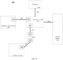
- FIG. 1A is a schematic block diagram of a system 100 that includes a transmitter and receiver coupled by a high speed data link in accordance with embodiments of the present disclosure.
- the transmitter 104 includes a waveform generator 106 that can output a waveform representative of data to be transmitted across the high speed data link 110.
- the transmitter 104 also includes a transmission (TX) buffer 108 for buffering data transmitted from the transmitter 104.
- the receiver 102 includes a neural network interpreter circuit 112.
- neural network (NN) circuit 112 which is referred to herein as an NN interpreter 112, is used to replace the EQ mechanism.
- the NN interpreter 112 takes the received voltage waveform as an input.
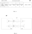
- FIG. 2 is an example graphical illustration of a waveform 200 illustrating sampling points 204 of the waveform and an example interested bit 202 in accordance with embodiments of the present disclosure.
- the interested bit 202 of waveform 200 is located in a unit interval spanning 15 and 20 UIs.
- the waveform can be sampled at 25 points using adjacent bits spanning UI 1-5, 6-10, 11-15, and 21-25, as well as sampling points at the interested bit between 16-20.
- the NN interpreter 112 can provide better performance than the EQ mechanism because the NN interpreter 112 determines each logic bit value from multiple samples in the input waveform, whereas the EQ mechanism relies on a slicer to sample the voltage at a single timing point for each bit. Compared to the traditional EQ mechanism, the NN interpreter is more immune to jitter, noise, and TX/RX nonlinearity, and thus can achieve much higher data rate.
- the activation layer of the NN interpreter 300 includes one or more activation layer circuit elements 308a-308n (H1-Hn) that each include two aspects: first, an activation function is applied to the input from the gain branches from each sampling point; second, the inputs, after the activation function is applied, as summed by a summer circuit element.
- An example activation function implemented using a hardware circuit element can include a CMOS very large scale integrated (VLSI) Hyperbolic Tangent Function circuit element. Other types of hardware implemented activation functions can also be used.
- the output of each activation layer element can be provided to a single output element 310, which sums the outputs by a summer circuit element.
- processor 500 is capable of executing a compiler, optimization, and/or translator code 577 to compile, translate, and/or optimize application code 576 to support the apparatus and methods described herein or to interface therewith.
- a compiler often includes a program or set of programs to translate source text/code into target text/code.
- compilation of program/application code with a compiler is done in multiple phases and passes to transform hi-level programming language code into low-level machine or assembly language code.
- single pass compilers may still be utilized for simple compilation.
- a compiler may utilize any known compilation techniques and perform any known compiler operations, such as lexical analysis, preprocessing, parsing, semantic analysis, code generation, code transformation, and code optimization.
- compiler code or dynamic optimization code may insert such operations/calls, as well as optimize the code for execution during runtime.
- binary code (already compiled code) may be dynamically optimized during runtime.
- the program code may include the dynamic optimization code, the binary code, or a combination thereof.
- PCI Express Peripheral Component Interconnect Express
- PCIe Peripheral Component Interconnect Express
- a primary goal of PCIe is to enable components and devices from different vendors to inter-operate in an open architecture, spanning multiple market segments; Clients (Desktops and Mobile), Servers (Standard and Enterprise), and Embedded and Communication devices.
- PCI Express is a high performance, general purpose I/O interconnect defined for a wide variety of future computing and communication platforms.
- Some PCI attributes, such as its usage model, load-store architecture, and software interfaces, have been maintained through its revisions, whereas previous parallel bus implementations have been replaced by a highly scalable, fully serial interface.
- PCI Express takes advantage of advances in point-to-point interconnects, Switch-based technology, and packetized protocol to deliver new levels of performance and features.
- Power Management Quality Of Service (QoS)
- Hot-Plug/Hot- Swap support Data Integrity, and Error Handling are among some of the advanced features supported by PCI Express.
- System 600 includes processor 605 and system memory 610 coupled to controller hub 615.
- Processor 605 includes any processing element, such as a microprocessor, a host processor, an embedded processor, a co-processor, or other processor.
- Processor 605 is coupled to controller hub 615 through front-side bus (FSB) 606.
- FSB 606 is a serial point-to-point interconnect as described below.
- link 606 includes a serial, differential interconnect architecture that is compliant with different interconnect standard.
- System memory 610 includes any memory device, such as random access memory (RAM), non-volatile (NV) memory, or other memory accessible by devices in system 600.
- System memory 610 is coupled to controller hub 615 through memory interface 616. Examples of a memory interface include a double-data rate (DDR) memory interface, a dual-channel DDR memory interface, and a dynamic RAM (DRAM) memory interface.
- DDR double-data rate
- DRAM dynamic RAM
- controller hub 615 is a root hub, root complex, or root controller in a Peripheral Component Interconnect Express (PCIe or PCIE) interconnection hierarchy.
- controller hub 615 include a chipset, a memory controller hub (MCH), a northbridge, an interconnect controller hub (ICH) a southbridge, and a root controller/hub.
- chipset refers to two physically separate controller hubs, i.e. a memory controller hub (MCH) coupled to an interconnect controller hub (ICH).
- MCH memory controller hub
- ICH interconnect controller hub
- current systems often include the MCH integrated with processor 605, while controller 615 is to communicate with I/O devices, in a similar manner as described below.
- peer-to-peer routing is optionally supported through root complex 615.
- controller hub 615 is coupled to switch/bridge 620 through serial link 619.
- Input/output modules 617 and 621 which may also be referred to as interfaces/ports 617 and 621, include/implement a layered protocol stack to provide communication between controller hub 615 and switch 620.
- multiple devices are capable of being coupled to switch 620.
- Switch/bridge 620 routes packets/messages from device 625 upstream, i.e. up a hierarchy towards a root complex, to controller hub 615 and downstream, i.e. down a hierarchy away from a root controller, from processor 605 or system memory 610 to device 625.
- Switch 620 in one embodiment, is referred to as a logical assembly of multiple virtual PCI-to-PCI bridge devices.
- Device 625 includes any internal or external device or component to be coupled to an electronic system, such as an I/O device, a Network Interface Controller (NIC), an add-in card, an audio processor, a network processor, a hard-drive, a storage device, a CD/DVD ROM, a monitor, a printer, a mouse, a keyboard, a router, a portable storage device, a Firewire device, a Universal Serial Bus (USB) device, a scanner, and other input/output devices.
- NIC Network Interface Controller
- an add-in card an audio processor
- a network processor a hard-drive
- a storage device a CD/DVD ROM
- monitor a printer
- printer printer
- mouse a keyboard
- USB Universal Serial Bus
- USB Universal Serial Bus
- scanner and other input/output devices.
- endpoint Often in the PCIe vernacular, such as device, is referred to as an endpoint.
- device 625 may include a PCIe to PCI/PCI-
- Graphics accelerator 630 is also coupled to controller hub 615 through serial link 632.
- graphics accelerator 630 is coupled to an MCH, which is coupled to an ICH.
- Switch 620, and accordingly I/O device 625, is then coupled to the ICH.
- I/O modules 631 and 618 are also to implement a layered protocol stack to communicate between graphics accelerator 630 and controller hub 615. Similar to the MCH discussion above, a graphics controller or the graphics accelerator 630 itself may be integrated in processor 605.
- Layered protocol stack 700 includes any form of a layered communication stack, such as a Quick Path Interconnect (QPI) stack, a PCie stack, a next generation high performance computing interconnect stack, or other layered stack.
- QPI Quick Path Interconnect
- PCie stack a next generation high performance computing interconnect stack
- protocol stack 700 is a PCIe protocol stack including transaction layer 705, link layer 710, and physical layer 720.
- An interface such as interfaces 617, 618, 621, 622, 626, and 631 in FIG. 6 , may be represented as communication protocol stack 700.
- Representation as a communication protocol stack may also be referred to as a module or interface implementing/including a protocol stack.
- PCI Express uses packets to communicate information between components. Packets are formed in the Transaction Layer 705 and Data Link Layer 710 to carry the information from the transmitting component to the receiving component. As the transmitted packets flow through the other layers, they are extended with additional information necessary to handle packets at those layers. At the receiving side the reverse process occurs and packets get transformed from their Physical Layer 720 representation to the Data Link Layer 710 representation and finally (for Transaction Layer Packets) to the form that can be processed by the Transaction Layer 705 of the receiving device.
- transaction layer 705 is to provide an interface between a device's processing core and the interconnect architecture, such as data link layer 710 and physical layer 720.
- a primary responsibility of the transaction layer 705 is the assembly and disassembly of packets (i.e., transaction layer packets, or TLPs).
- the translation layer 705 typically manages credit-base flow control for TLPs.
- PCIe implements split transactions, i.e. transactions with request and response separated by time, allowing a link to carry other traffic while the target device gathers data for the response.
- PCIe utilizes credit-based flow control.
- a device advertises an initial amount of credit for each of the receive buffers in Transaction Layer 705.
- An external device at the opposite end of the link such as controller hub 615 in FIG. 6 , counts the number of credits consumed by each TLP.
- a transaction may be transmitted if the transaction does not exceed a credit limit.
- Upon receiving a response an amount of credit is restored.
- An advantage of a credit scheme is that the latency of credit return does not affect performance, provided that the credit limit is not encountered.
- four transaction address spaces include a configuration address space, a memory address space, an input/output address space, and a message address space.
- Memory space transactions include one or more of read requests and write requests to transfer data to/from a memory-mapped location.
- memory space transactions are capable of using two different address formats, e.g., a short address format, such as a 32-bit address, or a long address format, such as 64-bit address.
- Configuration space transactions are used to access configuration space of the PCIe devices.
- Transactions to the configuration space include read requests and write requests.
- Message space transactions (or, simply messages) are defined to support in-band communication between PCIe agents.
- transaction layer 705 assembles packet header/payload 706. Format for current packet headers/payloads may be found in the PCIe specification at the PCIe specification website.
- transaction descriptor 800 is a mechanism for carrying transaction information.
- transaction descriptor 800 supports identification of transactions in a system.
- Other potential uses include tracking modifications of default transaction ordering and association of transaction with channels.
- Transaction descriptor 800 includes global identifier field 802, attributes field 804 and channel identifier field 806.
- global identifier field 802 is depicted comprising local transaction identifier field 808 and source identifier field 810.
- global transaction identifier 802 is unique for all outstanding requests.
- local transaction identifier field 808 is a field generated by a requesting agent, and it is unique for all outstanding requests that require a completion for that requesting agent. Furthermore, in this example, source identifier 810 uniquely identifies the requestor agent within a PCIe hierarchy. Accordingly, together with source ID 810, local transaction identifier 808 field provides global identification of a transaction within a hierarchy domain.
- Attributes field 804 specifies characteristics and relationships of the transaction. In this regard, attributes field 804 is potentially used to provide additional information that allows modification of the default handling of transactions.
- attributes field 804 includes priority field 812, reserved field 814, ordering field 816, and no-snoop field 818.
- priority sub-field 812 may be modified by an initiator to assign a priority to the transaction.
- Reserved attribute field 814 is left reserved for future, or vendor-defined usage. Possible usage models using priority or security attributes may be implemented using the reserved attribute field.
- Link layer 710 acts as an intermediate stage between transaction layer 705 and the physical layer 720.
- a responsibility of the data link layer 710 is providing a reliable mechanism for exchanging Transaction Layer Packets (TLPs) between two components a link.
- TLPs Transaction Layer Packets
- One side of the Data Link Layer 710 accepts TLPs assembled by the Transaction Layer 705, applies packet sequence identifier 711, i.e. an identification number or packet number, calculates and applies an error detection code, i.e. CRC 712, and submits the modified TLPs to the Physical Layer 720 for transmission across a physical to an external device.
- packet sequence identifier 711 i.e. an identification number or packet number
- CRC 712 error detection code
- physical layer 720 includes logical sub block 721 and electrical sub-block 722 to physically transmit a packet to an external device.
- logical sub-block 721 is responsible for the "digital" functions of Physical Layer 721.
- the logical sub-block includes a transmit section to prepare outgoing information for transmission by physical sub-block 722, and a receiver section to identify and prepare received information before passing it to the Link Layer 710.
- Physical block 722 includes a transmitter and a receiver.
- the transmitter is supplied by logical sub-block 721 with symbols, which the transmitter serializes and transmits onto to an external device.
- the receiver is supplied with serialized symbols from an external device and transforms the received signals into a bit-stream.
- the bit-stream is de-serialized and supplied to logical sub-block 721.
- an 8b/10b transmission code is employed, where ten-bit symbols are transmitted/received.
- special symbols are used to frame a packet with frames 723.
- the receiver also provides a symbol clock recovered from the incoming serial stream.
- a layered protocol stack is not so limited. In fact, any layered protocol may be included/implemented.
- an port/interface that is represented as a layered protocol includes: (1) a first layer to assemble packets, i.e. a transaction layer; a second layer to sequence packets, i.e. a link layer; and a third layer to transmit the packets, i.e. a physical layer.
- CSI common standard interface
- a serial point-to-point link is not so limited, as it includes any transmission path for transmitting serial data.
- a basic PCIe link includes two, low-voltage, differentially driven signal pairs: a transmit pair 906/911 and a receive pair 912/907.
- device 905 includes transmission logic 906 to transmit data to device 910 and receiving logic 907 to receive data from device 910.
- two transmitting paths i.e. paths 916 and 917
- two receiving paths i.e. paths 918 and 919
- a transmission path refers to any path for transmitting data, such as a transmission line, a copper line, an optical line, a wireless communication channel, an infrared communication link, or other communication path.
- a connection between two devices, such as device 905 and device 910, is referred to as a link, such as link 915.
- a link may support one lane - each lane representing a set of differential signal pairs (one pair for transmission, one pair for reception). To scale bandwidth, a link may aggregate multiple lanes denoted by xN, where N is any supported Link width, such as1, 2, 4, 8, 12, 16, 32, 64, or wider.
- a differential pair refers to two transmission paths, such as lines 916 and 917, to transmit differential signals.
- lines 916 and 917 to transmit differential signals.
- line 916 toggles from a low voltage level to a high voltage level, i.e. a rising edge
- line 917 drives from a high logic level to a low logic level, i.e. a falling edge.
- Differential signals potentially demonstrate better electrical characteristics, such as better signal integrity, i.e. cross-coupling, voltage overshoot/undershoot, ringing, etc. This allows for better timing window, which enables faster transmission frequencies.
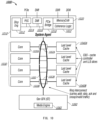
- processor 1000 includes multiple domains. Specifically, a core domain 1030 includes a plurality of cores 1030A-1030N, a graphics domain 1060 includes one or more graphics engines having a media engine 1065, and a system agent domain 1010.
- system agent domain 1010 handles power control events and power management, such that individual units of domains 1030 and 1060 (e.g. cores and/or graphics engines) are independently controllable to dynamically operate at an appropriate power mode/level (e.g. active, turbo, sleep, hibernate, deep sleep, or other Advanced Configuration Power Interface like state) in light of the activity (or inactivity) occurring in the given unit.
- an appropriate power mode/level e.g. active, turbo, sleep, hibernate, deep sleep, or other Advanced Configuration Power Interface like state
- Each of domains 1030 and 1060 may operate at different voltage and/or power, and furthermore the individual units within the domains each potentially operate at an independent frequency and voltage. Note that while only shown with three domains, understand the scope of the present disclosure is not limited in this regard and additional domains may be present in other embodiments.
- each core 1030 further includes low level caches in addition to various execution units and additional processing elements.
- the various cores are coupled to each other and to a shared cache memory that is formed of a plurality of units or slices of a last level cache (LLC) 1040A-1040N; these LLCs often include storage and cache controller functionality and are shared amongst the cores, as well as potentially among the graphics engine too.
- LLC last level cache
- a ring interconnect 1050 couples the cores together, and provides interconnection between the core domain 1030, graphics domain 1060 and system agent circuitry 1010, via a plurality of ring stops 1052A-1052N, each at a coupling between a core and LLC slice.
- interconnect 1050 is used to carry various information, including
- a design may go through various stages, from creation to simulation to fabrication.
- Data representing a design may represent the design in a number of manners.
- the hardware may be represented using a hardware description language or another functional description language.
- a circuit level model with logic and/or transistor gates may be produced at some stages of the design process.
- the data representing the hardware model may be the data specifying the presence or absence of various features on different mask layers for masks used to produce the integrated circuit.
- the data may be stored in any form of a machine readable medium.
- a memory or a magnetic or optical storage such as a disc may be the machine readable medium to store information transmitted via optical or electrical wave modulated or otherwise generated to transmit such information.
- an electrical carrier wave indicating or carrying the code or design is transmitted, to the extent that copying, buffering, or re-transmission of the electrical signal is performed, a new copy is made.
- a communication provider or a network provider may store on a tangible, machine-readable medium, at least temporarily, an article, such as information encoded into a carrier wave, embodying techniques of embodiments of the present disclosure.
- a module as used herein refers to any combination of hardware, software, and/or firmware.
- a module includes hardware, such as a micro-controller, associated with a non-transitory medium to store code adapted to be executed by the micro-controller. Therefore, reference to a module, in one embodiment, refers to the hardware, which is specifically configured to recognize and/or execute the code to be held on a non-transitory medium.
- use of a module refers to the non-transitory medium including the code, which is specifically adapted to be executed by the microcontroller to perform predetermined operations.
- the term module in this example may refer to the combination of the microcontroller and the non-transitory medium.
- a first and a second module may share hardware, software, firmware, or a combination thereof, while potentially retaining some independent hardware, software, or firmware.
- use of the term logic includes hardware, such as transistors, registers, or other hardware, such as programmable logic devices.
- phrase 'to' or 'configured to,' in one embodiment refers to arranging, putting together, manufacturing, offering to sell, importing and/or designing an apparatus, hardware, logic, or element to perform a designated or determined task.
- an apparatus or element thereof that is not operating is still 'configured to' perform a designated task if it is designed, coupled, and/or interconnected to perform said designated task.
- a logic gate may provide a 0 or a 1 during operation. But a logic gate 'configured to' provide an enable signal to a clock does not include every potential logic gate that may provide a 1 or 0.
- a non-transitory machine-accessible medium includes random-access memory (RAM), such as static RAM (SRAM) or dynamic RAM (DRAM); ROM; magnetic or optical storage medium; flash memory devices; electrical storage devices; optical storage devices; acoustical storage devices; other form of storage devices for holding information received from transitory (propagated) signals (e.g., carrier waves, infrared signals, digital signals); etc, which are to be distinguished from the non-transitory mediums that may receive information there from.
- RAM random-access memory
- SRAM static RAM
- DRAM dynamic RAM
- ROM magnetic or optical storage medium
- flash memory devices electrical storage devices
- optical storage devices e.g., optical storage devices
- acoustical storage devices other form of storage devices for holding information received from transitory (propagated) signals (e.g., carrier waves, infrared signals, digital signals); etc, which are to be distinguished from the non-transitory mediums that may receive information there from.
- a machine-readable medium may include any mechanism for storing or transmitting information in a form readable by a machine (e.g., a computer), but is not limited to, floppy diskettes, optical disks, Compact Disc, Read-Only Memory (CD-ROMs), and magnetooptical disks, Read-Only Memory (ROMs), Random Access Memory (RAM), Erasable Programmable Read-Only Memory (EPROM), Electrically Erasable Programmable Read-Only Memory (EEPROM), magnetic or optical cards, flash memory, or a tangible, machine-readable storage used in the transmission of information over the Internet via electrical, optical, acoustical or other forms of propagated signals (e.g., carrier waves, infrared signals, digital signals, etc.). Accordingly, the computer-readable signals
Landscapes
- Engineering & Computer Science (AREA)
- Artificial Intelligence (AREA)
- Evolutionary Computation (AREA)
- Power Engineering (AREA)
- Computer Networks & Wireless Communication (AREA)
- Signal Processing (AREA)
- Advance Control (AREA)
- Dc Digital Transmission (AREA)
Claims (7)
- Empfängereinrichtung, die konfiguriert ist zum Empfangen einer Datenwellenform (106) über eine Datenverbindung (110), wobei die Empfängereinrichtung (102) umfasst:
eine neuronale Netzwerkschaltung (112) zum:Empfangen einer Datenwellenform von der Datenverbindung; Abtasten der Datenwellenform zu einer Vielzahl von Zeitpunkten der Datenwellenform; undErmitteln eines Einzelbitwerts (114) für die Datenwellenform basierend auf dem Abtasten der Datenwellenform zu der Vielzahl von Zeitpunkten,wobei die neuronale Netzwerkschaltung eine Vielzahl von Verzögerungsschaltungen (302) umfasst, um die Datenwellenform zu verzögern, wobei die neuronale Netzwerkschaltung umfasst:eine erste Verzögerungsschaltung (302c), in Reihe geschaltet mit einer zweiten Verzögerungsschaltung (302b, 302a); wobei die neuronale Netzwerkschaltung ein erstes Abtastelement (304m) an einem Eingang zu der ersten Verzögerungsschaltung, ein zweites Abtastelement (304c) an einem Ausgang der ersten Verzögerungsschaltung und ein drittes Abtastelement (304b, 304a) an einem Ausgang der zweiten Verzögerungsschaltung umfasst; undwobei die Empfängereinrichtung ferner eine Vielzahl von Elementen einer Aktivierungsfunktionsschaltung (308) umfasst, um eine Aktivierungsfunktion auf einen oder mehrere Abtastwerte der Datenwellenform anzuwenden; und wobei die Empfängereinrichtung ferner eine Ausgangssummierschaltung (310) umfasst, wobei jedes aus der Vielzahl von Elementen einer Aktivierungsfunktionsschaltung mit der Ausgangssummierschaltung gekoppelt ist, wobei die Ausgangssummierschaltung geeignet ist, um die Ausgänge von jedem aus der Vielzahl von Elementen einer Aktivierungsfunktionsschaltung zu summieren, und geeignet ist, um den Einzelbitwert auszugeben, der ein interessierendes Bit aus der Datenwellenform repräsentiert. - Empfängereinrichtung nach Anspruch 1, die ferner ein Summierschaltungselement umfasst, das an einem Ausgang von jedem Element der Aktivierungsfunktionsschaltung untergebracht ist, wobei das Summierschaltungselement geeignet ist zum Summieren von jedem des einen oder der mehreren Abtastwerte der Datenwellenform, die der Anwendung der Aktivierungsfunktion unterzogen wurden.
- Empfängereinrichtung nach Anspruch 1, die ferner ein Verstärkungsschaltungselement (306) umfasst, die jeden Abtasteingang (304) mit jedem Aktivierungselement aus der Vielzahl von Aktivierungselementen verbindet, wobei das Verstärkungsschaltungselement konfiguriert ist zum Anwenden einer Verstärkung auf einen Abtastwert der Wellenform unter Verwendung eines oder mehrerer Verstärkungskoeffizienten.
- Verfahren zum Lösen eines Einzelbitwerts aus einer empfangenen Datenwellenform (106), wobei das Verfahren umfasst:Empfangen einer Datenwellenform in einem Element einer neuronalen Netzwerkschaltung (112);Abtasten der Datenwellenform an einem Zeitpunkt, der ein interessierendes Bit (202) repräsentiert;wobei das Verfahren ferner gekennzeichnet ist durchAbtasten der Datenwellenform an einem oder mehreren Zeitpunkten, die ein oder mehrere Bits in der Nähe des Zeitpunkts repräsentieren, der das interessierende Bit repräsentiert; undErmitteln des Einzelbitwerts (114) für das interessierende Bit, basierend auf dem Abtasten der Datenwellenform zu dem Zeitpunkt, der das interessierende Bit repräsentiert, und auf dem Abtasten der Datenwellenform zu dem einen oder den mehreren Zeitpunkten, die das eine oder die mehreren Bits in der Nähe des Zeitpunkts repräsentieren, der das interessierende Bit repräsentiert, wobei das Abtasten der Datenwellenform zu dem Zeitpunkt, der das interessierende Bit repräsentiert, und das Abtasten der Datenwellenform zu dem einen oder den mehreren Zeitpunkten, die das eine oder die mehreren Bits in der Nähe des Zeitpunkts repräsentieren, der das interessierende Bit repräsentiert, umfassen:Verzögern der Datenwellenform durch eine oder mehrere Verzögerungsschaltungen (302); undwobei das Abtasten der Datenwellenform zu einem Zeitpunkt, der ein interessierendes Bit repräsentiert, ein Abtasten der Datenwellenform zu mehreren Zeitpunkten im Verlauf eines Einheitsintervalls umfasst, das dem interessierenden Bit entspricht; undwobei das Abtasten der Datenwellenform zu dem einen oder den mehreren Zeitpunkten, die das eine oder die mehreren Bits in der Nähe des Zeitpunkts repräsentieren, der das interessierende Bit repräsentiert, ein Abtasten der Datenwellenform zu mehreren Zeitpunkten im Verlauf eines Einheitsintervalls umfasst, das jedem zu dem interessierenden Bit benachbarten Bit entspricht, wobei das Ermitteln des Einzelbitwerts für das interessierende Bit, basierend auf dem Abtasten der Datenwellenform zu dem Zeitpunkt, der das interessierende Bit repräsentiert, und auf dem Abtasten der Datenwellenform zu dem einen oder den mehreren Zeitpunkten, die das eine oder die mehreren Bits in der Nähe des Zeitpunkts repräsentieren, der das interessierende Bit repräsentiert, umfasst:Anwenden einer Aktivierungsfunktion (308) auf einen oder mehrere Abtastwerte der Datenwellenform von dem Zeitpunkt, der das interessierende Bit repräsentiert;Anwenden einer Aktivierungsfunktion (308) auf einen oder mehrere Abtastwerte der Datenwellenform von dem einen oder den mehreren Zeitpunkten, die ein oder mehrere Bits in der Nähe des Zeitpunkts repräsentieren, der das interessierende Bit repräsentiert; undSummieren der Abtastwerte der Datenwellenform nach dem Anwenden der Aktivierungsfunktionen; undwobei das Verfahren ferner ein Summieren (310) der summierten Abtastwerte und ein Ausgeben des Einzelbitwerts umfasst, der das interessierende Bit repräsentiert.
- Verfahren nach Anspruch 4, das ferner umfasst:Anwenden einer Verstärkung (306) auf einen oder mehrere Abtastwerte der Datenwellenform von dem Zeitpunkt, der das interessierende Bit repräsentiert, vor dem Anwenden der Aktivierungsfunktion; undAnwenden einer Verstärkung (306) auf einen oder mehrere Abtastwerte der Datenwellenform von dem einen oder den mehreren Zeitpunkten, die ein oder mehrere Bits in der Nähe des Zeitpunkts repräsentieren, der das interessierende Bit repräsentiert, nach dem Anwenden der Aktivierungsfunktion.
- Verfahren nach Anspruch 4, das ferner ein Trainieren einer Verstärkungsschaltung (306) zum Ermitteln eines Verstärkungskoeffizienten, um die Verstärkung auf einen oder mehrere Abtastwerte der Datenwellenform von dem Zeitpunkt an anzuwenden, der das interessierende Bit repräsentiert, und ein Trainieren einer Schaltung zum Ermitteln eines Verstärkungskoeffizienten umfasst, um eine Verstärkung auf einen oder mehrere Abtastwerte der Datenwellenform von dem einen oder den mehreren Zeitpunkten an anzuwenden, die ein oder mehrere Bits in der Nähe des Zeitpunkts repräsentieren, der das interessierende Bit repräsentiert, nach dem Anwenden der Aktivierungsfunktion.
- System, umfassend:einen Datensender (104) zum Senden einer Datenwellenform (106) ;einen Datenempfänger (103) zum Empfangen einer Datenwellenform von dem Datensender; undeine Datenverbindung (110), die den Datensender mit dem Datenempfänger koppelt;wobei der Datenempfänger umfasst:
eine neuronale Netzwerkschaltung (112) zum:Empfangen einer Datenwellenform von der Datenverbindung; wobei die neuronale Netzwerkschaltung ferner gekennzeichnet ist durchAbtasten der Datenwellenform zu einer Vielzahl von Zeitpunkten der Datenwellenform; undErmitteln eines Einzelbitwerts (114) für die Datenwellenform basierend auf dem Abtastwert der Wellenform von der Vielzahl von Zeitpunkten, wobei die neuronale Netzwerkschaltung eine Vielzahl von Verzögerungsschaltungen (302) umfasst, um die Datenwellenform zu verzögern, wobei die Vielzahl von Verzögerungsschaltungen umfasst:eine erste Verzögerungsschaltung (302c) in Reihe geschaltet mit einer zweiten Verzögerungsschaltung (302b, 302a);wobei die neuronale Netzwerkschaltung ein erstes Abtastelement (304m) an einem Eingang der ersten Verzögerungsschaltung, ein zweites Abtastelement (304c) an einem Ausgang der ersten Verzögerungsschaltung und ein drittes Abtastelement (304b, 304a) an einem Ausgang der zweiten Verzögerungsschaltung umfasst, wobei das System ferner eine Vielzahl von Elementen einer Aktivierungsfunktionsschaltung (308) umfasst, um eine Aktivierungsfunktion auf einen oder mehrere Abtastwerte der Datenwellenform anzuwenden; undwobei das System ferner eine Ausgangssummierschaltung (310) umfasst, wobei jedes aus der Vielzahl von Elementen einer Aktivierungsfunktionsschaltung mit der Ausgangssummierschaltung gekoppelt ist, wobei die Ausgangssummierschaltung geeignet ist, um die Ausgänge von jedem aus der Vielzahl von Elementen einer Aktivierungsfunktionsschaltung zu summieren, und geeignet ist, um den Einzelbitwert auszugeben, der ein interessierendes Bit aus der Datenwellenform repräsentiert.
Applications Claiming Priority (2)
| Application Number | Priority Date | Filing Date | Title |
|---|---|---|---|
| US15/446,277 US10084620B1 (en) | 2017-03-01 | 2017-03-01 | Neural network-based systems for high speed data links |
| PCT/US2018/019581 WO2018160465A1 (en) | 2017-03-01 | 2018-02-23 | Neural network-based systems for high speed data links |
Publications (3)
| Publication Number | Publication Date |
|---|---|
| EP3590239A1 EP3590239A1 (de) | 2020-01-08 |
| EP3590239A4 EP3590239A4 (de) | 2021-01-06 |
| EP3590239B1 true EP3590239B1 (de) | 2025-07-02 |
Family
ID=63355922
Family Applications (1)
| Application Number | Title | Priority Date | Filing Date |
|---|---|---|---|
| EP18761068.8A Active EP3590239B1 (de) | 2017-03-01 | 2018-02-23 | Auf neuronalem netzwerk basierte systeme für hochgeschwindigkeitsdatenverbindungen |
Country Status (3)
| Country | Link |
|---|---|
| US (1) | US10084620B1 (de) |
| EP (1) | EP3590239B1 (de) |
| WO (1) | WO2018160465A1 (de) |
Families Citing this family (3)
| Publication number | Priority date | Publication date | Assignee | Title |
|---|---|---|---|---|
| CN109922427B (zh) * | 2019-03-06 | 2020-09-11 | 东南大学 | 利用大规模阵列天线的智能无线定位系统和方法 |
| US11483123B2 (en) * | 2019-09-13 | 2022-10-25 | Nokomis, Inc | Direct conversion receiver using coherent integration |
| US12224756B2 (en) * | 2022-07-04 | 2025-02-11 | Mediatek Inc. | Clock and data recovery circuit using neural network circuit to obtain frequency difference information |
Citations (1)
| Publication number | Priority date | Publication date | Assignee | Title |
|---|---|---|---|---|
| EP0498574B1 (de) * | 1991-01-31 | 1997-07-23 | Victor Company Of Japan, Limited | Einrichtung zur Wellenformentzerrung mit neuronalem Netzwerk und Verfahren zum Entwurf derselben |
Family Cites Families (11)
| Publication number | Priority date | Publication date | Assignee | Title |
|---|---|---|---|---|
| US4906865A (en) | 1988-12-09 | 1990-03-06 | Intel Corporation | Sample and hold circuit for temporal associations in a neural network |
| JPH0369238A (ja) * | 1989-08-08 | 1991-03-25 | Mitsubishi Electric Corp | 復調データ識別判定装置 |
| EP0454445B1 (de) * | 1990-04-26 | 1996-07-03 | Fujitsu Limited | Wellenformentzerrer mit Neuronalnetzwerk |
| DE4415811A1 (de) * | 1994-05-05 | 1995-11-09 | Thomson Brandt Gmbh | Verfahren zum Entzerren von verzerrten Datensignalen |
| JPH10106158A (ja) | 1996-09-30 | 1998-04-24 | Toshiba Corp | ディスク記憶装置及び同装置に適用する波形等化回路 |
| US7991099B2 (en) * | 2008-04-02 | 2011-08-02 | Lontium Semiconductor Corp. | Clock and/or data recovery |
| US10742953B2 (en) * | 2009-01-20 | 2020-08-11 | Koninklijke Philips N.V. | Transferring of three-dimensional image data |
| JP4840494B2 (ja) | 2009-09-16 | 2011-12-21 | 沖電気工業株式会社 | 時系列データ予測ニューラルネットワーク装置 |
| US8265133B2 (en) * | 2009-09-30 | 2012-09-11 | Silicon Laboratories Inc. | Radio receiver having a multipath equalizer |
| US9536190B2 (en) | 2013-10-17 | 2017-01-03 | Qualcomm Incorporated | Dynamically assigning and examining synaptic delay |
| US20160328642A1 (en) | 2015-05-06 | 2016-11-10 | Indiana University Research And Technology Corporation | Sensor signal processing using an analog neural network |
-
2017
- 2017-03-01 US US15/446,277 patent/US10084620B1/en not_active Expired - Fee Related
-
2018
- 2018-02-23 WO PCT/US2018/019581 patent/WO2018160465A1/en not_active Ceased
- 2018-02-23 EP EP18761068.8A patent/EP3590239B1/de active Active
Patent Citations (1)
| Publication number | Priority date | Publication date | Assignee | Title |
|---|---|---|---|---|
| EP0498574B1 (de) * | 1991-01-31 | 1997-07-23 | Victor Company Of Japan, Limited | Einrichtung zur Wellenformentzerrung mit neuronalem Netzwerk und Verfahren zum Entwurf derselben |
Also Published As
| Publication number | Publication date |
|---|---|
| EP3590239A1 (de) | 2020-01-08 |
| US10084620B1 (en) | 2018-09-25 |
| WO2018160465A1 (en) | 2018-09-07 |
| US20180254928A1 (en) | 2018-09-06 |
| EP3590239A4 (de) | 2021-01-06 |
Similar Documents
| Publication | Publication Date | Title |
|---|---|---|
| US11573920B2 (en) | SERDES link training | |
| US10963415B2 (en) | Bimodal PHY for low latency in high speed interconnects | |
| EP2779517B1 (de) | Vorrichtung, System, und Verfahren zur Verbesserung der Entzerrung mit einem hardwareangetriebenen Algorithmus | |
| US11153032B2 (en) | Forward error correction mechanism for peripheral component interconnect-express (PCI-E) | |
| EP2778938B1 (de) | Vorrichtung, System und Verfahren zur Durchführung von Link-Training und -Ausgleich | |
| US11593280B2 (en) | Predictive packet header compression | |
| US20220414046A1 (en) | Systems, methods, and devices for dynamic high speed lane direction switching for asymmetrical interfaces | |
| US12316446B2 (en) | Latency optimization in partial width link states | |
| US10250436B2 (en) | Applying framing rules for a high speed data link | |
| US11016920B2 (en) | Adaptive calibration technique for cross talk cancellation | |
| US10846258B2 (en) | Voltage modulated control lane | |
| EP3590239B1 (de) | Auf neuronalem netzwerk basierte systeme für hochgeschwindigkeitsdatenverbindungen | |
| US9575922B2 (en) | Apparatus, system, and method for improving equalization with a software equalization algorithm | |
| US8958471B2 (en) | Method, apparatus, and system for sliding matrix scoreboard utilized in auto feedback closed loops |
Legal Events
| Date | Code | Title | Description |
|---|---|---|---|
| STAA | Information on the status of an ep patent application or granted ep patent |
Free format text: STATUS: THE INTERNATIONAL PUBLICATION HAS BEEN MADE |
|
| PUAI | Public reference made under article 153(3) epc to a published international application that has entered the european phase |
Free format text: ORIGINAL CODE: 0009012 |
|
| STAA | Information on the status of an ep patent application or granted ep patent |
Free format text: STATUS: REQUEST FOR EXAMINATION WAS MADE |
|
| 17P | Request for examination filed |
Effective date: 20190625 |
|
| AK | Designated contracting states |
Kind code of ref document: A1 Designated state(s): AL AT BE BG CH CY CZ DE DK EE ES FI FR GB GR HR HU IE IS IT LI LT LU LV MC MK MT NL NO PL PT RO RS SE SI SK SM TR |
|
| AX | Request for extension of the european patent |
Extension state: BA ME |
|
| RIN1 | Information on inventor provided before grant (corrected) |
Inventor name: CHEN, FAN Inventor name: PHARES, CHARLES Inventor name: LANG, JOHN Inventor name: CHU, YUNHUI |
|
| DAV | Request for validation of the european patent (deleted) | ||
| DAX | Request for extension of the european patent (deleted) | ||
| REG | Reference to a national code |
Ref country code: DE Ref legal event code: R079 Free format text: PREVIOUS MAIN CLASS: H04L0025020000 Ipc: H04L0025030000 |
|
| A4 | Supplementary search report drawn up and despatched |
Effective date: 20201204 |
|
| RIC1 | Information provided on ipc code assigned before grant |
Ipc: H04L 25/03 20060101AFI20201130BHEP |
|
| STAA | Information on the status of an ep patent application or granted ep patent |
Free format text: STATUS: EXAMINATION IS IN PROGRESS |
|
| 17Q | First examination report despatched |
Effective date: 20221116 |
|
| GRAP | Despatch of communication of intention to grant a patent |
Free format text: ORIGINAL CODE: EPIDOSNIGR1 |
|
| STAA | Information on the status of an ep patent application or granted ep patent |
Free format text: STATUS: GRANT OF PATENT IS INTENDED |
|
| INTG | Intention to grant announced |
Effective date: 20240917 |
|
| GRAJ | Information related to disapproval of communication of intention to grant by the applicant or resumption of examination proceedings by the epo deleted |
Free format text: ORIGINAL CODE: EPIDOSDIGR1 |
|
| STAA | Information on the status of an ep patent application or granted ep patent |
Free format text: STATUS: EXAMINATION IS IN PROGRESS |
|
| GRAP | Despatch of communication of intention to grant a patent |
Free format text: ORIGINAL CODE: EPIDOSNIGR1 |
|
| STAA | Information on the status of an ep patent application or granted ep patent |
Free format text: STATUS: GRANT OF PATENT IS INTENDED |
|
| INTC | Intention to grant announced (deleted) | ||
| INTG | Intention to grant announced |
Effective date: 20250128 |
|
| GRAS | Grant fee paid |
Free format text: ORIGINAL CODE: EPIDOSNIGR3 |
|
| GRAA | (expected) grant |
Free format text: ORIGINAL CODE: 0009210 |
|
| STAA | Information on the status of an ep patent application or granted ep patent |
Free format text: STATUS: THE PATENT HAS BEEN GRANTED |
|
| AK | Designated contracting states |
Kind code of ref document: B1 Designated state(s): AL AT BE BG CH CY CZ DE DK EE ES FI FR GB GR HR HU IE IS IT LI LT LU LV MC MK MT NL NO PL PT RO RS SE SI SK SM TR |
|
| REG | Reference to a national code |
Ref country code: GB Ref legal event code: FG4D |
|
| REG | Reference to a national code |
Ref country code: CH Ref legal event code: EP |
|
| REG | Reference to a national code |
Ref country code: DE Ref legal event code: R096 Ref document number: 602018083202 Country of ref document: DE |
|
| P01 | Opt-out of the competence of the unified patent court (upc) registered |
Free format text: CASE NUMBER: APP_28478/2025 Effective date: 20250615 |
|
| REG | Reference to a national code |
Ref country code: IE Ref legal event code: FG4D |
|
| REG | Reference to a national code |
Ref country code: NL Ref legal event code: FP |
|
| PG25 | Lapsed in a contracting state [announced via postgrant information from national office to epo] |
Ref country code: PT Free format text: LAPSE BECAUSE OF FAILURE TO SUBMIT A TRANSLATION OF THE DESCRIPTION OR TO PAY THE FEE WITHIN THE PRESCRIBED TIME-LIMIT Effective date: 20251103 |
|
| REG | Reference to a national code |
Ref country code: AT Ref legal event code: MK05 Ref document number: 1810560 Country of ref document: AT Kind code of ref document: T Effective date: 20250702 |
|
| PG25 | Lapsed in a contracting state [announced via postgrant information from national office to epo] |
Ref country code: IS Free format text: LAPSE BECAUSE OF FAILURE TO SUBMIT A TRANSLATION OF THE DESCRIPTION OR TO PAY THE FEE WITHIN THE PRESCRIBED TIME-LIMIT Effective date: 20251102 |
|
| PG25 | Lapsed in a contracting state [announced via postgrant information from national office to epo] |
Ref country code: NO Free format text: LAPSE BECAUSE OF FAILURE TO SUBMIT A TRANSLATION OF THE DESCRIPTION OR TO PAY THE FEE WITHIN THE PRESCRIBED TIME-LIMIT Effective date: 20251002 |
|
| REG | Reference to a national code |
Ref country code: LT Ref legal event code: MG9D |
|
| PG25 | Lapsed in a contracting state [announced via postgrant information from national office to epo] |
Ref country code: AT Free format text: LAPSE BECAUSE OF FAILURE TO SUBMIT A TRANSLATION OF THE DESCRIPTION OR TO PAY THE FEE WITHIN THE PRESCRIBED TIME-LIMIT Effective date: 20250702 |
|
| PG25 | Lapsed in a contracting state [announced via postgrant information from national office to epo] |
Ref country code: FI Free format text: LAPSE BECAUSE OF FAILURE TO SUBMIT A TRANSLATION OF THE DESCRIPTION OR TO PAY THE FEE WITHIN THE PRESCRIBED TIME-LIMIT Effective date: 20250702 |
|
| PG25 | Lapsed in a contracting state [announced via postgrant information from national office to epo] |
Ref country code: HR Free format text: LAPSE BECAUSE OF FAILURE TO SUBMIT A TRANSLATION OF THE DESCRIPTION OR TO PAY THE FEE WITHIN THE PRESCRIBED TIME-LIMIT Effective date: 20250702 |
|
| PG25 | Lapsed in a contracting state [announced via postgrant information from national office to epo] |
Ref country code: GR Free format text: LAPSE BECAUSE OF FAILURE TO SUBMIT A TRANSLATION OF THE DESCRIPTION OR TO PAY THE FEE WITHIN THE PRESCRIBED TIME-LIMIT Effective date: 20251003 |
|
| PG25 | Lapsed in a contracting state [announced via postgrant information from national office to epo] |
Ref country code: SE Free format text: LAPSE BECAUSE OF FAILURE TO SUBMIT A TRANSLATION OF THE DESCRIPTION OR TO PAY THE FEE WITHIN THE PRESCRIBED TIME-LIMIT Effective date: 20250702 Ref country code: CZ Free format text: LAPSE BECAUSE OF FAILURE TO SUBMIT A TRANSLATION OF THE DESCRIPTION OR TO PAY THE FEE WITHIN THE PRESCRIBED TIME-LIMIT Effective date: 20250702 |
|
| PG25 | Lapsed in a contracting state [announced via postgrant information from national office to epo] |
Ref country code: LV Free format text: LAPSE BECAUSE OF FAILURE TO SUBMIT A TRANSLATION OF THE DESCRIPTION OR TO PAY THE FEE WITHIN THE PRESCRIBED TIME-LIMIT Effective date: 20250702 |
|
| PG25 | Lapsed in a contracting state [announced via postgrant information from national office to epo] |
Ref country code: BG Free format text: LAPSE BECAUSE OF FAILURE TO SUBMIT A TRANSLATION OF THE DESCRIPTION OR TO PAY THE FEE WITHIN THE PRESCRIBED TIME-LIMIT Effective date: 20250702 Ref country code: PL Free format text: LAPSE BECAUSE OF FAILURE TO SUBMIT A TRANSLATION OF THE DESCRIPTION OR TO PAY THE FEE WITHIN THE PRESCRIBED TIME-LIMIT Effective date: 20250702 |
|
| PG25 | Lapsed in a contracting state [announced via postgrant information from national office to epo] |
Ref country code: RS Free format text: LAPSE BECAUSE OF FAILURE TO SUBMIT A TRANSLATION OF THE DESCRIPTION OR TO PAY THE FEE WITHIN THE PRESCRIBED TIME-LIMIT Effective date: 20251002 |
|
| PG25 | Lapsed in a contracting state [announced via postgrant information from national office to epo] |
Ref country code: ES Free format text: LAPSE BECAUSE OF FAILURE TO SUBMIT A TRANSLATION OF THE DESCRIPTION OR TO PAY THE FEE WITHIN THE PRESCRIBED TIME-LIMIT Effective date: 20250702 |