EP3586239B1 - Multiidentitäts-optikmodule - Google Patents
Multiidentitäts-optikmodule Download PDFInfo
- Publication number
- EP3586239B1 EP3586239B1 EP18708550.1A EP18708550A EP3586239B1 EP 3586239 B1 EP3586239 B1 EP 3586239B1 EP 18708550 A EP18708550 A EP 18708550A EP 3586239 B1 EP3586239 B1 EP 3586239B1
- Authority
- EP
- European Patent Office
- Prior art keywords
- data rate
- host
- module
- identity
- optics module
- Prior art date
- Legal status (The legal status is an assumption and is not a legal conclusion. Google has not performed a legal analysis and makes no representation as to the accuracy of the status listed.)
- Active
Links
Images





Classifications
-
- H—ELECTRICITY
- H04—ELECTRIC COMMUNICATION TECHNIQUE
- H04B—TRANSMISSION
- H04B10/00—Transmission systems employing electromagnetic waves other than radio-waves, e.g. infrared, visible or ultraviolet light, or employing corpuscular radiation, e.g. quantum communication
- H04B10/07—Arrangements for monitoring or testing transmission systems; Arrangements for fault measurement of transmission systems
- H04B10/075—Arrangements for monitoring or testing transmission systems; Arrangements for fault measurement of transmission systems using an in-service signal
- H04B10/077—Arrangements for monitoring or testing transmission systems; Arrangements for fault measurement of transmission systems using an in-service signal using a supervisory or additional signal
- H04B10/0775—Performance monitoring and measurement of transmission parameters
-
- G—PHYSICS
- G02—OPTICS
- G02B—OPTICAL ELEMENTS, SYSTEMS OR APPARATUS
- G02B6/00—Light guides; Structural details of arrangements comprising light guides and other optical elements, e.g. couplings
- G02B6/24—Coupling light guides
- G02B6/42—Coupling light guides with opto-electronic elements
- G02B6/4201—Packages, e.g. shape, construction, internal or external details
- G02B6/4274—Electrical aspects
- G02B6/4278—Electrical aspects related to pluggable or demountable opto-electronic or electronic elements
-
- G—PHYSICS
- G06—COMPUTING OR CALCULATING; COUNTING
- G06F—ELECTRIC DIGITAL DATA PROCESSING
- G06F13/00—Interconnection of, or transfer of information or other signals between, memories, input/output devices or central processing units
- G06F13/38—Information transfer, e.g. on bus
- G06F13/382—Information transfer, e.g. on bus using universal interface adapter
- G06F13/385—Information transfer, e.g. on bus using universal interface adapter for adaptation of a particular data processing system to different peripheral devices
-
- H—ELECTRICITY
- H04—ELECTRIC COMMUNICATION TECHNIQUE
- H04B—TRANSMISSION
- H04B10/00—Transmission systems employing electromagnetic waves other than radio-waves, e.g. infrared, visible or ultraviolet light, or employing corpuscular radiation, e.g. quantum communication
- H04B10/25—Arrangements specific to fibre transmission
- H04B10/2581—Multimode transmission
-
- H—ELECTRICITY
- H04—ELECTRIC COMMUNICATION TECHNIQUE
- H04B—TRANSMISSION
- H04B10/00—Transmission systems employing electromagnetic waves other than radio-waves, e.g. infrared, visible or ultraviolet light, or employing corpuscular radiation, e.g. quantum communication
- H04B10/40—Transceivers
Definitions
- the present disclosure relates to multi-identity multi-rate optics modules.
- US 2005/0111845 A is disclosing a controller receiving a rate select signal that indicates a set of operational data rates for the optical transmitter.
- Optics modules are compact transceivers often used in data centers.
- Optics modules typically interface a host module (e.g., host card) with a fiber optic cable, and are generally designed to support one or more specific data rates (e.g., 1, 2.5, 10, 25, 50, etc. Gbit/s (G)) corresponding to a given platform.
- G Gbit/s
- single-rate 10G optics modules are generally compatible with single-rate 10G host modules.
- single-rate 10G optics modules are not compatible with single-rate 25G host modules, and single-rate 25G optics modules are not compatible with single-rate 10G host modules.
- conventional multi-rate optics modules are only compatible with host modules having the host module software driver support for proper optics recognition.
- dual-rate 10/25G optics modules are generally compatible with dual-rate 10/25G host modules but not with single-rate 25G platforms because single-rate 25G host modules lack the requisite host module software driver support.
- current multi-rate optics modules are not generally compatible with their corresponding single-rate host modules.
- an optics module sends, to a host module, a pin signal indicating that an optics module is plugged into the host module, wherein the optics module is configured to operate at at least a first data rate and a second data rate.
- the optics module receives, from the host module, an indication of a host data rate.
- the optics module determines whether there is clock and data recovery loss of lock between the first data rate and a host data rate. If it is determined that there is clock and data recovery loss of lock between the first data rate and the host data rate, the optics module initializes at the second data rate.
- a multi-identity multi-rate optics (optical) module that is generally compatible with its associated single-rate host module without requiring a software driver change on the single-rate host module.
- a multi-identity dual-rate 10/25G optics module is generally compatible with single-rate 10G host modules, single-rate 25G host modules, and dual-rate 10/25G host modules.
- a multi-identity tri-rate 10/25/50G optics module is generally compatible with single-rate 10G host modules, single-rate 25G host modules, dual-rate (e.g., 10/25G) host modules, tri-rate (e.g., 10/25/50G) host modules, etc.
- the node is an optical network node that includes host cards 110(1)-110(3), multi-identity optics modules 115(1)-115(3), and fiber optic cables 120(1)-120(3).
- Fiber optic cables 120(1)-120(3) transport optical signals that carry data between the node 100 and the network 105 at different rates.
- fiber optic cables 120(1) and 120(3) transport optical signals at a transmit data at a rate of 10G
- fiber optic cable 120(2) transports optical signals at a transmit data at a rate of 25G.
- Host cards 110(1)-110(3) are respectively configured to handle the data rates of fiber optic cables 120(1)-120(3).
- host card 110(1) is a single-rate (e.g., 10G) host module
- host card 110(2) is a single-rate (e.g., 25G) host module
- host card 110(3) is a dual-rate (e.g., 10/25G) host module. Because host card 110(3) is dual-rate, it is compatible with either 10G or 25G data rates.
- Fiber optic cables 120(1)-120(3) carry data in the form of optical signals, but host cards 110(1)-110(3) are configured to handle electrical signals.
- multi-identity optics modules 115(1)-115(3) are provided to interface the host cards 110(1)-110(3) and fiber optic cables 120(1)-120(3).
- multi-identity optics module 115(1) converts incoming optical signals from fiber optic cable 120(1) to electrical signals for host card 110(1).
- Multi-identity optics module 115(1) also converts incoming electrical signals from host card 110(1) to optical signals for fiber optic cable 120(1).
- multi-identity optics modules 115(1)-115(3) are each of the same type (e.g., multi-identity dual-rate 10/25G optics modules).
- multi-identity optics modules 115(1)-115(3) are generally compatible with host card 110(1) (e.g., 10G), host card 110(2) (e.g., 25G), and host card 110(3) (e.g., 10/25G).
- sequence diagrams 200A and 200B illustrating communication between a host module and a multi-identity optics module in accordance with examples presented herein.
- a user inserts the multi-identity optics module into the host module.
- the multi-identity optics module negates a module absent (MOD_ABS) signal.
- MOD_ABS indicates the absence of the multi-identity optics module.
- the host module detects the presence of the multi-identity optics module at 215.
- the host module begins reading an electrically erasable programmable read-only memory (EEPROM) map from a memory buffer of the multi-identity optics module that is accessible by the host module.
- the EEPROM map specifies a data rate at which the multi-identity optics module is currently configured to operate.
- the multi-identity optics module includes multiple EEPROM maps, each corresponding to a different data rate.
- the multi-identity optics module sends the content of the EEPROM map to the host module until the host module has completely read the EEPROM map at 230.
- the host module determines that the content of the EEPROM map (e.g., the specified data rate) matches with a library storing an indication of the data rate of the host module.
- the host module sends an idle character to the multi-identity optics module at 240.
- the multi-identity optics module determines whether there is clock and data recovery loss of lock between the multi-identity optics module data rate and the host data rate. Clock and data recovery enables the multi-identity optics module to sample the idle character to determine the host module data rate.
- the multi-identity optics module determines that there is no clock and data recovery loss of lock between the multi-identity optics module data rate and the host data rate. In other words, the multi-identity optics module and the host data rates lock/match.
- the host module is a single-rate 25G host card and the EEPROM map specifies that the multi-identity optics module is currently configured to operate at a data rate of 25G.
- the host module determines that the rate specified in the EEPROM map (25G) matches the host data rate (also 25G).
- multi-identity optics module determines from the idle character that the host data rate (25G) matches the rate specified in the EEPROM map (also 25G).
- the host module determines the data rate at which the multi-identity optics module is currently configured to operate based on the EEPROM map.
- the multi-identity optics module determines the host data rate based on the idle character. As such, at 255, the host module links up with the multi-identity module, and at 260 the multi-identity optics module boots as normal.
- FIG. 2B is a sequence diagram 200B illustrating communication between a host module and a multi-identity optics module in accordance with examples presented herein.
- Sequence diagram 200B is similar to sequence diagram 200A. However, whereas the sequence in FIG. 2A involves the host module reading the EEPROM map before sending the idle character to module, the sequence in FIG. 2B involves the host reading the EEPROM map after sending idle character to module.
- the multi-identity optics module is inserted (e.g., by a user).
- the multi-identity optics module negates the MOD_ABS signal.
- the host module detects the presence of the multi-identity optics module.
- the host module begins reading the EEPROM map.
- the multi-identity optics module sends the content of the EEPROM map to the host module. In the example sequence of FIG. 2B , the host module sends the idle character at 240 before the host module has completely read the EEPROM map at 230.
- the multi-identity optics module determines that there is no clock and data recovery loss of lock between the multi-identity optics module data rate and the host data rate at 245 and 250 while the host is reading the EEPROM map.
- the host module determines that the content of the EEPROM map (e.g., the specified data rate) matches a library storing an indication of the data rate of the host module.
- the host module links up with the multi-identity module, and at 255 the multi-identity optics module boots as normal.
- FIG. 3 is a sequence diagram illustrating communication between a host module and a multi-identity optics module in accordance with another example embodiment.
- the sequence of FIG. 3 involves a 10G host module and a dual-rate 10/25G multi-identity optics module.
- the host module sends the idle character before the host module has completely read the EEPROM map.
- this sequence involves a mismatch between the first EEPROM map that the host module reads and the host module data rate.
- the multi-identity optics module is inserted (e.g., by a user).
- the multi-identity optics module negates the MOD_ABS signal.
- the host module detects the presence of the multi-identity optics module.
- the host module begins reading a first EEPROM map.
- the first EEPROM map specifies a multi-identity optics module data rate of 25G.
- the multi-identity optics module sends the content of the first EEPROM map to the host module.
- the host module sends the idle character to the multi-identity optics module.
- the multi-identity optics module determines whether there is clock and data recovery loss of lock between the current multi-identity optics module data rate (i.e., 25G) and the host data rate.
- the multi-identity optics module determines that there is clock and data recovery loss of lock between the current multi-identity optics module data rate and the host data rate. From the perspective of the multi-identity optics module, this is because the data rate of the host device (as indicated by the idle character) is 10G, whereas the current multi-identity optics module data rate (as specified by the first EEPROM map) is 25G.
- the host module finishes reading the EEPROM map and determines that the content of the EEPROM map (e.g., the specified data rate) does not match a library storing an indication of the data rate of the host module. From the perspective of the host module, this is because the data rate of the host module (as indicated in the library) is 10G, whereas the current multi-identity optics module data rate is 25G (as specified by the first EEPROM map). Accordingly, the host module keeps the link down at 322.
- the content of the EEPROM map e.g., the specified data rate
- the multi-identity optics module determines at 316 that there was clock and data recovery loss of lock between the 25G multi-identity optics module data rate and the 10G host data rate, the multi-identity optics module sets the rate in a non-volatile random access memory (NVRAM) to 10G at 324.
- the multi-identity optics module asserts a MOD_ABS signal to the host module to indicate the absence of the multi-identity optics module.
- the host receives the MOD_ABS signal at 328 and, in response, removes the multi-identity optics module at 330.
- the multi-identity optics module asserts a MOD_ABS signal and, at 332, waits for approximately one second.
- the multi-identity optics module negates a MOD_ABS signal.
- the host module receives the signal negating MOD_ABS, causing the host module to detect the presence of the multi-identity optics module at 338.
- the host module begins reading the second EEPROM map, which specifies a multi-identity optics module data rate of 10G.
- the multi-identity optics module sends the content of the second EEPROM map to the host module.
- the host module sends the idle character to the multi-identity optics module.
- the multi-identity optics module determines whether there is clock and data recovery loss of lock between the current multi-identity optics module data rate (i.e., 10G) and the host data rate.
- the multi-identity optics module determines that there is no clock and data recovery loss of lock between the current multi-identity optics module data rate and the host data rate.
- the multi-identity optics module boots as normal at 350.
- the host module finishes reading the EEPROM map and determines that the content of the EEPROM map (e.g., the specified data rate) matches the library storing the indication of the data rate of the host module. From the perspective of the host module, this is because the data rate of the host module (as indicated in the library) and the current multi-identity optics module data rate (as specified by the first EEPROM map) are both 10G. Accordingly, at 356, the host module links up with the multi-identity optics module.
- the content of the EEPROM map e.g., the specified data rate
- FIG. 4 is a high-level flowchart 400 of a method for initializing a multi-identity optics module at a host module.
- the presence of the multi-identity optics module is asserted.
- the flow proceeds to 420, where the multi-identity optics module data rate sets an alternate EEPROM map that specifies an alternate multi-identity optics module data rate.
- the multi-identity optics module asserts a "break-and-make" presence signal.
- a purpose of the "break-and-make” presence signal is to provoke the host module to read the alternate EEPROM map.
- the "break-and-make" presence signal may involve asserting a MOD_ABS signal and then negating the MOD_ABS signal after some time.
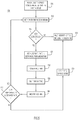
- FIG. 5 is a flowchart 500 of an example method for initializing a dual-rate (e.g., 10/25G) multi-identity optics module on a 10G host module.
- the 10/25G multi-identity optics module includes a NVRAM and two EEPROM maps respectively specifying multi-identity optics module data rates (i.e., 10G and 25G).
- the multi-identity optics module is inserted into the host module.
- the multi-identity optics module sets the clock and data recovery rate to the rate currently stored in the NVRAM.
- 25G is the default rate (i.e., the data rate initially stored in the NVRAM).
- the multi-identity optics module 25G data rate is also stored in an EEPROM buffer to allow the host module to read the 25G EEPROM content.
- the multi-identity optics module determines whether there is clock and data recovery loss of lock between the current multi-identity optics module data rate (i.e., 25G) and the host data rate (i.e., 10G). If there is no clock and data recovery loss of lock ("No"), the multi-identity optics module initializes at 520. However, in this example there is clock and data recovery loss of lock ("Yes") because the current multi-identity optics module data rate (i.e., 25G) is different from the host data rate (i.e., 10G). As such, the flow proceeds to 525, at which the multi-identity optics module sets the alternate rate (i.e., 10G) in the EEPROM buffer and NVRAM.
- the multi-identity optics module asserts a "break-and-make" presence signal.
- the multi-identity optics module asserts a MOD_ABS signal to indicate the absence of the multi-identity optics module to the host module.
- the multi-identity optics module waits for a period of time (e.g., one second).
- the multi-identity optics module negates the MOD_ABS signal. This causes the host module to recognize the multi-identity optics module.
- the "break-and-make" presence signal enables the multi-identity optics module to remain plugged in to the host module while setting the alternate data rate.
- a 25G optics module was inserted (505), the 25G optics module was physically removed (530), and a 10G optics module was inserted (540).
- the multi-identity module remained inserted in the host module and while providing both 10G and 25G data rates.
- the multi-identity optics module supports clock and data recovery at 25G
- the multi-identity optics module may or may not support clock and data recovery at 10G.
- the multi-identity optics module determines whether the multi-identity optics module supports clock and data recovery at the 10G data rate. If the multi-identity optics module does not support clock and data recovery at the 10G data rate ("No"), the multi-identity optics module sets the clock and data recovery to bypass mode. This enables the multi-identity optics module to initialize at 520 without determining whether there is clock and data recovery loss of lock.
- the multi-identity optics module If the multi-identity optics module supports clock and data recovery at the 10G data rate ("Yes"), the multi-identity optics module sets the clock and data recovery rate to the rate in the NVRAM at 510. Per 525, the rate in the NVRAM is 10G. At 515, the multi-identity optics module determines whether there is clock and data recovery loss of lock between the current multi-identity optics module data rate (i.e., 10G) and the host data rate (i.e., 10G). Because these rates match, there is no clock and data recovery loss of lock (“No"), and the multi-identity optics module initializes at 520.
- the current multi-identity optics module data rate i.e., 10G
- the host data rate i.e. 10G
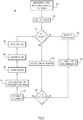
- FIG. 6 is a flowchart 600 of an example method for initializing a tri-rate (e.g., 10/25/50G) multi-identity optics module on a 10G host module.
- the 10/25/50G multi-identity optics module includes a NVRAM and three EEPROM maps respectively specifying multi-identity optics module data rates (i.e., 10G, 25G, and 50G).
- the multi-identity optics module does not support clock and data recovery at 10G.
- the multi-identity optics module is inserted into the host module.
- the clock and data recovery loss of lock counter is reset (i.e., set to zero).
- the multi-identity optics module determines whether the clock and data recovery loss of lock counter is less than two. In this case, the multi-identity optics module determines that the clock and data recovery loss of lock counter is less than two ("Yes") because the clock and data recovery loss of lock counter is currently set to zero.
- the multi-identity optics module sets the clock and data recovery rate to the rate currently stored in the NVRAM.
- 25G is the default rate (i.e., the data rate initially stored in the NVRAM).
- the multi-identity optics module 25G data rate is also stored in an EEPROM buffer to allow the host module to read the 25G EEPROM content.
- the multi-identity optics module determines whether there is clock and data recovery loss of lock between the current multi-identity optics module data rate (i.e., 25G) and the host data rate (i.e., 10G). If there is no clock and data recovery loss of lock ("No"), the multi-identity optics module initializes at 630.
- the multi-identity optics module sets an alternate rate (here, 50G) in the EEPROM buffer and NVRAM.
- the multi-identity optics module asserts a "break-and-make" presence signal at 645-655 by asserting MOD_ABS (645), waiting for approximately one second (650), and negating the MOD_ABS signal (655).
- the multi-identity optics module determines that the clock and data recovery loss of lock counter is less than two ("Yes") because the counter is currently set to one.
- the multi-identity optics module sets the clock and data recovery rate to the rate currently stored in the NVRAM (i.e., 50G).
- the multi-identity optics module determines that there is clock and data recovery loss of lock between the current multi-identity optics module data rate (i.e., 50G) and the host data rate (i.e., 10G) ("Yes"). As such, the flow proceeds to 635, at which the multi-identity optics module increments the clock and data recovery loss of lock counter such that the counter is now set to two.
- the multi-identity optics module sets another alternate rate (10G) in the EEPROM buffer and NVRAM.
- the multi-identity optics module asserts the "break-and-make" presence signal at 645-655 as described above.
- the multi-identity optics module determines that the clock and data recovery loss of lock counter is not less than two ("No") because the counter is currently set to two.
- the multi-identity optics module sets the clock and data recovery to bypass mode. This enables the multi-identity optics module to initialize at 630 without determining whether there is clock and data recovery loss of lock, which is not supported for 10G.
- FIGs. 7A-7C illustrate partial circuit diagrams 700A-700C that depict example "break-and-make" mechanisms.
- a host card 705 is shown with no optics module inserted.
- Vcci produces a voltage on the MOD_ABS pin that is equal to 3.3V.
- the host card detects a voltage on the MOD_ABS pin of 3.3V, the host card recognizes that there is no optics module inserted.
- the host card recognizes an inserted optics module when the voltage on the MOD_ABS pin is equal to 0.069V.
- MOD_ABS is asserted when the voltage on the MOD_ABS pin equals 3.3V
- MOD_ABS is negated when the voltage on the MOD_ABS pin equals 0.069V.
- the multi-identity optics module may toggle the voltage on the MOD_ABS pin between 3.3V and 0.069V as appropriate to effectuate the "break-and-make" mechanisms without being physically removed from the host card 705.
- the multi-identity optics module 710 includes control logic 715, a P-type metal oxide (p-MOS) transistor 720 that functions as a switch to control the connection between V CC2 and the MOD_ABS pin, and resistors R1 and R2 connected between the transistor 720 and ground.
- p-MOS P-type metal oxide
- the p-MOS transistor 720 is closed when the control logic 715 asserts the FORCE_MOD_ABS signal, and is open when the control logic 715 does not asserts the FORCE_MOD_ABS signal.
- the control logic 715 does not function for a period of time (e.g., one second). During this initial time period, the control logic 715 does not produce the FORCE_MOD_ABS signal. As such, the p-MOS prevents the V CC2 signal from reaching the MOD_ABS pin. As such, the 100 ⁇ resistor pulls the voltage on the MOD_ABS pin down to 0.069V (i.e., MOD_ABS is negated). After the initial time period, the control logic 715 begins operating but does not produce the FORCE_MOD_ABS signal. Thus, the voltage on the MOD_ABS pin remains at 0.069V while the multi-identity optics module 710 declares a first data rate to the host card 705.
- a period of time e.g., one second.
- the control logic 715 does not produce the FORCE_MOD_ABS signal.
- the p-MOS prevents the V CC2 signal from reaching the MOD_ABS pin.
- the 100 ⁇ resistor pulls
- the multi-identity optics module 710 may not initiate a "break-and-make" mechanism. However, if the first data rate does not match the data rate of the host card, the multi-identity optics module 710 may cause the voltage on the MOD_ABS pin to equal 3.3V (i.e., MOD_ABS is asserted). More specifically, the control logic 715 sets the FORCE_MOD_ABS signal to close the p-MOS for a period of time (e.g., one second) such that the voltage from V CC2 reaches the MOD_ABS pin.
- a period of time e.g., one second
- the power consumption on resistor R2 may be 109mW it is a 100 ⁇ resistor, which a 100 ⁇ resistor may easily handle.
- the voltage on the MOD_ABS pin is at 3.3V, the multi-identity optics module 710 sets a second data rate, as described above with respect to FIGs. 3-6 .
- the control logic 715 may then cease producing the FORCE_MOD_ABS signal, causing the voltage on the MOD_ABS pin to revert to 0.069V (i.e., MOD_ABS is negated).
- a user removed a mismatched module with the first data rate and inserted at new module with the second data rate.
- the multi-identity optics module 710 implemented a "break-and-make" mechanism to remain plugged in to the host card 705 while asserting different data rates.
- the host card 705 determines whether the second data rate matches the data rate of the host card 705. If the second data rate matches the data rate of the host card 705, the voltage on the MOD_ABS pin may remain at 0.069V and the host card 705 and multi-identity optics module 710 may transfer data at the second data rate.
- the host card 705 supports a 10G data rate only, and the multi-identity optics module 710 is a dual-rate 10/25G module. Initially, the module is inserted and the MOD_ABS signal is negated (i.e., set to 0.069V) to inform the host card 705 that a module is present. The host card 705 proceeds to read, from the multi-identity optics module 710, the EEPROM map specifying the 25G data rate. Because the current data rate of the multi-identity optics module 710 (i.e., 25G) does not match that of the host card 705 (i.e., 10G), the host card 705 does not enable the multi-identity optics module 710.
- the current data rate of the multi-identity optics module 710 i.e., 25G
- the host card 705 does not enable the multi-identity optics module 710.
- the multi-identity optics module 710 determines that the current data rate setting does not match the data rate of the host card 705, the multi-identity optics module 710 re-loads the host-readable EEPROM buffer with content specifying a 10G data rate.
- the control logic activates the FORCE_MOD_ABS signal, thereby generating the MOD_ABS signal. This causes the host card 705 to determine that the multi-identity optics module 710 has been removed. After approximately one second, the control logic 715 disables the FORCE_MOD_ABS signal, thereby negating the MOD_ABS signal. This causes the host card 705 to determine that the multi-identity optics module 710 has been inserted, and reads the EEPROM map specifying the 10G data rate. Because the EEPROM content now matches the host card data rate, the host card 705 may enable the multi-identity optics module 710.
- FIG. 7C illustrates an alternative example partial circuit diagram 700C in which the host card 705C shuts down power to the multi-identity optics module 710C when multi-identity optics module 710C is not present or MOD_ABS is deasserted.
- the circuitry shown in FIG. 7C is similar to that shown in FIG. 7B , except that power V CC2 of host card 705C supplies power to power supply Vcci of multi-identity optics module 710C power via a p-MOS transistor 725.
- the host card 705C supports 10G data rates only, and the multi-identity optics module 710C is a dual-rate 10/25G module.
- a user inserts a multi-identity optics module 710C into the host card 705C.
- the MOD_ABS signal is negated and the control logic 715 is initially inactivated. Even upon activating after a period of time, the control logic does not initiate the FORCE_MOD_ABS signal.
- the host card 705C reads the EEPROM content from the multi-identity optics module 710C. In this example, the EEPROM content specifies a 25G data rate. Because the 25G data rate does not match the 10G data rate of the host card 705C, the host card 705C does not enable the multi-identity optics module 710C.
- the multi-identity optics module 710C When the multi-identity optics module 710C detects the data rate mismatch, the multi-identity optics module 710C re-loads the host-readable EEPROM buffer with content specifying a 10G data rate, and enables the FORCE_MOD_ABS signal (i.e., by setting the voltage on the MOD_ABS pin to 3.3V). This breaks or deasserts the MOD_ABS signal, prompting the host card 705C to shut down power (i.e., Vcci).
- the MOD_ABS pin remains set to 3.3V momentarily due to the intrinsic capacitance of the multi-identity optics module 710C.
- this momentary 3.3V pulse allows the host card 705C to detect the removal of the multi-identity optics module 710C.
- the voltage across the MOD_ABS pin is now 0V, causing the host card 705C to detect the presence of multi-identity optics module 710C and apply power to the multi-identity optics module 710C via transistor 725.
- the host card 705C recognizes the multi-identity optics module 710C and reads the current EEPROM map.
- the EEPROM map now stores the matching data rate (i.e., 10G), and the host card 705C enables the transfer of data to/from the multi-identity optics module 710C.
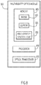
- FIG. 8 is a block diagram of a multi-identity optics module 800 that is configured to implement the techniques presented herein.
- the multi-identity optics module 800 includes a memory 805, one or more processors 810, and optical transceiver 815.
- the memory 805 includes NVRAM 820, EEPROM 825, and multi-identity control logic 830.
- the one or more processors 810 are configured to execute instructions stored in the memory 805 (e.g., multi-identity control logic 830). When executed by the one or more processors 810, the multi-identity control logic 830 enables the multi-identity optics module 800 to perform the multi-identity operations described herein in connection with FIGs. 1-7C .
- the memory 805 may be read only memory (ROM), random access memory (RAM), magnetic disk storage media devices, optical storage media devices, flash memory devices, electrical, optical, or other physical/tangible memory storage devices.
- the memory 805 may comprise one or more tangible (non-transitory) computer readable storage media (e.g., a memory device) encoded with software comprising computer executable instructions and when the software is executed (by the processor 810) it is operable to perform the operations described herein.
- FIG. 9 is a generalized flowchart 900 of a method in accordance with examples presented herein.
- an optics module sends, to a host module, a pin signal indicating that an optics module is plugged into the host module, wherein the optics module is configured to operate at at least a first data rate and a second data rate.
- the optics module receives, from the host module, an indication of a host data rate.
- the optics module determines whether there is clock and data recovery loss of lock between the first data rate and the host data rate.
- the optics module initializes at the second data rate if the second data rate matches the host data rate.
- the multi-identity multi-rate optics modules described herein are generally compatible with single-rate platforms (e.g., legacy platforms). As such, these optics modules may directly replace single-rate optics without requiring a change to the platform software driver.
- the EEPROM maps stored in the multi-identity multi-rate optics modules may comply with the appropriate multi-source agreement (MSA) in accordance with the proper MSA compliance codes.
- MSA multi-source agreement
Landscapes
- Physics & Mathematics (AREA)
- Engineering & Computer Science (AREA)
- Electromagnetism (AREA)
- Computer Networks & Wireless Communication (AREA)
- Signal Processing (AREA)
- General Physics & Mathematics (AREA)
- Theoretical Computer Science (AREA)
- Optics & Photonics (AREA)
- General Engineering & Computer Science (AREA)
- Optical Communication System (AREA)
Claims (14)
- Verfahren, das aufweist:Senden, an ein Host-Modul, eines Pin-Signals, das angibt, dass ein Optikmodul in das Host-Modul eingesteckt ist, wobei das Optikmodul dazu konfiguriert ist, mit wenigstens einer ersten Datenrate und einer zweiten Datenrate zu arbeiten (910);Empfangen, von dem Host-Modul, einer Angabe einer Host-Datenrate (920);Speichern eines ersten elektrisch löschbaren programmierbaren Festspeicherabbilds in einem hostzugreifbaren Speicherpuffer, wobei das erste elektrisch löschbare programmierbare Festspeicherabbild die erste Datenrate spezifiziert;Ermitteln, ob zwischen der ersten Datenrate und der Host-Datenrate Takt- und Datenwiederherstellungs-Sperrverlust vorliegt (930);wenn ermittelt, wird, dass zwischen der ersten Datenrate und der Host-Datenrate Takt- und Datenwiederherstellungs-Sperrverlust vorliegt, Initialisieren des Optikmoduls mit der zweiten Datenrate.
- Verfahren nach Anspruch 1, das des Weiteren aufweist:Ermitteln, ob die erste Datenrate in einem nicht flüchtigen Speicher gespeichert worden ist; undwenn ermittelt wird, dass die erste Datenrate in dem nicht flüchtigen Speicher gespeichert ist, Einstellen des Optikmoduls, um mit der ersten Datenrate zu arbeiten.
- Verfahren nach einem der vorhergehenden Ansprüche, wobei das Initialisieren des Optikmoduls mit der zweiten Datenrate aufweist:Ermitteln, ob zwischen der zweiten Datenrate und der Host-Datenrate Takt- und Datenwiederherstellungs-Sperrverlust vorliegt; undwenn ermittelt wird, dass zwischen der zweiten Datenrate und der Host-Datenrate kein Takt- und Datenwiederherstellungs-Sperrverlust vorliegt, Initialisieren des Optikmoduls mit der zweiten Datenrate.
- Verfahren nach Anspruch 3, wobei das Optikmodul dazu konfiguriert ist, mit einer dritten Datenrate zu arbeiten, wobei das Verfahren des Weiteren aufweist:
wenn ermittelt wird, dass zwischen der zweiten Datenrate und der Host-Datenrate Takt- und Datenwiederherstellungs-Sperrverlust vorliegt, Initialisieren des Optikmoduls mit der dritten Datenrate. - Verfahren nach einem der vorhergehenden Ansprüche, wobei das Initialisieren des Optikmoduls mit der zweiten Datenrate, wenn die zweite Datenrate mit der Host-Datenrate übereinstimmt, aufweist:
Einstellen der Takt- und Datenwiederherstellung auf einen Umleitungsmodus. - Verfahren nach einem der vorhergehenden Ansprüche, das des Weiteren aufweist:
wenn zwischen der ersten Datenrate und der Host-Datenrate Takt- und Datenwiederherstellungs-Sperrverlust vorliegt:Senden, an das Host-Modul, eines Pin-Signals, das angibt, dass das Optikmodul nicht in das Host-Modul eingesteckt ist; undSenden, an das Host-Modul, eines weiteren Pin-Signals, das angibt, dass das Optikmodul in das Host-Modul eingesteckt ist. - Vorrichtung (800), die aufweist:einen oder mehrere optische Transceiver (815);einen oder mehrere Prozessoren (810), die mit einem Speicher (805) verbunden sind, wobei der eine oder die mehreren Prozessoren konfiguriert ist/sind zum:Senden, an ein Host-Modul, eines Pin-Signals, das angibt, dass eine Vorrichtung in das Host-Modul eingesteckt ist, wobei die Vorrichtung dazu konfiguriert ist, mit wenigstens einer ersten Datenrate und einer zweiten Datenrate zu arbeiten;Empfangen, von dem Host-Modul, einer Angabe einer Host-Datenrate;Speichern eines ersten elektrisch löschbaren programmierbaren Festspeicherabbilds in einem hostzugreifbaren Speicherpuffer, wobei das erste elektrisch löschbare programmierbare Festspeicherabbild die erste Datenrate spezifiziert;Ermitteln, ob zwischen der ersten Datenrate und der Host-Datenrate Takt- und Datenwiederherstellungs-Sperrverlust vorliegt;wenn ermittelt, wird, dass zwischen der ersten Datenrate und der Host-Datenrate Takt- und Datenwiederherstellungs-Sperrverlust vorliegt, Initialisieren der Vorrichtung mit der zweiten Datenrate.
- Vorrichtung nach Anspruch 7, wobei der eine oder die mehreren Prozessoren des Weiteren konfiguriert ist/sind zum:Ermitteln, ob die erste Datenrate in einem nicht flüchtigen Speicher gespeichert worden ist; undwenn ermittelt wird, dass die erste Datenrate in dem nicht flüchtigen Speicher gespeichert ist, Einstellen der Vorrichtung, um mit der ersten Datenrate zu arbeiten.
- Vorrichtung nach Anspruch 7 oder 8, wobei der eine oder die mehreren Prozessoren dazu konfiguriert ist/sind, die Vorrichtung mit der zweiten Datenrate zu initialisieren, wenn die zweite Datenrate mit der Host-Datenrate übereinstimmt, durch:Ermitteln, ob zwischen der zweiten Datenrate und der Host-Datenrate Takt- und Datenwiederherstellungs-Sperrverlust vorliegt; undwenn ermittelt wird, dass zwischen der zweiten Datenrate und der Host-Datenrate kein Takt- und Datenwiederherstellungs-Sperrverlust vorliegt, Initialisieren der Vorrichtung mit der zweiten Datenrate.
- Vorrichtung nach Anspruch 9, wobei die Vorrichtung dazu konfiguriert ist, mit einer dritten Datenrate zu arbeiten, wobei der eine oder die mehreren Prozessoren des Weiteren konfiguriert ist/sind zum:
wenn ermittelt wird, dass zwischen der zweiten Datenrate und der Host-Datenrate Takt- und Datenwiederherstellungs-Sperrverlust vorliegt, Initialisieren der Vorrichtung mit der dritten Datenrate. - Vorrichtung nach einem der Ansprüche 7 bis 10, wobei der eine oder die mehreren Prozessoren dazu konfiguriert ist/sind, die Vorrichtung mit der zweiten Datenrate zu initialisieren, wenn die zweite Datenrate mit der Host-Datenrate übereinstimmt, durch:
Einstellen der Takt- und Datenwiederherstellung auf einen Umleitungsmodus. - Vorrichtung nach einem der Ansprüche 7 bis 11, wobei der eine oder die mehreren Prozessoren des Weiteren konfiguriert ist/sind zum: wenn zwischen der ersten Datenrate und der Host-Datenrate Takt- und Datenwiederherstellungs-Sperrverlust vorliegt:Senden, an das Host-Modul, eines Pin-Signals, das angibt, dass die Vorrichtung nicht in das Host-Modul eingesteckt ist; undSenden, an das Host-Modul, eines weiteren Pin-Signals, das angibt, dass die Vorrichtung in das Host-Modul eingesteckt ist.
- System, das die Vorrichtung nach einem der Ansprüche 7 bis 12 und ein Host-Modul aufweist.
- Computerlesbares Medium, das Befehle zum Ausführen des Verfahrens nach einem der Ansprüche 1 bis 7 aufweist.
Applications Claiming Priority (3)
| Application Number | Priority Date | Filing Date | Title |
|---|---|---|---|
| US201762462646P | 2017-02-23 | 2017-02-23 | |
| US15/499,196 US10164706B2 (en) | 2017-02-23 | 2017-04-27 | Multi-identity optics modules |
| PCT/US2018/018879 WO2018156533A1 (en) | 2017-02-23 | 2018-02-21 | Multi-identity optics modules |
Publications (2)
| Publication Number | Publication Date |
|---|---|
| EP3586239A1 EP3586239A1 (de) | 2020-01-01 |
| EP3586239B1 true EP3586239B1 (de) | 2021-01-27 |
Family
ID=63166654
Family Applications (1)
| Application Number | Title | Priority Date | Filing Date |
|---|---|---|---|
| EP18708550.1A Active EP3586239B1 (de) | 2017-02-23 | 2018-02-21 | Multiidentitäts-optikmodule |
Country Status (4)
| Country | Link |
|---|---|
| US (2) | US10164706B2 (de) |
| EP (1) | EP3586239B1 (de) |
| CN (1) | CN110325973B (de) |
| WO (1) | WO2018156533A1 (de) |
Families Citing this family (7)
| Publication number | Priority date | Publication date | Assignee | Title |
|---|---|---|---|---|
| US10164706B2 (en) | 2017-02-23 | 2018-12-25 | Cisco Technology, Inc. | Multi-identity optics modules |
| CN111049576B (zh) * | 2019-12-27 | 2022-03-11 | 深圳市光为光通信科技有限公司 | 一种光模块los告警的方法 |
| TWI749732B (zh) * | 2020-08-26 | 2021-12-11 | 佳必琪國際股份有限公司 | 光模組及其訊號處理方法 |
| JP7585664B2 (ja) * | 2020-08-27 | 2024-11-19 | 住友電気工業株式会社 | 光トランシーバおよびその制御方法 |
| US11777609B2 (en) | 2022-01-27 | 2023-10-03 | Cisco Technology, Inc. | Optical transceiver misconnection discovery |
| TWI802287B (zh) * | 2022-02-22 | 2023-05-11 | 佳必琪國際股份有限公司 | 小封裝可插拔收發器 |
| CN117424643A (zh) * | 2023-12-18 | 2024-01-19 | 科谱半导体(天津)有限公司 | 光通信方法、系统、存储介质及设备 |
Family Cites Families (13)
| Publication number | Priority date | Publication date | Assignee | Title |
|---|---|---|---|---|
| US6862322B1 (en) | 2000-05-19 | 2005-03-01 | International Business Machines Corporation | Switchable-bandwidth optical receiver |
| US7486894B2 (en) | 2002-06-25 | 2009-02-03 | Finisar Corporation | Transceiver module and integrated circuit with dual eye openers |
| US7664401B2 (en) | 2002-06-25 | 2010-02-16 | Finisar Corporation | Apparatus, system and methods for modifying operating characteristics of optoelectronic devices |
| US7561855B2 (en) * | 2002-06-25 | 2009-07-14 | Finisar Corporation | Transceiver module and integrated circuit with clock and data recovery clock diplexing |
| CN101098205A (zh) * | 2006-06-27 | 2008-01-02 | 中兴通讯股份有限公司 | 一种实现任意速率业务接入信号的恢复装置及控制方法 |
| EP2449698A4 (de) | 2009-06-30 | 2015-01-28 | Ericsson Telefon Ab L M | Verfahren und vorrichtung zur aktivierung von verknüpfungsstatusmeldungen |
| CN101800603B (zh) * | 2010-02-11 | 2012-12-12 | 瑞斯康达科技发展股份有限公司 | 光网络中根据速率进行自适应的方法和一种信号传输装置 |
| US8255582B2 (en) * | 2010-07-09 | 2012-08-28 | Sae Magnetics (H.K.) Ltd. | Optical communication module, universal serial bus cable with the same and processing method of data transfer thereof |
| US8660424B2 (en) * | 2010-08-26 | 2014-02-25 | Cisco Technology, Inc. | Scalable high speed gigabit active bundle link and tester |
| CN102547491B (zh) * | 2010-12-29 | 2015-12-16 | 中兴通讯股份有限公司 | 光线路终端、光网络单元和无源光网络系统 |
| US8816776B2 (en) | 2012-11-13 | 2014-08-26 | Lsi Corporation | Loss of lock detector for clock and data recovery system |
| US9438346B2 (en) | 2014-01-13 | 2016-09-06 | Cisco Technology, Inc. | Dual rate transceiver |
| US10164706B2 (en) | 2017-02-23 | 2018-12-25 | Cisco Technology, Inc. | Multi-identity optics modules |
-
2017
- 2017-04-27 US US15/499,196 patent/US10164706B2/en active Active
-
2018
- 2018-02-21 WO PCT/US2018/018879 patent/WO2018156533A1/en not_active Ceased
- 2018-02-21 CN CN201880013404.0A patent/CN110325973B/zh active Active
- 2018-02-21 EP EP18708550.1A patent/EP3586239B1/de active Active
- 2018-11-09 US US16/185,232 patent/US10419108B2/en active Active
Non-Patent Citations (1)
| Title |
|---|
| None * |
Also Published As
| Publication number | Publication date |
|---|---|
| US10419108B2 (en) | 2019-09-17 |
| US20190081699A1 (en) | 2019-03-14 |
| CN110325973B (zh) | 2023-07-18 |
| US10164706B2 (en) | 2018-12-25 |
| CN110325973A (zh) | 2019-10-11 |
| WO2018156533A1 (en) | 2018-08-30 |
| EP3586239A1 (de) | 2020-01-01 |
| US20180241467A1 (en) | 2018-08-23 |
Similar Documents
| Publication | Publication Date | Title |
|---|---|---|
| EP3586239B1 (de) | Multiidentitäts-optikmodule | |
| KR102721882B1 (ko) | 초기화 방법 및 관련 제어기, 메모리 장치 및 호스트 | |
| US7069369B2 (en) | Extended-Secure-Digital interface using a second protocol for faster transfers | |
| TWI709859B (zh) | 安全數位卡之方法、快閃記憶體控制器以及電子裝置 | |
| US20100224684A1 (en) | Smart card reader | |
| CN103299317B (zh) | 用于管理主元件与一组至少两个辅助元件之间的信息交换的方法和设备 | |
| US10466756B2 (en) | Host apparatus and expansion device adaptable to low voltage signaling | |
| US20060047982A1 (en) | Mult-interface auto-switch circuit and memory device with dual interface auto-switch circuit | |
| KR100495657B1 (ko) | 복수의 통신 모드들을 갖는 집적 회로 장치 및 그것의동작 방법 | |
| CN102004708A (zh) | 管理装置及其操作方法 | |
| EP1496436B1 (de) | Verfahren und Vorrichtung zur Rücksetzung von Chipkartenvorrichtung in Stummsmodus | |
| CN103268143B (zh) | 一种usb移动设备实现无电存储的方法 | |
| US9824046B2 (en) | Using USB signaling to trigger a device to enter a mode of operation | |
| CN108021402B (zh) | 开机控制方法及处理设备 | |
| US20140365806A1 (en) | Peripheral apparatus and control method thereof | |
| CN116366486A (zh) | 用于高速信令互连的可靠链路管理 | |
| CN209746647U (zh) | 一种使用在智能锁上的数据防护单元 | |
| CN108513656A (zh) | 控制方法、usb系统和电子装置 | |
| US20140237285A1 (en) | Single-pin command technique for mode selection and internal data access | |
| US5586272A (en) | Asynchronous data transfers among a plurality of computer devices | |
| KR20080042271A (ko) | Usb 연결을 감지하는 usb 장치 |
Legal Events
| Date | Code | Title | Description |
|---|---|---|---|
| STAA | Information on the status of an ep patent application or granted ep patent |
Free format text: STATUS: UNKNOWN |
|
| STAA | Information on the status of an ep patent application or granted ep patent |
Free format text: STATUS: THE INTERNATIONAL PUBLICATION HAS BEEN MADE |
|
| PUAI | Public reference made under article 153(3) epc to a published international application that has entered the european phase |
Free format text: ORIGINAL CODE: 0009012 |
|
| STAA | Information on the status of an ep patent application or granted ep patent |
Free format text: STATUS: REQUEST FOR EXAMINATION WAS MADE |
|
| 17P | Request for examination filed |
Effective date: 20190916 |
|
| AK | Designated contracting states |
Kind code of ref document: A1 Designated state(s): AL AT BE BG CH CY CZ DE DK EE ES FI FR GB GR HR HU IE IS IT LI LT LU LV MC MK MT NL NO PL PT RO RS SE SI SK SM TR |
|
| AX | Request for extension of the european patent |
Extension state: BA ME |
|
| DAV | Request for validation of the european patent (deleted) | ||
| DAX | Request for extension of the european patent (deleted) | ||
| GRAP | Despatch of communication of intention to grant a patent |
Free format text: ORIGINAL CODE: EPIDOSNIGR1 |
|
| STAA | Information on the status of an ep patent application or granted ep patent |
Free format text: STATUS: GRANT OF PATENT IS INTENDED |
|
| INTG | Intention to grant announced |
Effective date: 20200904 |
|
| GRAS | Grant fee paid |
Free format text: ORIGINAL CODE: EPIDOSNIGR3 |
|
| GRAA | (expected) grant |
Free format text: ORIGINAL CODE: 0009210 |
|
| STAA | Information on the status of an ep patent application or granted ep patent |
Free format text: STATUS: THE PATENT HAS BEEN GRANTED |
|
| AK | Designated contracting states |
Kind code of ref document: B1 Designated state(s): AL AT BE BG CH CY CZ DE DK EE ES FI FR GB GR HR HU IE IS IT LI LT LU LV MC MK MT NL NO PL PT RO RS SE SI SK SM TR |
|
| REG | Reference to a national code |
Ref country code: GB Ref legal event code: FG4D |
|
| REG | Reference to a national code |
Ref country code: CH Ref legal event code: EP |
|
| REG | Reference to a national code |
Ref country code: AT Ref legal event code: REF Ref document number: 1358985 Country of ref document: AT Kind code of ref document: T Effective date: 20210215 |
|
| REG | Reference to a national code |
Ref country code: IE Ref legal event code: FG4D |
|
| REG | Reference to a national code |
Ref country code: DE Ref legal event code: R096 Ref document number: 602018012315 Country of ref document: DE |
|
| REG | Reference to a national code |
Ref country code: NL Ref legal event code: MP Effective date: 20210127 |
|
| REG | Reference to a national code |
Ref country code: LT Ref legal event code: MG9D |
|
| REG | Reference to a national code |
Ref country code: AT Ref legal event code: MK05 Ref document number: 1358985 Country of ref document: AT Kind code of ref document: T Effective date: 20210127 |
|
| PG25 | Lapsed in a contracting state [announced via postgrant information from national office to epo] |
Ref country code: NO Free format text: LAPSE BECAUSE OF FAILURE TO SUBMIT A TRANSLATION OF THE DESCRIPTION OR TO PAY THE FEE WITHIN THE PRESCRIBED TIME-LIMIT Effective date: 20210427 Ref country code: PT Free format text: LAPSE BECAUSE OF FAILURE TO SUBMIT A TRANSLATION OF THE DESCRIPTION OR TO PAY THE FEE WITHIN THE PRESCRIBED TIME-LIMIT Effective date: 20210527 Ref country code: LT Free format text: LAPSE BECAUSE OF FAILURE TO SUBMIT A TRANSLATION OF THE DESCRIPTION OR TO PAY THE FEE WITHIN THE PRESCRIBED TIME-LIMIT Effective date: 20210127 Ref country code: FI Free format text: LAPSE BECAUSE OF FAILURE TO SUBMIT A TRANSLATION OF THE DESCRIPTION OR TO PAY THE FEE WITHIN THE PRESCRIBED TIME-LIMIT Effective date: 20210127 Ref country code: HR Free format text: LAPSE BECAUSE OF FAILURE TO SUBMIT A TRANSLATION OF THE DESCRIPTION OR TO PAY THE FEE WITHIN THE PRESCRIBED TIME-LIMIT Effective date: 20210127 Ref country code: GR Free format text: LAPSE BECAUSE OF FAILURE TO SUBMIT A TRANSLATION OF THE DESCRIPTION OR TO PAY THE FEE WITHIN THE PRESCRIBED TIME-LIMIT Effective date: 20210428 Ref country code: BG Free format text: LAPSE BECAUSE OF FAILURE TO SUBMIT A TRANSLATION OF THE DESCRIPTION OR TO PAY THE FEE WITHIN THE PRESCRIBED TIME-LIMIT Effective date: 20210427 |
|
| PG25 | Lapsed in a contracting state [announced via postgrant information from national office to epo] |
Ref country code: RS Free format text: LAPSE BECAUSE OF FAILURE TO SUBMIT A TRANSLATION OF THE DESCRIPTION OR TO PAY THE FEE WITHIN THE PRESCRIBED TIME-LIMIT Effective date: 20210127 Ref country code: LV Free format text: LAPSE BECAUSE OF FAILURE TO SUBMIT A TRANSLATION OF THE DESCRIPTION OR TO PAY THE FEE WITHIN THE PRESCRIBED TIME-LIMIT Effective date: 20210127 Ref country code: PL Free format text: LAPSE BECAUSE OF FAILURE TO SUBMIT A TRANSLATION OF THE DESCRIPTION OR TO PAY THE FEE WITHIN THE PRESCRIBED TIME-LIMIT Effective date: 20210127 Ref country code: AT Free format text: LAPSE BECAUSE OF FAILURE TO SUBMIT A TRANSLATION OF THE DESCRIPTION OR TO PAY THE FEE WITHIN THE PRESCRIBED TIME-LIMIT Effective date: 20210127 Ref country code: SE Free format text: LAPSE BECAUSE OF FAILURE TO SUBMIT A TRANSLATION OF THE DESCRIPTION OR TO PAY THE FEE WITHIN THE PRESCRIBED TIME-LIMIT Effective date: 20210127 |
|
| PG25 | Lapsed in a contracting state [announced via postgrant information from national office to epo] |
Ref country code: IS Free format text: LAPSE BECAUSE OF FAILURE TO SUBMIT A TRANSLATION OF THE DESCRIPTION OR TO PAY THE FEE WITHIN THE PRESCRIBED TIME-LIMIT Effective date: 20210527 |
|
| REG | Reference to a national code |
Ref country code: BE Ref legal event code: MM Effective date: 20210228 |
|
| REG | Reference to a national code |
Ref country code: DE Ref legal event code: R097 Ref document number: 602018012315 Country of ref document: DE |
|
| PG25 | Lapsed in a contracting state [announced via postgrant information from national office to epo] |
Ref country code: SM Free format text: LAPSE BECAUSE OF FAILURE TO SUBMIT A TRANSLATION OF THE DESCRIPTION OR TO PAY THE FEE WITHIN THE PRESCRIBED TIME-LIMIT Effective date: 20210127 Ref country code: LI Free format text: LAPSE BECAUSE OF NON-PAYMENT OF DUE FEES Effective date: 20210228 Ref country code: MC Free format text: LAPSE BECAUSE OF FAILURE TO SUBMIT A TRANSLATION OF THE DESCRIPTION OR TO PAY THE FEE WITHIN THE PRESCRIBED TIME-LIMIT Effective date: 20210127 Ref country code: EE Free format text: LAPSE BECAUSE OF FAILURE TO SUBMIT A TRANSLATION OF THE DESCRIPTION OR TO PAY THE FEE WITHIN THE PRESCRIBED TIME-LIMIT Effective date: 20210127 Ref country code: CZ Free format text: LAPSE BECAUSE OF FAILURE TO SUBMIT A TRANSLATION OF THE DESCRIPTION OR TO PAY THE FEE WITHIN THE PRESCRIBED TIME-LIMIT Effective date: 20210127 Ref country code: CH Free format text: LAPSE BECAUSE OF NON-PAYMENT OF DUE FEES Effective date: 20210228 Ref country code: LU Free format text: LAPSE BECAUSE OF NON-PAYMENT OF DUE FEES Effective date: 20210221 |
|
| PG25 | Lapsed in a contracting state [announced via postgrant information from national office to epo] |
Ref country code: DK Free format text: LAPSE BECAUSE OF FAILURE TO SUBMIT A TRANSLATION OF THE DESCRIPTION OR TO PAY THE FEE WITHIN THE PRESCRIBED TIME-LIMIT Effective date: 20210127 Ref country code: SK Free format text: LAPSE BECAUSE OF FAILURE TO SUBMIT A TRANSLATION OF THE DESCRIPTION OR TO PAY THE FEE WITHIN THE PRESCRIBED TIME-LIMIT Effective date: 20210127 Ref country code: RO Free format text: LAPSE BECAUSE OF FAILURE TO SUBMIT A TRANSLATION OF THE DESCRIPTION OR TO PAY THE FEE WITHIN THE PRESCRIBED TIME-LIMIT Effective date: 20210127 |
|
| PLBE | No opposition filed within time limit |
Free format text: ORIGINAL CODE: 0009261 |
|
| STAA | Information on the status of an ep patent application or granted ep patent |
Free format text: STATUS: NO OPPOSITION FILED WITHIN TIME LIMIT |
|
| 26N | No opposition filed |
Effective date: 20211028 |
|
| PG25 | Lapsed in a contracting state [announced via postgrant information from national office to epo] |
Ref country code: ES Free format text: LAPSE BECAUSE OF FAILURE TO SUBMIT A TRANSLATION OF THE DESCRIPTION OR TO PAY THE FEE WITHIN THE PRESCRIBED TIME-LIMIT Effective date: 20210127 Ref country code: IE Free format text: LAPSE BECAUSE OF NON-PAYMENT OF DUE FEES Effective date: 20210221 Ref country code: AL Free format text: LAPSE BECAUSE OF FAILURE TO SUBMIT A TRANSLATION OF THE DESCRIPTION OR TO PAY THE FEE WITHIN THE PRESCRIBED TIME-LIMIT Effective date: 20210127 |
|
| PG25 | Lapsed in a contracting state [announced via postgrant information from national office to epo] |
Ref country code: SI Free format text: LAPSE BECAUSE OF FAILURE TO SUBMIT A TRANSLATION OF THE DESCRIPTION OR TO PAY THE FEE WITHIN THE PRESCRIBED TIME-LIMIT Effective date: 20210127 |
|
| PG25 | Lapsed in a contracting state [announced via postgrant information from national office to epo] |
Ref country code: IT Free format text: LAPSE BECAUSE OF FAILURE TO SUBMIT A TRANSLATION OF THE DESCRIPTION OR TO PAY THE FEE WITHIN THE PRESCRIBED TIME-LIMIT Effective date: 20210127 |
|
| PG25 | Lapsed in a contracting state [announced via postgrant information from national office to epo] |
Ref country code: IS Free format text: LAPSE BECAUSE OF FAILURE TO SUBMIT A TRANSLATION OF THE DESCRIPTION OR TO PAY THE FEE WITHIN THE PRESCRIBED TIME-LIMIT Effective date: 20210527 |
|
| PG25 | Lapsed in a contracting state [announced via postgrant information from national office to epo] |
Ref country code: BE Free format text: LAPSE BECAUSE OF NON-PAYMENT OF DUE FEES Effective date: 20210228 |
|
| PG25 | Lapsed in a contracting state [announced via postgrant information from national office to epo] |
Ref country code: NL Free format text: LAPSE BECAUSE OF NON-PAYMENT OF DUE FEES Effective date: 20210127 Ref country code: CY Free format text: LAPSE BECAUSE OF FAILURE TO SUBMIT A TRANSLATION OF THE DESCRIPTION OR TO PAY THE FEE WITHIN THE PRESCRIBED TIME-LIMIT Effective date: 20210127 |
|
| P01 | Opt-out of the competence of the unified patent court (upc) registered |
Effective date: 20230525 |
|
| PG25 | Lapsed in a contracting state [announced via postgrant information from national office to epo] |
Ref country code: HU Free format text: LAPSE BECAUSE OF FAILURE TO SUBMIT A TRANSLATION OF THE DESCRIPTION OR TO PAY THE FEE WITHIN THE PRESCRIBED TIME-LIMIT; INVALID AB INITIO Effective date: 20180221 |
|
| PG25 | Lapsed in a contracting state [announced via postgrant information from national office to epo] |
Ref country code: MK Free format text: LAPSE BECAUSE OF FAILURE TO SUBMIT A TRANSLATION OF THE DESCRIPTION OR TO PAY THE FEE WITHIN THE PRESCRIBED TIME-LIMIT Effective date: 20210127 |
|
| PG25 | Lapsed in a contracting state [announced via postgrant information from national office to epo] |
Ref country code: TR Free format text: LAPSE BECAUSE OF FAILURE TO SUBMIT A TRANSLATION OF THE DESCRIPTION OR TO PAY THE FEE WITHIN THE PRESCRIBED TIME-LIMIT Effective date: 20210127 |
|
| PG25 | Lapsed in a contracting state [announced via postgrant information from national office to epo] |
Ref country code: MT Free format text: LAPSE BECAUSE OF FAILURE TO SUBMIT A TRANSLATION OF THE DESCRIPTION OR TO PAY THE FEE WITHIN THE PRESCRIBED TIME-LIMIT Effective date: 20210127 |
|
| PGFP | Annual fee paid to national office [announced via postgrant information from national office to epo] |
Ref country code: GB Payment date: 20260206 Year of fee payment: 9 |
|
| PGFP | Annual fee paid to national office [announced via postgrant information from national office to epo] |
Ref country code: DE Payment date: 20260113 Year of fee payment: 9 |
|
| PGFP | Annual fee paid to national office [announced via postgrant information from national office to epo] |
Ref country code: FR Payment date: 20260206 Year of fee payment: 9 |