EP3579421A1 - Analog-to-digital conversion with sampling capacitor pre-charging - Google Patents
Analog-to-digital conversion with sampling capacitor pre-charging Download PDFInfo
- Publication number
- EP3579421A1 EP3579421A1 EP19177518.8A EP19177518A EP3579421A1 EP 3579421 A1 EP3579421 A1 EP 3579421A1 EP 19177518 A EP19177518 A EP 19177518A EP 3579421 A1 EP3579421 A1 EP 3579421A1
- Authority
- EP
- European Patent Office
- Prior art keywords
- input signal
- sampling
- sampling capacitor
- adc
- charge
- Prior art date
- Legal status (The legal status is an assumption and is not a legal conclusion. Google has not performed a legal analysis and makes no representation as to the accuracy of the status listed.)
- Withdrawn
Links
Images


Classifications
-
- G—PHYSICS
- G11—INFORMATION STORAGE
- G11C—STATIC STORES
- G11C27/00—Electric analogue stores, e.g. for storing instantaneous values
- G11C27/02—Sample-and-hold arrangements
-
- H—ELECTRICITY
- H03—ELECTRONIC CIRCUITRY
- H03M—CODING; DECODING; CODE CONVERSION IN GENERAL
- H03M1/00—Analogue/digital conversion; Digital/analogue conversion
- H03M1/12—Analogue/digital converters
- H03M1/124—Sampling or signal conditioning arrangements specially adapted for A/D converters
- H03M1/1245—Details of sampling arrangements or methods
-
- H—ELECTRICITY
- H03—ELECTRONIC CIRCUITRY
- H03M—CODING; DECODING; CODE CONVERSION IN GENERAL
- H03M1/00—Analogue/digital conversion; Digital/analogue conversion
-
- H—ELECTRICITY
- H03—ELECTRONIC CIRCUITRY
- H03M—CODING; DECODING; CODE CONVERSION IN GENERAL
- H03M1/00—Analogue/digital conversion; Digital/analogue conversion
- H03M1/10—Calibration or testing
-
- H—ELECTRICITY
- H03—ELECTRONIC CIRCUITRY
- H03M—CODING; DECODING; CODE CONVERSION IN GENERAL
- H03M1/00—Analogue/digital conversion; Digital/analogue conversion
- H03M1/12—Analogue/digital converters
-
- H—ELECTRICITY
- H03—ELECTRONIC CIRCUITRY
- H03M—CODING; DECODING; CODE CONVERSION IN GENERAL
- H03M1/00—Analogue/digital conversion; Digital/analogue conversion
- H03M1/66—Digital/analogue converters
- H03M1/74—Simultaneous conversion
- H03M1/80—Simultaneous conversion using weighted impedances
- H03M1/802—Simultaneous conversion using weighted impedances using capacitors, e.g. neuron-mos transistors, charge coupled devices
Definitions
- Embodiments relate generally to analog-to-digital conversion, and more particularly, embodiments of the subject matter relate to analog-to-digital converters (ADCs) and the conversion of weakly driven analog signals.
- ADCs analog-to-digital converters
- ADC's are electronic devices that can be implemented to provide such conversions.
- weakly driven signals are those with relatively large source impedance (e.g., a source impedance of greater than 1 Mega ohm).
- a signal having such a relatively large source impedance can have a temporarily drop in voltage with even a moderate current flow. This temporary drop of the voltage can cause a variety of unwanted effects on its associated system.
- the weakly driven signal is a reference signal used to provide a reference voltage during operation of the device.
- the voltage of the reference signal can temporarily drop below a critical level. This temporary drop of the reference signal below the critical level can have a variety of unwanted effects. For example, in some applications the temporary drop in voltage of the reference signal may cause a system reset or other unwanted event.
- the embodiments described herein can provide for accurate analog-to-digital conversion while reducing the occurrence of unwanted events. Specifically, the embodiments described herein provide systems and methods for analog-to-digital conversion that can reduce the likelihood of excessive voltage drop during the conversion of weakly driven signals while still providing the ability to perform an accurate analog-to-digital conversion.
- the embodiments described herein reduce the likelihood of excessive voltage drop during the conversion of weakly driven signals by pre-charging the sampling capacitor used in the conversion.
- the embodiments selectively apply an input signal that can be weakly driven and a buffered input signal to the sampling capacitor.
- the embodiments can apply the buffered input signal to the sampling capacitor for a first sampling cycle to pre-charge the sampling capacitor, and then directly apply the unbuffered input signal to the sampling capacitor for a second sampling cycle to final-charge the sampling capacitor.
- a digital output corresponding to the charge of the sampling capacitor is generated.
- the pre-charging of the sampling capacitor during the first sampling cycle occurs with a buffered input signal
- this use of the buffered input signal can reduce the amount of voltage drop that occurs in the input signal during both the pre-charge and final-charge.
- the use of the buffer to generate the buffered input signal will significantly reduce the voltage drop that would otherwise occur during the pre-charge because of the increased current drive provided by the buffer.
- the input signal can be directly applied to the sampling capacitor without causing an excessive amount of voltage drop because the sampling capacitor already contains significant charge and is relatively near the final voltage before the input signal is directly applied.
- the embodiments described herein can both reduce the likelihood of excessive voltage drop during the conversion of weakly driven signals while also providing an accurate analog-to-digital conversion of those weakly driven signals.
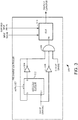
- FIG. 1 a schematic view of a portion of an analog-to-digital converter (ADC) 100 is illustrated.
- ADC 100 includes a buffer 102, a pre-charge controller 104, a sampling capacitor 106, and a converter 108.
- the ADC 100 can facilitate the digital conversion of analog input signals, including weakly driven input signals, using the pre-charge controller 104.
- the pre-charge controller 104 is configured to selectively apply an input signal to the sampling capacitor 106. Specifically, the input signal is selectively applied to the sampling capacitor 106 directly and through the buffer 102.
- the pre-charge controller 104 can be configured to apply a buffered input signal generated by the buffer 102 to the sampling capacitor 106 for a first sampling cycle to pre-charge the sampling capacitor 106.
- the pre-charge controller 104 can be configured to next directly apply the input signal to the sampling capacitor 106 for a second sampling cycle to put a final charge on the sampling capacitor 106.
- the converter 108 can generate digital output corresponding to the final charge of the sampling capacitor 106.
- the use of the two-step charging procedure can significantly reduce the amount of voltage drop that would otherwise occur during charging of the sampling capacitor 106.
- the use the of the buffer 102 to generate the buffered input signal will significantly reduce the voltage drop that would otherwise occur during the pre-charging step because of the increased current drive provided by the buffer 102.
- the potential for voltage drop is also reduced because the previously applied charge on the sampling capacitor 106 reduces the voltage difference between the input signal and the sampling capacitor 106 and thus reduces the current draw from the input signal during the final charging step.
- the final charging of the sampling capacitor 106 is performed directly from the input signal, the final charge on the sampling capacitor 106 will accurately reflect the input signal without any potential offset being introduced by the buffer 102 or other such device.
- the final voltage on the sampling capacitor 106 will accurately reflect the input signal voltage.
- the digital output generated by the converter 108 will thus accurately reflect the input signal, without any offset or other error caused by the buffer 102.
- the pre-charge controller 104 can be implemented to provide this two-stage charging of the sampling capacitor 106 with variety of circuits, structures and devices.
- pre-charge controller 104 includes a switch configured to selectively switch between the buffered input signal and the unbuffered, directly applied input signal. In some embodiments, this switch can be implemented with a suitable multiplexer.
- the pre-charge controller 104 is configured to receive an end-of-sampling signal from the converter 108. In such an embodiment the pre-charge controller 104 can be configured to switch between applying the buffered input signal to the sampling capacitor 106 and applying the input signal to the sampling capacitor 106 in response to the end-of-sampling signal.
- the pre-charge controller 104 can be implemented such that the first sampling cycle and the second sampling cycle are consecutive sampling cycles in the ADC.
- the buffer 102 can be implemented with any suitable buffer, including a variety of unity gain buffers commonly used.
- the sampling capacitor 106 can be implemented with any suitable capacitor design and technology.
- the converter 108 can likewise be implemented with any suitable type of analog-to-digital conversion techniques and devices.
- the embodiments described herein can be used to provide accurate conversion of a variety of input signals, including weakly driven input signals.
- these embodiments can be used to provide conversion of reference signals used for a variety of purposes, including band gap reference signals.
- these input signals can include both reference signals that are on the same semiconductor die with the ADC 100 and input signals that are from sources external to the die.
- the method 200 can facilitate the accurate digital conversion of analog input signals, including weakly driven input signals using a two-step charging procedure.
- the first step 202 is to apply an input signal to the input of the analog-to-digital converter (ADC).
- ADC analog-to-digital converter
- this input signal can be any suitable type of analog value, including weakly driven signals such as reference signals, including band gap reference signals.
- this input signal can originate from outside the device or within the device. In any case the input signal provides the values that are to be converted to a digital output.
- the next step 204 is to buffer the input signal to generate a buffered input signal.
- a variety of devices can be used to buffer the input signal, including any suitable unity gain buffer. So generated by a suitable buffer, the buffered input signal can be more strongly driven than the original input signal.
- the next step 206 is to apply the buffered input signal to the sampling capacitor for a first sampling cycle. This step puts a pre-charge on the sampling capacitor. Again, the use of the buffered input signal to pre-charge the sampling capacitor can significantly reduce the voltage drop that would otherwise occur during charging of the sampling capacitor because of the increased current drive in the buffered input signal.
- the next step 208 is to apply the input signal directly to the sampling capacitor for a second sampling cycle. This step puts a final charge on the sampling capacitor. The likelihood of excessive voltage drop on the input signal occurring during this step is again reduced because the previously applied pre-charge reduces the voltage difference between the input signal and the sampling capacitor, and thus reduces the current required from the input signal during the step 208. Thus, even a weakly driven signal such a band-gap reference signal will not have an excessive voltage drop during the final charging that occurs in step 208.
- step 208 charges the sampling capacitor directly from the input signal, the final charge on the sampling capacitor can more accurately reflect the input signal without any potential offset being introduced by any buffers or similar devices. This results in the final voltage on the sampling capacitor that more accurately represents the input signal voltage, even when the original input signal is a relatively small and weakly driven band-gap reference signal.
- the next step 210 is to generate a digital output corresponding to the final charge on the sampling capacitor.
- This step can be performed using any suitable analog-to-digital conversion techniques and methods.
- the digital output generated by step 210 can more accurately reflect the input signal, without any offset or other error caused by buffers or similar devices.
- the pre-charge controller 300 is an example of the type of controller that can be used in ADC 100 and method 200 described above.
- the pre-charge controller 300 includes an async set flip flop 302, inverters 304 and 306, AND gate 308, and multiplexer (MUX) 310.
- the pre-charge controller 300 receives an input signal, a buffered input signal, an async set signal, an end-of-sampling signal, and a channel enable signal. With these inputs, the pre-charge controller 300 selectively applies the input signal and the buffered input signal to the sampling capacitor.
- the async set signal is applied to the SET input of the flip flop 302.
- the end-of-sampling signal is applied to the clock input of the flip flop 302.
- the Q output of the flip flop 302 is inverted and fed back to the D input of the flip flop 302.
- the inverted output of the flip flop 302 is also applied at the AND gate 308, along with the inverted end-of-sampling signal and channel enable signal. So configured, the AND gate 308 asserts a MUX enable signal when the inverted flip-flop output, inverted end of sampling signal, and channel enable signal are all asserted.
- the MUX 310 operates to selectively output the buffered input signal or the input signal to the sampling capacitor. Specifically, when the MUX enable signal is non-asserted, the MUX 310 passes the buffered input signal to the sampling capacitor. In contrast, when the MUX enable signal asserted the MUX 310 passes the input signal directly to the sampling capacitor.
- a timing diagram 400 illustrates exemplary waveforms of the async set signal, the channel enable signal, the sampling start signal, the end-of-sampling signal, the end-of-conversion signal, and the MUX enable signal.
- the async set signal goes high at time T 1 when the ADC is initialized. This sets the async set flip flop 302, causing the Q output of the async set flip flop 302 to be set high. This setting of the async set flip flop 302 assures that the MUX enable signal (i.e., the output of the AND gate 308) is low and the MUX 310 is initially set to pass the buffered input signal to the sampling capacitor.
- the MUX enable signal i.e., the output of the AND gate 308
- the channel enable signal is goes high and at time T 3 the sampling start signal goes high.
- the channel enable signal going high indicates that the current channel is being activated and the sampling start signal going high is indication that the ADC is ready to start sampling.
- the sampling start signal going high thus indicates the start of the first sampling cycle during which the buffered input signal is applied to the sampling capacitor.
- the end-of-sampling signal goes high. This indicates the end of the first sampling cycle and the start of the second sampling cycle.
- the end-of-sampling signal is applied to the clock input of the async set flip flop 302 which causes the flip flop 302 to go low and the output of inverter 304 to go high.
- the end-of-sampling signal is also inverted using inverter 306 and applied to the AND gate 308.
- the end-of-sampling signal going high causes output of inverter 306 to go low and in turn the output of AND gate 308 to stay low.
- the end-of-sampling signal goes low. This causes the output of inverter 306 to go high and in turn the output of the AND gate 308 (the MUX enable signal) to go high. This causes the MUX 310 to now pass the input signal directly to the sampling capacitor during the second sampling cycle, where the first sampling cycle and the second sampling cycle are consecutive sampling cycles in the ADC.
- the end-of-sampling signal again goes high. This indicates the end of the second sampling cycle and that the conversion of the voltage on the sampling capacitor has started. Again, because the input signal was directly applied to the sampling capacitor during the second sampling cycle the final voltage on the sampling capacitor more accurately reflects the input signal voltage. Thus, the digital output generated by the conversion can more accurately reflect the input signal, without any offset or other error caused by the buffered input signal. And again, this use of the two-step charging procedure can significantly reduce the amount of voltage drop that would otherwise occur during charging of the sampling capacitor.
- the end-of-sampling signal going high at T 6 causes the async set flip flop 302 to output a high and output of inverter 304 to go low, which causes the output of the AND gate 308 (the MUX enable signal) to go low.
- the end-of-conversion signal goes high, indicating an end of the digital-to-analog conversion.
- the embodiments described herein can thus provide for accurate analog-to-digital conversion while reducing the likelihood of excessive voltage drop during the conversion of weakly driven signals. Again, these embodiments reduce the likelihood of excessive voltage drop during the conversion of weakly driven signals by pre-charging the sampling capacitor used in the conversion.
- the embodiments selectively apply an input signal that can be weakly driven and a buffered input signal to the sampling capacitor. For example, the embodiments can apply the buffered input signal to the sampling capacitor for a first sampling cycle to pre-charge the sampling capacitor, and then directly apply the unbuffered input signal to the sampling capacitor for a second sampling cycle to final-charge the sampling capacitor. With the sampling capacitor charged using the two stage charging, the digital output corresponding to the charge of the sampling capacitor is generated.
- the embodiments described herein can both reduce the likelihood of excessive voltage drop during the conversion of weakly driven signals while also providing an accurate analog-to-digital conversion of those weakly driven signals.
- an analog-to-digital converter comprising: an input configured to receive an input signal; a buffer coupled to the input, the buffer configured to receive the input signal and generate a buffered input signal; a pre-charge controller, the pre-charge controller configured to receive the input signal and the buffered input signal, and to selectively apply the input signal and buffered input signal to a sampling capacitor, where the pre-charge controller is configured to: apply the buffered input signal to the sampling capacitor for a first ADC sampling cycle to pre-charge the sampling capacitor; apply the input signal to the sampling capacitor for a second ADC sampling cycle to final-charge the sampling capacitor; and a converter configured to generate a digital output corresponding to the final-charge of the sampling capacitor.
- ADC analog-to-digital converter
- an analog-to-digital converter comprising: an input configured to receive an input signal; a unity-gain buffer coupled to the input, the buffer configured to receive the input signal and generate a buffered input signal; a pre-charge controller, the pre-charge controller including a multiplexer, the pre-charge controller configured to receive the input signal and the buffered input signal, and to selectively apply the input signal and buffered input signal to a sampling capacitor using the multiplexer, where the pre-charge controller is configured to: apply the buffered input signal to the sampling capacitor for a first ADC sampling cycle to pre-charge the sampling capacitor; in response to an end-of-sampling signal after the first ADC sampling cycle, directly apply the input signal to the sampling capacitor for a second ADC sampling cycle to final-charge the sampling capacitor, where the first ADC sampling cycle and the second ADC sampling cycle are consecutive sampling cycles; and a converter configured to generate a digital output corresponding to the final-charge of the sampling capacitor.
- ADC analog-to-digital converter
- a method of performing an analog-to-digital conversion comprising: applying an input signal to an input; buffering the input signal to generate a buffered input signal; applying the buffered input signal to a sampling capacitor for a first ADC sampling cycle to pre-charge the sampling capacitor; applying the input signal to the sampling capacitor for a second ADC sampling cycle to final-charge the sampling capacitor; and generating a digital output corresponding to the final-charge of the sampling capacitor.
- the embodiments described herein provide analog-to-digital converters and methods that can reduce the likelihood of excessive voltage drop during the conversion of weakly driven signals while still providing the ability to perform an accurate analog-to-digital conversion.
- the embodiments described herein reduce the likelihood of excessive voltage drop during the conversion of weakly driven signals by pre-charging the sampling capacitor used in the conversion.
- the embodiments can apply the buffered input signal apply to the sampling capacitor for a first sampling cycle to pre-charge the sampling capacitor (206), and then directly apply the unbuffered input signal to the sampling capacitor for a second sampling cycle to final-charge the sampling capacitor (208). With the sampling capacitor charged using the two stage charging, a digital output corresponding to the charge of the sampling capacitor is generated (210).
- a "node” means any internal or external reference point, connection point, junction, signal line, conductive element, or the like, at which a given signal, logic level, voltage, data pattern, current, or quantity is present. Furthermore, two or more nodes may be realized by one physical element (and two or more signals can be multiplexed, modulated, or otherwise distinguished even though received or output at a common mode).
- the foregoing description refers to elements or nodes or features being “connected” or “coupled” together.
- “connected” means that one element/node/feature is directly joined to (or directly communicates with) another element/node/feature, and not necessarily mechanically.
- Coupled means that one element is directly or indirectly joined to (or directly or indirectly communicates with) another element, and not necessarily mechanically.
Landscapes
- Engineering & Computer Science (AREA)
- Theoretical Computer Science (AREA)
- Analogue/Digital Conversion (AREA)
Abstract
The embodiments described herein provide analog-to-digital converters and methods that can reduce the likelihood of excessive voltage drop during the conversion of weakly driven signals while still providing the ability to perform an accurate analog-to-digital conversion. In general, the embodiments described herein reduce the likelihood of excessive voltage drop during the conversion of weakly driven signals by pre-charging the sampling capacitor used in the conversion. For example, the embodiments can apply the buffered input signal apply to the sampling capacitor for a first sampling cycle to pre-charge the sampling capacitor (206), and then directly apply the unbuffered input signal to the sampling capacitor for a second sampling cycle to final-charge the sampling capacitor (208). With the sampling capacitor charged using the two stage charging, a digital output corresponding to the charge of the sampling capacitor is generated (210).

Description
- Embodiments relate generally to analog-to-digital conversion, and more particularly, embodiments of the subject matter relate to analog-to-digital converters (ADCs) and the conversion of weakly driven analog signals.
- In many modern electronics applications, it is needed to convert an analog value to a digital value. For example, it some applications it can be needed to convert a continuous physical quantity (such as a voltage) to digital value that represents the amplitude of the physical quantity. Analog-to-digital converters (ADC's) are electronic devices that can be implemented to provide such conversions.
- One issue in ADCs is the need for conversion of weakly driven signals. In general, weakly driven signals are those with relatively large source impedance (e.g., a source impedance of greater than 1 Mega ohm). A signal having such a relatively large source impedance can have a temporarily drop in voltage with even a moderate current flow. This temporary drop of the voltage can cause a variety of unwanted effects on its associated system.
- For example, in one application the weakly driven signal is a reference signal used to provide a reference voltage during operation of the device. When such a weakly driven reference signal is measured by a traditional ADC, the voltage of the reference signal can temporarily drop below a critical level. This temporary drop of the reference signal below the critical level can have a variety of unwanted effects. For example, in some applications the temporary drop in voltage of the reference signal may cause a system reset or other unwanted event.
- Unfortunately, current techniques for analog-to-digital conversion can lack the ability to accurately measure weakly driven signals without causing such a temporary voltage drop and resulting unwanted events. Thus, what are needed are improved devices and techniques for the analog-to-digital conversion of weakly driven signals that can reduce the likelihood of excessive voltage drop during analog-to-digital conversion.
- A more complete understanding of the present invention may be derived by referring to the detailed description and claims when considered in connection with the Figures, wherein like reference numbers refer to similar items throughout the Figures, the Figures are not necessarily drawn to scale, and:
-
FIG. 1 shows a generalized block diagram of an analog-to-digital converter (ADC) in accordance with an embodiment; -
FIG. 2 shows a method of analog-to-digital conversion in accordance with an embodiment; -
FIG. 3 shows a schematic diagram of a pre-charge controller in accordance with an embodiment; and -
FIG. 4 shows a timing diagram in accordance with an embodiment. - The embodiments described herein can provide for accurate analog-to-digital conversion while reducing the occurrence of unwanted events. Specifically, the embodiments described herein provide systems and methods for analog-to-digital conversion that can reduce the likelihood of excessive voltage drop during the conversion of weakly driven signals while still providing the ability to perform an accurate analog-to-digital conversion.
- In general, the embodiments described herein reduce the likelihood of excessive voltage drop during the conversion of weakly driven signals by pre-charging the sampling capacitor used in the conversion. Specifically, the embodiments selectively apply an input signal that can be weakly driven and a buffered input signal to the sampling capacitor. For example, the embodiments can apply the buffered input signal to the sampling capacitor for a first sampling cycle to pre-charge the sampling capacitor, and then directly apply the unbuffered input signal to the sampling capacitor for a second sampling cycle to final-charge the sampling capacitor. With the sampling capacitor charged using the two stage charging, a digital output corresponding to the charge of the sampling capacitor is generated.
- In such embodiments, the pre-charging of the sampling capacitor during the first sampling cycle occurs with a buffered input signal, and this use of the buffered input signal can reduce the amount of voltage drop that occurs in the input signal during both the pre-charge and final-charge. Specifically, the use of the buffer to generate the buffered input signal will significantly reduce the voltage drop that would otherwise occur during the pre-charge because of the increased current drive provided by the buffer. Then, during the final charging of the sampling capacitor the input signal can be directly applied to the sampling capacitor without causing an excessive amount of voltage drop because the sampling capacitor already contains significant charge and is relatively near the final voltage before the input signal is directly applied.
- Furthermore, because the final charging of the sampling capacitor is performed directly from the input signal, the final charge on the sampling capacitor will accurately reflect the input signal without any potential offset being introduced by the buffer or other such intervening elements. Thus, the embodiments described herein can both reduce the likelihood of excessive voltage drop during the conversion of weakly driven signals while also providing an accurate analog-to-digital conversion of those weakly driven signals.
- Turning now to
FIG. 1 , a schematic view of a portion of an analog-to-digital converter (ADC) 100 is illustrated. The illustrated portion of ADC 100 includes abuffer 102, apre-charge controller 104, asampling capacitor 106, and aconverter 108. In accordance with the embodiments described herein, the ADC 100 can facilitate the digital conversion of analog input signals, including weakly driven input signals, using thepre-charge controller 104. - In this illustrated embodiment the
pre-charge controller 104 is configured to selectively apply an input signal to thesampling capacitor 106. Specifically, the input signal is selectively applied to thesampling capacitor 106 directly and through thebuffer 102. - As one specific example, the
pre-charge controller 104 can be configured to apply a buffered input signal generated by thebuffer 102 to thesampling capacitor 106 for a first sampling cycle to pre-charge thesampling capacitor 106. Thepre-charge controller 104 can be configured to next directly apply the input signal to thesampling capacitor 106 for a second sampling cycle to put a final charge on thesampling capacitor 106. With thesampling capacitor 106 charged using this two-step charging procedure, theconverter 108 can generate digital output corresponding to the final charge of thesampling capacitor 106. - The use of the two-step charging procedure can significantly reduce the amount of voltage drop that would otherwise occur during charging of the
sampling capacitor 106. Specifically, the use the of thebuffer 102 to generate the buffered input signal will significantly reduce the voltage drop that would otherwise occur during the pre-charging step because of the increased current drive provided by thebuffer 102. Then, during the final charging step the potential for voltage drop is also reduced because the previously applied charge on thesampling capacitor 106 reduces the voltage difference between the input signal and thesampling capacitor 106 and thus reduces the current draw from the input signal during the final charging step. - Furthermore, because the final charging of the
sampling capacitor 106 is performed directly from the input signal, the final charge on thesampling capacitor 106 will accurately reflect the input signal without any potential offset being introduced by thebuffer 102 or other such device. Thus, the final voltage on thesampling capacitor 106 will accurately reflect the input signal voltage. The digital output generated by theconverter 108 will thus accurately reflect the input signal, without any offset or other error caused by thebuffer 102. - The
pre-charge controller 104 can be implemented to provide this two-stage charging of thesampling capacitor 106 with variety of circuits, structures and devices. In one embodiment, pre-chargecontroller 104 includes a switch configured to selectively switch between the buffered input signal and the unbuffered, directly applied input signal. In some embodiments, this switch can be implemented with a suitable multiplexer. In one embodiment, thepre-charge controller 104 is configured to receive an end-of-sampling signal from theconverter 108. In such an embodiment thepre-charge controller 104 can be configured to switch between applying the buffered input signal to thesampling capacitor 106 and applying the input signal to thesampling capacitor 106 in response to the end-of-sampling signal. One specific implementation will be discussed in greater detail below with reference toFIG. 3 . Additionally, thepre-charge controller 104 can be implemented such that the first sampling cycle and the second sampling cycle are consecutive sampling cycles in the ADC. - In general, the
buffer 102 can be implemented with any suitable buffer, including a variety of unity gain buffers commonly used. Likewise, thesampling capacitor 106 can be implemented with any suitable capacitor design and technology. Theconverter 108 can likewise be implemented with any suitable type of analog-to-digital conversion techniques and devices. - As noted above, the embodiments described herein can be used to provide accurate conversion of a variety of input signals, including weakly driven input signals. For example, these embodiments can be used to provide conversion of reference signals used for a variety of purposes, including band gap reference signals. Furthermore, these input signals can include both reference signals that are on the same semiconductor die with the
ADC 100 and input signals that are from sources external to the die. - Turning now to
FIG. 2 , amethod 200 for performing an analog-to-digital conversion is illustrated. In accordance with the embodiments described herein, themethod 200 can facilitate the accurate digital conversion of analog input signals, including weakly driven input signals using a two-step charging procedure. - The first step 202 is to apply an input signal to the input of the analog-to-digital converter (ADC). As described above, this input signal can be any suitable type of analog value, including weakly driven signals such as reference signals, including band gap reference signals. Furthermore, this input signal can originate from outside the device or within the device. In any case the input signal provides the values that are to be converted to a digital output.
- The next step 204 is to buffer the input signal to generate a buffered input signal. Again, a variety of devices can be used to buffer the input signal, including any suitable unity gain buffer. So generated by a suitable buffer, the buffered input signal can be more strongly driven than the original input signal.
- The next step 206 is to apply the buffered input signal to the sampling capacitor for a first sampling cycle. This step puts a pre-charge on the sampling capacitor. Again, the use of the buffered input signal to pre-charge the sampling capacitor can significantly reduce the voltage drop that would otherwise occur during charging of the sampling capacitor because of the increased current drive in the buffered input signal.
- The next step 208 is to apply the input signal directly to the sampling capacitor for a second sampling cycle. This step puts a final charge on the sampling capacitor. The likelihood of excessive voltage drop on the input signal occurring during this step is again reduced because the previously applied pre-charge reduces the voltage difference between the input signal and the sampling capacitor, and thus reduces the current required from the input signal during the step 208. Thus, even a weakly driven signal such a band-gap reference signal will not have an excessive voltage drop during the final charging that occurs in step 208.
- Furthermore, because step 208 charges the sampling capacitor directly from the input signal, the final charge on the sampling capacitor can more accurately reflect the input signal without any potential offset being introduced by any buffers or similar devices. This results in the final voltage on the sampling capacitor that more accurately represents the input signal voltage, even when the original input signal is a relatively small and weakly driven band-gap reference signal.
- The next step 210 is to generate a digital output corresponding to the final charge on the sampling capacitor. This step can be performed using any suitable analog-to-digital conversion techniques and methods. Furthermore, because the final voltage on the sampling capacitor more accurately reflected the input signal voltage, the digital output generated by step 210 can more accurately reflect the input signal, without any offset or other error caused by buffers or similar devices.
- Turning now to
FIG. 3 , an exemplarypre-charge controller 300 is illustrated schematically. Thepre-charge controller 300 is an example of the type of controller that can be used inADC 100 andmethod 200 described above. Thepre-charge controller 300 includes an asyncset flip flop 302,inverters gate 308, and multiplexer (MUX) 310. Thepre-charge controller 300 receives an input signal, a buffered input signal, an async set signal, an end-of-sampling signal, and a channel enable signal. With these inputs, thepre-charge controller 300 selectively applies the input signal and the buffered input signal to the sampling capacitor. - Specifically, the async set signal is applied to the SET input of the
flip flop 302. The end-of-sampling signal is applied to the clock input of theflip flop 302. The Q output of theflip flop 302 is inverted and fed back to the D input of theflip flop 302. The inverted output of theflip flop 302 is also applied at the ANDgate 308, along with the inverted end-of-sampling signal and channel enable signal. So configured, the ANDgate 308 asserts a MUX enable signal when the inverted flip-flop output, inverted end of sampling signal, and channel enable signal are all asserted. - The
MUX 310 operates to selectively output the buffered input signal or the input signal to the sampling capacitor. Specifically, when the MUX enable signal is non-asserted, theMUX 310 passes the buffered input signal to the sampling capacitor. In contrast, when the MUX enable signal asserted theMUX 310 passes the input signal directly to the sampling capacitor. - Turning to
FIG. 4 , a timing diagram 400 illustrates exemplary waveforms of the async set signal, the channel enable signal, the sampling start signal, the end-of-sampling signal, the end-of-conversion signal, and the MUX enable signal. Referring now toFIGS 3 and4 together, the async set signal goes high at time T1 when the ADC is initialized. This sets the asyncset flip flop 302, causing the Q output of the asyncset flip flop 302 to be set high. This setting of the asyncset flip flop 302 assures that the MUX enable signal (i.e., the output of the AND gate 308) is low and theMUX 310 is initially set to pass the buffered input signal to the sampling capacitor. - At time T2, the channel enable signal is goes high and at time T3 the sampling start signal goes high. The channel enable signal going high indicates that the current channel is being activated and the sampling start signal going high is indication that the ADC is ready to start sampling. The sampling start signal going high thus indicates the start of the first sampling cycle during which the buffered input signal is applied to the sampling capacitor.
- At time T4 the end-of-sampling signal goes high. This indicates the end of the first sampling cycle and the start of the second sampling cycle. Again, the end-of-sampling signal is applied to the clock input of the async
set flip flop 302 which causes theflip flop 302 to go low and the output ofinverter 304 to go high. The end-of-sampling signal is also inverted usinginverter 306 and applied to the ANDgate 308. The end-of-sampling signal going high causes output ofinverter 306 to go low and in turn the output of ANDgate 308 to stay low. - At time T5 the end-of-sampling signal goes low. This causes the output of
inverter 306 to go high and in turn the output of the AND gate 308 (the MUX enable signal) to go high. This causes theMUX 310 to now pass the input signal directly to the sampling capacitor during the second sampling cycle, where the first sampling cycle and the second sampling cycle are consecutive sampling cycles in the ADC. - At time T6 the end-of-sampling signal again goes high. This indicates the end of the second sampling cycle and that the conversion of the voltage on the sampling capacitor has started. Again, because the input signal was directly applied to the sampling capacitor during the second sampling cycle the final voltage on the sampling capacitor more accurately reflects the input signal voltage. Thus, the digital output generated by the conversion can more accurately reflect the input signal, without any offset or other error caused by the buffered input signal. And again, this use of the two-step charging procedure can significantly reduce the amount of voltage drop that would otherwise occur during charging of the sampling capacitor.
- The end-of-sampling signal going high at T6 causes the async
set flip flop 302 to output a high and output ofinverter 304 to go low, which causes the output of the AND gate 308 (the MUX enable signal) to go low. At time T7 the end-of-conversion signal goes high, indicating an end of the digital-to-analog conversion. - The embodiments described herein can thus provide for accurate analog-to-digital conversion while reducing the likelihood of excessive voltage drop during the conversion of weakly driven signals. Again, these embodiments reduce the likelihood of excessive voltage drop during the conversion of weakly driven signals by pre-charging the sampling capacitor used in the conversion. Specifically, the embodiments selectively apply an input signal that can be weakly driven and a buffered input signal to the sampling capacitor. For example, the embodiments can apply the buffered input signal to the sampling capacitor for a first sampling cycle to pre-charge the sampling capacitor, and then directly apply the unbuffered input signal to the sampling capacitor for a second sampling cycle to final-charge the sampling capacitor. With the sampling capacitor charged using the two stage charging, the digital output corresponding to the charge of the sampling capacitor is generated.
- Furthermore, because the final charging the sampling capacitor is performed directly from the input signal, the final charge on the sampling capacitor will accurately reflect the input signal without any potential offset being introduced by the buffer or other such intervening elements. Thus, the embodiments described herein can both reduce the likelihood of excessive voltage drop during the conversion of weakly driven signals while also providing an accurate analog-to-digital conversion of those weakly driven signals.
- In one embodiment, an analog-to-digital converter (ADC) is provided, comprising: an input configured to receive an input signal; a buffer coupled to the input, the buffer configured to receive the input signal and generate a buffered input signal; a pre-charge controller, the pre-charge controller configured to receive the input signal and the buffered input signal, and to selectively apply the input signal and buffered input signal to a sampling capacitor, where the pre-charge controller is configured to: apply the buffered input signal to the sampling capacitor for a first ADC sampling cycle to pre-charge the sampling capacitor; apply the input signal to the sampling capacitor for a second ADC sampling cycle to final-charge the sampling capacitor; and a converter configured to generate a digital output corresponding to the final-charge of the sampling capacitor.
- In another embodiment, an analog-to-digital converter (ADC) is provided, comprising: an input configured to receive an input signal; a unity-gain buffer coupled to the input, the buffer configured to receive the input signal and generate a buffered input signal; a pre-charge controller, the pre-charge controller including a multiplexer, the pre-charge controller configured to receive the input signal and the buffered input signal, and to selectively apply the input signal and buffered input signal to a sampling capacitor using the multiplexer, where the pre-charge controller is configured to: apply the buffered input signal to the sampling capacitor for a first ADC sampling cycle to pre-charge the sampling capacitor; in response to an end-of-sampling signal after the first ADC sampling cycle, directly apply the input signal to the sampling capacitor for a second ADC sampling cycle to final-charge the sampling capacitor, where the first ADC sampling cycle and the second ADC sampling cycle are consecutive sampling cycles; and a converter configured to generate a digital output corresponding to the final-charge of the sampling capacitor.
- In another embodiment, a method of performing an analog-to-digital conversion is provided, the method comprising: applying an input signal to an input; buffering the input signal to generate a buffered input signal; applying the buffered input signal to a sampling capacitor for a first ADC sampling cycle to pre-charge the sampling capacitor; applying the input signal to the sampling capacitor for a second ADC sampling cycle to final-charge the sampling capacitor; and generating a digital output corresponding to the final-charge of the sampling capacitor.
- The embodiments described herein provide analog-to-digital converters and methods that can reduce the likelihood of excessive voltage drop during the conversion of weakly driven signals while still providing the ability to perform an accurate analog-to-digital conversion. In general, the embodiments described herein reduce the likelihood of excessive voltage drop during the conversion of weakly driven signals by pre-charging the sampling capacitor used in the conversion. For example, the embodiments can apply the buffered input signal apply to the sampling capacitor for a first sampling cycle to pre-charge the sampling capacitor (206), and then directly apply the unbuffered input signal to the sampling capacitor for a second sampling cycle to final-charge the sampling capacitor (208). With the sampling capacitor charged using the two stage charging, a digital output corresponding to the charge of the sampling capacitor is generated (210).
- For the sake of brevity, conventional techniques related to signal processing, sampling, analog-to-digital conversion, digital-to-analog conversion, analog circuit design, differential circuit design, and other functional aspects of the systems (and the individual operating components of the systems) may not be described in detail herein. Furthermore, the connecting lines shown in the various figures contained herein are intended to represent exemplary functional relationships and/or physical couplings between the various elements. It should be noted that many alternative or additional functional relationships or physical connections may be present in an embodiment of the subject matter. It should be understood that circuitry described herein may be implemented either in silicon or another semiconductor material or alternatively by software code representation thereof.
- As used herein, a "node" means any internal or external reference point, connection point, junction, signal line, conductive element, or the like, at which a given signal, logic level, voltage, data pattern, current, or quantity is present. Furthermore, two or more nodes may be realized by one physical element (and two or more signals can be multiplexed, modulated, or otherwise distinguished even though received or output at a common mode). The foregoing description refers to elements or nodes or features being "connected" or "coupled" together. As used herein, unless expressly stated otherwise, "connected" means that one element/node/feature is directly joined to (or directly communicates with) another element/node/feature, and not necessarily mechanically. Unless expressly stated otherwise, "coupled" means that one element is directly or indirectly joined to (or directly or indirectly communicates with) another element, and not necessarily mechanically. Thus, although the schematics shown in the figures depict exemplary arrangements of elements, additional intervening elements, devices, features, or components may be present in an embodiment of the depicted subject matter. In addition, certain terminology may also be used in the foregoing description for the purpose of reference only, and thus are not intended to be limiting.
- The terms "first," "second," "third," "fourth" and the like in the description and the claims are used for distinguishing between elements and not necessarily for describing a particular structural, sequential or chronological order. It is to be understood that the terms so used are interchangeable under appropriate circumstances. Furthermore, the terms "comprise," "include," "have" and any variations thereof, are intended to cover non-exclusive inclusions, such that a circuit, process, method, article, or apparatus that comprises a list of elements is not necessarily limited to those elements, but may include other elements not expressly listed or inherent to such circuit, process, method, article, or apparatus.
- The foregoing description of specific embodiments reveals the general nature of the inventive subject matter sufficiently that others can, by applying current knowledge, readily modify and/or adapt it for various applications without departing from the general concept. Therefore, such adaptations and modifications are within the meaning and range of equivalents of the disclosed embodiments. The inventive subject matter embraces all such alternatives, modifications, equivalents, and variations as fall within the spirit and broad scope of the appended claims.
Claims (15)
- An analog-to-digital converter (ADC), comprising:an input configured to receive an input signal;a buffer coupled to the input, the buffer configured to receive the input signal and generate a buffered input signal;a pre-charge controller, the pre-charge controller configured to receive the input signal and the buffered input signal, and to selectively apply the input signal and buffered input signal to a sampling capacitor, where the pre-charge controller is configured to:apply the buffered input signal to the sampling capacitor for a first ADC sampling cycle to pre-charge the sampling capacitor;apply the input signal to the sampling capacitor for a second ADC sampling cycle to final-charge the sampling capacitor; anda converter configured to generate a digital output corresponding to the final-charge of the sampling capacitor.
- The ADC of claim 1, wherein the pre-charge controller includes a switch, the switch configured to selectively switch between the buffered input signal and the input signal.
- The ADC of any preceding claim, wherein the pre-charge controller is configured to receive an end-of-sampling signal from the converter, and wherein the pre-charge controller is configured to switch between applying the buffered input signal to the sampling capacitor and applying the input signal to the sampling capacitor in response to the end-of-sampling signal.
- The ADC of any preceding claim, wherein the pre-charge controller is configured to receive a set signal configured to set the pre-charge controller in an initial state with the buffered input signal coupled to the sampling capacitor.
- The ADC of any preceding claim, wherein the buffer comprises a unity gain buffer.
- The ADC of any preceding claim, wherein the pre-charge controller is configured to directly apply the input signal to the sampling capacitor for the second ADC sampling cycle to final-charge the sampling capacitor.
- The ADC of any preceding claim, wherein the input signal comprises a weakly driven reference signal.
- The ADC of any preceding claim, wherein the ADC is formed on a semiconductor die, and wherein the input signal comprises an internal reference signal on the semiconductor die.
- The ADC of any preceding claim, wherein the input signal is a band gap reference signal.
- The ADC of any preceding claim, wherein the first ADC sampling cycle and the second ADC sampling cycle are consecutive sampling cycles in the ADC.
- A method of performing an analog-to-digital conversion, the method comprising:applying an input signal to an input;buffering the input signal to generate a buffered input signal;applying the buffered input signal to a sampling capacitor for a first ADC sampling cycle to pre-charge the sampling capacitor;applying the input signal to the sampling capacitor for a second ADC sampling cycle to final-charge the sampling capacitor; andgenerating a digital output corresponding to the final-charge of the sampling capacitor.
- The method of claim 11, wherein the step of applying the buffered input signal and the step of applying input signal comprises using a switch to selectively switch between the buffered input signal and the input signal.
- The method of claim 11 or 12, wherein the step of applying the input signal to the input for the second ADC sampling cycle is performed in response to an end-of-sampling signal.
- The method of any of claims 11 to 13, wherein the step of buffering the input signal comprising buffering the input signal with a unity gain buffer.
- The method of any of claims 11 to 14, wherein the step of applying the input signal to the input for the second ADC sampling cycle comprises directly applying the input signal to the sampling capacitor for the second ADC sampling cycle to final-charge the sampling capacitor.
Applications Claiming Priority (1)
| Application Number | Priority Date | Filing Date | Title |
|---|---|---|---|
| US15/997,525 US10312929B1 (en) | 2018-06-04 | 2018-06-04 | Analog-to-digital conversion with sampling capacitor pre-charging |
Publications (1)
| Publication Number | Publication Date |
|---|---|
| EP3579421A1 true EP3579421A1 (en) | 2019-12-11 |
Family
ID=66673327
Family Applications (1)
| Application Number | Title | Priority Date | Filing Date |
|---|---|---|---|
| EP19177518.8A Withdrawn EP3579421A1 (en) | 2018-06-04 | 2019-05-30 | Analog-to-digital conversion with sampling capacitor pre-charging |
Country Status (2)
| Country | Link |
|---|---|
| US (1) | US10312929B1 (en) |
| EP (1) | EP3579421A1 (en) |
Citations (3)
| Publication number | Priority date | Publication date | Assignee | Title |
|---|---|---|---|---|
| US8994564B2 (en) * | 2012-09-07 | 2015-03-31 | Analog Devices Technology | Analog to digital converter including a pre-charge circuit |
| US9548948B2 (en) * | 2012-08-24 | 2017-01-17 | Analog Devices Global | Input current cancellation scheme for fast channel switching systems |
| US9571118B1 (en) * | 2016-06-27 | 2017-02-14 | Freescale Semiconductor, Inc. | Pre-charge buffer for analog-to-digital converter |
Family Cites Families (4)
| Publication number | Priority date | Publication date | Assignee | Title |
|---|---|---|---|---|
| US7420490B2 (en) | 2006-07-31 | 2008-09-02 | Texas Instruments Incorporated | Pre-charge systems and methods for ADC input sampling |
| CN104678240B (en) | 2013-12-03 | 2019-03-29 | 恩智浦美国有限公司 | For testing the circuit of power supply in multiple power modes |
| US9742689B1 (en) | 2013-12-27 | 2017-08-22 | Inphi Corporation | Channel negotiation for a high speed link |
| US10001406B2 (en) * | 2016-06-07 | 2018-06-19 | Semiconductor Components Industries, Llc | Charge packet signal processing using pinned photodiode devices |
-
2018
- 2018-06-04 US US15/997,525 patent/US10312929B1/en active Active
-
2019
- 2019-05-30 EP EP19177518.8A patent/EP3579421A1/en not_active Withdrawn
Patent Citations (3)
| Publication number | Priority date | Publication date | Assignee | Title |
|---|---|---|---|---|
| US9548948B2 (en) * | 2012-08-24 | 2017-01-17 | Analog Devices Global | Input current cancellation scheme for fast channel switching systems |
| US8994564B2 (en) * | 2012-09-07 | 2015-03-31 | Analog Devices Technology | Analog to digital converter including a pre-charge circuit |
| US9571118B1 (en) * | 2016-06-27 | 2017-02-14 | Freescale Semiconductor, Inc. | Pre-charge buffer for analog-to-digital converter |
Non-Patent Citations (1)
| Title |
|---|
| DINE H ET AL: "A rail to rail, slew-boosted pre-charge buffer", 2006 IEEE INTERNATIONAL SYMPOSIUM ON CIRCUITS AND SYSTEMS 21-24 MAY 2006 ISLAND OF KOS, GREECE, IEEE - PISCATAWAY, NJ, USA, 21 May 2006 (2006-05-21), pages 4pp, XP032457646, ISBN: 978-0-7803-9389-9, DOI: 10.1109/ISCAS.2006.1692523 * |
Also Published As
| Publication number | Publication date |
|---|---|
| US10312929B1 (en) | 2019-06-04 |
Similar Documents
| Publication | Publication Date | Title |
|---|---|---|
| CN107819468B (en) | Bootstrap switch circuit | |
| CN208768053U (en) | Passive simulation sampling and holding in analog-digital converter | |
| US9369137B2 (en) | Clock generation circuit, successive comparison A/D converter, and integrated circuit device | |
| US4345241A (en) | Analog-to-digital conversion method and apparatus | |
| US8004435B2 (en) | Discrete-time circuit | |
| CN109687872B (en) | High-speed digital logic circuit for SAR _ ADC and sampling regulation method | |
| US8836556B2 (en) | ADC, IC including the same, and ADC method thereof | |
| US10187077B2 (en) | Precharge switch-capacitor circuit and method | |
| US20170322520A1 (en) | Time register | |
| JP2014075684A (en) | Ad conversion circuit, semiconductor device and ad conversion method | |
| CN104092466A (en) | Assembly line successive approximation analog-to-digital converter | |
| EP1050792A2 (en) | Clock Signal generator for generating sub-sampling clock signals with fast and precisely-timed edges | |
| US10312929B1 (en) | Analog-to-digital conversion with sampling capacitor pre-charging | |
| US3942174A (en) | Bipolar multiple ramp digitisers | |
| CN110235372B (en) | Double data rate time interpolation quantizer with reduced retrace noise | |
| CN108233934A (en) | A kind of clock adjustment circuits for successive approximation analog-digital converter | |
| CN104734710A (en) | Test system for ADC chip characteristic parameter test precision | |
| US20200243152A1 (en) | Circuit with capacitors and corresponding method | |
| JP2021044638A (en) | Electronic circuit | |
| CN219678448U (en) | Analog-to-digital conversion device, electronic circuit and electronic equipment | |
| CN110632359B (en) | Analog quantity isolation system and method based on flying capacitor | |
| TW202240474A (en) | Data feature augmentation system and method for low-precision neural network | |
| Rahim et al. | Data acquisition process in optical tomography: signal sample and hold circuit | |
| US20040130333A1 (en) | Rf power measurement | |
| WO2017163528A1 (en) | Electronic circuit and method for controlling electronic circuit |
Legal Events
| Date | Code | Title | Description |
|---|---|---|---|
| PUAI | Public reference made under article 153(3) epc to a published international application that has entered the european phase |
Free format text: ORIGINAL CODE: 0009012 |
|
| AK | Designated contracting states |
Kind code of ref document: A1 Designated state(s): AL AT BE BG CH CY CZ DE DK EE ES FI FR GB GR HR HU IE IS IT LI LT LU LV MC MK MT NL NO PL PT RO RS SE SI SK SM TR |
|
| AX | Request for extension of the european patent |
Extension state: BA ME |
|
| STAA | Information on the status of an ep patent application or granted ep patent |
Free format text: STATUS: THE APPLICATION IS DEEMED TO BE WITHDRAWN |
|
| 18D | Application deemed to be withdrawn |
Effective date: 20200613 |