EP3579398A1 - Brake drive circuit - Google Patents
Brake drive circuit Download PDFInfo
- Publication number
- EP3579398A1 EP3579398A1 EP18747830.0A EP18747830A EP3579398A1 EP 3579398 A1 EP3579398 A1 EP 3579398A1 EP 18747830 A EP18747830 A EP 18747830A EP 3579398 A1 EP3579398 A1 EP 3579398A1
- Authority
- EP
- European Patent Office
- Prior art keywords
- voltage
- pair
- drive circuit
- transistor pair
- full
- Prior art date
- Legal status (The legal status is an assumption and is not a legal conclusion. Google has not performed a legal analysis and makes no representation as to the accuracy of the status listed.)
- Withdrawn
Links
Images




Classifications
-
- H—ELECTRICITY
- H02—GENERATION; CONVERSION OR DISTRIBUTION OF ELECTRIC POWER
- H02M—APPARATUS FOR CONVERSION BETWEEN AC AND AC, BETWEEN AC AND DC, OR BETWEEN DC AND DC, AND FOR USE WITH MAINS OR SIMILAR POWER SUPPLY SYSTEMS; CONVERSION OF DC OR AC INPUT POWER INTO SURGE OUTPUT POWER; CONTROL OR REGULATION THEREOF
- H02M7/00—Conversion of AC power input into DC power output; Conversion of DC power input into AC power output
- H02M7/42—Conversion of DC power input into AC power output without possibility of reversal
- H02M7/44—Conversion of DC power input into AC power output without possibility of reversal by static converters
- H02M7/48—Conversion of DC power input into AC power output without possibility of reversal by static converters using discharge tubes with control electrode or semiconductor devices with control electrode
- H02M7/53—Conversion of DC power input into AC power output without possibility of reversal by static converters using discharge tubes with control electrode or semiconductor devices with control electrode using devices of a triode or transistor type requiring continuous application of a control signal
- H02M7/537—Conversion of DC power input into AC power output without possibility of reversal by static converters using discharge tubes with control electrode or semiconductor devices with control electrode using devices of a triode or transistor type requiring continuous application of a control signal using semiconductor devices only, e.g. single switched pulse inverters
- H02M7/5387—Conversion of DC power input into AC power output without possibility of reversal by static converters using discharge tubes with control electrode or semiconductor devices with control electrode using devices of a triode or transistor type requiring continuous application of a control signal using semiconductor devices only, e.g. single switched pulse inverters in a bridge configuration
-
- F—MECHANICAL ENGINEERING; LIGHTING; HEATING; WEAPONS; BLASTING
- F16—ENGINEERING ELEMENTS AND UNITS; GENERAL MEASURES FOR PRODUCING AND MAINTAINING EFFECTIVE FUNCTIONING OF MACHINES OR INSTALLATIONS; THERMAL INSULATION IN GENERAL
- F16D—COUPLINGS FOR TRANSMITTING ROTATION; CLUTCHES; BRAKES
- F16D65/00—Parts or details
- F16D65/14—Actuating mechanisms for brakes; Means for initiating operation at a predetermined position
- F16D65/16—Actuating mechanisms for brakes; Means for initiating operation at a predetermined position arranged in or on the brake
-
- H—ELECTRICITY
- H02—GENERATION; CONVERSION OR DISTRIBUTION OF ELECTRIC POWER
- H02M—APPARATUS FOR CONVERSION BETWEEN AC AND AC, BETWEEN AC AND DC, OR BETWEEN DC AND DC, AND FOR USE WITH MAINS OR SIMILAR POWER SUPPLY SYSTEMS; CONVERSION OF DC OR AC INPUT POWER INTO SURGE OUTPUT POWER; CONTROL OR REGULATION THEREOF
- H02M7/00—Conversion of AC power input into DC power output; Conversion of DC power input into AC power output
- H02M7/42—Conversion of DC power input into AC power output without possibility of reversal
- H02M7/44—Conversion of DC power input into AC power output without possibility of reversal by static converters
- H02M7/48—Conversion of DC power input into AC power output without possibility of reversal by static converters using discharge tubes with control electrode or semiconductor devices with control electrode
-
- H—ELECTRICITY
- H02—GENERATION; CONVERSION OR DISTRIBUTION OF ELECTRIC POWER
- H02M—APPARATUS FOR CONVERSION BETWEEN AC AND AC, BETWEEN AC AND DC, OR BETWEEN DC AND DC, AND FOR USE WITH MAINS OR SIMILAR POWER SUPPLY SYSTEMS; CONVERSION OF DC OR AC INPUT POWER INTO SURGE OUTPUT POWER; CONTROL OR REGULATION THEREOF
- H02M7/00—Conversion of AC power input into DC power output; Conversion of DC power input into AC power output
- H02M7/42—Conversion of DC power input into AC power output without possibility of reversal
- H02M7/44—Conversion of DC power input into AC power output without possibility of reversal by static converters
- H02M7/48—Conversion of DC power input into AC power output without possibility of reversal by static converters using discharge tubes with control electrode or semiconductor devices with control electrode
- H02M7/4826—Conversion of DC power input into AC power output without possibility of reversal by static converters using discharge tubes with control electrode or semiconductor devices with control electrode operating from a resonant DC source, i.e. the DC input voltage varies periodically, e.g. resonant DC-link inverters
-
- H—ELECTRICITY
- H02—GENERATION; CONVERSION OR DISTRIBUTION OF ELECTRIC POWER
- H02P—CONTROL OR REGULATION OF ELECTRIC MOTORS, ELECTRIC GENERATORS OR DYNAMO-ELECTRIC CONVERTERS; CONTROLLING TRANSFORMERS, REACTORS OR CHOKE COILS
- H02P15/00—Arrangements for controlling dynamo-electric brakes or clutches
-
- H—ELECTRICITY
- H02—GENERATION; CONVERSION OR DISTRIBUTION OF ELECTRIC POWER
- H02P—CONTROL OR REGULATION OF ELECTRIC MOTORS, ELECTRIC GENERATORS OR DYNAMO-ELECTRIC CONVERTERS; CONTROLLING TRANSFORMERS, REACTORS OR CHOKE COILS
- H02P3/00—Arrangements for stopping or slowing electric motors, generators, or dynamo-electric converters
- H02P3/02—Details of stopping control
- H02P3/04—Means for stopping or slowing by a separate brake, e.g. friction brake or eddy-current brake
-
- H—ELECTRICITY
- H02—GENERATION; CONVERSION OR DISTRIBUTION OF ELECTRIC POWER
- H02P—CONTROL OR REGULATION OF ELECTRIC MOTORS, ELECTRIC GENERATORS OR DYNAMO-ELECTRIC CONVERTERS; CONTROLLING TRANSFORMERS, REACTORS OR CHOKE COILS
- H02P27/00—Arrangements or methods for the control of AC motors characterised by the kind of supply voltage
- H02P27/04—Arrangements or methods for the control of AC motors characterised by the kind of supply voltage using variable-frequency supply voltage, e.g. inverter or converter supply voltage
- H02P27/06—Arrangements or methods for the control of AC motors characterised by the kind of supply voltage using variable-frequency supply voltage, e.g. inverter or converter supply voltage using DC to AC converters or inverters
- H02P27/08—Arrangements or methods for the control of AC motors characterised by the kind of supply voltage using variable-frequency supply voltage, e.g. inverter or converter supply voltage using DC to AC converters or inverters with pulse width modulation
Definitions
- the present invention relates to a brake drive circuit.
- An electromagnetic brake is widely used as means for stopping rotation of a motor.
- the electromagnetic brake is an example of a mechanical brake.
- a non-excitation operation type electromagnetic brake in a state in which a current does not flow through an excitation coil, an armature is pressed against a brake hub by a spring coil, and the brake is brought into a working state (holding state).
- a voltage is applied to the excitation coil, an electromagnet sucks the armature, and thus the brake is brought into a releasing state.
- the non-excitation operation type electromagnetic brake is frequently used for an application in which safety is to be prioritized in an emergency or at the time of power failure.
- Fig. 1 is a circuit diagram of a normal braking circuit.
- a rectifier 10 rectifies an AC voltage.
- An inverter 20 converts a DC voltage V DC generated by the rectifier 10 into an AC voltage, and thus drives a motor 2.
- a normal braking circuit 30 includes a switch 32, a switch 34, and a half-wave rectifier 36. An AC voltage is applied to the normal braking circuit 30. The switches 32 and 34 are turned on in a releasing state, and thus a voltage obtained through half-wave rectification of an AC voltage V RT is applied to an excitation coil of an electromagnetic brake 4 via the half-wave rectifier 36.
- the two switches 32 and 34 are turned off when the electromagnetic brake 4 is brought into a holding state.
- a current hereinafter, referred to as a coil current
- a coil current flowing through the excitation coil of the electromagnetic brake 4 hitherto flows in a loop formed by the excitation coil and a diode D2 and attenuates at a certain time constant.
- the coil current is smaller than a sucking/holding current, the electromagnetic brake 4 is brought into a holding state, and slow attenuation of the coil current is a delay before the braking is performed.
- the sudden braking circuit has a configuration in which conduction of the excitation coil is stopped, and then a coil current flow to another path not to return to the excitation coil, when the electromagnetic brake 4 is brought into a holding state.
- the present invention has been made in consideration of the circumstances, and an exemplary object of aspects thereof is to provide a novel brake drive circuit capable of suddenly braking an electromagnetic brake.
- An aspect of the present invention relates to a drive circuit for an electromagnetic brake used in a circuit including a motor, a converter converting an AC voltage into a DC voltage to be generated between a pair of DC link buses, and an inverter converting the DC voltage into an AC voltage and driving the motor.
- the drive circuit includes a full-bridge circuit that has a pair of power supply terminals connected to the pair of DC link buses, and a pair of output terminals connected to the electromagnetic brake.
- the electromagnetic brake can be released by applying a drive voltage corresponding to a DC voltage at the pair of DC link buses thereto via the full-bridge circuit.
- a drive voltage corresponding to a DC voltage at the pair of DC link buses thereto via the full-bridge circuit In a holding state, application of the drive voltage to the electromagnetic brake via the full-bridge circuit is stopped, a current flowing through the excitation coil of the electromagnetic brake via the full-bridge circuit is returned to the DC link buses, and thus sudden braking is possible.
- the current in the excitation coil is not consumed in a resistor or the like, and is recovered to the DC link buses so as to be reused, and is thus excellent from the viewpoint of energy saving.
- the full-bridge circuit may include a first transistor pair including two transistors provided diagonally and a second transistor pair including two transistors provided diagonally.
- the full-bridge circuit may include a first transistor pair including two transistors provided diagonally and a diode pair including two diodes provided diagonally.
- a duty ratio of switching of the first transistor pair may be adjustable depending on a drive voltage to be applied to the electromagnetic brake. Consequently, it is possible to increase the degree of freedom of selection of an electromagnetic brake.
- the first transistor pair (i) may be fixed to an ON state or (ii) may perform switching at a duty ratio higher than a duty ratio of switching of the first transistor pair in a releasing period after the overexcitation period.
- the second transistor pair of the full-bridge circuit may be fixed to an ON state.
- At least one of the two transistors of the second transistor pair of the full-bridge circuit may perform switching. Consequently, an amount of a current recovered to the DC link buses can be restricted or adjusted.
- a method, an apparatus, and a system replacing any combination of the constituent elements or a constituent element or an expression of the process are also effective as aspects of the present invention.
- Fig. 2 is a block diagram of a circuit (system) 1 including a drive circuit 50 according to an embodiment.
- the circuit 1 includes a motor 2, an electromagnetic brake 4, a rectifier 10, an inverter 20, DC link buses 38P and 38N, a DC link capacitor 40, and the drive circuit 50.
- the rectifier 10 converts an AC voltage V AC into a DC voltage (referred to as DC link voltage) V DC , and generates the DC link voltage between a pair of the DC link buses 38P and 38N.
- the AC voltage V AC may be a single-phase voltage, and may be a three-phase voltage. In the present example, the AC voltage V AC is 400 V as a three-phase voltage, and the DC link voltage V DC is 600 V.
- the DC link capacitor 40 is connected between the DC link buses 38P and 38N.
- the inverter 20 converts the DC link voltage V DC into AC voltages V U to V W , and thus drives the motor 2.
- the drive circuit 50 includes a full-bridge circuit (H bridge circuit) 52 and a controller 54.
- the full-bridge circuit 52 has a pair of power supply terminals VDD and VSS connected to the pair of DC link buses 38, and a pair of output terminals OUT1 and OUT2 connected to the electromagnetic brake 4.
- the full-bridge circuit 52 includes four elements between the terminals VDD and OUT1, between the terminals VDD and OUT2, between the terminals VSS and OUT1, and between the terminals VSS and OUT2.
- the full-bridge circuit 52 is configured with a combination of switch elements or a combination of a switch element and a rectification element.
- the controller 54 controls a state of the full-bridge circuit 52, so as to switch between a releasing state and a holding state of the electromagnetic brake 4. Specifically, the controller 54 brings the full-bridge circuit 52 into an active state, and thus generates a drive voltage V DRV corresponding to the DC link voltage V DC between the pair of DC link buses 38P and 38N, between the output terminals OUT1 and OUT2 of the full-bridge circuit 52. In a case where the drive voltage V DRV is applied to the electromagnetic brake 4, the electromagnetic brake 4 is brought into a releasing state.
- the controller 54 brings the full-bridge circuit 52 into an inactive state, and thus brings the outputs OUT1 and OUT2 into a high impedance state in a fixed manner or a time division manner. Consequently, application of the forward drive voltage V DRV to the electromagnetic brake 4 is stopped. A current flowing through the excitation coil of the electromagnetic brake 4 is recovered to the DC link buses via the full-bridge circuit 52 without returning to the excitation coil. Consequently, sudden braking becomes possible.
- the current in the excitation coil is not consumed in a resistor or the like, and is recovered to the DC link buses 38P and 38N (that is, the DC link capacitor 40).
- the energy can be used again, and is thus excellent from the viewpoint of energy saving.
- the present invention covers various devices and circuits derived from the block diagram or the circuit diagram of Fig. 2 or the above description, and is not limited to a specific configuration.
- more specific Examples or modification examples will be described not to limit the scope of the present invention but to help with and to clarify the understanding of the nature of the invention or a circuit operation.
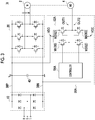
- Fig. 3 is a circuit diagram of a circuit 1A related to Example 1.
- the rectifier 10 is a diode bridge circuit
- the inverter 20 is a three-phase inverter.
- a full-bridge circuit 52A includes a first transistor pair 60 and a second transistor pair 62.
- the first transistor pair 60 includes two transistors M1 and M4 diagonally provided, and the second transistor pair 62 includes two transistors M2 and M3 diagonally provided.
- an insulated gate bipolar transistor (IGBT), a bipolar transistor, or a metal oxide semiconductor field effect transistor (MOSFET) may be used.
- a controller 54A controls the four transistors M1 to M4 of the full-bridge circuit 52A.
- a diode is inversely connected in parallel to each of the transistors M1 to M4.
- Fig. 4 is a waveform diagram illustrating a first braking operation performed by a drive circuit 50A in Fig. 3 .
- Fig. 4 illustrates a time average of the drive voltage V DRV , a state of each transistor of the full-bridge circuit 52A, and a current I MB flowing through the excitation coil of the electromagnetic brake 4 in order from the top.
- An operation of the drive circuit 50 is started at time point t0.
- the first transistor pair 60 (M1 and M4) of the full-bridge circuit 52 is fixed to an ON state, and the transistors M2 and M3 of the second transistor pair 62 are fixed to an OFF state.
- the drive voltage V DRV at this time is the same as the DC link voltage V DC ( ⁇ 600 V).
- the excitation coil is strongly excited right after the starting, and thus the brake can be rapidly released.
- the transistors M1 and M4 of the first transistor pair 60 perform switching in a state in which the transistors M2 and M3 of the second transistor pair 62 is maintained in an OFF state.
- the coil current I MB flows through the diodes connected in parallel to the transistors M3 and M4.
- DUTY indicates a duty ratio of each of the transistors M1 and M4 of the first transistor pair 60.
- the duty ratio DUTY of switching of the transistors M1 and M4 of the first transistor pair 60 may be adjusted depending on a rated voltage to be applied to the electromagnetic brake 4.
- the duty ratio DUTY may be determined based on a rated value V DRV(SPEC) of the drive voltage V DRV to be applied to the electromagnetic brake 4.
- DUTY V DRV(SPEC) /V DC ⁇ 100%
- the first transistor pair 60 (M1 and M4) may perform switching at a duty ratio DUTY' higher than the duty ratio DUTY in the releasing period T 12 . Consequently, the excitation coil can be strongly excited in the overexcitation period T 01 , and thus the degree of excitation depending on the drive voltage V DRV may be adjusted according to the duty ratio DUTY' .
- V DRV V DC ⁇ DUTY'
- Fig. 5A is a circuit diagram illustrating a state of the full-bridge circuit 52 in the releasing period T 12 .
- the coil current I MB flows from the DC link bus 38P to the DC link bus 38N via the transistor M1, an excitation coil L of the electromagnetic brake 4, and the transistor M4.
- a braking period T 23 is started, both of the transistors M1 and M4 of the first transistor pair 60 are turned off, and the transistors M2 and M3 of the second transistor pair 62 are fixed to an ON state.
- a voltage of 0 V appears in the terminal OUT1
- the voltage V DC appears in the terminal OUT2.
- a voltage applied to the excitation coil is -V DC with a polarity opposite to the voltage in the releasing period.
- the voltage -V DC with the opposite polarity acts to attenuate the coil current I MB .
- Fig. 5B is a circuit diagram illustrating a state of the full-bridge circuit 52 in the braking period T 23 .
- the coil current I MB returns from the DC link bus 38N to the DC link bus 38P via the transistor M3, the excitation coil L of the electromagnetic brake 4, and the transistor M2, and can thus be accumulated as electric charge in the DC link capacitor 40.
- the electromagnetic brake 4 is brought into a holding state.
- the coil current I MB does not return to the excitation coil in the braking period T 23 .
- Fig. 6 is a waveform diagram illustrating a second braking operation performed by the drive circuit 50A in Fig. 3 .
- the second transistor pair 62 performs switching in the braking period T 23 .
- the coil current I MB flows through the diodes connected in parallel to the transistors M2 and M4.
- the first transistor pair 60 may be fixed to an OFF state, one of the transistors M2 and M3 of the second transistor pair 62 may be fixed to an ON state, and the other transistor may perform switching.
- an attenuation rate of the coil current I MB can be adjusted depending on a duty ratio (an ON time ratio) of the second transistor pair 62.
- the first transistor pair 60 and the second transistor pair 62 may perform switching in a complementary manner. According to the braking operation, an attenuation rate of the coil current I MB can be adjusted depending on a time ratio between a period in which the first transistor pair 60 is turned on and the second transistor pair 62 is turned on.
- the transistors M1 and M3 forming a leg on opposite side to a leg including one transistor M2 may perform switching in a complementary manner in a state in which one transistor M2 of the second transistor pair 62 is fixed to an ON state.
- an attenuation rate of the coil current I MB can be adjusted depending on a duty ratio of the transistors M1 and M3 (or M2 and M4) forming an opposite side leg.
- the transistors M2 and M4 forming a leg on opposite side to a leg including one transistor M3 may perform switching in a complementary manner in a state in which one transistor M3 of the second transistor pair 62 is fixed to an ON state.
- the braking period T 23 (i) a period in which the coil current I MB flows through the transistor M3, the excitation coil L, and the transistor M2 and (ii) a period in which the coil current I MB flows through a lower loop including the transistor M3, the excitation coil L, and the transistor M4 are alternately repeated.
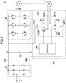
- Fig. 7 is a circuit diagram illustrating a drive circuit 50B related to Modification Example 1.
- a full-bridge circuit 52B of the drive circuit 50B includes a diode pair 64 having two diodes D2 and D3 instead of the second transistor pair 62 (M2 and M3) in Figs. 5A and 5B .
- the transistors M1 and M4 are turned off.
- An operation of the drive circuit 50B is the same as the first braking operation in Fig. 4 .
- the overexcitation period T 01 in Fig. 4 may be omitted.
- the transistors M1 and M4 may be fixed to an ON state (duty ratio of 100%).
- the present invention is applicable to brake control.
Landscapes
- Engineering & Computer Science (AREA)
- Power Engineering (AREA)
- General Engineering & Computer Science (AREA)
- Mechanical Engineering (AREA)
- Stopping Of Electric Motors (AREA)
- Inverter Devices (AREA)
Abstract
Description
- The present invention relates to a brake drive circuit.
- An electromagnetic brake is widely used as means for stopping rotation of a motor. The electromagnetic brake is an example of a mechanical brake. In a non-excitation operation type electromagnetic brake, in a state in which a current does not flow through an excitation coil, an armature is pressed against a brake hub by a spring coil, and the brake is brought into a working state (holding state). In a case where a voltage is applied to the excitation coil, an electromagnet sucks the armature, and thus the brake is brought into a releasing state. Based on such characteristics, the non-excitation operation type electromagnetic brake is frequently used for an application in which safety is to be prioritized in an emergency or at the time of power failure.
- As drive circuits for an electromagnetic brake, there are a normal braking circuit and a sudden braking circuit.
Fig. 1 is a circuit diagram of a normal braking circuit. Arectifier 10 rectifies an AC voltage. Aninverter 20 converts a DC voltage VDC generated by therectifier 10 into an AC voltage, and thus drives amotor 2. - A
normal braking circuit 30 includes aswitch 32, aswitch 34, and a half-wave rectifier 36. An AC voltage is applied to thenormal braking circuit 30. Theswitches electromagnetic brake 4 via the half-wave rectifier 36. - The two
switches electromagnetic brake 4 is brought into a holding state. In a case where theswitches electromagnetic brake 4 hitherto flows in a loop formed by the excitation coil and a diode D2 and attenuates at a certain time constant. In a case where the coil current is smaller than a sucking/holding current, theelectromagnetic brake 4 is brought into a holding state, and slow attenuation of the coil current is a delay before the braking is performed. - An operation in an open state of the sudden braking circuit is the same as that of the normal braking circuit, and a voltage obtained through half-wave rectification is applied to the excitation coil. The sudden braking circuit has a configuration in which conduction of the excitation coil is stopped, and then a coil current flow to another path not to return to the excitation coil, when the
electromagnetic brake 4 is brought into a holding state. -
- [PTL 1] Japanese Unexamined Utility Model Publication No.
4-111293 - [PTL 2] Japanese Unexamined Patent Publication No.
2001-349358 - The present invention has been made in consideration of the circumstances, and an exemplary object of aspects thereof is to provide a novel brake drive circuit capable of suddenly braking an electromagnetic brake.
- An aspect of the present invention relates to a drive circuit for an electromagnetic brake used in a circuit including a motor, a converter converting an AC voltage into a DC voltage to be generated between a pair of DC link buses, and an inverter converting the DC voltage into an AC voltage and driving the motor. The drive circuit includes a full-bridge circuit that has a pair of power supply terminals connected to the pair of DC link buses, and a pair of output terminals connected to the electromagnetic brake.
- According to the aspect, the electromagnetic brake can be released by applying a drive voltage corresponding to a DC voltage at the pair of DC link buses thereto via the full-bridge circuit. In a holding state, application of the drive voltage to the electromagnetic brake via the full-bridge circuit is stopped, a current flowing through the excitation coil of the electromagnetic brake via the full-bridge circuit is returned to the DC link buses, and thus sudden braking is possible. The current in the excitation coil is not consumed in a resistor or the like, and is recovered to the DC link buses so as to be reused, and is thus excellent from the viewpoint of energy saving.
- The full-bridge circuit may include a first transistor pair including two transistors provided diagonally and a second transistor pair including two transistors provided diagonally.
- The full-bridge circuit may include a first transistor pair including two transistors provided diagonally and a diode pair including two diodes provided diagonally.
- In a releasing state of the electromagnetic brake, a duty ratio of switching of the first transistor pair may be adjustable depending on a drive voltage to be applied to the electromagnetic brake. Consequently, it is possible to increase the degree of freedom of selection of an electromagnetic brake.
- In an overexcitation period after starting, the first transistor pair (i) may be fixed to an ON state or (ii) may perform switching at a duty ratio higher than a duty ratio of switching of the first transistor pair in a releasing period after the overexcitation period.
- In a braking period, the second transistor pair of the full-bridge circuit may be fixed to an ON state.
- In a braking period, at least one of the two transistors of the second transistor pair of the full-bridge circuit may perform switching. Consequently, an amount of a current recovered to the DC link buses can be restricted or adjusted.
- A method, an apparatus, and a system replacing any combination of the constituent elements or a constituent element or an expression of the process are also effective as aspects of the present invention.
- The disclosure in this section (Solution to Problem) does not explain all the essential features of the present invention, and, therefore, the sub-combinations of the features described may also fall within the present invention.
- According to the aspect of the present invention, it is possible to suddenly brake an electromagnetic brake.
-
-
Fig. 1 is a circuit diagram of a normal braking circuit. -
Fig. 2 is a block diagram of a circuit including a drive circuit according to an embodiment. -
Fig. 3 is a circuit diagram of a circuit related to Example 1. -
Fig. 4 is a waveform diagram illustrating a first braking operation performed by a drive circuit inFig. 3 . -
Figs. 5A and 5B are circuit diagrams illustrating states of a full-bridge circuit in a releasing period and a braking period. -
Fig. 6 is a waveform diagram illustrating a second braking operation performed by a drive circuit inFig. 3 . -
Fig. 7 is a circuit diagram of a drive circuit related to Modification Example 1. - Hereinafter, an embodiment of the invention will be described with reference to the drawings. Throughout the drawings, like or equivalent constituent elements, members, and processes are given the like reference numerals, and repeated description will be omitted as appropriate. The embodiment is not intended to limit the invention and is only an example, and all features described in the embodiment and combinations thereof cannot be said to be essential elements of the invention.
-
Fig. 2 is a block diagram of a circuit (system) 1 including adrive circuit 50 according to an embodiment. The circuit 1 includes amotor 2, anelectromagnetic brake 4, arectifier 10, aninverter 20,DC link buses DC link capacitor 40, and thedrive circuit 50. - The
rectifier 10 converts an AC voltage VAC into a DC voltage (referred to as DC link voltage) VDC, and generates the DC link voltage between a pair of theDC link buses DC link capacitor 40 is connected between theDC link buses inverter 20 converts the DC link voltage VDC into AC voltages VU to VW, and thus drives themotor 2. - The
drive circuit 50 includes a full-bridge circuit (H bridge circuit) 52 and acontroller 54. The full-bridge circuit 52 has a pair of power supply terminals VDD and VSS connected to the pair of DC link buses 38, and a pair of output terminals OUT1 and OUT2 connected to theelectromagnetic brake 4. The full-bridge circuit 52 includes four elements between the terminals VDD and OUT1, between the terminals VDD and OUT2, between the terminals VSS and OUT1, and between the terminals VSS and OUT2. As will be described later, the full-bridge circuit 52 is configured with a combination of switch elements or a combination of a switch element and a rectification element. - Next, a description will be made of control of the full-
bridge circuit 52 in thecontroller 54 and an operation of thedrive circuit 50. - The
controller 54 controls a state of the full-bridge circuit 52, so as to switch between a releasing state and a holding state of theelectromagnetic brake 4. Specifically, thecontroller 54 brings the full-bridge circuit 52 into an active state, and thus generates a drive voltage VDRV corresponding to the DC link voltage VDC between the pair ofDC link buses bridge circuit 52. In a case where the drive voltage VDRV is applied to theelectromagnetic brake 4, theelectromagnetic brake 4 is brought into a releasing state. - In a holding state, the
controller 54 brings the full-bridge circuit 52 into an inactive state, and thus brings the outputs OUT1 and OUT2 into a high impedance state in a fixed manner or a time division manner. Consequently, application of the forward drive voltage VDRV to theelectromagnetic brake 4 is stopped. A current flowing through the excitation coil of theelectromagnetic brake 4 is recovered to the DC link buses via the full-bridge circuit 52 without returning to the excitation coil. Consequently, sudden braking becomes possible. - The current in the excitation coil is not consumed in a resistor or the like, and is recovered to the
DC link buses - The present invention covers various devices and circuits derived from the block diagram or the circuit diagram of
Fig. 2 or the above description, and is not limited to a specific configuration. Hereinafter, more specific Examples or modification examples will be described not to limit the scope of the present invention but to help with and to clarify the understanding of the nature of the invention or a circuit operation. -
Fig. 3 is a circuit diagram of acircuit 1A related to Example 1. In the present example, therectifier 10 is a diode bridge circuit, and theinverter 20 is a three-phase inverter. - A full-
bridge circuit 52A includes afirst transistor pair 60 and asecond transistor pair 62. Thefirst transistor pair 60 includes two transistors M1 and M4 diagonally provided, and thesecond transistor pair 62 includes two transistors M2 and M3 diagonally provided. As the transistors M1 to M4, an insulated gate bipolar transistor (IGBT), a bipolar transistor, or a metal oxide semiconductor field effect transistor (MOSFET) may be used. Acontroller 54A controls the four transistors M1 to M4 of the full-bridge circuit 52A. A diode is inversely connected in parallel to each of the transistors M1 to M4. -
Fig. 4 is a waveform diagram illustrating a first braking operation performed by adrive circuit 50A inFig. 3 .Fig. 4 illustrates a time average of the drive voltage VDRV, a state of each transistor of the full-bridge circuit 52A, and a current IMB flowing through the excitation coil of theelectromagnetic brake 4 in order from the top. - An operation of the
drive circuit 50 is started at time point t0. In an overexcitation period T01 right after the operation is started, the first transistor pair 60 (M1 and M4) of the full-bridge circuit 52 is fixed to an ON state, and the transistors M2 and M3 of thesecond transistor pair 62 are fixed to an OFF state. The drive voltage VDRV at this time is the same as the DC link voltage VDC (≅ 600 V). The excitation coil is strongly excited right after the starting, and thus the brake can be rapidly released. - In the subsequent releasing period T12, the transistors M1 and M4 of the
first transistor pair 60 perform switching in a state in which the transistors M2 and M3 of thesecond transistor pair 62 is maintained in an OFF state. In a period in which thefirst transistor pair 60 is in an OFF state, the coil current IMB flows through the diodes connected in parallel to the transistors M3 and M4. - The drive voltage VDRV (average) in the releasing period T12 is VDRV = VDC × DUTY. DUTY indicates a duty ratio of each of the transistors M1 and M4 of the
first transistor pair 60. In the releasing period T12, the duty ratio DUTY of switching of the transistors M1 and M4 of thefirst transistor pair 60 may be adjusted depending on a rated voltage to be applied to theelectromagnetic brake 4. The duty ratio DUTY may be determined based on a rated value VDRV(SPEC) of the drive voltage VDRV to be applied to theelectromagnetic brake 4. DUTY = VDRV(SPEC)/VDC × 100% - In the overexcitation period T01, the first transistor pair 60 (M1 and M4) may perform switching at a duty ratio DUTY' higher than the duty ratio DUTY in the releasing period T12. Consequently, the excitation coil can be strongly excited in the overexcitation period T01, and thus the degree of excitation depending on the drive voltage VDRV may be adjusted according to the duty ratio DUTY' . VDRV = VDC × DUTY'
-
Fig. 5A is a circuit diagram illustrating a state of the full-bridge circuit 52 in the releasing period T12. The coil current IMB flows from theDC link bus 38P to theDC link bus 38N via the transistor M1, an excitation coil L of theelectromagnetic brake 4, and the transistor M4. - In a case where a command for brake holding is input to the
controller 54 at time point t2, a braking period T23 is started, both of the transistors M1 and M4 of thefirst transistor pair 60 are turned off, and the transistors M2 and M3 of thesecond transistor pair 62 are fixed to an ON state. In this case, a voltage of 0 V appears in the terminal OUT1, and the voltage VDC appears in the terminal OUT2. In other words, a voltage applied to the excitation coil is -VDC with a polarity opposite to the voltage in the releasing period. The voltage -VDC with the opposite polarity acts to attenuate the coil current IMB. -
Fig. 5B is a circuit diagram illustrating a state of the full-bridge circuit 52 in the braking period T23. The coil current IMB returns from theDC link bus 38N to theDC link bus 38P via the transistor M3, the excitation coil L of theelectromagnetic brake 4, and the transistor M2, and can thus be accumulated as electric charge in theDC link capacitor 40. In a case where the coil current IMB is smaller than a sucking/holding current, theelectromagnetic brake 4 is brought into a holding state. - In a case where the coil current IMB is reduced to about zero, the transistors M1 to M4 are all turned off, and thus a non-excitation period T34 occurs.
- In the first braking operation, the coil current IMB does not return to the excitation coil in the braking period T23.
-
Fig. 6 is a waveform diagram illustrating a second braking operation performed by thedrive circuit 50A inFig. 3 . In the second braking operation, thesecond transistor pair 62 performs switching in the braking period T23. In a period in which the transistors M2 and M4 of thesecond transistor pair 62 are turned off, the coil current IMB flows through the diodes connected in parallel to the transistors M2 and M4. - According to this braking operation, a voltage generated between both ends of the excitation coil in the braking period T23 according to a duty ratio (an ON time ratio) of the
second transistor pair 62, and thus an attenuation rate of the coil current IMB can be adjusted. - In the braking period T23 in
Fig. 4 , thefirst transistor pair 60 may be fixed to an OFF state, one of the transistors M2 and M3 of thesecond transistor pair 62 may be fixed to an ON state, and the other transistor may perform switching. According to the braking operation, an attenuation rate of the coil current IMB can be adjusted depending on a duty ratio (an ON time ratio) of thesecond transistor pair 62. - In the braking period T23 in
Fig. 4 , thefirst transistor pair 60 and thesecond transistor pair 62 may perform switching in a complementary manner. According to the braking operation, an attenuation rate of the coil current IMB can be adjusted depending on a time ratio between a period in which thefirst transistor pair 60 is turned on and thesecond transistor pair 62 is turned on. - In the braking period T23 in
Fig. 4 , the transistors M1 and M3 forming a leg on opposite side to a leg including one transistor M2 may perform switching in a complementary manner in a state in which one transistor M2 of thesecond transistor pair 62 is fixed to an ON state. - In the braking operation, in the braking period T23, (i) a period in which the coil current IMB flows through the transistor M3, the excitation coil L, and the transistor M2 and (ii) a period in which the coil current IMB flows through an upper loop including the transistor M1, the excitation coil L, and the transistor M2 are alternately repeated.
- According to the braking operation, an attenuation rate of the coil current IMB can be adjusted depending on a duty ratio of the transistors M1 and M3 (or M2 and M4) forming an opposite side leg.
- The transistors M2 and M4 forming a leg on opposite side to a leg including one transistor M3 may perform switching in a complementary manner in a state in which one transistor M3 of the
second transistor pair 62 is fixed to an ON state. In this case, in the braking period T23, (i) a period in which the coil current IMB flows through the transistor M3, the excitation coil L, and the transistor M2 and (ii) a period in which the coil current IMB flows through a lower loop including the transistor M3, the excitation coil L, and the transistor M4 are alternately repeated. - As mentioned above, the present invention has been described based on the embodiment. The embodiment is only an example, and it is understood by a person skilled in the art that various modification examples may occur in combinations of the respective constituent elements or respective processing processes, and the modification examples are also included in the scope of the present invention. Hereinafter, such modification examples will be described.
-
Fig. 7 is a circuit diagram illustrating adrive circuit 50B related to Modification Example 1. A full-bridge circuit 52B of thedrive circuit 50B includes adiode pair 64 having two diodes D2 and D3 instead of the second transistor pair 62 (M2 and M3) inFigs. 5A and 5B . In the braking period T23, the transistors M1 and M4 are turned off. An operation of thedrive circuit 50B is the same as the first braking operation inFig. 4 . - The overexcitation period T01 in
Fig. 4 may be omitted. Alternatively, in the releasing period T12, the transistors M1 and M4 may be fixed to an ON state (duty ratio of 100%). - The present invention has been described by using specific words and phrases based on the embodiment, but the embodiment merely represents one aspect of the principles or applications of the present invention, and it is considered that various modification examples or disposition changes may occur in the embodiment within the scope without departing from the concept of the present invention.
-
- 1
- CIRCUIT
- 2
- MOTOR
- 4
- ELECTROMAGNETIC BRAKE
- 10
- RECTIFIER
- 20
- INVERTER
- 30
- NORMAL BRAKING CIRCUIT
- 32 AND 34
- SWITCH
- 36
- HALF-WAVE RECTIFIER
- 38
- DC LINK BUS
- 40
- DC LINK CAPACITOR
- 50
- DRIVE CIRCUIT
- VDD AND VSS
- POWER SUPPLY TERMINAL
- OUT1 AND OUT2
- OUTPUT TERMINAL
- 52
- FULL-BRIDGE CIRCUIT
- 54
- CONTROLLER
- M1, M2, M3, AND M4
- TRANSISTOR
- 60
- FIRST TRANSISTOR PAIR
- 62
- SECOND TRANSISTOR PAIR
- 64
- DIODE PAIR
- D1 AND D2
- DIODE
- The present invention is applicable to brake control.
Claims (7)
- A drive circuit for an electromagnetic brake used in a circuit including a motor, a converter converting an AC voltage into a DC voltage to be generated between a pair of DC link buses, and an inverter converting the DC voltage into an AC voltage and driving the motor, the drive circuit comprising:
a full-bridge circuit that has a pair of power supply terminals connected to the pair of DC link buses, and a pair of output terminals connected to the electromagnetic brake. - The drive circuit according to claim 1,
wherein the full-bridge circuit includes a first transistor pair including two transistors provided diagonally and a second transistor pair including two transistors provided diagonally. - The drive circuit according to claim 1,
wherein the full-bridge circuit includes a first transistor pair including two transistors provided diagonally and a diode pair including two diodes provided diagonally. - The drive circuit according to claim 2 or 3,
wherein, in a releasing state of the electromagnetic brake, a duty ratio of switching of the first transistor pair is adjustable depending on a voltage to be applied to the electromagnetic brake. - The drive circuit according to any one of claims 2 to 4,
wherein, in an overexcitation period after starting, the first transistor pair (i) is fixed to an ON state or (ii) performs switching at a duty ratio higher than a duty ratio of switching of the first transistor pair in a releasing period after the overexcitation period. - The drive circuit according to claim 2,
wherein, in a braking period, the second transistor pair of the full-bridge circuit is fixed to an ON state. - The drive circuit according to claim 2,
wherein, in a braking period, at least one of the two transistors of the second transistor pair of the full-bridge circuit performs switching.
Applications Claiming Priority (2)
| Application Number | Priority Date | Filing Date | Title |
|---|---|---|---|
| JP2017018173A JP6814060B2 (en) | 2017-02-03 | 2017-02-03 | Brake drive circuit |
| PCT/JP2018/002932 WO2018143182A1 (en) | 2017-02-03 | 2018-01-30 | Brake drive circuit |
Publications (2)
| Publication Number | Publication Date |
|---|---|
| EP3579398A1 true EP3579398A1 (en) | 2019-12-11 |
| EP3579398A4 EP3579398A4 (en) | 2019-12-11 |
Family
ID=63040684
Family Applications (1)
| Application Number | Title | Priority Date | Filing Date |
|---|---|---|---|
| EP18747830.0A Withdrawn EP3579398A4 (en) | 2017-02-03 | 2018-01-30 | BRAKE CONTROL CIRCUIT |
Country Status (5)
| Country | Link |
|---|---|
| US (1) | US11005391B2 (en) |
| EP (1) | EP3579398A4 (en) |
| JP (1) | JP6814060B2 (en) |
| CN (1) | CN110226284A (en) |
| WO (1) | WO2018143182A1 (en) |
Families Citing this family (9)
| Publication number | Priority date | Publication date | Assignee | Title |
|---|---|---|---|---|
| EP3508552A1 (en) | 2018-01-05 | 2019-07-10 | Castrol Limited | Phase change material for heat exchange fluid/coolant |
| GB201905733D0 (en) | 2019-04-24 | 2019-06-05 | Bp Plc | Dielectric thermal managment fluids and methods for using them |
| JP7445486B2 (en) * | 2020-03-26 | 2024-03-07 | 住友重機械工業株式会社 | Brake drive circuit and electromagnetic brake system |
| WO2021193456A1 (en) * | 2020-03-26 | 2021-09-30 | 住友重機械工業株式会社 | Drive circuit for inductive load and electromagnetic brake system |
| JP7445485B2 (en) * | 2020-03-26 | 2024-03-07 | 住友重機械工業株式会社 | Inductive load drive circuit and electromagnetic brake system |
| JP2021166455A (en) * | 2020-04-08 | 2021-10-14 | 株式会社ミツバ | Electric motor and manufacturing method of electric motor |
| CN111864717B (en) * | 2020-08-14 | 2025-07-15 | 精进电动科技股份有限公司 | Electromagnetic clutch circuit and automobile |
| JP7761642B2 (en) * | 2021-05-19 | 2025-10-28 | 住友重機械工業株式会社 | Electromagnetic brake control device, electromagnetic brake control method, electromagnetic brake control program, and electromagnetic control device |
| JP7799081B2 (en) * | 2022-11-04 | 2026-01-14 | ファナック株式会社 | Brake drive device that drives a mechanical brake device |
Family Cites Families (18)
| Publication number | Priority date | Publication date | Assignee | Title |
|---|---|---|---|---|
| JPS57202899A (en) * | 1981-06-08 | 1982-12-11 | Ogura Clutch Co Ltd | Control circuit for electromagnetic clutch and brake |
| JP2566759B2 (en) * | 1986-06-24 | 1996-12-25 | 三木プ−リ株式会社 | Coil control circuit for magnetic clutches, brakes, etc. |
| JPH04111293U (en) | 1991-03-18 | 1992-09-28 | 日本サーボ株式会社 | Brake drive circuit |
| JP2808937B2 (en) * | 1991-08-07 | 1998-10-08 | 神鋼電機株式会社 | Electromagnetic clutch and electromagnetic brake torque control device |
| JPH07328966A (en) * | 1994-06-07 | 1995-12-19 | Fanuc Ltd | Brake control system for robot |
| JP3416795B2 (en) * | 1998-06-30 | 2003-06-16 | ミネベア株式会社 | Power supply method and device for electromagnetic equipment |
| JP2001349358A (en) | 2000-06-02 | 2001-12-21 | Oriental Motor Co Ltd | Rectifier circuit for electromagnetic brake |
| TW200417129A (en) * | 2002-09-04 | 2004-09-01 | Sanki Kk | Excitation controller for a non-excitation actuating brake |
| FR2860108B1 (en) | 2003-09-24 | 2007-01-19 | Johnson Contr Automotive Elect | SYNCHRONOUS RECTIFIER DEVICE AND SYNCHRONOUS ELECTRIC MACHINE USING THE DEVICE |
| JP4811952B2 (en) * | 2006-12-28 | 2011-11-09 | 株式会社ハーモニック・ドライブ・システムズ | Non-excitation electromagnetic brake |
| JP2009083710A (en) * | 2007-10-01 | 2009-04-23 | Renesas Technology Corp | Motor controller and electric vehicle |
| FI120938B (en) * | 2009-02-06 | 2010-05-14 | Kone Corp | Arrangement and method of controlling the lift brake |
| JP5192430B2 (en) | 2009-03-24 | 2013-05-08 | 平田機工株式会社 | Control apparatus and control method |
| CN102664579B (en) * | 2012-04-17 | 2014-10-15 | 燕山大学 | Control device of electromagnetic brake |
| US8804376B2 (en) * | 2012-06-26 | 2014-08-12 | Cyber Power Systems Inc. | DC/DC converter with selectable coupling ratio and power inverter using the same |
| JP2014192919A (en) * | 2013-03-26 | 2014-10-06 | Seiko Epson Corp | Motor drive and electronic apparatus |
| EP3006385B1 (en) * | 2014-10-09 | 2017-05-31 | Kone Corporation | A brake controller and an elevator system |
| JP2018074794A (en) * | 2016-10-31 | 2018-05-10 | ファナック株式会社 | Motor drive device with common forward converter |
-
2017
- 2017-02-03 JP JP2017018173A patent/JP6814060B2/en active Active
-
2018
- 2018-01-30 CN CN201880008519.0A patent/CN110226284A/en active Pending
- 2018-01-30 WO PCT/JP2018/002932 patent/WO2018143182A1/en not_active Ceased
- 2018-01-30 EP EP18747830.0A patent/EP3579398A4/en not_active Withdrawn
-
2019
- 2019-07-29 US US16/525,155 patent/US11005391B2/en not_active Expired - Fee Related
Also Published As
| Publication number | Publication date |
|---|---|
| EP3579398A4 (en) | 2019-12-11 |
| US20190356240A1 (en) | 2019-11-21 |
| CN110226284A (en) | 2019-09-10 |
| WO2018143182A1 (en) | 2018-08-09 |
| JP6814060B2 (en) | 2021-01-13 |
| US11005391B2 (en) | 2021-05-11 |
| JP2018126017A (en) | 2018-08-09 |
Similar Documents
| Publication | Publication Date | Title |
|---|---|---|
| US11005391B2 (en) | Brake drive circuit | |
| CN110383677B (en) | Motor drive device and refrigeration cycle applicable equipment | |
| US9680389B2 (en) | Power conversion device | |
| CN110784154B (en) | Motor drive device | |
| CN101663219B (en) | Brake control device for elevator | |
| CN106865371B (en) | Elevator brake and its control method | |
| KR101690000B1 (en) | Electric motor with brake | |
| TW202211594A (en) | Motor control apparatus and method of controlling the same | |
| JP2014183702A (en) | Electric power conversion system | |
| CN112715002A (en) | Control device for an inverter, inverter for an asynchronous machine, vehicle and method for operating an inverter | |
| JP7445486B2 (en) | Brake drive circuit and electromagnetic brake system | |
| JPWO2006016400A1 (en) | DC voltage drive type magnet contactor drive circuit and power converter | |
| JP5976953B2 (en) | Bridge leg | |
| CN106464151A (en) | Apparatus for operating rectifier, particularly half-controlled rectifier bridge, and method for operating rectifier | |
| US20150280583A1 (en) | Bidirectional switched mode power supply | |
| TWI825399B (en) | Inductive load drive circuit and electromagnetic braking system | |
| US10298218B2 (en) | Method and device for controlling an electrical or electronic switching element | |
| US20250079971A1 (en) | Gate drive circuit and power conversion device | |
| CN104882878B (en) | The method of the safety-related disconnection of the power-supply system and DC driven of DC driven | |
| JP6396562B1 (en) | Lifting magnet control system | |
| JP7761642B2 (en) | Electromagnetic brake control device, electromagnetic brake control method, electromagnetic brake control program, and electromagnetic control device | |
| CN111030512A (en) | Control system and control method for dynamic braking of motor | |
| US20240297604A1 (en) | Device for the de-excitation of at least one rotor winding of a synchronous motor, synchronous motor, method for operating a synchronous motor, motor vehicle | |
| KR0179761B1 (en) | Elevator Motor Protection Circuit | |
| JP7445485B2 (en) | Inductive load drive circuit and electromagnetic brake system |
Legal Events
| Date | Code | Title | Description |
|---|---|---|---|
| STAA | Information on the status of an ep patent application or granted ep patent |
Free format text: STATUS: THE INTERNATIONAL PUBLICATION HAS BEEN MADE |
|
| PUAI | Public reference made under article 153(3) epc to a published international application that has entered the european phase |
Free format text: ORIGINAL CODE: 0009012 |
|
| STAA | Information on the status of an ep patent application or granted ep patent |
Free format text: STATUS: REQUEST FOR EXAMINATION WAS MADE |
|
| STAA | Information on the status of an ep patent application or granted ep patent |
Free format text: STATUS: EXAMINATION IS IN PROGRESS |
|
| 17P | Request for examination filed |
Effective date: 20190722 |
|
| A4 | Supplementary search report drawn up and despatched |
Effective date: 20191002 |
|
| AK | Designated contracting states |
Kind code of ref document: A1 Designated state(s): AL AT BE BG CH CY CZ DE DK EE ES FI FR GB GR HR HU IE IS IT LI LT LU LV MC MK MT NL NO PL PT RO RS SE SI SK SM TR |
|
| AX | Request for extension of the european patent |
Extension state: BA ME |
|
| 17Q | First examination report despatched |
Effective date: 20191121 |
|
| DAV | Request for validation of the european patent (deleted) | ||
| DAX | Request for extension of the european patent (deleted) | ||
| STAA | Information on the status of an ep patent application or granted ep patent |
Free format text: STATUS: THE APPLICATION IS DEEMED TO BE WITHDRAWN |
|
| 18D | Application deemed to be withdrawn |
Effective date: 20250108 |