EP3579000A1 - Power monitor - Google Patents
Power monitor Download PDFInfo
- Publication number
- EP3579000A1 EP3579000A1 EP19178379.4A EP19178379A EP3579000A1 EP 3579000 A1 EP3579000 A1 EP 3579000A1 EP 19178379 A EP19178379 A EP 19178379A EP 3579000 A1 EP3579000 A1 EP 3579000A1
- Authority
- EP
- European Patent Office
- Prior art keywords
- circuit
- processing circuit
- abnormal
- predetermined
- power
- Prior art date
- Legal status (The legal status is an assumption and is not a legal conclusion. Google has not performed a legal analysis and makes no representation as to the accuracy of the status listed.)
- Granted
Links
Images


Classifications
-
- G—PHYSICS
- G06—COMPUTING OR CALCULATING; COUNTING
- G06F—ELECTRIC DIGITAL DATA PROCESSING
- G06F1/00—Details not covered by groups G06F3/00 - G06F13/00 and G06F21/00
- G06F1/26—Power supply means, e.g. regulation thereof
- G06F1/32—Means for saving power
- G06F1/3203—Power management, i.e. event-based initiation of a power-saving mode
- G06F1/3206—Monitoring of events, devices or parameters that trigger a change in power modality
-
- G—PHYSICS
- G01—MEASURING; TESTING
- G01R—MEASURING ELECTRIC VARIABLES; MEASURING MAGNETIC VARIABLES
- G01R19/00—Arrangements for measuring currents or voltages or for indicating presence or sign thereof
- G01R19/0084—Measuring voltage only
-
- G—PHYSICS
- G01—MEASURING; TESTING
- G01R—MEASURING ELECTRIC VARIABLES; MEASURING MAGNETIC VARIABLES
- G01R31/00—Arrangements for testing electric properties; Arrangements for locating electric faults; Arrangements for electrical testing characterised by what is being tested not provided for elsewhere
- G01R31/28—Testing of electronic circuits, e.g. by signal tracer
- G01R31/2851—Testing of integrated circuits [IC]
-
- G—PHYSICS
- G01—MEASURING; TESTING
- G01R—MEASURING ELECTRIC VARIABLES; MEASURING MAGNETIC VARIABLES
- G01R31/00—Arrangements for testing electric properties; Arrangements for locating electric faults; Arrangements for electrical testing characterised by what is being tested not provided for elsewhere
- G01R31/40—Testing power supplies
-
- H—ELECTRICITY
- H03—ELECTRONIC CIRCUITRY
- H03K—PULSE TECHNIQUE
- H03K7/00—Modulating pulses with a continuously-variable modulating signal
- H03K7/08—Duration or width modulation ; Duty cycle modulation
-
- H—ELECTRICITY
- H02—GENERATION; CONVERSION OR DISTRIBUTION OF ELECTRIC POWER
- H02M—APPARATUS FOR CONVERSION BETWEEN AC AND AC, BETWEEN AC AND DC, OR BETWEEN DC AND DC, AND FOR USE WITH MAINS OR SIMILAR POWER SUPPLY SYSTEMS; CONVERSION OF DC OR AC INPUT POWER INTO SURGE OUTPUT POWER; CONTROL OR REGULATION THEREOF
- H02M3/00—Conversion of DC power input into DC power output
- H02M3/22—Conversion of DC power input into DC power output with intermediate conversion into AC
- H02M3/24—Conversion of DC power input into DC power output with intermediate conversion into AC by static converters
- H02M3/28—Conversion of DC power input into DC power output with intermediate conversion into AC by static converters using discharge tubes with control electrode or semiconductor devices with control electrode to produce the intermediate AC
- H02M3/325—Conversion of DC power input into DC power output with intermediate conversion into AC by static converters using discharge tubes with control electrode or semiconductor devices with control electrode to produce the intermediate AC using devices of a triode or a transistor type requiring continuous application of a control signal
- H02M3/335—Conversion of DC power input into DC power output with intermediate conversion into AC by static converters using discharge tubes with control electrode or semiconductor devices with control electrode to produce the intermediate AC using devices of a triode or a transistor type requiring continuous application of a control signal using semiconductor devices only
- H02M3/33507—Conversion of DC power input into DC power output with intermediate conversion into AC by static converters using discharge tubes with control electrode or semiconductor devices with control electrode to produce the intermediate AC using devices of a triode or a transistor type requiring continuous application of a control signal using semiconductor devices only with automatic control of the output voltage or current, e.g. flyback converters
- H02M3/33523—Conversion of DC power input into DC power output with intermediate conversion into AC by static converters using discharge tubes with control electrode or semiconductor devices with control electrode to produce the intermediate AC using devices of a triode or a transistor type requiring continuous application of a control signal using semiconductor devices only with automatic control of the output voltage or current, e.g. flyback converters with galvanic isolation between input and output of both the power stage and the feedback loop
Definitions
- the present invention relates to a monitor device. More particularly, the present invention relates to an intelligence power monitor.
- a conventional power supply device For preventing the power from being abnormal or to prevent the power failure of the power from being occurred, a conventional power supply device has two power supplies. When any one of the power supplies is abnormal and needs to be repaired, the other one of the power supplies maintains supplying power. Another way is that the conventional power supply device has an uninterruptible power system (UPS). When the power supply device damages or the power failure of the power supply device occurs, the UPS can provide power to machines.
- UPS uninterruptible power system
- the conventional power supply device needs to have two power supplies, and the cost is therefore higher. No matter the conventional power supply device adopts having two power supplies manner or having UPS manner to maintain supplying power, this is a remedy after the conventional power supply device is already damaged or the power failure of the conventional power supply device occurs.
- the loss of the factory cost by the power supply device being damaged or the power failure of the conventional power supply device occurring is extremely high. The loss of the factory is sometimes beyond compute. Therefore, how to reduce the cost of the power supply device, and how to prevent the power supply device from being damaged or to prevent the power failure of the power supply device from occurring is a problem to be improved in the field.
- the power monitor comprises a detecting circuit, a processing circuit, and a warning circuit.
- the detecting circuit detects a first abnormal condition of a primary side circuit and a second abnormal condition of a secondary side circuit.
- the processing circuit calculates a first class and a first occurring number of the first abnormal condition, and calculates a second class and a second occurring number of the second abnormal condition.
- the processing circuit determines whether the first occurring number is larger than a first predetermined number corresponding to the first class; if it is, the processing circuit outputs a first abnormal signal.
- the processing circuit determines whether the second occurring number is larger than a second predetermined number corresponding to the second class; if it is, the processing circuit outputs a second abnormal signal.
- the warning circuit outputs a warning signal according to the first abnormal signal or the second abnormal signal.
- the power monitor comprises a detecting circuit, a processing circuit, and a warning circuit.
- the detecting circuit is configured to detect an input voltage of a primary side circuit of a power converter.
- the processing circuit is configured to compare a condition of the input voltage and a predetermined parameter, wherein if the condition of the input voltage and the predetermined parameter are different, the processing circuit outputs an abnormal signal.
- the warning circuit is configured to output a warning signal according to the abnormal signal.
- Fig. 1 is a circuit block diagram of a power supply device according to some embodiments of the present disclosure.
- the power supply device includes a power converter 100 and a power monitor 200.
- the power monitor 200 includes a detecting circuit 210, a processing circuit 220, a warning circuit 230 and a communication circuit 240.
- the power converter 100 is connected to a power 800 and a load 900.
- the detecting circuit 210 is connected to a primary side circuit 110 of the power converter 100, and connected to a secondary side circuit 120 of the power converter 100.
- the processing circuit 220 is connected to the detecting circuit 210.
- the warning circuit 230 is connected to the processing circuit 220.
- the communication circuit 240 is connected to the warning circuit 230.
- the power converter 100 transforms the energy provided by the power 800, and provides it to the load 900.
- the power 800 can be but not limited to the power grid or other outer power.
- the power monitor 200 is configured to monitor the condition of the power converter 100, and inform users immediately when the power converter 100 is abnormal, so as to prevent the power supply device from being damage/power failure, which will be described in detail as below.
- the detecting circuit 210 of the power monitor 200 detects a first abnormal condition of the primary side circuit 110 of the power converter 100 and a second abnormal condition of the secondary side circuit 120 of the power converter 100 in real time.
- the processing circuit 220 then calculates a first class and a first occurring number of the first abnormal condition, and calculates a second class and a second occurring number of the second abnormal condition. For example, when the energy provided by the power 800 is high, the primary side circuit 110 will receive a high voltage. Meanwhile, the detecting circuit 210 will detect the above-mentioned abnormal condition, and the processing circuit 220 then calculates a class of the abnormal condition (e.g., 1000 volts/750 volts are two kinds of different classes) and a happened number of the abnormal condition.
- a class of the abnormal condition e.g., 1000 volts/750 volts are two kinds of different classes
- an overload condition will happen in the secondary side circuit 120.
- the detecting circuit 210 will detect the above-mentioned abnormal condition, the processing circuit 220 then calculates the class of the abnormal condition (e.g., overload time: 10 seconds/overload time: 3 seconds are two kinds of different classes) and the happened number of the abnormal condition.
- the processing circuit 220 of the power monitor 200 further determines whether a first occurring number is larger than a first predetermined number corresponding to the first class. If it is, the processing circuit 220 outputs a first abnormal signal. Besides, the processing circuit 220 determines whether a second occurring number is larger than a second predetermined number corresponding to the second class. If it is, the processing circuit 220 outputs a second abnormal signal. In one embodiment, the processing circuit 220 receives the first predetermined number corresponding to the first class and the second predetermined number corresponding to the second class from a look-up table.
- the processing circuit 220 receives a related predetermined number according to the class of the abnormal condition of the primary side circuit 110 (e.g., 1000 volts/ 750volts).
- the class of the abnormal condition is 1000 volts
- the damage to the primary side circuit 110 is high due to the abnormal voltage is high. Therefore, the acceptable number of the 1000 volts is predetermined to be 5.
- the processing circuit 220 outputs the abnormal signal.
- the class of the abnormal condition is 750 volts
- the damage to the primary side circuit 110 is low due to the abnormal voltage is low. Therefore, the acceptable number of the 750 volts is predetermined to be 20. If the shock number to the primary side circuit 110 is more than 20, the processing circuit 220 then outputs the abnormal signal.
- the condition of the secondary side circuit 120 is that the processing circuit 220 receives a corresponding predetermined number according to the class of the abnormal condition of the secondary side circuit 120 (e.g., overload time: 10 seconds/overload time: 3 seconds).
- overload time 10 seconds/overload time: 3 seconds.
- the processing circuit 220 outputs the abnormal signal.
- the class of the abnormal condition is that the overload time is 3 seconds
- the damage to the secondary side circuit 120 is low due to the overload time is low. Therefore, the acceptable number of the 3 seconds overload time is predetermined to be 100. If the happened time of the overload condition to the secondary side circuit 120 is more than 100, the processing circuit 220 then outputs the abnormal signal.
- the warning circuit 230 will output a warning signal according to the first abnormal signal corresponding to the primary side circuit 110, or the warning circuit 230 will output the warning signal according to the second abnormal signal corresponding to the secondary side circuit 120.
- the shock number to the primary side circuit 110 by 1000 volts is more than 5
- the damage of elements inside the primary side circuit 110 may achieve the damage tolerance.
- the elements inside the primary side circuit 110 will break down at any time if keep using the elements.
- the warning circuit 230 will output the warning signal, so as to remind users to change the elements inside the primary side circuit 110, in order to avoid damage/power failure of the power supply device.
- the damage of the elements inside the secondary side circuit 120 may achieve the damage tolerance.
- the elements inside the secondary side circuit 120 will break down at any time if keep using the elements.
- the warning circuit 230 will output the warning signal, so as to remind users to change the elements inside the secondary side circuit 120, in order to avoid damage/power failure of the power supply device.
- the abnormal conditions of the primary side circuit 110 and the secondary side circuit 120 of the power converter 100 in the present disclosure are not intended to be limited to the above-mentioned embodiments.
- the abnormal condition of the primary side circuit 110 can also be voltage abnormal, current abnormal, surge or other condition which may damage circuits
- the abnormal condition of the secondary side circuit 120 can also be voltage abnormal, current abnormal, overload or other condition which may damage circuits.
- the power monitor 200 of the present disclosure can be used in remote monitor field.
- the power monitor 200 may include a communication circuit 240. If the primary side circuit 110 or the secondary side circuit 120 of the power converter 100 is abnormal, the communication circuit 240 can be used to transmit the warning signal to a remote monitor system (not shown) through a wired manner or a wireless manner, such that users can monitor the power converters easily in a remote manner. If the abnormal condition happens, staff whose location near the abnormal power converter 100 will be noticed to fix the abnormal power converter 100.
- the power monitor 200 further uses the detecting circuit 210 to detect the primary side circuit 110 or the secondary side circuit 120 of the power converter 100 for generating detection data.
- the communication circuit 240 is further used to transmit detailed detection data (e.g., abnormal condition data) to the remote monitor system.
- the remote monitor system collects all conditions for big data analyzing, and adaptively adjusts the power monitor 200 or the parameter of the look-up table according to analyzing result, such that the power monitor 200 can further monitor and give a waring intelligently.
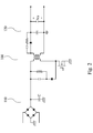
- Fig. 2 is a detailed circuit diagram of a power converter 100 as illustrated in Fig. 1 according to some embodiments of the present disclosure.
- the power converter 100 used herein is a flyback converter. However, the embodiment is used for illustration purpose, and the present disclosure is not limited to the circuit as shown in the embodiment regarding Fig. 2 .
- the power converter 100 can be a forward converter, a half-bridge converter, a full-bridge converter or other type converter.
- the detecting circuit 210 of the power monitor 200 is configured to detect the input voltage of the primary side circuit 110.
- the input voltage of the primary side circuit 110 herein refers to the DC voltage at any position after the bridge rectifier circuit of the primary side circuit 110 in Fig. 2 , such as the voltage of input capacitor C, resistor, switch(includes the PWM/PFM waveform), diode, etc.
- the processing circuit 220 is configured to compare a condition of the input voltage and a predetermined parameter. If the condition of the input voltage and the predetermined parameter are different, the processing circuit 220 outputs an abnormal signal.
- the warning circuit 230 then outputs a warning signal according to the abnormal signal.
- the warning signal is transmitted to a remote monitor device (not shown) through the communication circuit 240 so as to notice users.
- a remote monitor device not shown
- the voltage waveform W1 as shown in Fig. 3 is the input voltage waveform of the input capacitor C of the primary side circuit 110 as shown in Fig. 2
- the voltage waveform W2 as shown in Fig. 3 is the output voltage waveform of the secondary side circuit 120 as shown in Fig. 2 .
- the present disclosure has multiple power monitor technologies, which will be described in detail as below.
- the processing circuit 220 is configured to determine whether a wave trough of the input voltage W1 is lower than a predetermined wave trough voltage. For example, a predetermined wave trough voltage L2 is set. If the wave trough of the input voltage W1 is lower than the predetermined wave trough voltage L2 (i.e., the A point as shown in Fig. 3 ), it represents that an abnormal condition occurs. Meanwhile, the processing circuit 220 outputs the abnormal signal. Aging process of the input capacitor C occurs when the input capacitor C is used after a period of time.
- the input capacitor is an electrolytic capacitor
- the electrolyte solution therein will decrease as time goes on, such that the performance of the input capacitor declines.
- Conventional detection manner is to detect the output voltage W2 of the secondary side circuit, and a waring is given when the output voltage W2 is abnormal.
- the element that introduces problems is in the primary side circuit, which results in the decreasing of the input voltage W1.
- the conventional manner to give a waring when detecting that the output voltage W2 of the secondary side circuit being abnormal, is putting the cart before the horse.
- the aging process of the input capacitor C of the primary side circuit 110 will be found directly/efficiently (i.e., detecting that the input voltage W1 is lower than the predetermined wave trough voltage L2, which represents the input capacitor C ages), such that the input capacitor C can be changed immediately.
- the condition of performance decreasing/damage of the power supply device can be prevented in advance so as to prevent the output ripple wave from becoming larger.
- the processing circuit 220 is configured to determine whether a peak of the input voltage W1 is larger than a predetermined peak voltage value. For example, a predetermined peak voltage value L1 is set. If the peak of the input voltage W1 is larger than the predetermined peak voltage value L1, it represents that an abnormal condition occurs. Meanwhile, the processing circuit 220 outputs the abnormal signal.
- a predetermined peak voltage value L1 is set. If the peak of the input voltage W1 is larger than the predetermined peak voltage value L1, it represents that an abnormal condition occurs. Meanwhile, the processing circuit 220 outputs the abnormal signal.
- an outer power e.g., a power grid
- conventional detection manner is to detect the output voltage W2 of the secondary side circuit as well, and a waring is given when the output voltage W2 is abnormal.
- the element that introduces problems is in the primary side circuit receiving power from the outer power, which results in the increasing of the input voltage W1.
- the conventional manner to give a waring when detecting that the output voltage W2 of the secondary side circuit being abnormal, is also putting the cart before the horse.
- the peak value detection manner of the present disclosure is used as the power monitor manner, the input voltage W1 of the primary side circuit 110 can be detected in a real time. If the peak of the input voltage W1 is larger than a predetermined peak voltage value for too many times, the input capacitor C will be damaged seriously. Meanwhile, the input capacitor C can be changed immediately. As such, the condition of performance decreasing/damage of the power supply device can be prevented in advance so as to prevent the output ripple wave from becoming larger.
- the processing circuit 220 is configured to determine whether a wave motion difference value of the input voltage (i.e. a peak to peak value of the input voltage) is larger than a predetermined voltage difference value. If the wave motion difference value of the input voltage is larger than the predetermined voltage difference value, it represents that a wave motion of a power provided by the power 800 is too large. As such, the input capacitor C will also be damaged.
- Conventional detection manner is to detect the output voltage W2 of the secondary side circuit as well, and a waring is given when the output voltage W2 is abnormal. However, as discussed above, the element that introduces problems is in the primary side circuit.
- the conventional manner to give a waring when detecting that the output voltage W2 of the secondary side circuit is abnormal, is also putting the cart before the horse.
- the difference value detection manner of the present disclosure is used as the power monitor manner. If the wave motion difference value of the input voltage W1 is larger than a predetermined wave motion difference value for too many times, the input capacitor C of the primary side circuit 110 will be damaged seriously. At this time, the input capacitor C can be changed immediately. As such, the condition of performance decreasing/damage of the power supply device can be prevented in advance so as to prevent the output ripple wave from becoming larger.
- the processing circuit 220 is configured to determine whether the unit time variation rate of the input voltage waveform is larger than predetermined unit time variation rate. If the unit time variation rate of the input voltage waveform is larger than a predetermined unit time variation rate (i.e., the point B as shown in Fig. 3 ), it represents that an over load condition occurs. As such, the capacitor C will also be damaged. If the over load condition happens for too many times, the input capacitor C will be damaged seriously. Meanwhile, the input capacitor C can be changed immediately. As such, the condition of performance decreasing/damage of the power supply device can be prevented in advance so as to prevent the output ripple wave from becoming larger. In addition, when the over load condition happens, that is the output current of the secondary side circuit 120 is too large
- the processing circuit 220 outputs the protection signal to a remote monitor system (not shown) in advance.
- the remote monitor system can monitor the whole system, and the remote monitor system controls the power converter 100 in advance so as to prevent the power supply device from damage.
- the processing circuit 220 outputs the abnormal signal to the warning circuit 230, and the warning circuit 230 outputs the warning signal to notice users to do related processing.
- the processing circuit 220 can output the protection signal to the remote monitor system in advance, and the remote monitor system changes the power converter 100, lowers the load of the power converter 100 or to do other suitable processing.
- the power converter 100 can be protected by performing protection processes in advance so as to further prevent the power supply device from damage.
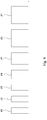
- Fig. 4 is a diagram of a Pulse Width Modulation (PWM) waveform according to some embodiments of the present disclosure.
- the control manner of the switches in the primary side circuit 110 as shown in Fig. 2 is, for example, a pulse width modulation (PWM).
- PWM pulse width modulation
- the widths of the pulse width modulation waveforms P1-P3 are normal. As shown in Fig. 4 , the widths of the pulse width modulation waveforms are increasing from the pulse width modulation waveform P4.
- the width of the pulse width modulation waveform P6 is too large, and it represents that the abnormal condition occurs, which is probably caused by the over loading condition.
- the width of the pulse width modulation waveform of the present disclosure is used as the power monitor manner.
- a width of the pulse width modulation waveform is set to be a predetermined width of the pulse width modulation waveform.
- the predetermined width of the pulse width modulation waveform is the width of the pulse width modulation waveform P5. If the processing circuit 220 determines that the width of the pulse width modulation waveform of the switch in the primary side circuit 110 is different from the predetermined width (e.g., large than the width of the pulse width modulation waveform P5), the processing circuit 220 does not output the abnormal signal to give a warning until the abnormal condition occurs (i.e., the pulse width modulation waveformP6), but outputs the abnormal signal in advance. As such, the performance decreasing/damage of the power supply device can be prevented in advance.
- the processing circuit 220 determines whether the frequency of the control signal of the switch in the primary side circuit 110 is different from the predetermined frequency. If the frequency of the pulse frequency modulation signal of the switch of the primary side circuit 110 is different from the predetermined frequency, the processing circuit 220 outputs the abnormal signal.
- the normal frequency of the pulse frequency modulation signal is ranged from 60kHz-80kHz. When the frequency of the pulse frequency modulation signal is 200kHz, it represents that the abnormal condition occurs, which is probably introduced by over loading.
- the pulse frequency modulation signal of the present disclosure is used as the power monitor manner.
- a predetermined frequency is set such as 100kHz.
- the processing circuit 220 determines that the frequency of the pulse frequency modulation signal of the switch of the primary side circuit 110 is larger than the predetermined frequency, the processing circuit 220 does not output the abnormal signal to give a warning until the abnormal condition occurs (i.e., the frequency of the pulse frequency modulation signal is 200kHz), but outputs the abnormal signal in advance. As such, the condition of performance decreasing/damage of the power supply device can be prevented in advance.
- embodiments of the present disclosure provide a power monitor.
- the power monitor of the present disclosure can forecast the condition of the power converter intelligently so as to change the element or do other related processing in advance. Therefore, the power converter can be maintained in normal condition, and almost has no chance to be damage/power failure.
- the conventional power supply device needs two power supplies. Compared with the conventional power supply device with two power supplies, the present disclosure needs single power supply. Therefore, the cost of the power supply device is reduced.
- the aging elements can be changed in advance so as to maintain the power supply in high efficiency condition, such that the output ripple wave can be prevented from becoming larger or other related standards of the power supply device can be prevented from being abnormal.
Landscapes
- Physics & Mathematics (AREA)
- General Physics & Mathematics (AREA)
- Engineering & Computer Science (AREA)
- General Engineering & Computer Science (AREA)
- Theoretical Computer Science (AREA)
- Computer Hardware Design (AREA)
- Microelectronics & Electronic Packaging (AREA)
- Dc-Dc Converters (AREA)
Abstract
Description
- The present invention relates to a monitor device. More particularly, the present invention relates to an intelligence power monitor.
- In industry application, all kinds of machines that produce products need stable and uninterruptible power, so as to prevent the power from being abnormal or to prevent the power failure of the power from being occurred, such that the loss of the factory can be reduced.
- For preventing the power from being abnormal or to prevent the power failure of the power from being occurred, a conventional power supply device has two power supplies. When any one of the power supplies is abnormal and needs to be repaired, the other one of the power supplies maintains supplying power. Another way is that the conventional power supply device has an uninterruptible power system (UPS). When the power supply device damages or the power failure of the power supply device occurs, the UPS can provide power to machines.
- However, the conventional power supply device needs to have two power supplies, and the cost is therefore higher. No matter the conventional power supply device adopts having two power supplies manner or having UPS manner to maintain supplying power, this is a remedy after the conventional power supply device is already damaged or the power failure of the conventional power supply device occurs. The loss of the factory cost by the power supply device being damaged or the power failure of the conventional power supply device occurring is extremely high. The loss of the factory is sometimes beyond compute. Therefore, how to reduce the cost of the power supply device, and how to prevent the power supply device from being damaged or to prevent the power failure of the power supply device from occurring is a problem to be improved in the field.
- The following presents a simplified summary of the disclosure in order to provide a basic understanding to the reader. This summary is not an extensive overview of the disclosure and it does not identify key/critical elements of the present invention or delineate the scope of the present invention.
- One aspect of the present disclosure is directed to a power monitor. The power monitor comprises a detecting circuit, a processing circuit, and a warning circuit. The detecting circuit detects a first abnormal condition of a primary side circuit and a second abnormal condition of a secondary side circuit. The processing circuit calculates a first class and a first occurring number of the first abnormal condition, and calculates a second class and a second occurring number of the second abnormal condition. The processing circuit determines whether the first occurring number is larger than a first predetermined number corresponding to the first class; if it is, the processing circuit outputs a first abnormal signal. The processing circuit determines whether the second occurring number is larger than a second predetermined number corresponding to the second class; if it is, the processing circuit outputs a second abnormal signal. The warning circuit outputs a warning signal according to the first abnormal signal or the second abnormal signal.
- Another aspect of the present disclosure is directed to a power monitor. The power monitor comprises a detecting circuit, a processing circuit, and a warning circuit. The detecting circuit is configured to detect an input voltage of a primary side circuit of a power converter. The processing circuit is configured to compare a condition of the input voltage and a predetermined parameter, wherein if the condition of the input voltage and the predetermined parameter are different, the processing circuit outputs an abnormal signal. The warning circuit is configured to output a warning signal according to the abnormal signal.
- These and other features, aspects, and advantages of the present invention, as well as the technical means and embodiments employed by the present invention, will become better understood with reference to the following description in connection with the accompanying drawings and appended claims.
- The invention can be more fully understood by reading the following detailed description of the embodiment, with reference made to the accompanying drawings as follows:
-
Fig. 1 is a circuit block diagram of a power supply device according to some embodiments of the present disclosure. -
Fig. 2 is a diagram of a power converter of the power supply device as illustrated inFig. 1 according to some embodiments of the present disclosure. -
Fig. 3 is a diagram of a voltage waveform according to some embodiments of the present disclosure. -
Fig. 4 is a diagram of a Pulse Width Modulation (PWM) waveform according to some embodiments of the present disclosure. - In accordance with common practice, the various described features/elements are not drawn to scale but instead are drawn to best illustrate specific features/elements relevant to the present invention. Also, wherever possible, like or the same reference numerals are used in the drawings and the description to refer to the same or like parts.
- The detailed description provided below in connection with the appended drawings is intended as a description of the present examples and is not intended to represent the only forms in which the present example may be constructed or utilized. The description sets forth the functions of the example and the sequence of steps for constructing and operating the example. However, the same or equivalent functions and sequences may be accomplished by different examples.
- Unless otherwise defined herein, scientific and technical terminologies employed in the present disclosure shall have the meanings that are commonly understood and used by one of ordinary skill in the art. Unless otherwise required by context, it will be understood that singular terms shall include plural forms of the same and plural terms shall include singular forms of the same.
-
Fig. 1 is a circuit block diagram of a power supply device according to some embodiments of the present disclosure. As shown in the figure, the power supply device includes apower converter 100 and apower monitor 200. Thepower monitor 200 includes a detectingcircuit 210, aprocessing circuit 220, awarning circuit 230 and acommunication circuit 240. With respect to connection, thepower converter 100 is connected to apower 800 and aload 900. The detectingcircuit 210 is connected to aprimary side circuit 110 of thepower converter 100, and connected to asecondary side circuit 120 of thepower converter 100. Theprocessing circuit 220 is connected to the detectingcircuit 210. Thewarning circuit 230 is connected to theprocessing circuit 220. Thecommunication circuit 240 is connected to thewarning circuit 230. - With respect to operation, the
power converter 100 transforms the energy provided by thepower 800, and provides it to theload 900. In one embodiment, thepower 800 can be but not limited to the power grid or other outer power. Thepower monitor 200 is configured to monitor the condition of thepower converter 100, and inform users immediately when thepower converter 100 is abnormal, so as to prevent the power supply device from being damage/power failure, which will be described in detail as below. - The detecting
circuit 210 of thepower monitor 200 detects a first abnormal condition of theprimary side circuit 110 of thepower converter 100 and a second abnormal condition of thesecondary side circuit 120 of thepower converter 100 in real time. Theprocessing circuit 220 then calculates a first class and a first occurring number of the first abnormal condition, and calculates a second class and a second occurring number of the second abnormal condition. For example, when the energy provided by thepower 800 is high, theprimary side circuit 110 will receive a high voltage. Meanwhile, the detectingcircuit 210 will detect the above-mentioned abnormal condition, and theprocessing circuit 220 then calculates a class of the abnormal condition (e.g., 1000 volts/750 volts are two kinds of different classes) and a happened number of the abnormal condition. In addition, when the electricity usage demand of theload 900 increases, an overload condition will happen in thesecondary side circuit 120. Meanwhile, the detectingcircuit 210 will detect the above-mentioned abnormal condition, theprocessing circuit 220 then calculates the class of the abnormal condition (e.g., overload time: 10 seconds/overload time: 3 seconds are two kinds of different classes) and the happened number of the abnormal condition. - Subsequently, the
processing circuit 220 of thepower monitor 200 further determines whether a first occurring number is larger than a first predetermined number corresponding to the first class. If it is, theprocessing circuit 220 outputs a first abnormal signal. Besides, theprocessing circuit 220 determines whether a second occurring number is larger than a second predetermined number corresponding to the second class. If it is, theprocessing circuit 220 outputs a second abnormal signal. In one embodiment, theprocessing circuit 220 receives the first predetermined number corresponding to the first class and the second predetermined number corresponding to the second class from a look-up table. For example, theprocessing circuit 220 receives a related predetermined number according to the class of the abnormal condition of the primary side circuit 110 (e.g., 1000 volts/ 750volts). When the class of the abnormal condition is 1000 volts, the damage to theprimary side circuit 110 is high due to the abnormal voltage is high. Therefore, the acceptable number of the 1000 volts is predetermined to be 5. If the shock number to theprimary side circuit 110 is more than 5, theprocessing circuit 220 outputs the abnormal signal. In contrast, when the class of the abnormal condition is 750 volts, the damage to theprimary side circuit 110 is low due to the abnormal voltage is low. Therefore, the acceptable number of the 750 volts is predetermined to be 20. If the shock number to theprimary side circuit 110 is more than 20, theprocessing circuit 220 then outputs the abnormal signal. - The condition of the
secondary side circuit 120 is that theprocessing circuit 220 receives a corresponding predetermined number according to the class of the abnormal condition of the secondary side circuit 120 (e.g., overload time: 10 seconds/overload time: 3 seconds). When the class of the abnormal condition is that the overload time is 10 seconds, the damage to thesecondary side circuit 120 is high due to the overload time is long. Therefore, the acceptable number of the 10 seconds overload time is predetermined to be 50. If the happened time of the overload condition to thesecondary side circuit 120 is more than 50, theprocessing circuit 220 outputs the abnormal signal. In contrast, when the class of the abnormal condition is that the overload time is 3 seconds, the damage to thesecondary side circuit 120 is low due to the overload time is low. Therefore, the acceptable number of the 3 seconds overload time is predetermined to be 100. If the happened time of the overload condition to thesecondary side circuit 120 is more than 100, theprocessing circuit 220 then outputs the abnormal signal. - In addition, the
warning circuit 230 will output a warning signal according to the first abnormal signal corresponding to theprimary side circuit 110, or thewarning circuit 230 will output the warning signal according to the second abnormal signal corresponding to thesecondary side circuit 120. For example, when the shock number to theprimary side circuit 110 by 1000 volts is more than 5, the damage of elements inside theprimary side circuit 110 may achieve the damage tolerance. The elements inside theprimary side circuit 110 will break down at any time if keep using the elements. Meanwhile, thewarning circuit 230 will output the warning signal, so as to remind users to change the elements inside theprimary side circuit 110, in order to avoid damage/power failure of the power supply device. Similarly, when the happened time of the 10 seconds overload condition to thesecondary side circuit 120 is more than 50, the damage of the elements inside thesecondary side circuit 120 may achieve the damage tolerance. The elements inside thesecondary side circuit 120 will break down at any time if keep using the elements. Meanwhile, thewarning circuit 230 will output the warning signal, so as to remind users to change the elements inside thesecondary side circuit 120, in order to avoid damage/power failure of the power supply device. - The abnormal conditions of the
primary side circuit 110 and thesecondary side circuit 120 of thepower converter 100 in the present disclosure are not intended to be limited to the above-mentioned embodiments. For example, the abnormal condition of theprimary side circuit 110 can also be voltage abnormal, current abnormal, surge or other condition which may damage circuits, and the abnormal condition of thesecondary side circuit 120 can also be voltage abnormal, current abnormal, overload or other condition which may damage circuits. - In one embodiment, the
power monitor 200 of the present disclosure can be used in remote monitor field. Thepower monitor 200 may include acommunication circuit 240. If theprimary side circuit 110 or thesecondary side circuit 120 of thepower converter 100 is abnormal, thecommunication circuit 240 can be used to transmit the warning signal to a remote monitor system (not shown) through a wired manner or a wireless manner, such that users can monitor the power converters easily in a remote manner. If the abnormal condition happens, staff whose location near theabnormal power converter 100 will be noticed to fix theabnormal power converter 100. In addition, thepower monitor 200 further uses the detectingcircuit 210 to detect theprimary side circuit 110 or thesecondary side circuit 120 of thepower converter 100 for generating detection data. Thecommunication circuit 240 is further used to transmit detailed detection data (e.g., abnormal condition data) to the remote monitor system. The remote monitor system collects all conditions for big data analyzing, and adaptively adjusts thepower monitor 200 or the parameter of the look-up table according to analyzing result, such that thepower monitor 200 can further monitor and give a waring intelligently. -
Fig. 2 is a detailed circuit diagram of apower converter 100 as illustrated inFig. 1 according to some embodiments of the present disclosure. Thepower converter 100 used herein is a flyback converter. However, the embodiment is used for illustration purpose, and the present disclosure is not limited to the circuit as shown in the embodiment regardingFig. 2 . Thepower converter 100 can be a forward converter, a half-bridge converter, a full-bridge converter or other type converter. - Reference is now made to both
Fig. 1 andFig. 2 . The detectingcircuit 210 of thepower monitor 200 is configured to detect the input voltage of theprimary side circuit 110. The input voltage of theprimary side circuit 110 herein refers to the DC voltage at any position after the bridge rectifier circuit of theprimary side circuit 110 inFig. 2 , such as the voltage of input capacitor C, resistor, switch(includes the PWM/PFM waveform), diode, etc. Subsequently, theprocessing circuit 220 is configured to compare a condition of the input voltage and a predetermined parameter. If the condition of the input voltage and the predetermined parameter are different, theprocessing circuit 220 outputs an abnormal signal. Thewarning circuit 230 then outputs a warning signal according to the abnormal signal. The warning signal is transmitted to a remote monitor device (not shown) through thecommunication circuit 240 so as to notice users. In addition, for facilitating the understanding of the technology of the power monitor in the present disclosure, reference is made toFig. 3 , which is a diagram of a voltage waveform according to some embodiments of the present disclosure. The voltage waveform W1 as shown inFig. 3 is the input voltage waveform of the input capacitor C of theprimary side circuit 110 as shown inFig. 2 , and the voltage waveform W2 as shown inFig. 3 is the output voltage waveform of thesecondary side circuit 120 as shown inFig. 2 . The present disclosure has multiple power monitor technologies, which will be described in detail as below. - Reference is now made to
Figs. 1-3 . With respect to wave trough detection, theprocessing circuit 220 is configured to determine whether a wave trough of the input voltage W1 is lower than a predetermined wave trough voltage. For example, a predetermined wave trough voltage L2 is set. If the wave trough of the input voltage W1 is lower than the predetermined wave trough voltage L2 (i.e., the A point as shown inFig. 3 ), it represents that an abnormal condition occurs. Meanwhile, theprocessing circuit 220 outputs the abnormal signal. Aging process of the input capacitor C occurs when the input capacitor C is used after a period of time. If the input capacitor is an electrolytic capacitor, the electrolyte solution therein will decrease as time goes on, such that the performance of the input capacitor declines. Conventional detection manner is to detect the output voltage W2 of the secondary side circuit, and a waring is given when the output voltage W2 is abnormal. However, as discussed above, the element that introduces problems is in the primary side circuit, which results in the decreasing of the input voltage W1. The conventional manner, to give a waring when detecting that the output voltage W2 of the secondary side circuit being abnormal, is putting the cart before the horse. If the wave trough detection manner of the present disclosure is used as the power monitor manner, the aging process of the input capacitor C of theprimary side circuit 110 will be found directly/efficiently (i.e., detecting that the input voltage W1 is lower than the predetermined wave trough voltage L2, which represents the input capacitor C ages), such that the input capacitor C can be changed immediately. As such, the condition of performance decreasing/damage of the power supply device can be prevented in advance so as to prevent the output ripple wave from becoming larger. - With respect to peak value detection, the
processing circuit 220 is configured to determine whether a peak of the input voltage W1 is larger than a predetermined peak voltage value. For example, a predetermined peak voltage value L1 is set. If the peak of the input voltage W1 is larger than the predetermined peak voltage value L1, it represents that an abnormal condition occurs. Meanwhile, theprocessing circuit 220 outputs the abnormal signal. For detecting whether power provided by an outer power (e.g., a power grid) is abnormal, conventional detection manner is to detect the output voltage W2 of the secondary side circuit as well, and a waring is given when the output voltage W2 is abnormal. However, as discussed above, the element that introduces problems is in the primary side circuit receiving power from the outer power, which results in the increasing of the input voltage W1. The conventional manner, to give a waring when detecting that the output voltage W2 of the secondary side circuit being abnormal, is also putting the cart before the horse. If the peak value detection manner of the present disclosure is used as the power monitor manner, the input voltage W1 of theprimary side circuit 110 can be detected in a real time. If the peak of the input voltage W1 is larger than a predetermined peak voltage value for too many times, the input capacitor C will be damaged seriously. Meanwhile, the input capacitor C can be changed immediately. As such, the condition of performance decreasing/damage of the power supply device can be prevented in advance so as to prevent the output ripple wave from becoming larger. - With respect to difference value detection, the
processing circuit 220 is configured to determine whether a wave motion difference value of the input voltage (i.e. a peak to peak value of the input voltage) is larger than a predetermined voltage difference value. If the wave motion difference value of the input voltage is larger than the predetermined voltage difference value, it represents that a wave motion of a power provided by thepower 800 is too large. As such, the input capacitor C will also be damaged. Conventional detection manner is to detect the output voltage W2 of the secondary side circuit as well, and a waring is given when the output voltage W2 is abnormal. However, as discussed above, the element that introduces problems is in the primary side circuit. The conventional manner, to give a waring when detecting that the output voltage W2 of the secondary side circuit is abnormal, is also putting the cart before the horse. The difference value detection manner of the present disclosure is used as the power monitor manner. If the wave motion difference value of the input voltage W1 is larger than a predetermined wave motion difference value for too many times, the input capacitor C of theprimary side circuit 110 will be damaged seriously. At this time, the input capacitor C can be changed immediately. As such, the condition of performance decreasing/damage of the power supply device can be prevented in advance so as to prevent the output ripple wave from becoming larger. - With respect to unit time variation rate detection, the
processing circuit 220 is configured to determine whether the unit time variation rate of the input voltage waveform is larger than predetermined unit time variation rate. If the unit time variation rate of the input voltage waveform is larger than a predetermined unit time variation rate (i.e., the point B as shown inFig. 3 ), it represents that an over load condition occurs. As such, the capacitor C will also be damaged. If the over load condition happens for too many times, the input capacitor C will be damaged seriously. Meanwhile, the input capacitor C can be changed immediately. As such, the condition of performance decreasing/damage of the power supply device can be prevented in advance so as to prevent the output ripple wave from becoming larger. In addition, when the over load condition happens, that is the output current of thesecondary side circuit 120 is too large - (i.e., the output current is larger than a predetermined output current), the
processing circuit 220 outputs the protection signal to a remote monitor system (not shown) in advance. The remote monitor system can monitor the whole system, and the remote monitor system controls thepower converter 100 in advance so as to prevent the power supply device from damage. Subsequently, theprocessing circuit 220 outputs the abnormal signal to thewarning circuit 230, and thewarning circuit 230 outputs the warning signal to notice users to do related processing. For example, theprocessing circuit 220 can output the protection signal to the remote monitor system in advance, and the remote monitor system changes thepower converter 100, lowers the load of thepower converter 100 or to do other suitable processing. As such, before thewarning circuit 230 notices users to do related processing, thepower converter 100 can be protected by performing protection processes in advance so as to further prevent the power supply device from damage. -
Fig. 4 is a diagram of a Pulse Width Modulation (PWM) waveform according to some embodiments of the present disclosure. The control manner of the switches in theprimary side circuit 110 as shown inFig. 2 is, for example, a pulse width modulation (PWM). The widths of the pulse width modulation waveforms P1-P3 are normal. As shown inFig. 4 , the widths of the pulse width modulation waveforms are increasing from the pulse width modulation waveform P4. The width of the pulse width modulation waveform P6 is too large, and it represents that the abnormal condition occurs, which is probably caused by the over loading condition. The width of the pulse width modulation waveform of the present disclosure is used as the power monitor manner. A width of the pulse width modulation waveform is set to be a predetermined width of the pulse width modulation waveform. For example, the predetermined width of the pulse width modulation waveform is the width of the pulse width modulation waveform P5. If theprocessing circuit 220 determines that the width of the pulse width modulation waveform of the switch in theprimary side circuit 110 is different from the predetermined width (e.g., large than the width of the pulse width modulation waveform P5), theprocessing circuit 220 does not output the abnormal signal to give a warning until the abnormal condition occurs (i.e., the pulse width modulation waveformP6), but outputs the abnormal signal in advance. As such, the performance decreasing/damage of the power supply device can be prevented in advance. In addition, with respect to frequency detection, when the control manner of the switch in theprimary side circuit 110 is changed into pulse frequency modulation (PFM), theprocessing circuit 220 determines whether the frequency of the control signal of the switch in theprimary side circuit 110 is different from the predetermined frequency. If the frequency of the pulse frequency modulation signal of the switch of theprimary side circuit 110 is different from the predetermined frequency, theprocessing circuit 220 outputs the abnormal signal. For example, the normal frequency of the pulse frequency modulation signal is ranged from 60kHz-80kHz. When the frequency of the pulse frequency modulation signal is 200kHz, it represents that the abnormal condition occurs, which is probably introduced by over loading. The pulse frequency modulation signal of the present disclosure is used as the power monitor manner. A predetermined frequency is set such as 100kHz. If theprocessing circuit 220 determines that the frequency of the pulse frequency modulation signal of the switch of theprimary side circuit 110 is larger than the predetermined frequency, theprocessing circuit 220 does not output the abnormal signal to give a warning until the abnormal condition occurs (i.e., the frequency of the pulse frequency modulation signal is 200kHz), but outputs the abnormal signal in advance. As such, the condition of performance decreasing/damage of the power supply device can be prevented in advance. - In view of the above embodiments of the present disclosure, it is apparent that the application of the present invention has the advantages as follows. In view of the foregoing, embodiments of the present disclosure provide a power monitor. The power monitor of the present disclosure can forecast the condition of the power converter intelligently so as to change the element or do other related processing in advance. Therefore, the power converter can be maintained in normal condition, and almost has no chance to be damage/power failure. For preventing the conventional power supply device from damage/power failure, the conventional power supply device needs two power supplies. Compared with the conventional power supply device with two power supplies, the present disclosure needs single power supply. Therefore, the cost of the power supply device is reduced. In addition, the aging elements can be changed in advance so as to maintain the power supply in high efficiency condition, such that the output ripple wave can be prevented from becoming larger or other related standards of the power supply device can be prevented from being abnormal.
Claims (15)
- A power monitor (200), characterized by comprising:a detecting circuit (210) configured to detect a first abnormal condition of a primary side circuit (110) of a power converter (100) and a second abnormal condition of a secondary side circuit (120) of the power converter (100);a processing circuit (220) configured to calculate a first class and a first occurring number of the first abnormal condition, and calculate a second class and a second occurring number of the second abnormal condition, wherein the processing circuit (220) determines whether the first occurring number is larger than a first predetermined number corresponding to the first class; if it is, the processing circuit (220) outputs a first abnormal signal, wherein the processing circuit (220) determines whether the second occurring number is larger than a second predetermined number corresponding to the second class; if it is, the processing circuit (220) outputs a second abnormal signal; anda warning circuit (230) configured to output a warning signal according to the first abnormal signal or the second abnormal signal.
- The power monitor (200) of claim 1, wherein the processing circuit (220) obtains the first predetermined number corresponding to the first class from a look-up table, and obtains the second predetermined number corresponding to the second class from the look-up table.
- The power monitor (200) of claim 2, wherein the warning circuit (230) comprises a communication circuit (240), and the communication circuit (240) is configured to transmit the warning signal to a remote monitor system.
- The power monitor (200) of claim 3, wherein the detecting circuit (210) is further configured to detect the primary side circuit (110) and the secondary side circuit (120) of the power converter (100) so as to generate a detected data, wherein the communication circuit (240) transmits the detected data to the remote monitor system such that the remote monitor system analyzes the detected data, and adjusts parameters of the look-up table according to an analyzed result of the detected data.
- The power monitor (200) of any one of claims 1 to 4, wherein the power converter (100) comprise one of a forward converter, a flyback converter, a half-bridge converter, and a full-bridge converter.
- The power monitor (200) of any one of claims 1 to 5, wherein the first abnormal condition of the primary side circuit (110) comprises one of a voltage abnormal, a current abnormal, and a surge.
- The power monitor (200) of any one of claims 1 to 6, wherein the second abnormal condition of the secondary side circuit (120) comprises one of a voltage abnormal, a current abnormal, and an overload.
- A power monitor (200), characterized by comprising:a detecting circuit (210) configured to detect an input voltage (W1, P1-P7) of a primary side circuit (110) of a power converter (100);a processing circuit (220) configured to compare a condition of the input voltage (W1, P1-P7) and a predetermined parameter, wherein if the condition of the input voltage (W1, P1-P7) and the predetermined parameter are different, the processing circuit outputs an abnormal signal; anda warning circuit (230) configured to output a warning signal according to the abnormal signal.
- The power monitor (200) of claim 8, wherein the processing circuit (220) is configured to determine whether a wave trough of the input voltage (W1) is lower than a predetermined voltage, wherein if the wave trough of the input voltage (W1) is lower than the predetermined voltage, the processing circuit (220) outputs the abnormal signal.
- The power monitor (200) of claim 8 or 9, wherein the processing circuit (220) configured to determine whether a peak of the input voltage (W1) is larger than a predetermined voltage, wherein if the peak of the input voltage (W1) is larger than the predetermined voltage, the processing circuit (220) outputs the abnormal signal.
- The power monitor (200) of any one of claims 8 to 10, wherein the processing circuit (220) configured to determine whether a wave motion difference value of the input voltage (W1) is larger than a predetermined voltage difference value, wherein if the wave motion difference value of the input voltage (W1) is larger than the predetermined voltage difference value, the processing circuit (220) outputs the abnormal signal.
- The power monitor (200) of any one of claims 8 to 11, wherein the processing circuit (220) configured to determine whether a waveform unit time variation rate of the input voltage (W1) is larger than a predetermined unit time variation rate, wherein if the waveform unit time variation rate of the input voltage (W1) is larger than the predetermined unit time variation rate, the processing circuit (220) outputs the abnormal signal.
- The power monitor (200) of any one of claims 8 to 12, wherein the processing circuit (220) configured to determine whether a width of a pulse width modulation waveform (P1-P7) of a switch in the primary side circuit (110) is different from a predetermined width, wherein if the width of the pulse width modulation waveform (P1-P7) of the switch in the primary side circuit (110) is different from the predetermined width, the processing circuit (220) outputs the abnormal signal.
- The power monitor (200) of any one of claims 8 to 13, wherein the processing circuit (220) configured to determine whether a frequency of a switch of the primary side circuit (110) is different from a predetermined frequency, wherein if the frequency of the switch of the primary side circuit (110) is different from the predetermined frequency, the processing circuit (220) outputs the abnormal signal.
- The power monitor (200) of any one of claims 8 to 14, wherein the detecting circuit (210) further configured to detect an output current of a secondary side circuit (120) of the power converter (100), wherein in condition that the processing circuit (220) compares and determines that the output current of the secondary side circuit (120) of the power converter (100) is larger than a predetermined output current, the processing circuit (220) outputs the abnormal signal after the processing circuit (220) outputs a protection signal to a remote monitor system.
Applications Claiming Priority (1)
| Application Number | Priority Date | Filing Date | Title |
|---|---|---|---|
| CN201810588440.1A CN110579720B (en) | 2018-06-08 | 2018-06-08 | Power supply monitor |
Publications (3)
| Publication Number | Publication Date |
|---|---|
| EP3579000A1 true EP3579000A1 (en) | 2019-12-11 |
| EP3579000B1 EP3579000B1 (en) | 2024-04-10 |
| EP3579000C0 EP3579000C0 (en) | 2024-04-10 |
Family
ID=66770317
Family Applications (1)
| Application Number | Title | Priority Date | Filing Date |
|---|---|---|---|
| EP19178379.4A Active EP3579000B1 (en) | 2018-06-08 | 2019-06-05 | Power supply with power monitor |
Country Status (3)
| Country | Link |
|---|---|
| US (2) | US11507168B2 (en) |
| EP (1) | EP3579000B1 (en) |
| CN (1) | CN110579720B (en) |
Families Citing this family (5)
| Publication number | Priority date | Publication date | Assignee | Title |
|---|---|---|---|---|
| CN111532925B (en) * | 2020-03-27 | 2021-10-22 | 日立电梯(中国)有限公司 | Elevator power protection method |
| CN114545282A (en) * | 2020-11-24 | 2022-05-27 | 青岛海尔电冰箱有限公司 | Power failure detection method and device and power utilization equipment with same |
| CN114545283B (en) * | 2020-11-24 | 2025-10-31 | 青岛海尔电冰箱有限公司 | Power failure detection device and electric equipment |
| CN114217240B (en) * | 2021-12-06 | 2024-01-23 | 上海德衡数据科技有限公司 | Uninterruptible power supply detection method and system |
| CN120405494A (en) * | 2025-05-22 | 2025-08-01 | 苏州美恩斯电子科技有限公司 | A high-power power supply output deviation detection system and method |
Citations (5)
| Publication number | Priority date | Publication date | Assignee | Title |
|---|---|---|---|---|
| US20050189348A1 (en) * | 2001-06-04 | 2005-09-01 | Matsushita Electric Industrial Co., Ltd. | Magnetron drive power supply |
| US20060186892A1 (en) * | 2003-07-30 | 2006-08-24 | Kabushiki Kaisha Yaskawa Denki | Open-phase detecting method and apparatus |
| WO2015059906A1 (en) * | 2013-10-21 | 2015-04-30 | パナソニックIpマネジメント株式会社 | Power supply control apparatus |
| US9429601B2 (en) * | 2012-03-26 | 2016-08-30 | Sanken Electric Co., Ltd. | Alternating current input voltage detection circuit |
| DE102016008053A1 (en) | 2016-07-01 | 2017-02-16 | Daimler Ag | Precharging a DC link capacitance of a DC intermediate circuit |
Family Cites Families (29)
| Publication number | Priority date | Publication date | Assignee | Title |
|---|---|---|---|---|
| EP1257048B1 (en) * | 2001-05-09 | 2017-10-04 | Philips Lighting Holding B.V. | Regulation device for a resonant converter |
| CN100553086C (en) * | 2004-03-15 | 2009-10-21 | 株式会社日立医药 | Power conversion device, inverter X-ray high voltage device, X-ray fluoroscopy camera device, X-ray CT device, MRI device |
| CN100489931C (en) * | 2004-09-06 | 2009-05-20 | 索尼株式会社 | Image display unit and method of driving the same |
| JP4759968B2 (en) * | 2004-10-04 | 2011-08-31 | ダイキン工業株式会社 | Method and apparatus for protecting PWM rectifier circuit |
| JP2008271696A (en) * | 2007-04-19 | 2008-11-06 | Toshiba Elevator Co Ltd | Power conversion apparatus |
| CN201072438Y (en) * | 2007-05-15 | 2008-06-11 | 北京索英电气技术有限公司 | Multi-input channel modular high-frequency isolated single-phase power feedback electronic load |
| JP4621231B2 (en) * | 2007-06-29 | 2011-01-26 | 富士通テン株式会社 | Power supply protection device and electronic control device |
| CN101572501B (en) * | 2008-04-30 | 2011-08-03 | 深超光电(深圳)有限公司 | Monitoring circuit |
| CN101435839B (en) * | 2008-12-09 | 2011-09-14 | 中国西电电气股份有限公司 | Method for monitoring light trigger pulse of power electronic device |
| US8674667B2 (en) * | 2009-12-29 | 2014-03-18 | Fsp Technology Inc. | Post regulation control circuit |
| CN102130574B (en) * | 2010-01-13 | 2013-06-19 | 台达电子工业股份有限公司 | Multi-output step-down conversion device with controllable energy release function |
| EP2542906B1 (en) * | 2010-03-02 | 2015-05-06 | Accumetrics, Inc. | Method and apparatus for fault detection of series diodes in rectifiers |
| JP5104892B2 (en) * | 2010-03-09 | 2012-12-19 | オムロン株式会社 | Switching power supply |
| JP5642031B2 (en) * | 2011-08-01 | 2014-12-17 | Jx日鉱日石エネルギー株式会社 | Ground fault detection device, ground fault detection method, solar power generation system, and ground fault detection program |
| KR101327591B1 (en) * | 2012-07-02 | 2013-11-12 | 엘에스산전 주식회사 | Apparatus for diagnosing dc link capacitor of inverter |
| CN103675634A (en) * | 2012-09-14 | 2014-03-26 | 上海英恒电子有限公司 | Method for testing IGBT (Insulated Gate Bipolar Transistor) based on LabVIEW |
| US9793753B2 (en) * | 2012-09-21 | 2017-10-17 | Schneider Electric It Corporation | Power quality detector |
| CN104782021B (en) * | 2012-11-15 | 2017-05-24 | Abb技术有限公司 | Circuit structure and method for reducing power consumption of equipment including active module and standby module |
| CN103257297B (en) * | 2013-05-10 | 2015-06-10 | 电子科技大学 | System and method for testing dynamic energy exchange performance of electricity energy-storing device |
| CN104422806B (en) * | 2013-08-21 | 2018-08-07 | 鸿富锦精密工业(深圳)有限公司 | power detection circuit |
| EP2869430B1 (en) * | 2013-10-29 | 2020-03-11 | Velvetwire LLC | Software controlled power supply and battery charger |
| US10324512B2 (en) * | 2013-10-30 | 2019-06-18 | Lenovo (Singapore) Pte. Ltd. | Device power management based on detected power source |
| CN104698377A (en) * | 2013-12-04 | 2015-06-10 | 大连东浦机电有限公司 | Motor operation monitoring method |
| DE102014105909A1 (en) | 2014-04-28 | 2015-10-29 | Phoenix Contact Gmbh & Co. Kg | Power supply unit |
| US9748759B1 (en) * | 2014-05-09 | 2017-08-29 | Donald J. Bergeron | Lightning electromagnetic pulse (LEMP) detector and isolation device |
| CN104122479B (en) * | 2014-07-29 | 2017-04-19 | 华中科技大学 | Online detection method for open-circuit faults of power tubes of induction-motor vector control system |
| CN105891658B (en) * | 2016-06-06 | 2019-04-12 | 安徽大学 | A kind of diagnostic method of open-circuit fault of power tubes of inverter |
| US10186855B2 (en) * | 2016-10-04 | 2019-01-22 | Abb Schweiz Ag | Differential fault detection system |
| CN107045099A (en) * | 2017-04-26 | 2017-08-15 | 哈尔滨理工大学 | A kind of bipolarity multiple-pulse turn-to-turn insulation test system and method for testing |
-
2018
- 2018-06-08 CN CN201810588440.1A patent/CN110579720B/en active Active
-
2019
- 2019-01-24 US US16/257,020 patent/US11507168B2/en active Active
- 2019-06-05 EP EP19178379.4A patent/EP3579000B1/en active Active
-
2022
- 2022-09-08 US US17/930,419 patent/US11630501B2/en active Active
Patent Citations (5)
| Publication number | Priority date | Publication date | Assignee | Title |
|---|---|---|---|---|
| US20050189348A1 (en) * | 2001-06-04 | 2005-09-01 | Matsushita Electric Industrial Co., Ltd. | Magnetron drive power supply |
| US20060186892A1 (en) * | 2003-07-30 | 2006-08-24 | Kabushiki Kaisha Yaskawa Denki | Open-phase detecting method and apparatus |
| US9429601B2 (en) * | 2012-03-26 | 2016-08-30 | Sanken Electric Co., Ltd. | Alternating current input voltage detection circuit |
| WO2015059906A1 (en) * | 2013-10-21 | 2015-04-30 | パナソニックIpマネジメント株式会社 | Power supply control apparatus |
| DE102016008053A1 (en) | 2016-07-01 | 2017-02-16 | Daimler Ag | Precharging a DC link capacitance of a DC intermediate circuit |
Also Published As
| Publication number | Publication date |
|---|---|
| US20230004203A1 (en) | 2023-01-05 |
| CN110579720B (en) | 2022-08-30 |
| CN110579720A (en) | 2019-12-17 |
| EP3579000B1 (en) | 2024-04-10 |
| US11507168B2 (en) | 2022-11-22 |
| US11630501B2 (en) | 2023-04-18 |
| EP3579000C0 (en) | 2024-04-10 |
| US20190377398A1 (en) | 2019-12-12 |
Similar Documents
| Publication | Publication Date | Title |
|---|---|---|
| US11630501B2 (en) | Power monitor | |
| US8699243B2 (en) | Power converter system with synchronous rectifier output stage and reduced no-load power consumption | |
| US8084886B2 (en) | Uninterruptible power supply apparatus | |
| EP3076537A1 (en) | Power source apparatus and electric device | |
| WO2018113704A1 (en) | A switching arrangement for switching between two inputs, equipment, system and a method | |
| US10110058B2 (en) | Power conversion device and method for preventing abnormal shutdown thereof | |
| EP1494342A2 (en) | An under-Voltage detection circuit | |
| TW201902067A (en) | Power supply | |
| EP3168961B1 (en) | Uninterruptible power source device | |
| CN112290800A (en) | X capacitor discharge control circuit and method and switching power supply | |
| EP2518885B1 (en) | Power converter having semiconductor switching element | |
| KR102112077B1 (en) | Uninterruptible power supply with single winding of output winding and inverter winding | |
| JP5008465B2 (en) | Uninterruptible power system | |
| KR102029964B1 (en) | Apparatus for charging battery using induction current of gis enclosure | |
| US9099931B2 (en) | Power supply device | |
| TW202001267A (en) | Power monitor | |
| KR101183894B1 (en) | Switching mode power supply | |
| KR101610869B1 (en) | Power supply apparatus, driving method thereof, and security system incluing the same | |
| WO2017068519A1 (en) | Method of supplying an emergency supply module and emergency supply module with reduced power consumption | |
| US9948189B2 (en) | Power conversion device and method for correcting decision threshold level thereof | |
| CN117096834B (en) | Switching power supply and protection method thereof | |
| JP2008054468A (en) | Instantaneous voltage drop compensator | |
| CN213213326U (en) | X capacitor discharge control circuit and switching power supply | |
| JP2001057779A (en) | Switching power supply device | |
| KR20250056540A (en) | Automatic output compensation power supply |
Legal Events
| Date | Code | Title | Description |
|---|---|---|---|
| PUAI | Public reference made under article 153(3) epc to a published international application that has entered the european phase |
Free format text: ORIGINAL CODE: 0009012 |
|
| STAA | Information on the status of an ep patent application or granted ep patent |
Free format text: STATUS: THE APPLICATION HAS BEEN PUBLISHED |
|
| AK | Designated contracting states |
Kind code of ref document: A1 Designated state(s): AL AT BE BG CH CY CZ DE DK EE ES FI FR GB GR HR HU IE IS IT LI LT LU LV MC MK MT NL NO PL PT RO RS SE SI SK SM TR |
|
| AX | Request for extension of the european patent |
Extension state: BA ME |
|
| STAA | Information on the status of an ep patent application or granted ep patent |
Free format text: STATUS: REQUEST FOR EXAMINATION WAS MADE |
|
| 17P | Request for examination filed |
Effective date: 20200610 |
|
| RBV | Designated contracting states (corrected) |
Designated state(s): AL AT BE BG CH CY CZ DE DK EE ES FI FR GB GR HR HU IE IS IT LI LT LU LV MC MK MT NL NO PL PT RO RS SE SI SK SM TR |
|
| TPAC | Observations filed by third parties |
Free format text: ORIGINAL CODE: EPIDOSNTIPA |
|
| STAA | Information on the status of an ep patent application or granted ep patent |
Free format text: STATUS: EXAMINATION IS IN PROGRESS |
|
| 17Q | First examination report despatched |
Effective date: 20210324 |
|
| REG | Reference to a national code |
Free format text: PREVIOUS MAIN CLASS: G01R0017000000 Ref country code: DE Ref legal event code: R079 Ref document number: 602019049862 Country of ref document: DE Ipc: G01R0019000000 |
|
| GRAP | Despatch of communication of intention to grant a patent |
Free format text: ORIGINAL CODE: EPIDOSNIGR1 |
|
| RIC1 | Information provided on ipc code assigned before grant |
Ipc: G01R 31/40 20140101ALI20230929BHEP Ipc: G01R 19/00 20060101AFI20230929BHEP |
|
| STAA | Information on the status of an ep patent application or granted ep patent |
Free format text: STATUS: GRANT OF PATENT IS INTENDED |
|
| INTG | Intention to grant announced |
Effective date: 20231109 |
|
| RIN1 | Information on inventor provided before grant (corrected) |
Inventor name: CHANG, CHIEN-CHUNG Inventor name: WANG, KUAN-SHENG |
|
| GRAS | Grant fee paid |
Free format text: ORIGINAL CODE: EPIDOSNIGR3 |
|
| GRAA | (expected) grant |
Free format text: ORIGINAL CODE: 0009210 |
|
| STAA | Information on the status of an ep patent application or granted ep patent |
Free format text: STATUS: THE PATENT HAS BEEN GRANTED |
|
| AK | Designated contracting states |
Kind code of ref document: B1 Designated state(s): AL AT BE BG CH CY CZ DE DK EE ES FI FR GB GR HR HU IE IS IT LI LT LU LV MC MK MT NL NO PL PT RO RS SE SI SK SM TR |
|
| REG | Reference to a national code |
Ref country code: GB Ref legal event code: FG4D |
|
| REG | Reference to a national code |
Ref country code: CH Ref legal event code: EP |
|
| REG | Reference to a national code |
Ref country code: DE Ref legal event code: R096 Ref document number: 602019049862 Country of ref document: DE |
|
| REG | Reference to a national code |
Ref country code: IE Ref legal event code: FG4D |
|
| U01 | Request for unitary effect filed |
Effective date: 20240430 |
|
| U07 | Unitary effect registered |
Designated state(s): AT BE BG DE DK EE FI FR IT LT LU LV MT NL PT SE SI Effective date: 20240507 |
|
| U20 | Renewal fee for the european patent with unitary effect paid |
Year of fee payment: 6 Effective date: 20240522 |
|
| PG25 | Lapsed in a contracting state [announced via postgrant information from national office to epo] |
Ref country code: IS Free format text: LAPSE BECAUSE OF FAILURE TO SUBMIT A TRANSLATION OF THE DESCRIPTION OR TO PAY THE FEE WITHIN THE PRESCRIBED TIME-LIMIT Effective date: 20240810 |
|
| PG25 | Lapsed in a contracting state [announced via postgrant information from national office to epo] |
Ref country code: HR Free format text: LAPSE BECAUSE OF FAILURE TO SUBMIT A TRANSLATION OF THE DESCRIPTION OR TO PAY THE FEE WITHIN THE PRESCRIBED TIME-LIMIT Effective date: 20240410 |
|
| PG25 | Lapsed in a contracting state [announced via postgrant information from national office to epo] |
Ref country code: GR Free format text: LAPSE BECAUSE OF FAILURE TO SUBMIT A TRANSLATION OF THE DESCRIPTION OR TO PAY THE FEE WITHIN THE PRESCRIBED TIME-LIMIT Effective date: 20240711 |
|
| PG25 | Lapsed in a contracting state [announced via postgrant information from national office to epo] |
Ref country code: ES Free format text: LAPSE BECAUSE OF FAILURE TO SUBMIT A TRANSLATION OF THE DESCRIPTION OR TO PAY THE FEE WITHIN THE PRESCRIBED TIME-LIMIT Effective date: 20240410 |
|
| PG25 | Lapsed in a contracting state [announced via postgrant information from national office to epo] |
Ref country code: PL Free format text: LAPSE BECAUSE OF FAILURE TO SUBMIT A TRANSLATION OF THE DESCRIPTION OR TO PAY THE FEE WITHIN THE PRESCRIBED TIME-LIMIT Effective date: 20240410 |
|
| PG25 | Lapsed in a contracting state [announced via postgrant information from national office to epo] |
Ref country code: PL Free format text: LAPSE BECAUSE OF FAILURE TO SUBMIT A TRANSLATION OF THE DESCRIPTION OR TO PAY THE FEE WITHIN THE PRESCRIBED TIME-LIMIT Effective date: 20240410 Ref country code: NO Free format text: LAPSE BECAUSE OF FAILURE TO SUBMIT A TRANSLATION OF THE DESCRIPTION OR TO PAY THE FEE WITHIN THE PRESCRIBED TIME-LIMIT Effective date: 20240710 Ref country code: IS Free format text: LAPSE BECAUSE OF FAILURE TO SUBMIT A TRANSLATION OF THE DESCRIPTION OR TO PAY THE FEE WITHIN THE PRESCRIBED TIME-LIMIT Effective date: 20240810 Ref country code: HR Free format text: LAPSE BECAUSE OF FAILURE TO SUBMIT A TRANSLATION OF THE DESCRIPTION OR TO PAY THE FEE WITHIN THE PRESCRIBED TIME-LIMIT Effective date: 20240410 Ref country code: GR Free format text: LAPSE BECAUSE OF FAILURE TO SUBMIT A TRANSLATION OF THE DESCRIPTION OR TO PAY THE FEE WITHIN THE PRESCRIBED TIME-LIMIT Effective date: 20240711 Ref country code: ES Free format text: LAPSE BECAUSE OF FAILURE TO SUBMIT A TRANSLATION OF THE DESCRIPTION OR TO PAY THE FEE WITHIN THE PRESCRIBED TIME-LIMIT Effective date: 20240410 Ref country code: RS Free format text: LAPSE BECAUSE OF FAILURE TO SUBMIT A TRANSLATION OF THE DESCRIPTION OR TO PAY THE FEE WITHIN THE PRESCRIBED TIME-LIMIT Effective date: 20240710 |
|
| REG | Reference to a national code |
Ref country code: DE Ref legal event code: R097 Ref document number: 602019049862 Country of ref document: DE |
|
| PG25 | Lapsed in a contracting state [announced via postgrant information from national office to epo] |
Ref country code: CZ Free format text: LAPSE BECAUSE OF FAILURE TO SUBMIT A TRANSLATION OF THE DESCRIPTION OR TO PAY THE FEE WITHIN THE PRESCRIBED TIME-LIMIT Effective date: 20240410 |
|
| PG25 | Lapsed in a contracting state [announced via postgrant information from national office to epo] |
Ref country code: SK Free format text: LAPSE BECAUSE OF FAILURE TO SUBMIT A TRANSLATION OF THE DESCRIPTION OR TO PAY THE FEE WITHIN THE PRESCRIBED TIME-LIMIT Effective date: 20240410 Ref country code: RO Free format text: LAPSE BECAUSE OF FAILURE TO SUBMIT A TRANSLATION OF THE DESCRIPTION OR TO PAY THE FEE WITHIN THE PRESCRIBED TIME-LIMIT Effective date: 20240410 |
|
| PG25 | Lapsed in a contracting state [announced via postgrant information from national office to epo] |
Ref country code: SM Free format text: LAPSE BECAUSE OF FAILURE TO SUBMIT A TRANSLATION OF THE DESCRIPTION OR TO PAY THE FEE WITHIN THE PRESCRIBED TIME-LIMIT Effective date: 20240410 |
|
| PG25 | Lapsed in a contracting state [announced via postgrant information from national office to epo] |
Ref country code: SM Free format text: LAPSE BECAUSE OF FAILURE TO SUBMIT A TRANSLATION OF THE DESCRIPTION OR TO PAY THE FEE WITHIN THE PRESCRIBED TIME-LIMIT Effective date: 20240410 Ref country code: SK Free format text: LAPSE BECAUSE OF FAILURE TO SUBMIT A TRANSLATION OF THE DESCRIPTION OR TO PAY THE FEE WITHIN THE PRESCRIBED TIME-LIMIT Effective date: 20240410 Ref country code: RO Free format text: LAPSE BECAUSE OF FAILURE TO SUBMIT A TRANSLATION OF THE DESCRIPTION OR TO PAY THE FEE WITHIN THE PRESCRIBED TIME-LIMIT Effective date: 20240410 Ref country code: CZ Free format text: LAPSE BECAUSE OF FAILURE TO SUBMIT A TRANSLATION OF THE DESCRIPTION OR TO PAY THE FEE WITHIN THE PRESCRIBED TIME-LIMIT Effective date: 20240410 Ref country code: MC Free format text: LAPSE BECAUSE OF FAILURE TO SUBMIT A TRANSLATION OF THE DESCRIPTION OR TO PAY THE FEE WITHIN THE PRESCRIBED TIME-LIMIT Effective date: 20240410 |
|
| REG | Reference to a national code |
Ref country code: CH Ref legal event code: PL |
|
| PLBE | No opposition filed within time limit |
Free format text: ORIGINAL CODE: 0009261 |
|
| STAA | Information on the status of an ep patent application or granted ep patent |
Free format text: STATUS: NO OPPOSITION FILED WITHIN TIME LIMIT |
|
| 26N | No opposition filed |
Effective date: 20250113 |
|
| GBPC | Gb: european patent ceased through non-payment of renewal fee |
Effective date: 20240710 |
|
| PG25 | Lapsed in a contracting state [announced via postgrant information from national office to epo] |
Ref country code: IE Free format text: LAPSE BECAUSE OF NON-PAYMENT OF DUE FEES Effective date: 20240605 |
|
| PG25 | Lapsed in a contracting state [announced via postgrant information from national office to epo] |
Ref country code: CH Free format text: LAPSE BECAUSE OF NON-PAYMENT OF DUE FEES Effective date: 20240630 |
|
| PG25 | Lapsed in a contracting state [announced via postgrant information from national office to epo] |
Ref country code: GB Free format text: LAPSE BECAUSE OF NON-PAYMENT OF DUE FEES Effective date: 20240710 |
|
| U20 | Renewal fee for the european patent with unitary effect paid |
Year of fee payment: 7 Effective date: 20250509 |
|
| PGFP | Annual fee paid to national office [announced via postgrant information from national office to epo] |
Ref country code: TR Payment date: 20250530 Year of fee payment: 7 |
|
| PG25 | Lapsed in a contracting state [announced via postgrant information from national office to epo] |
Ref country code: CY Free format text: LAPSE BECAUSE OF FAILURE TO SUBMIT A TRANSLATION OF THE DESCRIPTION OR TO PAY THE FEE WITHIN THE PRESCRIBED TIME-LIMIT; INVALID AB INITIO Effective date: 20190605 |
|
| PG25 | Lapsed in a contracting state [announced via postgrant information from national office to epo] |
Ref country code: HU Free format text: LAPSE BECAUSE OF FAILURE TO SUBMIT A TRANSLATION OF THE DESCRIPTION OR TO PAY THE FEE WITHIN THE PRESCRIBED TIME-LIMIT; INVALID AB INITIO Effective date: 20190605 |