EP3577439B1 - Photonische schaltung zur messung einer probe - Google Patents
Photonische schaltung zur messung einer probe Download PDFInfo
- Publication number
- EP3577439B1 EP3577439B1 EP18703644.7A EP18703644A EP3577439B1 EP 3577439 B1 EP3577439 B1 EP 3577439B1 EP 18703644 A EP18703644 A EP 18703644A EP 3577439 B1 EP3577439 B1 EP 3577439B1
- Authority
- EP
- European Patent Office
- Prior art keywords
- wavelength
- range sensor
- photonic
- sample property
- sensors
- Prior art date
- Legal status (The legal status is an assumption and is not a legal conclusion. Google has not performed a legal analysis and makes no representation as to the accuracy of the status listed.)
- Active
Links
Images


Classifications
-
- G—PHYSICS
- G01—MEASURING; TESTING
- G01N—INVESTIGATING OR ANALYSING MATERIALS BY DETERMINING THEIR CHEMICAL OR PHYSICAL PROPERTIES
- G01N21/00—Investigating or analysing materials by the use of optical means, i.e. using sub-millimetre waves, infrared, visible or ultraviolet light
- G01N21/17—Systems in which incident light is modified in accordance with the properties of the material investigated
- G01N21/41—Refractivity; Phase-affecting properties, e.g. optical path length
- G01N21/45—Refractivity; Phase-affecting properties, e.g. optical path length using interferometric methods; using Schlieren methods
-
- G—PHYSICS
- G01—MEASURING; TESTING
- G01N—INVESTIGATING OR ANALYSING MATERIALS BY DETERMINING THEIR CHEMICAL OR PHYSICAL PROPERTIES
- G01N21/00—Investigating or analysing materials by the use of optical means, i.e. using sub-millimetre waves, infrared, visible or ultraviolet light
- G01N21/75—Systems in which material is subjected to a chemical reaction, the progress or the result of the reaction being investigated
- G01N21/77—Systems in which material is subjected to a chemical reaction, the progress or the result of the reaction being investigated by observing the effect on a chemical indicator
- G01N21/7703—Systems in which material is subjected to a chemical reaction, the progress or the result of the reaction being investigated by observing the effect on a chemical indicator using reagent-clad optical fibres or optical waveguides
-
- G—PHYSICS
- G01—MEASURING; TESTING
- G01N—INVESTIGATING OR ANALYSING MATERIALS BY DETERMINING THEIR CHEMICAL OR PHYSICAL PROPERTIES
- G01N21/00—Investigating or analysing materials by the use of optical means, i.e. using sub-millimetre waves, infrared, visible or ultraviolet light
- G01N21/75—Systems in which material is subjected to a chemical reaction, the progress or the result of the reaction being investigated
- G01N21/77—Systems in which material is subjected to a chemical reaction, the progress or the result of the reaction being investigated by observing the effect on a chemical indicator
- G01N21/7703—Systems in which material is subjected to a chemical reaction, the progress or the result of the reaction being investigated by observing the effect on a chemical indicator using reagent-clad optical fibres or optical waveguides
- G01N21/7746—Systems in which material is subjected to a chemical reaction, the progress or the result of the reaction being investigated by observing the effect on a chemical indicator using reagent-clad optical fibres or optical waveguides the waveguide coupled to a cavity resonator
-
- G—PHYSICS
- G01—MEASURING; TESTING
- G01N—INVESTIGATING OR ANALYSING MATERIALS BY DETERMINING THEIR CHEMICAL OR PHYSICAL PROPERTIES
- G01N21/00—Investigating or analysing materials by the use of optical means, i.e. using sub-millimetre waves, infrared, visible or ultraviolet light
- G01N21/17—Systems in which incident light is modified in accordance with the properties of the material investigated
- G01N21/41—Refractivity; Phase-affecting properties, e.g. optical path length
- G01N21/45—Refractivity; Phase-affecting properties, e.g. optical path length using interferometric methods; using Schlieren methods
- G01N2021/458—Refractivity; Phase-affecting properties, e.g. optical path length using interferometric methods; using Schlieren methods using interferential sensor, e.g. sensor fibre, possibly on optical waveguide
-
- G—PHYSICS
- G01—MEASURING; TESTING
- G01N—INVESTIGATING OR ANALYSING MATERIALS BY DETERMINING THEIR CHEMICAL OR PHYSICAL PROPERTIES
- G01N21/00—Investigating or analysing materials by the use of optical means, i.e. using sub-millimetre waves, infrared, visible or ultraviolet light
- G01N21/75—Systems in which material is subjected to a chemical reaction, the progress or the result of the reaction being investigated
- G01N21/77—Systems in which material is subjected to a chemical reaction, the progress or the result of the reaction being investigated by observing the effect on a chemical indicator
- G01N2021/7769—Measurement method of reaction-produced change in sensor
- G01N2021/7776—Index
-
- G—PHYSICS
- G01—MEASURING; TESTING
- G01N—INVESTIGATING OR ANALYSING MATERIALS BY DETERMINING THEIR CHEMICAL OR PHYSICAL PROPERTIES
- G01N21/00—Investigating or analysing materials by the use of optical means, i.e. using sub-millimetre waves, infrared, visible or ultraviolet light
- G01N21/75—Systems in which material is subjected to a chemical reaction, the progress or the result of the reaction being investigated
- G01N21/77—Systems in which material is subjected to a chemical reaction, the progress or the result of the reaction being investigated by observing the effect on a chemical indicator
- G01N2021/7769—Measurement method of reaction-produced change in sensor
- G01N2021/7779—Measurement method of reaction-produced change in sensor interferometric
Definitions
- the present disclosure relates to refractive index sensing by means of sensors such as ring resonators and other interferometric devices in a photonic circuit.
- MZIs Mach-Zehnder Interferometers
- MZI Mach-Zehnder Interferometer
- MZI devices have a relatively large footprint on the chip mainly determined by the long path length required to obtain a high sensitivity.
- each MZI sensor must be optically connected to a read-out unit individually.
- Ring resonators on the other hand have a smaller footprint, and multiple sensors can be multiplexed onto a single optical interface. In applications where many sensors are required, resonators are the preferred sensors in order to limit the number of expensive optical connections to the chip.
- the ring resonator read-out unit must acquire the spectral response of the ring resonator, which is a relatively slow measurement.
- Document EP2 267 432 A1 teaches a method according to the preamble of claim 1 and a system according to the preamble of claim 14.
- the current invention concerns a method according to claim 1, a non-transitory computer readable medium containing software instructions according to claim 13, and a system according to claim 14.
- Measurement of photonic circuits typically comprises application of input light into the photonic circuit and measuring output light out of the photonic circuit.
- the photonic circuit comprises at least two photonic sensors.
- the photonic sensors are configured to modulate output light with respect to the input light, i.e. they act as a wavelength filter, where the sensor is configured such that the filter function depends on a specific measured quantity.
- Signal values of the output signals periodically recur as a function of a wavelength of the input light according to a respective wavelength interval. The wavelengths at which the recurring signal values occur, shift as a function of change in the sample property to be measured.
- the photonic sensors comprise at least one low range sensor having relatively low range to the change of the sample property and at least one high range sensor having relatively high range to the change of the sample property.
- the low range sensor has better sensitivity to the sample property than the high range sensor.
- the sample property can be calculated by combining the output signals of multiple sensors.
- the second output signal of the high range sensor can be used to distinguish between recurring signal values in the first output signal of the low range sensor.
- the synergetic combination as described herein allows the sample property to be measured with high accuracy of a low range periodic sensor but with the extended measurement range of the high range sensor, which may have relatively low sensitivity.
- interferometric devices having different periodic responses can be combined.
- the periodic response can be set e.g. by the dimensions of the sensor circuits and/or dependency of the effective refractive index in the sensor waveguides to the sample property.
- the sample induced wavelength shift relative to the sensor period e.g. FSR
- the sensors can have different sensitivities to the sample property depending on different shielding or coating between the sensor and sample.
- different size waveguides can be used to achieve different wavelength periods for different sensors.
- different types of sensors can be combined. For example a combination of a high range multi-path interferometer (e.g. MZI) and one or more ring resonator may provide a relatively small footprint for multiple low range sensors operable over an extended range.
- MZI multi-path interferometer
- ring resonator may provide a relatively small footprint for multiple low range sensors operable over an extended range.
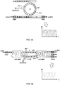
- FIGs 1A and 1B schematically illustrate examples of photonic sensors with periodic response behavior.
- FIG 1A illustrates an example of a ring resonator.
- FIG 1B illustrates an example of a multi-path interferometer, in this case a three-port Mach-Zehnder Interferometer (MZI).
- MZI Mach-Zehnder Interferometer
- the principle on which photonic sensors typically rely are changes of the effective refractive index n eff of the waveguide mode due to changes in the sample property "X" to be measured.
- the changes of the sample property can manifest in corresponding changes of its ambient refractive index n ambient , which can influence the effective refractive index n eff of the waveguide mode index e.g. via evanescent field interaction.
- ⁇ n eff ⁇ n eff ⁇ n ambient ⁇ n ambient
- the partial derivative may depend on parameters such as the wavelength and waveguide geometry.
- ⁇ res L R n eff ⁇ res m in which m is an integer called the mode number, e.g. the number of times the effective wavelength fits in the waveguide.
- the sensor transmission shows a sharp minimum or maximum at these resonance wavelengths, as shown in the plot of the signal S1 versus wavelength ⁇ .
- n g is the group index
- ⁇ neff is given by the equation above.
- Changes in the sample property X can be obtained from changes in the index n eff , which are obtained by measuring consecutive wavelength sweeps and identifying the shifts of the resonance wavelengths in these sweeps.
- the MZI has arms lengths which differ by an amount ⁇ L. Accordingly an increase in n eff will induce a larger phase difference ⁇ in the longer arm.
- an MZI can be implemented with equal arm lengths, where one of the arms is covered by a shielding layer. In such a configuration, the influence of temperature fluctuations is reduced since both arms will experience comparable refractive index change as the temperature changes.
- the phase sensitivity scales with ⁇ L allowing for a tunable high or low sensitivity, corresponding to a low or high range, respectively.
- the 3 ⁇ 3 MZI combines both arms with a 3 ⁇ 3 coupler resulting in three outputs that have a mutual 120 degrees phase difference. This can have advantages in readout.
- input light “"Li”” with an input wavelength ⁇ i is coupled into the photonic circuit, e.g. using a Vertical Grating Couplers (VGC) or other type coupler.
- Output light “"Lo”” may similarly be coupled out of the circuit.
- the output light “"Lo”” may comprise as respective signal S 1 or S 2 which may depend on the interaction between the sensor and the sample property "X”.
- the input wavelength ⁇ i is varied as function of time " t ", e.g. within a wavelength range ""R"".
- a broad spectrum input can be used and the output light spectrally resolved.
- the output signal S 1 may comprise information of the light intensity as a function of wavelength to determine characteristic signal values, e.g. the resonance dip or peak.
- the effective wavelength ⁇ eff in the ring-shaped waveguide may depend on the input wavelength ⁇ i (which is a function of time here) and the refractive index n eff in the waveguide (which depends on the sample property "X").
- the sample property "X" can be determined by keeping track of the position of a resonance wavelength ⁇ res which manifests as a dip in the intensity of the output signal here.
- the resonance wavelength ⁇ res may shift e.g. when the effective refractive index n eff in the waveguide shifts over time.
- the output signals S 2 comprise relative intensities which are a measure of the phase difference ⁇ between light paths, e.g. caused by a path length difference and/or difference in refractive index between paths. It is sufficient to measure the relative intensities only at one input wavelength ⁇ i to obtain the phase difference ⁇ .
- the phase shift can be retrieved at the same multiple wavelengths at which also the ring resonator transmission is measured.
- the equation contains three unknowns ( P 0 , V and ⁇ ), and three values P n so that each unknown can be solved for.
- the phase calculation is not sensitive to power or visibility variations.
- the 2-port implementation has zero sensitivity and ambiguous reading when the phase equals an integer times pi, which is not the case for the 3-port implementation.
- FSR free spectral range
- the experimental conditions using ring resonators are kept such that successive spectra do not shift by more than half an FSR, because in that case the actual shift may not be unambiguously determined.
- a similar problem may occur for other photonic sensors having periodic response such as the MZI. In the latter case, a phase shift of more than 2n may be ambiguous.
- the observed shift can be the actual shift plus or minus an integer times the FSR.
- FIGs 2A and 2B schematically illustrate different embodiments of a photonic circuit 10 comprising a low range sensor 11 and a high range sensor 12.
- the photonic circuit 10 comprises two ring resonators with the same or comparable circumference L R , but wherein one is partly shielded from the effects of the sample property "X" to obtain a lower sensitivity.
- the photonic circuit 10 comprises two ring resonators with the same or comparable circumference L R , but wherein one is partly shielded from the effects of the sample property "X" to obtain a lower sensitivity.
- the sample property "X" for example, by shielding a fraction F of the ring, only the remaining fraction (1-F) may be sensitive to the sample property "X".
- a change of the sample property may thus cause a lower wavelength shift in the shielded ring resonator than in the unshielded ring resonator, e.g. wherein the wavelength shift in the shielded ring resonator is a factor (1-F) times the wavelength shift in the unshielded ring resonator.
- the photonic circuit 10 comprises a combination of a ring resonator and an MZI.
- the resonance frequency ⁇ res of the ring resonator is determined by the ring circumference L R
- the phase shift ⁇ between the paths of the MZI is determined by the path length difference ⁇ L.
- the path length difference ⁇ L can be chosen relatively low to create a relatively low sensitivity or high range sensor 12. This is an advantage over a ring resonator which may not have arbitrarily low L R , since it has a minimum acceptable curvature below which light may start to leak from the waveguide.
- the refractive index of both the waveguides of the ring resonator and MZI may be similarly affected by the sample property "X" to cause a similar wavelength shift in the resonance frequency ⁇ res as in the wavelength position of a particular phase.
- the periodicity of the response can be different, e.g. wherein the MZI has a relatively long period compared to the FSR of the ring resonator.
- a period or wavelength interval between recurring signals is determined by a respective dimension of a waveguide forming the photonic sensor 11,12 and/or an effective wavelength of light traversing the waveguide.
- the wavelength interval between different recurrences or modes of a ring resonator can be determined by the circumference or path length L R of the waveguide forming a ring. Resonances typically occur at effective wavelengths ⁇ eff fitting an integer times into the ring path length L R .
- the wavelength interval between different recurrences or modes in an interferometer such as the MZI can be determined by the path length difference ⁇ L between arms of the interferometer.
- the same phase difference of light traveling the different arms typically occurs when the effective wavelength ⁇ eff fits an integer times into the path length difference ⁇ L .
- the effective wavelengths ⁇ eff can e.g. be varied by sweeping the wavelength ⁇ i of the input light "Li” and/or by changes of the effective refractive index n eff in the waveguide.
- the input light "Li" comprises a spectrum of multiple wavelengths measured simultaneously e.g. by a spectrometer.
- the path length difference ⁇ L is relatively small, e.g. comparable to or smaller than the effective wavelength ⁇ eff or input wavelength ⁇ i .
- a very low sensitivity or very high range sensor 12 can be formed wherein recurrences are far apart, e.g. sufficiently far to uniquely identify a mode number based on a particular phase difference in the second output signal S 2 .
- both paths can be the same length, e.g. wherein the effective refractive index n eff along one path has a different sensitivity to the sample property "X" than the other path.
- one path can be shielded.
- the shielding comprises a cover material with a thickness larger than a penetration depth of an evanescent field between the waveguide and sample.
- the wavelength interval of the high range sensor 12 may be larger than a wavelength ⁇ i of the input light Li to uniquely determine the mode number of the low range sensor 11 or provide an absolute (low sensitivity or high range) measurement of the sample property X.
- the photonic sensors 11,12 comprise two or more ring resonators 11,12 with equal path length L R , wherein one ring resonator 12 is made less sensitive to the sample property "X" than the other ring resonators 11.
- the high range sensor 12 is formed by a ring resonator covered by partial shielding. Accordingly, a relative sensitivity or range of the high range sensor 12 is determined by a fraction (1-F) that is unshielded.
- the relative sensitivity of the sensors 11,12 is determined by a relative amount of deposition of a sensor molecule on the surface of the ring resonators, wherein the sensor molecules bind to the sample "X" to be measured thereby changing the effective refractive index in the waveguide of the sensor.
- the photonic sensors 11,12 comprise a combination of a multi-path interferometer and a ring resonator, wherein the multi-path interferometer forms the high range sensor 12 by a relatively short path length difference ⁇ L between its different paths and the ring resonator forms the low range sensor 11 by to its relatively short long ring path length L R
- the path length difference may be implemented either as a physical length difference or, at the same physical length, as an intentionally designed effective index difference (for example using two different waveguide widths).
- a single input port "Pi" is used for coupling light into both the high and high range sensors.
- a sweeping input wavelength ⁇ i can also be used as input to the MZI, which is unconventional. This can have the advantage of more easily interrogating the device.
- different input ports can be used (not shown).
- a single output port Pt is used for coupling light out of the circuit.
- each ring resonator can have distinct resonance peaks.
- the photonic sensors comprise multiple low range or high sensitivity sensors working together with one high range or low sensitivity sensor.
- the high range sensor is used to calculate the mode number of a recurring signal in each of the low range sensors.
- the low range sensor need not all have the same sensitivity or range.
- a combination of two, three, four, or more sensors is used, wherein different sensors can have different ranges and/or sensitivities.
- one multi-path interferometer preferably an MZI employing at least one 3x3 MMI, may act as a high range sensor to distinguish recurring signal values in a plurality of low range ring resonators, having the same or different sensitivities. Because of the small size of the ring resonators compared to the multi-path interferometer, the combination may provide a large number of sensors on a relatively small foot print while distinguishing recurring signal values of the ring resonators.
- One embodiment for measuring a sample property "X" by means of photonic circuit 10 comprises applying input light “Li” into the photonic circuit 10 and measuring output light “Lo” out of the photonic circuit 10.
- the photonic sensors 11,12 are configured to modulate an intensity of the output light “Lo” with respect to the input light “Li” depending on the wavelength ⁇ i .
- the photonic circuit 10 comprises at least two photonic sensors 11,12 configured to modulate the output light "Lo” with respect to the input light “Li” according to a respective output signal S 1 ,S 2 .
- FIGs 3 and 4 schematically illustrate processing a combination of output signals S 1 , S 2 . from sensors having low range and high range to a particular sample property "X".
- FIG 4 schematically illustrates processing output signals S 1 ,S 2 in an embodiment with sensors having the different wavelength interval ⁇ 1 ⁇ 2 but the same or similar wavelength shifts ⁇ 1 and ⁇ 2 . in reaction to a given change ⁇ X of the sample property "X”. Such signals may e.g. occur in an embodiment as described with reference to FIG 2B .
- respective signal values V 1 ,V 2 of the respective output signals S 1 , S 2 may periodically recur as a function of a wavelength ⁇ i of the input light "Li" according to a respective wavelength interval ⁇ 1 , ⁇ 2 . Furthermore, if the sensors are affected by the sample property "X", a wavelength at which the recurring signal values V 1 , V 2 occur, may shift according to a respective wavelength shift ⁇ 1 , ⁇ 2 as a function of change ⁇ X in the sample property "X".
- the respective resonance wavelength ⁇ a , ⁇ b of a particular mode m a ,m a-1 , m a-2 may shift according to a change ⁇ X between initial sample property X[0] at the upper graph and the subsequent sample property X[t] in the graph there below.
- the resonance wavelength ⁇ res ,0 , and the wavelength ⁇ ⁇ 0 at which a particular phase ⁇ 0 is registered may shift according to the change ⁇ X between initial sample property X[0] at the upper graph and the subsequent sample property X[t] in the graph there below.
- two or more photonic sensors may be combined, each having at least some sensitivity to the same sample property "X" but to a different degree.
- the sensors 11,12 are relatively close together, e.g. within a distance of ten millimeter, one millimeter, hundred micrometer, or less.
- the sensors comprise a high range sensor 12 for measuring changes ⁇ X of the sample property "X" over a relatively high range.
- the high range sensor 12 may complement a low range sensor 11 having a relatively low range for measuring the same changes ⁇ X of the sample property "X", typically with a relatively high sensitivity.
- the sensitivity of the low range sensor 11 is relatively high and the sensitivity of the high range sensor 12 is relatively low.
- the second wavelength shift ⁇ 2 of the high range sensor 12 is smaller than the first wavelength shift ⁇ 1 of the low range sensor 11, e.g. by factor two, four, ten, twenty, or more (for the same change ⁇ X of the sample property X).
- a change of the (average) effective refractive index n eff resulting from a change ⁇ X of the sample property "X" is lower in the high range sensor 12 than in the low range sensor 11.
- the measurement resolution of the low range sensor 11 is better than that of the high range sensor 12. For example, a minimal difference that can be distinguished in measurement values corresponding to a particular (changes of) the sample property X are smaller in the low range sensor 11 than in the high range sensor 12.
- the second wavelength interval ⁇ 2 of the high range sensor 12 is larger than the first wavelength interval ⁇ 1 of the low range sensor 11, e.g. by factor two, four, ten, twenty, or more.
- a free spectral range FSR of the high range sensor 12 is larger than a free spectral range of the low range sensor 11. Also combinations of sensors with different wavelength intervals and different wavelength periods are possible.
- the low range sensor is a high-sensitivity sensor having a periodic response to the change of the sample property. This may cause (realistic) sample property changes to result in sensor response changes larger than the periodicity.
- the low range sensor, as described herein is a relatively low or reduced-sensitivity sensor, which may or may not have a periodic response to the change of the sample property, such that the sample property changes result in non-ambiguous sensor response changes.
- ⁇ X max ⁇ S
- A the sensor periodicity
- S the sensor transfer function efficiency.
- the quotient ⁇ 2 /S 2 of the high range sensor 12 is more than the quotient ⁇ 1 /S 1 of the low range sensor 11, e.g. by factor two, four, ten, twenty, or more.
- the phase sensitivity ⁇ is typically determined by the read-out hardware and/or software and the signal-to-noise ratio, and typically independent of the MZI design parameters such as the Free Spectral Range. Consequently, a good sensitivity (small ⁇ X) is in this case associated with a small unambiguous range ⁇ X max ,
- the sensitivity scales with the periodicity A, which is a ring resonator design parameter, so that a considerable unambiguous range ⁇ X max can be obtained even at a small ⁇ X.
- the sample property "X" is calculated by combining the output signals S 1 ,S 2 of the at least two photonic sensors 11,12.
- the second output signal S 2 of the high range sensor 12 can be used to distinguish between recurring signal values V 1 in the first output signal S 1 of the low range sensor 11.
- the resonance wavelength ⁇ a of the low range sensor 11 may have several recurrences of the same value for different modes m a-1 , m a , m a+1 .
- the recurrences can be distinguished using the resonance wavelength ⁇ b of the additional high range sensor 12.
- the photonic sensors 11,12 are calibrated to identify, by measurement of the second output signal S 2 , a mode number m a-1 ,m a ,m a-1 of a recurring signal value V 1 in the first output signal S 1 .
- an actual wavelength ⁇ a [t] or ⁇ res [t] of the recurring signal value V 1 in a particular number mode m a is calculated by measuring one wavelength ⁇ a+1 [t] or ⁇ ' res [t] at which the recurring signal value V 1 occurs in a measured wavelength range "R" of the first output signal S 1 and adding an integer number M times the wavelength interval ⁇ 1 of the low range sensor 11.
- the integer number M is based on the wavelength ⁇ b [t] at which a particular signal value V 2 in the second output signal S 2 occurs.
- the integer number M is based on a phase ⁇ t of the second output signal S 2 , e.g. at a particular wavelength ⁇ ⁇ t.
- the sample property "X" is calculated based on a difference of the output signal S 1 ,S 2 compared to a reference property X[0].
- a current sample property X[t] is calculated based on a difference between a current set of output signals S 1 ,S 2 corresponding to the current sample property "X” and a reference set of output signals S 1 ',S 2 ' corresponding to a reference sample property X[0].
- the sample property "X" is measured as a function of time "t”.
- differences in the output signals are correlated to differences in the refractive index n0,nt at different times and corresponding differences of the sample property "X" as a function of time "t".
- the sample property "X" is calculated based on a wavelength shift ⁇ 1 , ⁇ 2 of an identifiable signal value V 1, V 2 in the output signals S 1 ,S 2 compared to the reference sample property X[0].
- the identifiable signal value V 1 ,V 2 comprises a lowest signal value of a resonance peak or a particular phase of the output signal S 1 ,S 2 .
- the sample property "X" rapidly changes between subsequent measurements X[0],X[t] such that a wavelength ⁇ res of the recurrences in the first output signal S 1 shift more than half the wavelength interval ⁇ 1 of the low range sensor 11.
- relatively large changes of refractive index may occur over a short time when the photonic circuit 10 is put in a different medium, e.g. different media to be measured or from air into a liquid medium.
- the high range sensor 12 is sufficiently insensitive to the changing sample property "X" such that a change in mode number M of a recurrences in the first output signal S 1 can be identified.
- comparative measurements X[0],X[t] of the second output signal S 2 are kept within range of the second wavelength interval ⁇ 2 of the high range sensor 12, more preferably less than half the second wavelength interval ⁇ 2 .
- a wavelength shift ⁇ 2 in the second output signal S 2 of subsequent measurement X[0],X[t] is less than the wavelength interval ⁇ 2 of the high range sensor 12.
- a phase shift ⁇ in the second output signal S 2 of subsequent measurement X[0],X[t] is less than a full period 2n of the high range sensor 12.
- FIG 5 schematically illustrates a system 100 for measuring a sample property "X" by means of a photonic circuit 10.
- the system 100 comprises an optical interrogator 21,22 configured to apply input light "Li” into the photonic circuit 10 and measure output light “Lo” out of the photonic circuit 10.
- the photonic circuit 10 comprising two or more photonic sensors.
- the photonic sensors are configured to modulate the output light “Lo” with respect to the input light “Li” according to a respective output signal S 1 ,S 2 .
- Respective signal values of the respective output signals S 1 ,S 2 periodically recur as a function of a wavelength ⁇ i of the input light "Li” according to a respective wavelength interval ⁇ 1 , ⁇ 2 .
- the photonic circuit 10 comprises at least a low range sensor 11 having relatively low range to the change ⁇ X of the sample property "X” and a high range sensor 12 having relatively high range to the change ⁇ X of the sample property "X".
- the system 100 may comprise a controller 30 to perform operational acts in accordance with the methods as described herein.
- the controller 30 is configured or programmed to calculate the sample property "X" by combining the output signals S 1 ,S 2 of the at least two photonic sensors 11,12.
- the second output signal S 2 of the high range sensor 12 is used to distinguish between recurring signal values in the first output signal S 1 of the low range sensor 11.
- the system 100 comprises a light source 21 configured to direct the input light "Li” into the photonic circuit 10.
- the system 100 comprises a light sensor 22 configured to measure the output light "Lo” from the photonic circuit 10.
- the system 100 comprises a wavelength control unit 31 configured to set a wavelength of the input light "Li”.
- the controller 30 comprises signal processors 32-38 to determine the sample property from the signals S1,S2. While the processors are illustrated as separate blocks, some or all of their functionality can be integrated or combined.
- the signal processor 32 is configured to process the first output signal S 1 for determining a perceived wavelength ⁇ ' res,t of a recurring signal value, e.g. resonance dip.
- the signal processor 33 is configured to calculate a perceived wavelength shift ⁇ res ⁇ M ⁇ 1 based on the perceived wavelength ⁇ 'r es,t and a reference wavelength ⁇ res ,0 .
- the signal processor 34 is configured to process the second output signal S 2 for determining the second signal value V 2 e.g. phase ⁇ t.
- the signal processor 35 is configured to calculate a mode number M based on the second output signal S 2 e.g. by comparing the phase ⁇ t to a reference ⁇ 0 .
- the signal processor 36 configured to calculate an actual wavelength shift ⁇ res based on the perceived wavelength shift ⁇ res ⁇ M ⁇ 1 in the first output signal S 1 and the mode number M based on the second output signal S 2 .
- the signal processor 37 is configured to calculate a change ⁇ X in the sample property "X" based on the actual wavelength shift ⁇ res and e.g. a calibration constant Cx, function, or lookup table.
- the signal processor 38 is configured to calculate the sample property X[t] based on a reference value X[0] and the change ⁇ X.
- the signal processors or other parts of the system may be implemented in hardware or software.
- the present disclosure may be embodied as a non-transitory computer readable medium comprising software instructions that when executed on a computer, cause the execution of a method as described herein
Landscapes
- Chemical & Material Sciences (AREA)
- Physics & Mathematics (AREA)
- General Health & Medical Sciences (AREA)
- Life Sciences & Earth Sciences (AREA)
- Analytical Chemistry (AREA)
- Biochemistry (AREA)
- Health & Medical Sciences (AREA)
- General Physics & Mathematics (AREA)
- Immunology (AREA)
- Pathology (AREA)
- Engineering & Computer Science (AREA)
- Chemical Kinetics & Catalysis (AREA)
- Plasma & Fusion (AREA)
- Investigating Or Analysing Materials By Optical Means (AREA)
Claims (14)
- Verfahren zum Messen einer Abtasteigenschaft (X) mittels einer photonischen Schaltung (10), wobei das Verfahren umfasst- Anlegen von Eingangslicht (Li) an die photonische Schaltung (10) und Messen von Ausgangslicht (Lo) aus der photonischen Schaltung (10);- wobei die photonische Schaltung (10) wenigstens zwei photonische Sensoren (11, 12) umfasst, die konfiguriert sind, um das Ausgangslicht (Lo) in Bezug auf das Eingangslicht (Li) nach einem jeweiligen Ausgangssignal (S1, S2) interferometrisch zu modulieren;- wobei die jeweiligen Signalwerte (V1V2) der jeweiligen Ausgangssignale (S1,S2) periodisch als Funktion einer Wellenlänge (λi) des Eingangslichts (Li) nach einem jeweiligen Wellenlängenintervall (Λ1,Λ2) wiederkehren;- wobei sich eine Wellenlänge (λa,λb), bei der die wiederkehrenden Signalwerte (V1,V2) auftreten, entsprechend einer jeweiligen Wellenlängenverschiebung (Δλ1,Δλ2) als Funktion der Änderung (ΔX) in der zu messenden Abtasteigenschaft (X) durch eine entsprechende Änderung des effektiven Brechungsindex für das Licht durch wenigstens einen Teil der photonischen Sensoren (11,12) verschiebt;- wobei ein relativer Bereich eines jeweiligen photonischen Sensors (11,12) für die Abtasteigenschaft (X) durch einen jeweiligen Quotienten (λ1/Aλ1, Λ2/Δλ2) des jeweiligen Wellenlängenintervalls (Λ1,Λ2) über die jeweilige Wellenlängenverschiebung (Δλ1, Δλ2) für eine Änderung (ΔX) der Abtasteigenschaft (X) definiert wird;- wobei die wenigstens zwei photonischen Sensoren (11,12) einen Niederbereichssensor (11) umfassen, der ein erstes Ausgangssignal (S1) bereitstellt, und einen Hochbereichssensor (12), der ein zweites Ausgangssignal (S2) bereitstellt, wobei der Hochbereichssensor (12) einen höheren relativen Bereich für die Abtasteigenschaft (X) als der Niederbereichssensor (11) hat;- wobei die Abtasteigenschaft (X) durch Kombinieren der Ausgangssignale (S1,S2) der wenigstens zwei photonischen Sensoren (11,12) berechnet wird, wobei das zweite Ausgangssignal (S2) des Hochbereichssensors (12) verwendet wird, um zwischen wiederkehrenden Signalwerten (V1) im ersten Ausgangssignal (S1) des Niederbereichssensors (11) zu unterscheiden,dadurch gekennzeichnet, dass die photonischen Sensoren (11,12) eine Kombination aus einem Mehrweginterferometer und einem Ringresonator umfassen, wobei das Mehrweginterferometer den Hochbereichssensor (12) und der Ringresonator den Niederbereichssensor (11) bildet.
- Verfahren nach Anspruch 1, wobei die photonischen Sensoren (11, 12) kalibriert sind, um durch Messung des zweiten Ausgangssignals (S2) eine Modennummer (ma-1,ma,ma-1) von einem wiederkehrenden Signalwert (V1) im ersten Ausgangssignal (S1) zu identifizieren.
- Verfahren nach einem der vorhergehenden Ansprüche, wobei eine tatsächliche Wellenlänge (λa[t]) oder eine tatsächliche Verschiebung der Wellenlänge (Δλ1) des wiederkehrenden Signalwerts (V1) in einem bestimmten Zahlenmodus (ma) durch Messen einer Wellenlänge (λa+1[t]) berechnet wird, bei der der wiederkehrende Signalwert (V1) in einem gemessenen Wellenlängenbereich (R) des ersten Ausgangssignals (S1) auftritt, und Hinzufügen einer Ganzzahl (M) mal dem Wellenlängenintervall (Λ1) des Niederbereichssensors (11), wobei die Ganzzahl (M) auf dem zweiten Ausgangssignal (S2) basiert.
- Verfahren nach einem der vorhergehenden Ansprüche, wobei die Abtasteigenschaft (X) basierend auf einer Differenz des Ausgangssignals (S1,S2) im Vergleich zu einer Referenzeigenschaft (X[0]) berechnet wird.
- Verfahren nach einem der vorhergehenden Ansprüche, wobei die Abtasteigenschaft (X) basierend auf einer Wellenlängenverschiebung (Δλ1, Δλ2) eines identifizierbaren Signalwerts (V1, V2) in den Ausgangssignalen (S1,S2) im Vergleich zur Eigenschaft der Referenzabtasteigenschaft (X[0]) berechnet wird.
- Verfahren nach einem der vorhergehenden Ansprüche, wobei sich die Abtasteigenschaft (X) zwischen nachfolgenden Messungen (X[0],X[t]) schnell ändert, so dass sich eine Wellenlänge (λres) der Wiederholungen in dem ersten Ausgangssignal (S1) um mehr als die Hälfte des Wellenlängenintervalls (Λ1) des Niederbereichssensors (11) verschiebt, wobei der Hochbereichssensor (12) gegenüber der sich ändernden Abtasteigenschaft (X) ausreichend unempfindlich ist, so dass eine Änderung der Modennummer (M) von Wiederholungen im ersten Ausgangssignal (S1) identifiziert werden kann.
- Verfahren nach einem der vorhergehenden Ansprüche, wobei das jeweilige Wellenlängenintervall (Λ1,Λ2) durch eine jeweilige Abmessung (LR,ΔL) eines Wellenleiters bestimmt wird, der den photonischen Sensor (11, 12) und/oder eine effektive Wellenlänge (λeff) des Lichts bildet, das den Wellenleiter durchquert.
- Verfahren nach einem der vorhergehenden Ansprüche, wobei das Wellenlängenintervall (Λ2) des Hochbereichssensors (12) größer als eine Wellenlänge (λi) des Eingangslichts (Li) ist
- Verfahren nach einem der vorhergehenden Ansprüche, wobei die photonischen Sensoren (11,12) zwei oder mehr Ringresonatoren (11,12) mit gleicher Weglänge (LR) umfassen, wobei ein Ringresonator (12) weniger empfindlich gegenüber der Abtasteigenschaft (X) als die anderen Ringresonatoren (11) gemacht wird.
- Verfahren nach einem der vorhergehenden Ansprüche, wobei die photonischen Sensoren mehrere Niederbereichssensoren umfassen, die mit einem Hochbereichssensor zusammenarbeiten, wobei der Hochbereichssensor verwendet wird, um die Modennummer eines wiederkehrenden Signals in jedem der Niederbereichssensoren zu berechnen.
- Verfahren nach einem der vorhergehenden Ansprüche, wobei die photonischen Sensoren (11, 12) konfiguriert sind, um eine Intensität des Ausgangslichts (Lo) in Bezug auf das Eingangslicht (Li) in Abhängigkeit von der Wellenlänge (λ1) zu modulieren.
- Verfahren nach einem der vorhergehenden Ansprüche, wobei der Quotient (Λ2/Δλ2), der den relativen Bereich des Hochbereichssensors (12) für die Abtasteigenschaft (X) angibt, höher ist als der Quotient (Δ1/Δλ1), der den relativen Bereich des Niederbereichssensors (11) für die Abtasteigenschaft (X) um wenigstens den Faktor zehn angibt.
- Ein nicht flüchtiges computerlesbares Medium, das Softwareanweisungen umfasst, die, wenn sie auf einem Computer ausgeführt werden, die Ausführung eines Verfahrens nach einem der vorhergehenden Ansprüche bewirken.
- System (100) zum Messen einer Abtasteigenschaft (X) mittels einer photonischen Schaltung (10), wobei das System (100) umfasst- einen optischen Interrogator (21, 22), der konfiguriert ist, um Eingangslicht (Li) in die photonische Schaltung (10) anzulegen und Ausgangslicht (Lo) aus der photonischen Schaltung (10) heraus zu messen;- die photonische Schaltung (10), die wenigstens zwei photonische Sensoren (11, 12) umfasst; wobei die photonischen Sensoren (11,12) konfiguriert sind, um das Ausgangslicht (Lo) in Bezug auf das Eingangslicht (Li) nach einem jeweiligen Ausgangssignal (S1,S2) interferometrisch zu modulieren; wobei die jeweiligen Signalwerte (V1,V2) der jeweiligen Ausgangssignale (S1,S2) periodisch als Funktion einer Wellenlänge (λi) des Eingangslichts (Li) nach einem jeweiligen Wellenlängenintervall (Λ1, Λ2) wiederkehren; wobei sich eine Wellenlänge (λa,λb), bei der die wiederkehrenden Signalwerte (V1,V2) auftreten, entsprechend einer jeweiligen Wellenlängenverschiebung (Δλ1, Δλ2) als Funktion der Änderung (ΔX) in der zu messenden Abtasteigenschaft (X) durch eine entsprechende Änderung des effektiven Brechungsindex für das Licht durch wenigstens einen Teil der photonischen Sensoren (11,12) verschiebt; wobei ein relativer Bereich eines jeweiligen photonischen Sensors (11,12) für die Abtasteigenschaft (X) durch einen jeweiligen Quotienten (Λ1/Δλ1, Λ2/Δλ2) des jeweiligen Wellenlängenintervalls (Λ1,Λ2) über die jeweilige Wellenlängenverschiebung (Δλ1,Δλ2) für eine Änderung (ΔX) der Abtasteigenschaft (X) definiert ist; wobei die wenigstens zwei photonischen Sensoren (11,12) einen Niederbereichssensor (11) umfassen, der ein erstes Ausgangssignal (S1) bereitstellt, und einen Hochbereichssensor (12), der ein zweites Ausgangssignal (S2) bereitstellt, wobei der Hochbereichssensor (12) einen höheren relativen Bereich für die Abtasteigenschaft (X) als der Sensor für niedrigen Bereich (11) hat;- eine Steuerung (30), die konfiguriert ist, um die Abtasteigenschaft (X) durch Kombinieren der Ausgangssignale (S1,S2) der wenigstens zwei photonischen Sensoren (11,12) zu berechnen, wobei das zweite Ausgangssignal (S2) des Hochbereichssensors (12) verwendet wird, um zwischen wiederkehrenden Signalwerten (V1) im ersten Ausgangssignal (S1) des Niederbereichssensors (11) zu unterscheiden;dadurch gekennzeichnet, dass die photonischen Sensoren (11,12) eine Kombination aus einem Mehrweginterferometer und einem Ringresonator umfassen, wobei das Mehrweginterferometer den Hochbereichssensor (12) und der Ringresonator den Niederbereichssensor (11) bildet.
Applications Claiming Priority (3)
| Application Number | Priority Date | Filing Date | Title |
|---|---|---|---|
| EP17153868 | 2017-01-31 | ||
| EP17183545.7A EP3435069A1 (de) | 2017-07-27 | 2017-07-27 | Photonische schaltung zur messung einer probe |
| PCT/NL2018/050061 WO2018143797A1 (en) | 2017-01-31 | 2018-01-30 | Photonic circuit for measuring a sample |
Publications (2)
| Publication Number | Publication Date |
|---|---|
| EP3577439A1 EP3577439A1 (de) | 2019-12-11 |
| EP3577439B1 true EP3577439B1 (de) | 2020-12-09 |
Family
ID=61168146
Family Applications (1)
| Application Number | Title | Priority Date | Filing Date |
|---|---|---|---|
| EP18703644.7A Active EP3577439B1 (de) | 2017-01-31 | 2018-01-30 | Photonische schaltung zur messung einer probe |
Country Status (4)
| Country | Link |
|---|---|
| US (1) | US10794825B2 (de) |
| EP (1) | EP3577439B1 (de) |
| ES (1) | ES2864632T3 (de) |
| WO (1) | WO2018143797A1 (de) |
Families Citing this family (3)
| Publication number | Priority date | Publication date | Assignee | Title |
|---|---|---|---|---|
| US12153045B2 (en) | 2020-05-19 | 2024-11-26 | The Texas A&M University System | Mid-infrared integrated photonics for biological sensing |
| FR3129480B1 (fr) * | 2021-11-23 | 2023-10-06 | Commissariat Energie Atomique | système interferometrique de detection comportant des capteurs optiques de mesure et de réfErence de différentes sensibilités |
| WO2025006650A2 (en) * | 2023-06-26 | 2025-01-02 | University Of Rochester | Microphysiological system devices with self-contained photonic integrated circuit sensors |
Family Cites Families (6)
| Publication number | Priority date | Publication date | Assignee | Title |
|---|---|---|---|---|
| US20040023396A1 (en) * | 2001-11-14 | 2004-02-05 | Boyd Robert W. | Ring or disk resonator photonic biosensor and its use |
| EP2267432A1 (de) * | 2009-06-25 | 2010-12-29 | Nederlandse Organisatie voor toegepast -natuurwetenschappelijk onderzoek TNO | Optisches Sensorsystem |
| EP2270478B1 (de) | 2009-07-01 | 2012-03-28 | Fraunhofer-Gesellschaft zur Förderung der angewandten Forschung e.V. | Optischer Sensor und Verfahren zum Detektieren von Molekülen |
| GB201117649D0 (en) * | 2011-10-12 | 2011-11-23 | Univ Gent | Resonant biosensor |
| US9846060B2 (en) * | 2013-03-28 | 2017-12-19 | Frauhofer-Gesellschaft Zur Foerderung Der Angewandten Forschung E.V. | Optical sensor arrangement and method for measuring an observable |
| US9864144B2 (en) | 2015-02-04 | 2018-01-09 | Lionix International Bv | Multi-path interferometeric sensor |
-
2018
- 2018-01-30 US US16/478,954 patent/US10794825B2/en active Active
- 2018-01-30 EP EP18703644.7A patent/EP3577439B1/de active Active
- 2018-01-30 ES ES18703644T patent/ES2864632T3/es active Active
- 2018-01-30 WO PCT/NL2018/050061 patent/WO2018143797A1/en not_active Ceased
Non-Patent Citations (1)
| Title |
|---|
| None * |
Also Published As
| Publication number | Publication date |
|---|---|
| ES2864632T3 (es) | 2021-10-14 |
| WO2018143797A1 (en) | 2018-08-09 |
| EP3577439A1 (de) | 2019-12-11 |
| US20190353588A1 (en) | 2019-11-21 |
| US10794825B2 (en) | 2020-10-06 |
Similar Documents
| Publication | Publication Date | Title |
|---|---|---|
| US9864144B2 (en) | Multi-path interferometeric sensor | |
| US8823947B2 (en) | Optical sensor and method for detecting molecules | |
| CN105806380B (zh) | 一种基于长周期光纤光栅反射型传感器的复用解调设备 | |
| US8665447B2 (en) | Enhanced sensitivity interferometric sensors | |
| EP3577439B1 (de) | Photonische schaltung zur messung einer probe | |
| Zhou et al. | Simultaneous strain and temperature measurement with fiber Bragg grating and multimode fibers using an intensity-based interrogation method | |
| EP2267432A1 (de) | Optisches Sensorsystem | |
| CN111323059A (zh) | 基于光纤布拉格光栅法布里-泊罗腔的传感装置 | |
| US9068950B2 (en) | Vernier photonic sensor data-analysis | |
| CN102132129B (zh) | 光纤干涉仪及用于确定光纤干涉仪的光纤线圈内部的物理状态参数的方法 | |
| CN109374028B (zh) | 一种基于级联长周期光纤光栅的分布式复用解调系统 | |
| CN101187556A (zh) | 一种光纤测距方法及装置 | |
| Li et al. | Tilted fiber Bragg grating sensors based on time-domain measurements with microwave photonics | |
| KR101541602B1 (ko) | 저간섭성 광원과 분산형 간섭계를 이용한 다축 측정 광학 갭 센서 장치 및 광학 갭 센서를 이용한 다축 측정 광학 갭 센싱 방법 | |
| EP3435069A1 (de) | Photonische schaltung zur messung einer probe | |
| Milvich et al. | Mach-Zehnder interferometer readout for instantaneous sensor calibration and extraction of endlessly unwrapped phase | |
| Zhang et al. | Experimental investigation on optical spectral deformation of embedded FBG sensors | |
| Jones et al. | Multiplexing optical fiber sensors | |
| Demeter-Finzi et al. | Back-reflecting interferometeric sensor based on a single grating on a planar waveguide | |
| US20240183712A1 (en) | A spectral sensing system | |
| GB2419401A (en) | Polarimetric differential optical fibre sensor | |
| US20250164233A1 (en) | Demodulation system for optical fiber fabry-perot sensor | |
| Miridonov et al. | Digital demodulation algorithm for white-light fiber optic interferometric sensors | |
| CN111220187B (zh) | 基于低相干干涉原理的级联长周期光纤光栅复用解调装置 | |
| Valeev et al. | Refractive index sensing using addressed fiber Bragg structures with etched section |
Legal Events
| Date | Code | Title | Description |
|---|---|---|---|
| STAA | Information on the status of an ep patent application or granted ep patent |
Free format text: STATUS: UNKNOWN |
|
| STAA | Information on the status of an ep patent application or granted ep patent |
Free format text: STATUS: THE INTERNATIONAL PUBLICATION HAS BEEN MADE |
|
| PUAI | Public reference made under article 153(3) epc to a published international application that has entered the european phase |
Free format text: ORIGINAL CODE: 0009012 |
|
| STAA | Information on the status of an ep patent application or granted ep patent |
Free format text: STATUS: REQUEST FOR EXAMINATION WAS MADE |
|
| 17P | Request for examination filed |
Effective date: 20190801 |
|
| AK | Designated contracting states |
Kind code of ref document: A1 Designated state(s): AL AT BE BG CH CY CZ DE DK EE ES FI FR GB GR HR HU IE IS IT LI LT LU LV MC MK MT NL NO PL PT RO RS SE SI SK SM TR |
|
| AX | Request for extension of the european patent |
Extension state: BA ME |
|
| DAV | Request for validation of the european patent (deleted) | ||
| DAX | Request for extension of the european patent (deleted) | ||
| GRAP | Despatch of communication of intention to grant a patent |
Free format text: ORIGINAL CODE: EPIDOSNIGR1 |
|
| STAA | Information on the status of an ep patent application or granted ep patent |
Free format text: STATUS: GRANT OF PATENT IS INTENDED |
|
| INTG | Intention to grant announced |
Effective date: 20200626 |
|
| GRAS | Grant fee paid |
Free format text: ORIGINAL CODE: EPIDOSNIGR3 |
|
| GRAA | (expected) grant |
Free format text: ORIGINAL CODE: 0009210 |
|
| STAA | Information on the status of an ep patent application or granted ep patent |
Free format text: STATUS: THE PATENT HAS BEEN GRANTED |
|
| AK | Designated contracting states |
Kind code of ref document: B1 Designated state(s): AL AT BE BG CH CY CZ DE DK EE ES FI FR GB GR HR HU IE IS IT LI LT LU LV MC MK MT NL NO PL PT RO RS SE SI SK SM TR |
|
| REG | Reference to a national code |
Ref country code: GB Ref legal event code: FG4D |
|
| REG | Reference to a national code |
Ref country code: AT Ref legal event code: REF Ref document number: 1343934 Country of ref document: AT Kind code of ref document: T Effective date: 20201215 Ref country code: CH Ref legal event code: EP |
|
| REG | Reference to a national code |
Ref country code: DE Ref legal event code: R096 Ref document number: 602018010640 Country of ref document: DE |
|
| REG | Reference to a national code |
Ref country code: IE Ref legal event code: FG4D |
|
| REG | Reference to a national code |
Ref country code: NL Ref legal event code: FP |
|
| PG25 | Lapsed in a contracting state [announced via postgrant information from national office to epo] |
Ref country code: FI Free format text: LAPSE BECAUSE OF FAILURE TO SUBMIT A TRANSLATION OF THE DESCRIPTION OR TO PAY THE FEE WITHIN THE PRESCRIBED TIME-LIMIT Effective date: 20201209 Ref country code: RS Free format text: LAPSE BECAUSE OF FAILURE TO SUBMIT A TRANSLATION OF THE DESCRIPTION OR TO PAY THE FEE WITHIN THE PRESCRIBED TIME-LIMIT Effective date: 20201209 Ref country code: NO Free format text: LAPSE BECAUSE OF FAILURE TO SUBMIT A TRANSLATION OF THE DESCRIPTION OR TO PAY THE FEE WITHIN THE PRESCRIBED TIME-LIMIT Effective date: 20210309 Ref country code: GR Free format text: LAPSE BECAUSE OF FAILURE TO SUBMIT A TRANSLATION OF THE DESCRIPTION OR TO PAY THE FEE WITHIN THE PRESCRIBED TIME-LIMIT Effective date: 20210310 |
|
| REG | Reference to a national code |
Ref country code: AT Ref legal event code: MK05 Ref document number: 1343934 Country of ref document: AT Kind code of ref document: T Effective date: 20201209 |
|
| PG25 | Lapsed in a contracting state [announced via postgrant information from national office to epo] |
Ref country code: SE Free format text: LAPSE BECAUSE OF FAILURE TO SUBMIT A TRANSLATION OF THE DESCRIPTION OR TO PAY THE FEE WITHIN THE PRESCRIBED TIME-LIMIT Effective date: 20201209 Ref country code: LV Free format text: LAPSE BECAUSE OF FAILURE TO SUBMIT A TRANSLATION OF THE DESCRIPTION OR TO PAY THE FEE WITHIN THE PRESCRIBED TIME-LIMIT Effective date: 20201209 Ref country code: BG Free format text: LAPSE BECAUSE OF FAILURE TO SUBMIT A TRANSLATION OF THE DESCRIPTION OR TO PAY THE FEE WITHIN THE PRESCRIBED TIME-LIMIT Effective date: 20210309 |
|
| PG25 | Lapsed in a contracting state [announced via postgrant information from national office to epo] |
Ref country code: HR Free format text: LAPSE BECAUSE OF FAILURE TO SUBMIT A TRANSLATION OF THE DESCRIPTION OR TO PAY THE FEE WITHIN THE PRESCRIBED TIME-LIMIT Effective date: 20201209 |
|
| REG | Reference to a national code |
Ref country code: LT Ref legal event code: MG9D |
|
| PG25 | Lapsed in a contracting state [announced via postgrant information from national office to epo] |
Ref country code: SM Free format text: LAPSE BECAUSE OF FAILURE TO SUBMIT A TRANSLATION OF THE DESCRIPTION OR TO PAY THE FEE WITHIN THE PRESCRIBED TIME-LIMIT Effective date: 20201209 Ref country code: SK Free format text: LAPSE BECAUSE OF FAILURE TO SUBMIT A TRANSLATION OF THE DESCRIPTION OR TO PAY THE FEE WITHIN THE PRESCRIBED TIME-LIMIT Effective date: 20201209 Ref country code: EE Free format text: LAPSE BECAUSE OF FAILURE TO SUBMIT A TRANSLATION OF THE DESCRIPTION OR TO PAY THE FEE WITHIN THE PRESCRIBED TIME-LIMIT Effective date: 20201209 Ref country code: CZ Free format text: LAPSE BECAUSE OF FAILURE TO SUBMIT A TRANSLATION OF THE DESCRIPTION OR TO PAY THE FEE WITHIN THE PRESCRIBED TIME-LIMIT Effective date: 20201209 Ref country code: LT Free format text: LAPSE BECAUSE OF FAILURE TO SUBMIT A TRANSLATION OF THE DESCRIPTION OR TO PAY THE FEE WITHIN THE PRESCRIBED TIME-LIMIT Effective date: 20201209 Ref country code: PT Free format text: LAPSE BECAUSE OF FAILURE TO SUBMIT A TRANSLATION OF THE DESCRIPTION OR TO PAY THE FEE WITHIN THE PRESCRIBED TIME-LIMIT Effective date: 20210409 Ref country code: RO Free format text: LAPSE BECAUSE OF FAILURE TO SUBMIT A TRANSLATION OF THE DESCRIPTION OR TO PAY THE FEE WITHIN THE PRESCRIBED TIME-LIMIT Effective date: 20201209 |
|
| PG25 | Lapsed in a contracting state [announced via postgrant information from national office to epo] |
Ref country code: AT Free format text: LAPSE BECAUSE OF FAILURE TO SUBMIT A TRANSLATION OF THE DESCRIPTION OR TO PAY THE FEE WITHIN THE PRESCRIBED TIME-LIMIT Effective date: 20201209 Ref country code: PL Free format text: LAPSE BECAUSE OF FAILURE TO SUBMIT A TRANSLATION OF THE DESCRIPTION OR TO PAY THE FEE WITHIN THE PRESCRIBED TIME-LIMIT Effective date: 20201209 |
|
| REG | Reference to a national code |
Ref country code: CH Ref legal event code: PL |
|
| REG | Reference to a national code |
Ref country code: DE Ref legal event code: R097 Ref document number: 602018010640 Country of ref document: DE |
|
| PG25 | Lapsed in a contracting state [announced via postgrant information from national office to epo] |
Ref country code: MC Free format text: LAPSE BECAUSE OF FAILURE TO SUBMIT A TRANSLATION OF THE DESCRIPTION OR TO PAY THE FEE WITHIN THE PRESCRIBED TIME-LIMIT Effective date: 20201209 Ref country code: IS Free format text: LAPSE BECAUSE OF FAILURE TO SUBMIT A TRANSLATION OF THE DESCRIPTION OR TO PAY THE FEE WITHIN THE PRESCRIBED TIME-LIMIT Effective date: 20210409 Ref country code: LU Free format text: LAPSE BECAUSE OF NON-PAYMENT OF DUE FEES Effective date: 20210130 |
|
| REG | Reference to a national code |
Ref country code: BE Ref legal event code: MM Effective date: 20210131 |
|
| REG | Reference to a national code |
Ref country code: ES Ref legal event code: FG2A Ref document number: 2864632 Country of ref document: ES Kind code of ref document: T3 Effective date: 20211014 |
|
| PLBE | No opposition filed within time limit |
Free format text: ORIGINAL CODE: 0009261 |
|
| STAA | Information on the status of an ep patent application or granted ep patent |
Free format text: STATUS: NO OPPOSITION FILED WITHIN TIME LIMIT |
|
| PG25 | Lapsed in a contracting state [announced via postgrant information from national office to epo] |
Ref country code: IT Free format text: LAPSE BECAUSE OF FAILURE TO SUBMIT A TRANSLATION OF THE DESCRIPTION OR TO PAY THE FEE WITHIN THE PRESCRIBED TIME-LIMIT Effective date: 20201209 Ref country code: AL Free format text: LAPSE BECAUSE OF FAILURE TO SUBMIT A TRANSLATION OF THE DESCRIPTION OR TO PAY THE FEE WITHIN THE PRESCRIBED TIME-LIMIT Effective date: 20201209 |
|
| 26N | No opposition filed |
Effective date: 20210910 |
|
| PG25 | Lapsed in a contracting state [announced via postgrant information from national office to epo] |
Ref country code: LI Free format text: LAPSE BECAUSE OF NON-PAYMENT OF DUE FEES Effective date: 20210131 Ref country code: DK Free format text: LAPSE BECAUSE OF FAILURE TO SUBMIT A TRANSLATION OF THE DESCRIPTION OR TO PAY THE FEE WITHIN THE PRESCRIBED TIME-LIMIT Effective date: 20201209 Ref country code: CH Free format text: LAPSE BECAUSE OF NON-PAYMENT OF DUE FEES Effective date: 20210131 Ref country code: SI Free format text: LAPSE BECAUSE OF FAILURE TO SUBMIT A TRANSLATION OF THE DESCRIPTION OR TO PAY THE FEE WITHIN THE PRESCRIBED TIME-LIMIT Effective date: 20201209 |
|
| PG25 | Lapsed in a contracting state [announced via postgrant information from national office to epo] |
Ref country code: IE Free format text: LAPSE BECAUSE OF NON-PAYMENT OF DUE FEES Effective date: 20210130 |
|
| PG25 | Lapsed in a contracting state [announced via postgrant information from national office to epo] |
Ref country code: IS Free format text: LAPSE BECAUSE OF FAILURE TO SUBMIT A TRANSLATION OF THE DESCRIPTION OR TO PAY THE FEE WITHIN THE PRESCRIBED TIME-LIMIT Effective date: 20210409 |
|
| PG25 | Lapsed in a contracting state [announced via postgrant information from national office to epo] |
Ref country code: BE Free format text: LAPSE BECAUSE OF NON-PAYMENT OF DUE FEES Effective date: 20210131 |
|
| P01 | Opt-out of the competence of the unified patent court (upc) registered |
Effective date: 20230522 |
|
| PG25 | Lapsed in a contracting state [announced via postgrant information from national office to epo] |
Ref country code: CY Free format text: LAPSE BECAUSE OF FAILURE TO SUBMIT A TRANSLATION OF THE DESCRIPTION OR TO PAY THE FEE WITHIN THE PRESCRIBED TIME-LIMIT Effective date: 20201209 |
|
| PG25 | Lapsed in a contracting state [announced via postgrant information from national office to epo] |
Ref country code: HU Free format text: LAPSE BECAUSE OF FAILURE TO SUBMIT A TRANSLATION OF THE DESCRIPTION OR TO PAY THE FEE WITHIN THE PRESCRIBED TIME-LIMIT; INVALID AB INITIO Effective date: 20180130 |
|
| PG25 | Lapsed in a contracting state [announced via postgrant information from national office to epo] |
Ref country code: MK Free format text: LAPSE BECAUSE OF FAILURE TO SUBMIT A TRANSLATION OF THE DESCRIPTION OR TO PAY THE FEE WITHIN THE PRESCRIBED TIME-LIMIT Effective date: 20201209 |
|
| PG25 | Lapsed in a contracting state [announced via postgrant information from national office to epo] |
Ref country code: MT Free format text: LAPSE BECAUSE OF FAILURE TO SUBMIT A TRANSLATION OF THE DESCRIPTION OR TO PAY THE FEE WITHIN THE PRESCRIBED TIME-LIMIT Effective date: 20201209 |
|
| PG25 | Lapsed in a contracting state [announced via postgrant information from national office to epo] |
Ref country code: TR Free format text: LAPSE BECAUSE OF FAILURE TO SUBMIT A TRANSLATION OF THE DESCRIPTION OR TO PAY THE FEE WITHIN THE PRESCRIBED TIME-LIMIT Effective date: 20201209 |
|
| PGFP | Annual fee paid to national office [announced via postgrant information from national office to epo] |
Ref country code: NL Payment date: 20260121 Year of fee payment: 9 |
|
| PGFP | Annual fee paid to national office [announced via postgrant information from national office to epo] |
Ref country code: GB Payment date: 20260123 Year of fee payment: 9 |
|
| PGFP | Annual fee paid to national office [announced via postgrant information from national office to epo] |
Ref country code: ES Payment date: 20260227 Year of fee payment: 9 |
|
| PGFP | Annual fee paid to national office [announced via postgrant information from national office to epo] |
Ref country code: DE Payment date: 20260121 Year of fee payment: 9 |
|
| PGFP | Annual fee paid to national office [announced via postgrant information from national office to epo] |
Ref country code: FR Payment date: 20260123 Year of fee payment: 9 |