EP3576170A1 - Illumination device and method for manufacturing said illumination device - Google Patents
Illumination device and method for manufacturing said illumination device Download PDFInfo
- Publication number
- EP3576170A1 EP3576170A1 EP18745218.0A EP18745218A EP3576170A1 EP 3576170 A1 EP3576170 A1 EP 3576170A1 EP 18745218 A EP18745218 A EP 18745218A EP 3576170 A1 EP3576170 A1 EP 3576170A1
- Authority
- EP
- European Patent Office
- Prior art keywords
- illumination device
- base layer
- light source
- reflective layer
- conductors
- Prior art date
- Legal status (The legal status is an assumption and is not a legal conclusion. Google has not performed a legal analysis and makes no representation as to the accuracy of the status listed.)
- Withdrawn
Links
Images





Classifications
-
- H—ELECTRICITY
- H10—SEMICONDUCTOR DEVICES; ELECTRIC SOLID-STATE DEVICES NOT OTHERWISE PROVIDED FOR
- H10H—INORGANIC LIGHT-EMITTING SEMICONDUCTOR DEVICES HAVING POTENTIAL BARRIERS
- H10H20/00—Individual inorganic light-emitting semiconductor devices having potential barriers, e.g. light-emitting diodes [LED]
- H10H20/80—Constructional details
- H10H20/85—Packages
- H10H20/855—Optical field-shaping means, e.g. lenses
- H10H20/856—Reflecting means
-
- F—MECHANICAL ENGINEERING; LIGHTING; HEATING; WEAPONS; BLASTING
- F21—LIGHTING
- F21S—NON-PORTABLE LIGHTING DEVICES; SYSTEMS THEREOF; VEHICLE LIGHTING DEVICES SPECIALLY ADAPTED FOR VEHICLE EXTERIORS
- F21S2/00—Systems of lighting devices, not provided for in main groups F21S4/00 - F21S10/00 or F21S19/00, e.g. of modular construction
-
- F—MECHANICAL ENGINEERING; LIGHTING; HEATING; WEAPONS; BLASTING
- F21—LIGHTING
- F21V—FUNCTIONAL FEATURES OR DETAILS OF LIGHTING DEVICES OR SYSTEMS THEREOF; STRUCTURAL COMBINATIONS OF LIGHTING DEVICES WITH OTHER ARTICLES, NOT OTHERWISE PROVIDED FOR
- F21V19/00—Fastening of light sources or lamp holders
-
- F—MECHANICAL ENGINEERING; LIGHTING; HEATING; WEAPONS; BLASTING
- F21—LIGHTING
- F21V—FUNCTIONAL FEATURES OR DETAILS OF LIGHTING DEVICES OR SYSTEMS THEREOF; STRUCTURAL COMBINATIONS OF LIGHTING DEVICES WITH OTHER ARTICLES, NOT OTHERWISE PROVIDED FOR
- F21V23/00—Arrangement of electric circuit elements in or on lighting devices
-
- F—MECHANICAL ENGINEERING; LIGHTING; HEATING; WEAPONS; BLASTING
- F21—LIGHTING
- F21V—FUNCTIONAL FEATURES OR DETAILS OF LIGHTING DEVICES OR SYSTEMS THEREOF; STRUCTURAL COMBINATIONS OF LIGHTING DEVICES WITH OTHER ARTICLES, NOT OTHERWISE PROVIDED FOR
- F21V7/00—Reflectors for light sources
- F21V7/22—Reflectors for light sources characterised by materials, surface treatments or coatings, e.g. dichroic reflectors
- F21V7/24—Reflectors for light sources characterised by materials, surface treatments or coatings, e.g. dichroic reflectors characterised by the material
-
- F—MECHANICAL ENGINEERING; LIGHTING; HEATING; WEAPONS; BLASTING
- F21—LIGHTING
- F21V—FUNCTIONAL FEATURES OR DETAILS OF LIGHTING DEVICES OR SYSTEMS THEREOF; STRUCTURAL COMBINATIONS OF LIGHTING DEVICES WITH OTHER ARTICLES, NOT OTHERWISE PROVIDED FOR
- F21V7/00—Reflectors for light sources
- F21V7/22—Reflectors for light sources characterised by materials, surface treatments or coatings, e.g. dichroic reflectors
- F21V7/28—Reflectors for light sources characterised by materials, surface treatments or coatings, e.g. dichroic reflectors characterised by coatings
-
- H—ELECTRICITY
- H05—ELECTRIC TECHNIQUES NOT OTHERWISE PROVIDED FOR
- H05K—PRINTED CIRCUITS; CASINGS OR CONSTRUCTIONAL DETAILS OF ELECTRIC APPARATUS; MANUFACTURE OF ASSEMBLAGES OF ELECTRICAL COMPONENTS
- H05K1/00—Printed circuits
- H05K1/02—Details
-
- H—ELECTRICITY
- H10—SEMICONDUCTOR DEVICES; ELECTRIC SOLID-STATE DEVICES NOT OTHERWISE PROVIDED FOR
- H10H—INORGANIC LIGHT-EMITTING SEMICONDUCTOR DEVICES HAVING POTENTIAL BARRIERS
- H10H20/00—Individual inorganic light-emitting semiconductor devices having potential barriers, e.g. light-emitting diodes [LED]
- H10H20/80—Constructional details
- H10H20/81—Bodies
- H10H20/822—Materials of the light-emitting regions
-
- H—ELECTRICITY
- H10—SEMICONDUCTOR DEVICES; ELECTRIC SOLID-STATE DEVICES NOT OTHERWISE PROVIDED FOR
- H10H—INORGANIC LIGHT-EMITTING SEMICONDUCTOR DEVICES HAVING POTENTIAL BARRIERS
- H10H20/00—Individual inorganic light-emitting semiconductor devices having potential barriers, e.g. light-emitting diodes [LED]
- H10H20/80—Constructional details
- H10H20/85—Packages
- H10H20/857—Interconnections, e.g. lead-frames, bond wires or solder balls
Definitions
- the invention relates an illumination device that reflects light emitted from a light source and a manufacturing method thereof, and particularly relates to an illumination device comprising a laminated structure obtained by laminating a thermoformable sheet substrate and a reflective sheet and a method of manufacturing the same.
- an illumination sign assembly which comprises a reflective housing made of a thermoformed resin having a linear semicircular inner surface lined by highly reflective resin sheet and a clear resin sheet having a smaller dimension of cut off opening area whereby a sign face is covered to pass light energy emitted from a light source enclosed in the reflective housing (Patent Document 1).
- a conventional illumination device which comprises an LED light source, a reflector to reflect light from the LED light source and direct light outside to provide illumination, and a diffuser lens assembly comprising two lens plates.
- the illumination device is provided with a heatsink having a mounting surface on which a light source such as a group of LEDs can be mounted, and the light source can be mounted flat on the mounting surface to face the reflector that is assembled at the top of the housing.
- the reflector is designed to have various shapes to provide a particular optical function (Patent Document 2).
- the conventional illumination devices described above require design costs and production costs for each of the functional members and further requires assembly costs, thus resulting in an increased production costs for the illumination devices.
- electric members, mechanical members and optical members of the conventional illumination devices are generally fabricated by different manufacturers at different locations, transportation costs for each member incidentally occur.
- the plurality of members of the conventional illumination devices are designed and produced different manufacturers, a multi-stage assembly technique is eventually required.
- an illumination device is characterized by comprising at least one light source, a reflective layer disposed to reflect light from the at least one light source and to direct the light out of the illumination device to provide illumination, a base layer of a thermoformed resin to hold the at least one light source and to hold the reflective layer, and a plurality of conductors disposed on the base layer and connected to the at least one light source to supply power to the at least one light source.
- the at least one light source includes at least one LED light source.
- the reflective layer is made of a thermoformable resin.
- the reflective layer is made of foamed polyethylene terephthalate.
- the reflective layer has a thickness of 0.01 mm to 5 mm, and further preferably, 0.5 mm to 1 mm.
- the base layer is disposed to assemble the at least one light source and the plurality of conductors thereon.
- the base layer is a printed circuit board.
- the base layer has a thickness of 0.1 mm to 10 mm, and more preferably, 1 mm to 2 mm.
- the conductor has a conductor compensation portion which compensates for elongation of the conductor in a longitudinal direction.
- the conductor compensation portion may be a projection portion protruding from an outer edge portion of the base layer.
- the conductor compensation portion may be a bent portion in which a part of the conductor is bent with respect to the longitudinal direction thereof.
- the conductor compensation portion may have at least one recessed portion extending in a direction crossing the longitudinal direction.
- a portion of the conductor corresponding to a portion in which the reflective layer and the base layer together undergo shape deformation during forming is not joined to the base layer, and the other portion of the conductor corresponding to a portion in which neither of the reflective layer nor the base layer undergoes shape deformation may be joined to the base layer.
- the plurality of conductors are made of one of sheet metal, metal pad, metal foil, wire rod and patterned conductor, and more preferably, patterned conductors on a printed circuit board.
- the illumination device further comprises at least one through-hole portion provided in the reflective layer to emit light from the at least one light source to outside.
- the reflective layer and the base layer have an identical shape.
- the reflective layer is assembled onto the base layer with a plurality of conductors being located between the reflective layer and the base layer.
- the at least one light source is a single LED light source assembled onto a surface of the base layer, and the at least one through-hole has a single through-hole portion positioned at a position corresponding to the single LED light source so that light from the single LED light source either leaves directly the illumination device through the single through-hole portion or is reflected back from the surface of the opposite side of the reflective layer which is not connected to the base layer.
- the plurality of conductors have a terminal portion for connecting a power supply to the single LED light source.
- a method of manufacturing an illumination device is characterized by including preparing a reflective layer as a thermoformable resin sheet, preparing a base layer as a thermoformed resin sheet, providing a plurality of conductors on a surface of the base layer, providing a terminal portion of the plurality of conductors to supply power to at least one light source, providing the at least one light source whereto the plurality of conductors are connected on a surface of the base layer, providing at least one through-hole portion in the reflective layer, placing the reflective layer on the base layer so that the plurality of conductors are positioned between the reflective layer and the base layer, and positioning the reflective layer on the base layer so that light from the at least one light source either leaves directly the illumination device through the at least one through-hole portion or is reflected back from a surface on an opposite side of the reflective layer that is not connected to the base layer, and the at least one through-hole portion of the reflective layer is positioned at a position corresponding to the at least one light source assembled to a surface
- the plurality of conductors are made flexible in order not to break when the base layer undergoes shape deformation.
- the terminal portion is assembled to an edge portion of a shape after deformation of the base layer or opposite side of the base layer that is not joined to the reflective layer.
- the reflective layer and the base layer are joined to each other by polymer melting.
- the polymer melting is lamination.
- the reflective layer and the base layer are polymer softened by heat using a mold having a shape that is identical to a final shape of the illumination device so that the reflective layer and the base layer together undergo shape deformation into the final shape of the illumination device.
- the polymer softening is thermoformation.
- the final shape of the illumination device is obtained by cutting the reflective layer and the base layer.
- a portion of the conductor corresponding to a portion in which the reflective layer and the base layer together undergo shape deformation during forming in order to obtain the final shape of the illumination device does not have to be joined to the base layer, and the other portion of the conductor corresponding to the portion in which neither of the reflective layer nor the base layer undergoes shape deformation may be joined to the base layer.
- an illumination device having a simple structure that can be assembled in a facilitated manner and with reduced costs, and a method of manufacturing such an illumination device.
- Fig. 1 is a drawing schematically showing an illumination device (also referred to as a luminaire) according to an embodiment of the invention, wherein: (a) is a perspective view; (b) is an exploded perspective view; and (c) is a sectional view taken along line I-I in (a).
- the illumination device of Fig. 1 is shown by way of example, and the configuration of the illumination device according to the invention is not limited the configuration shown in Fig. 1 .
- an illumination device 1A includes a light source 11, a reflective layer 12 that is disposed to reflect light from the light source 11 and to direct the light out of the illumination device 1A to provide illumination, a base layer 13 made of a thermoformed resin (also referred to as a thermoplastic) for holding the light source 11 and for holding the reflective layer 12, conductors 14 and 14 disposed on the base layer 13 and connected to the light source 11 to supply power to the light source 11, and a through-hole portion 15 provided in the reflective layer 12 to emit light from the light source 11 to outside.
- a thermoformed resin also referred to as a thermoplastic
- the light source 11 is, for example, an LED light source.
- the illumination device 1A is provided with a single light source 11, but, it is not limited thereto, and at least one light source may be provided depending on design.
- the at least one light source described above may include at least one LED light source.
- the reflective layer 12 is an optical reflective part having a planar geometry, such as a thin plate, a sheet or a thin layer, and is made of a thermoformable resin (also referred to as a thermoformable plastic), such as a thermoplastic resin.
- a thermoformable resin also referred to as a thermoformable plastic
- the reflective layer 12 is made of foamed PET (polyethylene terephthalate) such as MCPET (registered trademark).
- MCPET registered trademark
- the reflective layer has a transmittance of 1 to 5%
- optical efficiency of the illumination device is affected.
- the reflective layer 12 with the base layer 13 made of a thermoformed resin having an extremely small transmittance, particularly made of a thermoplastic resin having an extremely small transmittance, optical reflectance of the illumination device 1A can be maximized, and optical efficiency can be improved.
- the reflective layer 12 is MCPET
- total reflectance is greater than or equal to 99% and diffuse reflectance is greater than or equal to 96% taken as relative values with respect a barium sulfate white board of 550 nm.
- MCPET has a transmittance of approximately 1.5% with a thickness of 0.5 mm to 1 mm.
- MCPET is has a high stiffness, and can be subjected to secondary processing such as bending or molding.
- PCPET has flame retardancy and thus can meet a required flammability level.
- the reflective layer 12 has the through-hole portion 15 penetrating therethrough in a thickness direction thereof.
- the through-hole portion 15 is positioned at a position corresponding to the light source 11 assembled to a surface of the base layer 13 and the geometry (shape and measure) of the through-hole portion 15 is substantially or essentially identical with that of the light source 11 assembled onto the surface of the base layer 13.
- the illumination device 1A is provided with one through-hole portion 15, but it is not limited thereto, and at least one through-hole portion may be provided depending on design.
- the base layer 13 is a base part placed to assemble the light source 11 and the plurality of conductors 14 and 14 and is made of a thermoformed resin.
- the base layer 13 can be disposed as a PCB (printed circuit board) to assemble all electronic components including, in addition to the light source 11 and the plurality of conductors 14 and 14, other electric components such as a diode, a transistor and various kinds of IC sensors such as a smoke sensor, an optical sensor, a heat sensor, and a humidity sensor.
- the base layer 13 has all electric components assembled to the base layer 13, and thus plays two roles, which is to provide a function as the illumination device 1A, as well as a function of providing mechanical characteristics of the structure of the illumination device 1A such as stiffness, flame retardancy, non-shrinkage, electric insulation, and thermal conduction.
- the reflective layer 12 and the base layer 13 are joined with each other by polymer melting.
- This polymer melting is the laminating which, for example, adheres the reflective layer 12 and the base layer 13 with each other. Also, it is preferable that the reflective layer 12 and the base layer 13 have an identical shape.
- the thickness of the reflective layer 12 is preferably 0.01 mm to 5 mm, and more preferably, 0.5 mm to 1 mm.
- the thickness of the base layer 13 is preferably 0.1 mm to 10 mm and more preferably 1 mm to 2 mm.
- the conductors 14 and 14 are sandwiched between the reflective layer 12 and the base layer 13 to extend along a longitudinal direction of the base layer 13 having a rectangular shape, and are disposed in a parallel so as not to come into contact with each other.
- the conductors 14 and 14 are made flexible so as not to break when the base layer 13 is deformed.
- the conductors 14 and 14 are one of metal sheets, metal pads, metal foils, wire rods and patterned conductors on a PCB, among which patterned conductors on a PCB are preferable.
- Power supply to the light source 11 on the base layer 13 and other optical and electrical characteristics can be changed or adjusted with the arrangement of the conductors 14 and 14 (e.g., patterned conductors on the PCB) and the arrangement of other electric components.
- the conductors 14 and 14 may be made of copper or copper alloy, aluminum or aluminum alloy, or other metal or an alloy thereof.
- the conductors 14 and 14 are capable of functioning as a heatsink of the light source 11.
- the conductors 14 and 14 are fixed to the base layer 13.
- the conductor 14 is fixed to the base layer 13 by thermal lamination such as pressing, adhesion using an adhesive, ultrasonic welding, thermal welding, or laser welding.
- the conductors 14 and 14 have terminal portions 16 and 16 for connecting a power supply to the light source 11.
- the terminal portions 16 and 16 are assembled to the conductors 14 and 14 at an edge portion (see Fig. 2 ) of a shape after deformation of the base layer 13 or opposite side of the base layer that is not connected to the reflective layer 12.
- These terminal portions 16 and 16 are assembled to the conductors 14 and 14 on a one-to-one basis, and it is preferable that they are respectively provided integrally with the conductors 14 and 14.
- Fig. 2 is a drawing showing a state after deformation of the illumination device of Fig. 1 , wherein: (a) is a plan view; (b) is a bottom plan view; and (c) is a sectional view taken along line II-II in (a).
- the illumination device 1B has a laminated structure including the reflective layer 12 and the base layer 13 that are laminated, and the laminated structure has a flat portion 1B-1 and a recessed portion 1B-2.
- the recessed portion 1B-2 is formed integrally with the flat portion 1B-1 by thermoforming.
- the illumination device 1B has a protruded portion corresponding to the recessed portion 1B-2, the protruded portion that is protruded from the reflective layer 12 side to the support 13 side in a thickness direction of the flat portion 1B-1.
- the illumination device 1B of Fig. 2 is the basically same as the illumination device 1A of Fig. 1 , except the recessed portion 1B-2. It is preferable that the reflective layer 12 and the base layer 13 are of the same geometry.
- the flat portion 1B-1 has a sheet shape or a thin plate shape, and has a substantially rectangular shape in a plan view.
- the geometry of the flat portion 1B-1 in a plan view can be made into other shapes such as a circle, an ellipse or a polygon depending on design.
- the flat portion 1B-1 has a thickness of 1 mm to 5 mm.
- the recessed portion 1B-2 is a three-dimensionally molded dome-shaped portion, and has an annular shape or a substantially annular shape in a sectional view in a direction of the plane.
- the recessed portion 1B-2 a trapezoid or a generally trapezoid shape in a sectional view in a thickness direction.
- the recessed portion 1B-2 has a thickness of 1 mm to 5 mm.
- the sectional shape in the direction of the plane and the sectional shape in the direction of the thickness of the recessed portion 1B-2 may be other shapes such as a circle, an ellipse or a polygon depending on design. Further, in the present embodiment, the recessed portion 1B-2 is formed to have a continuous surface, but it may be formed to have a discontinuous surface with one or a plurality of through-hole portions or a mesh structure.
- the recessed portion 1B-2 has a base wall 1B-3 and a side wall 1B-4, and the base wall 1B-3 and the side wall 1B-4 are formed integrally.
- the light source 11 is placed at a substantially central part in a plan view of the base wall 1B-3 ( Fig. 2 (a) ).
- the conductors 14 and 14 extend from the light source 11 to the edge portion 1B-5 of the flat portion 1B-1 via the base wall 1B-3 and the side wall 1B-4 and are connected to the terminal portion 16 and 16 at the edge portion 1B-5.
- Fig. 3 is a plan view showing a state where power is supplied to the illumination device 1B of Fig. 2 .
- Terminals 17 and 17, which may be of a clip type, are connected to the terminal portions 16 and 16, respectively. One is a positive terminal and the other is a negative terminal.
- power is supplied from outside via the terminals, power is supplied to the light source 11, and light is emitted from the light source 11.
- the light emitted from the light source 11 is roughly categorized into direct light and reflected light, and the reflected light varies depending on the geometry of the base wall 1B-3 and the side wall 1B-4 of the recessed portion 1B-2. Accordingly, a light emitting position when the illumination device 1B is viewed from the reflective layer 12 side can be changed by changing the shape, the dimension or the like of the recessed portion 1B-2 depending on design.
- both the direct light emitted from the light source 11 and the reflected light that has reflected off the side wall 1B-4 reach the user. Thereby, a circular light emitting part corresponding to the light source 11 and a ring-shaped light emitting part surrounding the light emitting part and corresponding to side wall 1B-4 are viewed.
- the reflective layer 12 as a thermoformable resin sheet is prepared, and further, the base layer 13 as a thermoformed resin sheet is prepared ( Fig. 4(a) ).
- a mold 20 having a shape which is the same as a shape (final shape) of the illumination device 1B to be obtained at a final stage is prepared (see Fig. 4(f) ).
- the mold is a metal mold for plastics which is a metal mold having an elongated geometry with an end portion in the longitudinal direction being R-chamfered.
- the conductors 14 and 14 are provided on and fixed to a surface 13a of the base layer 13 ( Fig. 4 (b) ), and further, the terminal portions 16 and 16 of the conductors 14 and 14 are provide to supply power to the light source 11.
- the terminal portions 16 and 16 are assembled to an edge portion 1B-5 of a shape after deformation of the base layer 13 to be described below and/or assembled to a surface 13b on an opposite side of the base layer 13 that is not joined to the reflective layer 12.
- the conductors 14 and 14 may be formed integrally with the terminal portions 16 and 16.
- the terminal portions 16 and 16 may be provided on the surface 13b on an opposite side of the base layer 13 or on a side surface of the base layer 13 by bending end portions of the conductors 14 and 14.
- a portion of the conductor 14 corresponding to a portion in which the reflective layer 12 and the base layer 13 together undergo shape deformation during forming in order to obtain the final shape of the illumination device 1B that is, an intermediate portion of the conductor 14 in a longitudinal direction, for example, is not joined to the base layer 13, and the other portion of the conductor 14 corresponding to a portion in which neither of the reflective layer 12 nor the base layer 13 undergoes shape deformation, that is, both end portions of the conductor 14 in the longitudinal direction, for example, is joined to the base layer (see Fig. 10 ).
- the conductors 14 and 14 to which the light source 11 is connected are provided on the surface 13a of the base layer 13 ( Fig. 4 (c) ).
- the light source 11 is attached at an end portion of the conductor 14 and 14 so as to be across the conductors 14 and 14, and fixed to both of the conductors 14 and 14 with an adhesive material such as solder.
- a through-hole portion 15 is provided in the reflective layer 12 ( Fig. 4 (d) ), and then the reflective layer 12 is placed on the base layer 13 such that the conductor 14 and 14 are positioned between the reflective layer 12 and the base layer 13 ( Fig. 4 (e) ).
- the position of the through-hole portion 15 is accurately placed directly above the position of the light source 11 and the shape of through-hole portion 15 is identical to the shape of the light source 11.
- the reflective layer 12 is positioned above the base layer 13 such that light from the light source 11 either leaves directly the illumination device 1A through the through-hole portion 15 or is reflected back from the surface 12a of the opposite side of the reflective layer 12 which is not connected to the base layer 13, and also such that the through-hole portion 15 of the reflective layer 12 is positioned at a position corresponding to the light source 11 assembled onto the surface 13a of the base layer 13 ( Fig. 4 (e) ).
- the reflective layer 12 and the base layer 13 are joined by thermoforming.
- the reflective layer 12 and the base layer 13 are preferably joined by polymer melting, but may be joined to each other via another member such as an adhesive material.
- the reflective layer 12 and the base layer 13 are polymer softened by heat using a mold 20 having a shape which is the same as the final shape of the illumination device 1B so that the reflective layer 12 and the base layer 13 together undergo shape deformation into the final shape of the illumination device 1B ( Fig. 4 (f) ).
- a mold 20 having a shape which is the same as the final shape of the illumination device 1B so that the reflective layer 12 and the base layer 13 together undergo shape deformation into the final shape of the illumination device 1B ( Fig. 4 (f) ).
- Such polymer softening is thermoforming, and polymer softening is performed by pressing the mold heated to a predetermined temperature against the surface 12a of the reflective layer 12.
- the mold is a metal mold, and formed using one or a plurality of metal molds.
- the mold has a rod-shape, but it may have other shapes such as a shape of a hat, a shape of a flower, or a shape of a bottle. Note that although the polymer melting
- the conductor 14 and 14 stretch along with the deformation of the reflective layer 12 and the base layer 13 do not break because of their flexibility, and thus sufficient conduction is ensured between the light source 11 and the terminal portions 16 and 16.
- the conductors 14 and 14 are metal sheets of copper or copper alloy or aluminum or aluminum alloy, the ductility is high and can easily stretch along with the deformation of the reflective layer 12 and the base layer 13.
- the edge portion in a direction of plane of the integrated reflective layer 12 and the base layer 13 is cut depending on design, and the final shape of the illumination device 1B having the flat portion 1B-1 and the recessed portion 1B-2 ( Fig. 4 (g) ) is obtained.
- the illumination device 1A includes a light source 11, a reflective layer 12 disposed to reflect light from the light source 11 and to direct the light out of the illumination device 1A to provide illumination, a base layer 13 made of thermoformed resin to hold the light source 11 and to hold the reflective layer 12, and a plurality of conductors 14 and 14 disposed on the base layer 13 and connected to the light source 11 to supply power to the light source 11. Accordingly, the illumination device 1A can be obtained by simply integrating the light source 11, the reflective layer 12, the base layer 13, the conductors 14 and 14 and the terminal portions 16 and 16, assembling can be performed with a simple configuration and production cost can be reduced.
- the illumination device 1B can be manufactured by designing the mold and integrating the light source 11, the conductors 14 and 14 and the terminal portions 16 and 16 with the base layer 13, and thereafter joining the reflective layer 12 and the base layer 13 with each other using the aforementioned mold and also heat deforming them.
- a manufacturing process of the illumination device 1B can be simplified into a single main step, which is thermoforming.
- the illumination device 1B manufactured as described above is capable of immediately emitting light from the light source 11 by simply supplying power to the terminal portions 16 and 16, and thus can be easily used for automobile products and lighting equipment used indoor or outdoor. Further, a highly versatile illumination device can be provided since the user of the illumination device 1B can cut the flat portion 1B-1 into a desired shape except for a portion where the conductors 14 and 14 are sandwiched, when applying to an automobile product or a lighting equipment.
- the illumination device 1A the light source 11, the conductors 14 and 14 and other electric components such as a diode, a transistor, various kinds of IC sensors (e.g., a smoke sensor, an optical sensor, a heat sensor and/or a humidity sensor) can be disposed on the base layer 13 as elements of a circuit board.
- various kinds of IC sensors e.g., a smoke sensor, an optical sensor, a heat sensor and/or a humidity sensor
- illumination devices 1A or 1B satisfying various specification requirements in many fields including a car industry can be supplied to a user by a smart operation, and (ii) all the above electric components can be stacked to the base layer 13 and the reflective layer 12 by thermoforming the base layer 13 and the reflective layer 12 on a top face thereof.
- the illumination device 1A or 1B can be used both outdoor and indoor.
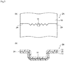
- Fig. 5 is a drawing for explaining a variant embodiment of the illumination device 1A or 1B of Fig. 1 , wherein: (a) is a diagram showing a configuration of a conductor before deformation; and (b) is a sectional view showing a configuration of a conductor after deformation.
- an illumination device 2A is placed on the base layer 13, and is provided with conductors 24 and 24 to be connected to the light source 11 to supply power to the light source 11.
- the conductors 24 and 24 are sandwiched between the reflective layer 12 and the base layer 13 to extend along a widthwise direction of the base layer 13 having a rectangular shape.
- One of the conductors 24 and 24 extends from the light source 11 to one edge portion in the widthwise direction (left-hand side) of the base layer 13 in a plan view, and the other extends from the light source 11 to the other edge portion in the widthwise direction (right-hand side) of the base layer 13.
- the conductors 24 and 24 have a zigzag shape on the base layer 13. By this zigzag shape, when the reflective layer 12 and the base layer 13 deforms three-dimensionally, the conductors 24 and 24 follow the deformation of the reflective layer 12 and the base layer 13 and deform three-dimensionally ( Fig. 5 (b) ). Thus, the conductors 24 and 24 can easily deform along with the deformation of the reflective layer 12 and the base layer 13, and a reliable flexibility and conduction can be ensured in the illumination device 2B after deformation.
- the conductors 24 and 24 have a zigzag shape, but it is not limited thereto, and may have a meander shape or a labyrinth shape.
- the meander shape or the labyrinth shape can be formed into a shape similar to the wire rod by providing notches in alternation at both ends in the widthwise direction of the conductor 24 before placing the reflective layer 12 on the base layer 13. Since the conductors 24 and 24 have a meander shape or a labyrinth shape, a further reliable flexibility and conduction can be ensured.
- Fig. 6 is a sectional view indicating a variant embodiment of the conductor 24 in the illumination device 2A or 2B of Fig. 5 , wherein: (a) is a diagram showing a state before deformation; and (b) is a diagram showing a state after the deformation. Since the illumination device of Fig. 6 is basically the same as the illumination device of Fig. 5 , overlapping description is omitted and different parts will be described below.
- an illumination device 3A is placed on the base layer 13, and is provided with conductors 34 and 34 to be connected to the light source 11 to supply power to the light source 11.
- the conductor 34 has a first conductor 34a placed on the surface 13a of the base layer 13 and a second conductor 34b placed on a side of the first conductor 34a opposite to the base layer 13.
- the conductor 34 has a slide portion 35 at a position where the first conductor 34a and the second conductor 34b are placed on top of each other, and the second conductor 34b is slidably attached along a longitudinal direction of the first conductor 34a and on the first conductor 34a.
- the second conductor 34b slides on the first conductor 34a at the slide portion 35, and along with the deformation of the reflective layer 12 and the base layer 13, the conductors 34 and 34 deform three-dimensionally ( Fig. 6 (b) ).
- the movement of the second conductor 34b in the widthwise direction is restricted by a joint between the reflective layer 12 and the base layer 13, and the second conductor 34b slides while maintaining a surface contact with the first conductor 34a.
- the conductors 34 and 34 can be easily deformed along with the deformation of the reflective layer 12 and the base layer 13, and a reliable flexibility and conduction can be obtained for the illumination device 3B after the deformation.
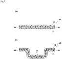
- Fig. 7 is a sectional view indicating another variant embodiment of the conductor in the illumination device 2A and 2B of Fig. 5 , wherein: (a) is a diagram showing a state before deformation; and (b) is a diagram showing a state after the deformation. Since the illumination device of Fig. 7 is also basically the same as the illumination device of Fig. 5 , overlapping description is omitted and different parts will be described below.
- an illumination device 4A is placed on the base layer 13, and is provided with conductors 44 and 44 to be connected to the light source 11 to supply power to the light source 11.
- the conductors 44 and 44 are made of an electrically conductive resin wire rod, which is, for example, a resin wire rod containing an electrically conductive filler having a spherical shape, needle shape, flake-shaped or an irregular shape.
- a wire rod having conductivity that is equivalent to a copper alloy can be selected as an electrically-conductive filler component resin rod.
- the conductors 44 and 44 deform three-dimensionally along with the deformation of the reflective layer 12 and the base layer 13 ( Fig. 7 (b) ), similarly to the case of Fig. 5 (b) .
- the resin of a base material stretches while maintaining conduction.
- the conductors 44 and 44 can be easily deformed along with the deformation of the reflective layer 12 and the base layer 13, a reliable flexibility and conduction can be obtained for the illumination device 4B after the deformation.
- the illumination device 4A or 4B can be lightweighted. Also, in a case where the light source 11 is an LED light source, light can be emitted with a low voltage, and thus a high voltage source is not required. Accordingly, by selecting a conductive resin rod having conductivity equivalent to that of metal, particularly conductivity equivalent to a copper alloy, it is possible to provide an illumination device that is more lightweight than a case where a metal conductor is used and that has conductivity equivalent to metal such as a copper alloy.
- an illumination device can be made into a laminated structure or a flattened structure by assembling electric components flatly, a special technique is not required and assembling can be facilitated. Also, by thermoforming the laminated structure or the flattened structure into a three dimensional shape, it is possible to provide an illumination device having a three-dimensional structure including a light source, a conductor, a reflective layer and a base layer. Further, the laminated structure can be formed into a flattened shape or into a roll shape, and such a laminated structure having a flattened shape can be produced in one factory.
- the final shape of the illumination device can be formed in one step in accordance with the requirement of the user. Further, since a plurality of electric components constituting an illumination device are laminated between two resins layer, the electric components can be protected from water, moisture or dust.
- the illumination device and a method of manufacturing the same according to the present embodiment are described above, but the invention is not limited to the embodiment described above, and various alterations and modifications are possible based on a technical concept of the invention.
- the conductor 14 may have a conductor compensation portion which compensates for elongation of the conductor in the longitudinal direction.
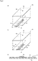
- the conductor compensation portion is a projection portion 51 which protrudes from an outer edge portion of the base layer 13, for example, as shown in Fig. 8(a) .
- the conductor compensation portion may be a bent portion 52 in which a part of the conductor 14 is bent with respect to the longitudinal direction thereof as shown in Fig. 8(b) .
- This bent portion 52 has a U-shape or a C-shape on a plan view of the base portion 13 but may have other shapes such as an S-shape.
- the conductor compensation portion may be a folded portion 53 in which a part of the conductor 14 is folded with respect to the longitudinal direction thereof as shown in Fig. 8(c) .
- This folded portion 53 constitutes an overlapping portion overlapped with respect to a thickness direction of the base layer 13, for example.
- the conductor compensation portion may have at least one recessed portion extending in a direction crossing the longitudinal direction thereof.
- the at least one recess portion is constituted by a plurality of recessed portions 54, 54, ... extending toward an inner side from both end portions of the conductor 14 in a width direction, for example, and formed along the width direction of the conductor 14 as shown in Fig. 9(a) .
- the at least one recessed portion may be constituted by a plurality of recessed portions 55, 55, ... extending toward the inner side from the both end portions of the conductor 14 in the width direction and formed with inclination to the width direction or to the longitudinal direction of the conductor 14.
- the conductor 14 can be deformed by following the deformation of the reflective layer 12 and the base layer 13 during forming, and electrical connection between the both end portions of the conductor 14 in the longitudinal direction can be maintained.
- the reflective layer 12 and the base layer 13 are formed to the desired final shapes, reliability of power supply when power is supplied to the light source 11 through the conductor 14 from outside can be improved.
- the portion of the conductor 14 corresponding to the portion in which the reflective layer 12 and the base layer 13 together undergo shape deformation during the forming of the final shape of the illumination device that is, the intermediate portion 14a of the conductor 14 in the longitudinal direction, for example, is not joined to the base layer 13, and the other portion of the conductor 14 corresponding to the portion in which neither of the reflective layer 12 nor the base layer 13 undergoes shape deformation, that is, one end portion 14b of the conductor 14 in the longitudinal direction, for example, may be joined to the base layer 13.
- the one end portion 14b of the conductor 14 is joined to the base layer 13, and in a region other than that, the conductor 14 does not have to be joined to the base layer 13.
- the other portion of the conductor 14 corresponding to the portion in which none of the reflective layer 12 and the base layer 13 undergoes shape deformation may be joined to the base layer 13.
- the other end portion 14c of the conductor 14 in the longitudinal direction may be joined to the base layer 13.
Landscapes
- Engineering & Computer Science (AREA)
- General Engineering & Computer Science (AREA)
- Microelectronics & Electronic Packaging (AREA)
- Arrangement Of Elements, Cooling, Sealing, Or The Like Of Lighting Devices (AREA)
- Non-Portable Lighting Devices Or Systems Thereof (AREA)
- Non-Metallic Protective Coatings For Printed Circuits (AREA)
- Structure Of Printed Boards (AREA)
- Led Device Packages (AREA)
- Fastening Of Light Sources Or Lamp Holders (AREA)
- Planar Illumination Modules (AREA)
Abstract
Description
- The invention relates an illumination device that reflects light emitted from a light source and a manufacturing method thereof, and particularly relates to an illumination device comprising a laminated structure obtained by laminating a thermoformable sheet substrate and a reflective sheet and a method of manufacturing the same.
- As an example of conventional illumination devices, an illumination sign assembly has been disclosed which comprises a reflective housing made of a thermoformed resin having a linear semicircular inner surface lined by highly reflective resin sheet and a clear resin sheet having a smaller dimension of cut off opening area whereby a sign face is covered to pass light energy emitted from a light source enclosed in the reflective housing (Patent Document 1).
- Also, a conventional illumination device has been disclosed which comprises an LED light source, a reflector to reflect light from the LED light source and direct light outside to provide illumination, and a diffuser lens assembly comprising two lens plates. The illumination device is provided with a heatsink having a mounting surface on which a light source such as a group of LEDs can be mounted, and the light source can be mounted flat on the mounting surface to face the reflector that is assembled at the top of the housing. The reflector is designed to have various shapes to provide a particular optical function (Patent Document 2).
-
- Patent Document 1: United States Patent No.
5918396 - Patent Document 2: United States Patent Application Publication No.
2012/0262902 - However, conventional illumination devices as described above require various functional members such as a body, an LED light source, a reflector, a heatsink, and a conducting wire that need to be fabricated separately and individually. Further, it is necessary to assemble such functional members during the manufacture, and thus the manufacturing process becomes complicated and operations thereof become cumbersome.
- If the manufacturing process of the illumination device can be simplified, production costs can be reduced and productivity can be improved. However, the conventional illumination devices described above require design costs and production costs for each of the functional members and further requires assembly costs, thus resulting in an increased production costs for the illumination devices. Particularly, since electric members, mechanical members and optical members of the conventional illumination devices are generally fabricated by different manufacturers at different locations, transportation costs for each member incidentally occur. Also, since the plurality of members of the conventional illumination devices are designed and produced different manufacturers, a multi-stage assembly technique is eventually required.
- It is an object of the invention to provide an illumination device having a simple structure that can be assembled in a facilitated manner and with reduced costs, and a method of manufacturing such an illumination device.
- In order to achieve the above mentioned object, an illumination device according to invention is characterized by comprising at least one light source, a reflective layer disposed to reflect light from the at least one light source and to direct the light out of the illumination device to provide illumination, a base layer of a thermoformed resin to hold the at least one light source and to hold the reflective layer, and a plurality of conductors disposed on the base layer and connected to the at least one light source to supply power to the at least one light source.
- It is preferable that the at least one light source includes at least one LED light source.
- It is preferable that the reflective layer is made of a thermoformable resin.
- It is preferable that the reflective layer is made of foamed polyethylene terephthalate.
- It is preferable that the reflective layer has a thickness of 0.01 mm to 5 mm, and further preferably, 0.5 mm to 1 mm.
- The base layer is disposed to assemble the at least one light source and the plurality of conductors thereon.
- It is preferable that the base layer is a printed circuit board.
- It is preferable that the base layer has a thickness of 0.1 mm to 10 mm, and more preferably, 1 mm to 2 mm.
- It is preferable that the conductor has a conductor compensation portion which compensates for elongation of the conductor in a longitudinal direction.
- The conductor compensation portion may be a projection portion protruding from an outer edge portion of the base layer.
- The conductor compensation portion may be a bent portion in which a part of the conductor is bent with respect to the longitudinal direction thereof.
- The conductor compensation portion may have at least one recessed portion extending in a direction crossing the longitudinal direction.
- A portion of the conductor corresponding to a portion in which the reflective layer and the base layer together undergo shape deformation during forming is not joined to the base layer, and the other portion of the conductor corresponding to a portion in which neither of the reflective layer nor the base layer undergoes shape deformation may be joined to the base layer.
- It is preferable that the plurality of conductors are made of one of sheet metal, metal pad, metal foil, wire rod and patterned conductor, and more preferably, patterned conductors on a printed circuit board.
- The illumination device further comprises at least one through-hole portion provided in the reflective layer to emit light from the at least one light source to outside.
- Further, the reflective layer and the base layer have an identical shape.
- The reflective layer is assembled onto the base layer with a plurality of conductors being located between the reflective layer and the base layer.
- The at least one light source is a single LED light source assembled onto a surface of the base layer, and the at least one through-hole has a single through-hole portion positioned at a position corresponding to the single LED light source so that light from the single LED light source either leaves directly the illumination device through the single through-hole portion or is reflected back from the surface of the opposite side of the reflective layer which is not connected to the base layer.
- The plurality of conductors have a terminal portion for connecting a power supply to the single LED light source.
- In order to achieve the above mentioned object, a method of manufacturing an illumination device is characterized by including preparing a reflective layer as a thermoformable resin sheet, preparing a base layer as a thermoformed resin sheet, providing a plurality of conductors on a surface of the base layer, providing a terminal portion of the plurality of conductors to supply power to at least one light source, providing the at least one light source whereto the plurality of conductors are connected on a surface of the base layer, providing at least one through-hole portion in the reflective layer, placing the reflective layer on the base layer so that the plurality of conductors are positioned between the reflective layer and the base layer, and positioning the reflective layer on the base layer so that light from the at least one light source either leaves directly the illumination device through the at least one through-hole portion or is reflected back from a surface on an opposite side of the reflective layer that is not connected to the base layer, and the at least one through-hole portion of the reflective layer is positioned at a position corresponding to the at least one light source assembled to a surface of the base layer.
- The plurality of conductors are made flexible in order not to break when the base layer undergoes shape deformation.
- The terminal portion is assembled to an edge portion of a shape after deformation of the base layer or opposite side of the base layer that is not joined to the reflective layer.
- The reflective layer and the base layer are joined to each other by polymer melting.
- The polymer melting is lamination.
- The reflective layer and the base layer are polymer softened by heat using a mold having a shape that is identical to a final shape of the illumination device so that the reflective layer and the base layer together undergo shape deformation into the final shape of the illumination device.
- The polymer softening is thermoformation.
- The final shape of the illumination device is obtained by cutting the reflective layer and the base layer.
- In providing the plurality of conductors on a surface of the base layer, a portion of the conductor corresponding to a portion in which the reflective layer and the base layer together undergo shape deformation during forming in order to obtain the final shape of the illumination device does not have to be joined to the base layer, and the other portion of the conductor corresponding to the portion in which neither of the reflective layer nor the base layer undergoes shape deformation may be joined to the base layer.
- According to the invention, it is possible to provide an illumination device having a simple structure that can be assembled in a facilitated manner and with reduced costs, and a method of manufacturing such an illumination device.
-
- [
Fig. 1] Fig. 1 is a drawing schematically showing an illumination device according to an embodiment of the invention, wherein: (a) is a perspective view; (b) is an exploded perspective view; and (c) is a sectional view taken along line I-I in (a). - [
Fig. 2] Fig. 2 is a drawing showing a state after deformation of the illumination device ofFig. 1 , wherein: (a) is a plan view; (b) is a bottom plan view; and (c) is a sectional view taken along line II-II in (a). - [
Fig. 3] Fig. 3 is a plan view showing a state where power is supplied to the illumination device ofFig. 2 . - [
Fig. 4] Fig. 4 is a drawing in which (a) to (g) are sectional views illustrating each step of a method of manufacturing the illumination device ofFig. 1 . - [
Fig. 5] Fig. 5 is a drawing for explaining a variant embodiment of the illumination device ofFig. 1 , wherein: (a) is a diagram showing a configuration of a conductor before deformation; and (b) is a sectional view showing a configuration of a conductor after deformation. - [
Fig. 6] Fig. 6 is a sectional view indicating a variant embodiment of the conductor in the illumination device ofFig. 5 , wherein: (a) is a diagram showing a state before deformation; and (b) is a diagram showing a state after deformation. - [
Fig. 7] Fig. 7 is a sectional view indicating another variant embodiment of the conductor in the illumination device ofFig. 5 , wherein: (a) is a diagram showing a state before deformation; and (b) is a diagram showing a state after deformation. - [
Fig. 8] Fig. 8 is drawing in which (a) is an exploded perspective view showing a conductor compensation portion provided on the conductor; (b) is an exploded perspective view showing a variant of the conductor compensation portion; and (c) is a longitudinal sectional view showing a variant of the conductor compensation portion. - [
Fig. 9] Fig. 9 is a drawing in which (a) is a partial perspective view showing a variant of the conductor compensation portion; and (b) is a partial perspective view showing a variant of the conductor compensation portion. - [
Fig. 10] Fig. 10 is a partially exploded perspective view showing a variant of the illumination device inFig. 1 . - Hereinafter, preferred embodiments of the invention will be described in detail with reference to the attached drawings.
-
Fig. 1 is a drawing schematically showing an illumination device (also referred to as a luminaire) according to an embodiment of the invention, wherein: (a) is a perspective view; (b) is an exploded perspective view; and (c) is a sectional view taken along line I-I in (a). The illumination device ofFig. 1 is shown by way of example, and the configuration of the illumination device according to the invention is not limited the configuration shown inFig. 1 . - A shown in
Fig. 1(a) to (c) , anillumination device 1A includes alight source 11, areflective layer 12 that is disposed to reflect light from thelight source 11 and to direct the light out of theillumination device 1A to provide illumination, abase layer 13 made of a thermoformed resin (also referred to as a thermoplastic) for holding thelight source 11 and for holding thereflective layer 12,conductors base layer 13 and connected to thelight source 11 to supply power to thelight source 11, and a through-hole portion 15 provided in thereflective layer 12 to emit light from thelight source 11 to outside. - The
light source 11 is, for example, an LED light source. In the present embodiment, theillumination device 1A is provided with a singlelight source 11, but, it is not limited thereto, and at least one light source may be provided depending on design. In this case, the at least one light source described above may include at least one LED light source. - The
reflective layer 12 is an optical reflective part having a planar geometry, such as a thin plate, a sheet or a thin layer, and is made of a thermoformable resin (also referred to as a thermoformable plastic), such as a thermoplastic resin. Preferably, thereflective layer 12 is made of foamed PET (polyethylene terephthalate) such as MCPET (registered trademark). Thereflective layer 12 is highly reflective, and reflects light from thelight source 11 at a high reflectance. - In a case where the reflective layer has a transmittance of 1 to 5%, optical efficiency of the illumination device is affected. Thus by combining the
reflective layer 12 with thebase layer 13 made of a thermoformed resin having an extremely small transmittance, particularly made of a thermoplastic resin having an extremely small transmittance, optical reflectance of theillumination device 1A can be maximized, and optical efficiency can be improved. - In a case where the
reflective layer 12 is MCPET, total reflectance is greater than or equal to 99% and diffuse reflectance is greater than or equal to 96% taken as relative values with respect a barium sulfate white board of 550 nm. Also, MCPET has a transmittance of approximately 1.5% with a thickness of 0.5 mm to 1 mm. Further, MCPET is has a high stiffness, and can be subjected to secondary processing such as bending or molding. Further, although a reflection member made of normal plastics cannot meet a required level, PCPET has flame retardancy and thus can meet a required flammability level. - The
reflective layer 12 has the through-hole portion 15 penetrating therethrough in a thickness direction thereof. The through-hole portion 15 is positioned at a position corresponding to thelight source 11 assembled to a surface of thebase layer 13 and the geometry (shape and measure) of the through-hole portion 15 is substantially or essentially identical with that of thelight source 11 assembled onto the surface of thebase layer 13. Thereby, light from thelight source 11 either leaves directly theillumination device 1A through the through-hole portion 15 or is reflected back from the surface of the opposite side of thereflective layer 12 which is not connected to thebase layer 13. In the present embodiment, theillumination device 1A is provided with one through-hole portion 15, but it is not limited thereto, and at least one through-hole portion may be provided depending on design. - The
base layer 13 is a base part placed to assemble thelight source 11 and the plurality ofconductors base layer 13 can be disposed as a PCB (printed circuit board) to assemble all electronic components including, in addition to thelight source 11 and the plurality ofconductors base layer 13 has all electric components assembled to thebase layer 13, and thus plays two roles, which is to provide a function as theillumination device 1A, as well as a function of providing mechanical characteristics of the structure of theillumination device 1A such as stiffness, flame retardancy, non-shrinkage, electric insulation, and thermal conduction. - It is preferable that the
reflective layer 12 and thebase layer 13 are joined with each other by polymer melting. This polymer melting is the laminating which, for example, adheres thereflective layer 12 and thebase layer 13 with each other. Also, it is preferable that thereflective layer 12 and thebase layer 13 have an identical shape. - The thickness of the
reflective layer 12 is preferably 0.01 mm to 5 mm, and more preferably, 0.5 mm to 1 mm. The thickness of thebase layer 13 is preferably 0.1 mm to 10 mm and more preferably 1 mm to 2 mm. - The
conductors reflective layer 12 and thebase layer 13 to extend along a longitudinal direction of thebase layer 13 having a rectangular shape, and are disposed in a parallel so as not to come into contact with each other. Theconductors base layer 13 is deformed. Theconductors light source 11 on thebase layer 13 and other optical and electrical characteristics (e.g., color and light intensity of the LED light source) can be changed or adjusted with the arrangement of theconductors 14 and 14 (e.g., patterned conductors on the PCB) and the arrangement of other electric components. Theconductors conductors conductors light source 11. - The
conductors base layer 13. For example, theconductor 14 is fixed to thebase layer 13 by thermal lamination such as pressing, adhesion using an adhesive, ultrasonic welding, thermal welding, or laser welding. - The
conductors terminal portions light source 11. Theterminal portions conductors Fig. 2 ) of a shape after deformation of thebase layer 13 or opposite side of the base layer that is not connected to thereflective layer 12. Theseterminal portions conductors conductors -
Fig. 2 is a drawing showing a state after deformation of the illumination device ofFig. 1 , wherein: (a) is a plan view; (b) is a bottom plan view; and (c) is a sectional view taken along line II-II in (a). - As shown in
Fig. 2 (a) to (c) , theillumination device 1B has a laminated structure including thereflective layer 12 and thebase layer 13 that are laminated, and the laminated structure has aflat portion 1B-1 and a recessedportion 1B-2. The recessedportion 1B-2 is formed integrally with theflat portion 1B-1 by thermoforming. In other words, theillumination device 1B has a protruded portion corresponding to the recessedportion 1B-2, the protruded portion that is protruded from thereflective layer 12 side to thesupport 13 side in a thickness direction of theflat portion 1B-1. Accordingly, theillumination device 1B ofFig. 2 is the basically same as theillumination device 1A ofFig. 1 , except the recessedportion 1B-2. It is preferable that thereflective layer 12 and thebase layer 13 are of the same geometry. - The
flat portion 1B-1 has a sheet shape or a thin plate shape, and has a substantially rectangular shape in a plan view. The geometry of theflat portion 1B-1 in a plan view can be made into other shapes such as a circle, an ellipse or a polygon depending on design. Theflat portion 1B-1 has a thickness of 1 mm to 5 mm. - The recessed
portion 1B-2 is a three-dimensionally molded dome-shaped portion, and has an annular shape or a substantially annular shape in a sectional view in a direction of the plane. The recessedportion 1B-2 a trapezoid or a generally trapezoid shape in a sectional view in a thickness direction. Like theflat portion 1B-1, the recessedportion 1B-2 has a thickness of 1 mm to 5 mm. - The sectional shape in the direction of the plane and the sectional shape in the direction of the thickness of the recessed
portion 1B-2 may be other shapes such as a circle, an ellipse or a polygon depending on design. Further, in the present embodiment, the recessedportion 1B-2 is formed to have a continuous surface, but it may be formed to have a discontinuous surface with one or a plurality of through-hole portions or a mesh structure. - The recessed
portion 1B-2 has abase wall 1B-3 and aside wall 1B-4, and thebase wall 1B-3 and theside wall 1B-4 are formed integrally. In the present embodiment, thelight source 11 is placed at a substantially central part in a plan view of thebase wall 1B-3 (Fig. 2 (a) ). Theconductors light source 11 to theedge portion 1B-5 of theflat portion 1B-1 via thebase wall 1B-3 and theside wall 1B-4 and are connected to theterminal portion edge portion 1B-5. -
Fig. 3 is a plan view showing a state where power is supplied to theillumination device 1B ofFig. 2 .Terminals terminal portions light source 11, and light is emitted from thelight source 11. - The light emitted from the
light source 11 is roughly categorized into direct light and reflected light, and the reflected light varies depending on the geometry of thebase wall 1B-3 and theside wall 1B-4 of the recessedportion 1B-2. Accordingly, a light emitting position when theillumination device 1B is viewed from thereflective layer 12 side can be changed by changing the shape, the dimension or the like of the recessedportion 1B-2 depending on design. In this embodiment, when the user sees theillumination device 1B from thereflective layer 12 side, both the direct light emitted from thelight source 11 and the reflected light that has reflected off theside wall 1B-4 reach the user. Thereby, a circular light emitting part corresponding to thelight source 11 and a ring-shaped light emitting part surrounding the light emitting part and corresponding toside wall 1B-4 are viewed. - A method of manufacturing the
illumination device Fig. 2 will be described with reference toFig. 4 . - First, the
reflective layer 12 as a thermoformable resin sheet is prepared, and further, thebase layer 13 as a thermoformed resin sheet is prepared (Fig. 4(a) ). Also, amold 20 having a shape which is the same as a shape (final shape) of theillumination device 1B to be obtained at a final stage is prepared (seeFig. 4(f) ). For example, the mold is a metal mold for plastics which is a metal mold having an elongated geometry with an end portion in the longitudinal direction being R-chamfered. - Thereafter, the
conductors surface 13a of the base layer 13 (Fig. 4 (b) ), and further, theterminal portions conductors light source 11. Theterminal portions edge portion 1B-5 of a shape after deformation of thebase layer 13 to be described below and/or assembled to asurface 13b on an opposite side of thebase layer 13 that is not joined to thereflective layer 12. Theconductors terminal portions conductors surface 13a of thebase layer 13, theterminal portions surface 13b on an opposite side of thebase layer 13 or on a side surface of thebase layer 13 by bending end portions of theconductors - Moreover, in this process in which the
conductors 14 are provided on thesurface 13a of thebase layer 13, it is preferable that a portion of theconductor 14 corresponding to a portion in which thereflective layer 12 and thebase layer 13 together undergo shape deformation during forming in order to obtain the final shape of theillumination device 1B, that is, an intermediate portion of theconductor 14 in a longitudinal direction, for example, is not joined to thebase layer 13, and the other portion of theconductor 14 corresponding to a portion in which neither of thereflective layer 12 nor thebase layer 13 undergoes shape deformation, that is, both end portions of theconductor 14 in the longitudinal direction, for example, is joined to the base layer (seeFig. 10 ). - Then, the
conductors light source 11 is connected are provided on thesurface 13a of the base layer 13 (Fig. 4 (c) ). Thelight source 11 is attached at an end portion of theconductor conductors conductors - Thereafter, a through-
hole portion 15 is provided in the reflective layer 12 (Fig. 4 (d) ), and then thereflective layer 12 is placed on thebase layer 13 such that theconductor reflective layer 12 and the base layer 13 (Fig. 4 (e) ). Here, the position of the through-hole portion 15 is accurately placed directly above the position of thelight source 11 and the shape of through-hole portion 15 is identical to the shape of thelight source 11. - Then, the
reflective layer 12 is positioned above thebase layer 13 such that light from thelight source 11 either leaves directly theillumination device 1A through the through-hole portion 15 or is reflected back from thesurface 12a of the opposite side of thereflective layer 12 which is not connected to thebase layer 13, and also such that the through-hole portion 15 of thereflective layer 12 is positioned at a position corresponding to thelight source 11 assembled onto thesurface 13a of the base layer 13 (Fig. 4 (e) ). - Then, with the
conductors reflective layer 12 and thebase layer 13, thereflective layer 12 and thebase layer 13 are joined by thermoforming. Thereflective layer 12 and thebase layer 13 are preferably joined by polymer melting, but may be joined to each other via another member such as an adhesive material. - Subsequently, the
reflective layer 12 and thebase layer 13 are polymer softened by heat using amold 20 having a shape which is the same as the final shape of theillumination device 1B so that thereflective layer 12 and thebase layer 13 together undergo shape deformation into the final shape of theillumination device 1B (Fig. 4 (f) ). Such polymer softening is thermoforming, and polymer softening is performed by pressing the mold heated to a predetermined temperature against thesurface 12a of thereflective layer 12. For example, the mold is a metal mold, and formed using one or a plurality of metal molds. The mold has a rod-shape, but it may have other shapes such as a shape of a hat, a shape of a flower, or a shape of a bottle. Note that although the polymer melting and the polymer softening may be performed by different processes, they are preferably performed by a single step for simplification of the manufacturing process. - During this, the
conductor reflective layer 12 and thebase layer 13 do not break because of their flexibility, and thus sufficient conduction is ensured between thelight source 11 and theterminal portions conductors reflective layer 12 and thebase layer 13. - Subsequently, the edge portion in a direction of plane of the integrated
reflective layer 12 and thebase layer 13 is cut depending on design, and the final shape of theillumination device 1B having theflat portion 1B-1 and the recessedportion 1B-2 (Fig. 4 (g) ) is obtained. - As described above, the
illumination device 1A includes alight source 11, areflective layer 12 disposed to reflect light from thelight source 11 and to direct the light out of theillumination device 1A to provide illumination, abase layer 13 made of thermoformed resin to hold thelight source 11 and to hold thereflective layer 12, and a plurality ofconductors base layer 13 and connected to thelight source 11 to supply power to thelight source 11. Accordingly, theillumination device 1A can be obtained by simply integrating thelight source 11, thereflective layer 12, thebase layer 13, theconductors terminal portions illumination device 1B can be manufactured by designing the mold and integrating thelight source 11, theconductors terminal portions base layer 13, and thereafter joining thereflective layer 12 and thebase layer 13 with each other using the aforementioned mold and also heat deforming them. Thus, a manufacturing process of theillumination device 1B can be simplified into a single main step, which is thermoforming. - Also, the
illumination device 1B manufactured as described above is capable of immediately emitting light from thelight source 11 by simply supplying power to theterminal portions illumination device 1B can cut theflat portion 1B-1 into a desired shape except for a portion where theconductors - Further, based on a particular design of the
illumination device 1A, thelight source 11, theconductors base layer 13 as elements of a circuit board. Thereby, (i)illumination devices base layer 13 and thereflective layer 12 by thermoforming thebase layer 13 and thereflective layer 12 on a top face thereof. Thereby, electric, humidity and moisture insulating properties can be ensured, and theillumination device -
Fig. 5 is a drawing for explaining a variant embodiment of theillumination device Fig. 1 , wherein: (a) is a diagram showing a configuration of a conductor before deformation; and (b) is a sectional view showing a configuration of a conductor after deformation. - As shown in
Fig. 5 (a) , anillumination device 2A is placed on thebase layer 13, and is provided withconductors light source 11 to supply power to thelight source 11. Theconductors reflective layer 12 and thebase layer 13 to extend along a widthwise direction of thebase layer 13 having a rectangular shape. One of theconductors light source 11 to one edge portion in the widthwise direction (left-hand side) of thebase layer 13 in a plan view, and the other extends from thelight source 11 to the other edge portion in the widthwise direction (right-hand side) of thebase layer 13. - The
conductors base layer 13. By this zigzag shape, when thereflective layer 12 and thebase layer 13 deforms three-dimensionally, theconductors reflective layer 12 and thebase layer 13 and deform three-dimensionally (Fig. 5 (b) ). Thus, theconductors reflective layer 12 and thebase layer 13, and a reliable flexibility and conduction can be ensured in theillumination device 2B after deformation. - The
conductors conductor 24 before placing thereflective layer 12 on thebase layer 13. Since theconductors -
Fig. 6 is a sectional view indicating a variant embodiment of theconductor 24 in theillumination device Fig. 5 , wherein: (a) is a diagram showing a state before deformation; and (b) is a diagram showing a state after the deformation. Since the illumination device ofFig. 6 is basically the same as the illumination device ofFig. 5 , overlapping description is omitted and different parts will be described below. - As shown in
Fig. 6 , anillumination device 3A is placed on thebase layer 13, and is provided withconductors light source 11 to supply power to thelight source 11. Theconductor 34 has afirst conductor 34a placed on thesurface 13a of thebase layer 13 and asecond conductor 34b placed on a side of thefirst conductor 34a opposite to thebase layer 13. Theconductor 34 has aslide portion 35 at a position where thefirst conductor 34a and thesecond conductor 34b are placed on top of each other, and thesecond conductor 34b is slidably attached along a longitudinal direction of thefirst conductor 34a and on thefirst conductor 34a. - When the
reflective layer 12 and thebase layer 13 are deformed three-dimensionally, thesecond conductor 34b slides on thefirst conductor 34a at theslide portion 35, and along with the deformation of thereflective layer 12 and thebase layer 13, theconductors Fig. 6 (b) ). The movement of thesecond conductor 34b in the widthwise direction is restricted by a joint between thereflective layer 12 and thebase layer 13, and thesecond conductor 34b slides while maintaining a surface contact with thefirst conductor 34a. Thus, theconductors reflective layer 12 and thebase layer 13, and a reliable flexibility and conduction can be obtained for theillumination device 3B after the deformation. -
Fig. 7 is a sectional view indicating another variant embodiment of the conductor in theillumination device Fig. 5 , wherein: (a) is a diagram showing a state before deformation; and (b) is a diagram showing a state after the deformation. Since the illumination device ofFig. 7 is also basically the same as the illumination device ofFig. 5 , overlapping description is omitted and different parts will be described below. - As shown in
Fig. 7 , anillumination device 4A is placed on thebase layer 13, and is provided withconductors light source 11 to supply power to thelight source 11. Theconductors - When the
reflective layer 12 and thebase layer 13 are deformed three-dimensionally, theconductors reflective layer 12 and the base layer 13 (Fig. 7 (b) ), similarly to the case ofFig. 5 (b) . Here, in theconductors conductors reflective layer 12 and thebase layer 13, a reliable flexibility and conduction can be obtained for theillumination device 4B after the deformation. - Also, since the mass of the conductive resin rod is smaller than that of metal, the
illumination device light source 11 is an LED light source, light can be emitted with a low voltage, and thus a high voltage source is not required. Accordingly, by selecting a conductive resin rod having conductivity equivalent to that of metal, particularly conductivity equivalent to a copper alloy, it is possible to provide an illumination device that is more lightweight than a case where a metal conductor is used and that has conductivity equivalent to metal such as a copper alloy. - According to the invention, an illumination device can be made into a laminated structure or a flattened structure by assembling electric components flatly, a special technique is not required and assembling can be facilitated. Also, by thermoforming the laminated structure or the flattened structure into a three dimensional shape, it is possible to provide an illumination device having a three-dimensional structure including a light source, a conductor, a reflective layer and a base layer. Further, the laminated structure can be formed into a flattened shape or into a roll shape, and such a laminated structure having a flattened shape can be produced in one factory.
- Also, the final shape of the illumination device can be formed in one step in accordance with the requirement of the user. Further, since a plurality of electric components constituting an illumination device are laminated between two resins layer, the electric components can be protected from water, moisture or dust.
- The illumination device and a method of manufacturing the same according to the present embodiment are described above, but the invention is not limited to the embodiment described above, and various alterations and modifications are possible based on a technical concept of the invention.
- For example, the
conductor 14 may have a conductor compensation portion which compensates for elongation of the conductor in the longitudinal direction. The conductor compensation portion is aprojection portion 51 which protrudes from an outer edge portion of thebase layer 13, for example, as shown inFig. 8(a) . - Moreover, the conductor compensation portion may be a
bent portion 52 in which a part of theconductor 14 is bent with respect to the longitudinal direction thereof as shown inFig. 8(b) . Thisbent portion 52 has a U-shape or a C-shape on a plan view of thebase portion 13 but may have other shapes such as an S-shape. - The conductor compensation portion may be a folded
portion 53 in which a part of theconductor 14 is folded with respect to the longitudinal direction thereof as shown inFig. 8(c) . This foldedportion 53 constitutes an overlapping portion overlapped with respect to a thickness direction of thebase layer 13, for example. - Moreover, the conductor compensation portion may have at least one recessed portion extending in a direction crossing the longitudinal direction thereof. The at least one recess portion is constituted by a plurality of recessed
portions conductor 14 in a width direction, for example, and formed along the width direction of theconductor 14 as shown inFig. 9(a) . Moreover, as shown inFig. 9(b) , the at least one recessed portion may be constituted by a plurality of recessedportions conductor 14 in the width direction and formed with inclination to the width direction or to the longitudinal direction of theconductor 14. - As described above, by providing the conductor compensation portion on the
conductor 14, theconductor 14 can be deformed by following the deformation of thereflective layer 12 and thebase layer 13 during forming, and electrical connection between the both end portions of theconductor 14 in the longitudinal direction can be maintained. Thus, in a state where thereflective layer 12 and thebase layer 13 are formed to the desired final shapes, reliability of power supply when power is supplied to thelight source 11 through theconductor 14 from outside can be improved. - Moreover, as shown in
Fig. 10 , the portion of theconductor 14 corresponding to the portion in which thereflective layer 12 and thebase layer 13 together undergo shape deformation during the forming of the final shape of the illumination device, that is, theintermediate portion 14a of theconductor 14 in the longitudinal direction, for example, is not joined to thebase layer 13, and the other portion of theconductor 14 corresponding to the portion in which neither of thereflective layer 12 nor thebase layer 13 undergoes shape deformation, that is, oneend portion 14b of theconductor 14 in the longitudinal direction, for example, may be joined to thebase layer 13. In other words, in a light-source neighboring region 61 which is neighboring to thelight source 11, the oneend portion 14b of theconductor 14 is joined to thebase layer 13, and in a region other than that, theconductor 14 does not have to be joined to thebase layer 13. - As a result, while adhesion of the
conductor 14 on thebase layer 13 is simplified, insulating reliability of theconductors conductor 14 can be deformed easily by following the deformation of thereflective layer 12 or thebase layer 13 during forming, and reliability of power supply to thelight source 11 after the forming can be improved. - Moreover, the other portion of the
conductor 14 corresponding to the portion in which none of thereflective layer 12 and thebase layer 13 undergoes shape deformation, that is, theother end portion 14c of theconductor 14 in the longitudinal direction, for example, may be joined to thebase layer 13. In other words, it is preferable that, in an outer-edge neighboring region 62 including the outer edge portion of thebase layer 13, theother end portion 14c of theconductor 14 is joined to thebase layer 13. As a result, while reliability of power supply to thelight source 11 after forming is improved, insulating reliability of theconductors -
- 1A
- illumination device
- 1B
- illumination device
- 2A
- illumination device
- 2B
- illumination device
- 3A
- illumination device
- 3B
- illumination device
- 4A
- illumination device
- 4B
- illumination device
- 11
- light source
- 12
- reflective layer
- 12a
- surface
- 13
- base layer
- 13a
- surface
- 13b
- surface
- 14
- conductor
- 15
- through-hole portion
- 16
- terminal portion
- 17
- terminal
- 1B-1
- flat portion
- 1B-2
- recessed portion
- 1B-3
- base wall
- 1B-4
- side wall
- 1B-5
- edge portion
- 20
- mold
- 24
- conductor
- 34
- conductor
- 34a
- first conductor
- 34b
- second conductor
- 35
- slide portion
- 44
- conductor
Claims (31)
- An illumination device comprising:at least one light source;a reflective layer disposed to reflect light from the at least one light source and to direct the light out of the illumination device to provide illumination;a base layer of a thermoformed resin to hold the at least one light source and to hold the reflective layer; anda plurality of conductors disposed on the base layer and connected to the at least one light source to supply power to the at least one light source.
- The illumination device according to claim 1, wherein the at least one light source includes at least one LED light source.
- The illumination device according to claim 1, wherein the reflective layer is made of a thermoformable resin.
- The illumination device according to claim 3, wherein the reflective layer is made of foamed polyethylene terephthalate.
- The illumination device according to claim 3, wherein the reflective layer has a thickness of 0.01 mm to 5 mm.
- The illumination device according to claim 5, wherein the reflective layer has a thickness of 0.5 mm to 1 mm.
- The illumination device according to claim 1, wherein the base layer is disposed to assemble the at least one light source and the plurality of conductors thereon.
- The illumination device according to claim 7, wherein the base layer is a printed circuit board.
- The illumination device according to claim 7, wherein the base layer has a thickness of 0.1 mm to 10 mm.
- The illumination device according to claim 9, wherein the base layer has a thickness of 1 mm to 2 mm.
- The illumination device according to claim 1, wherein the conductor has a conductor compensation portion which compensates for elongation of the conductor in a longitudinal direction.
- The illumination device according to claim 11, wherein the conductor compensation portion is a projection portion which protrudes from an outer edge portion of the base layer.
- The illumination device according to claim 11, wherein the conductor compensation portion is a bent portion in which a part of the conductor is bent with respect to the longitudinal direction thereof.
- The illumination device according to claim 11, wherein the conductor compensation portion has at least one recessed portion extending in a direction crossing the longitudinal direction thereof.
- The illumination device according to claim 1, wherein a portion of the conductor corresponding to a portion in which the reflective layer and the base layer together undergo shape deformation during forming is not joined to the base layer, and the other portion of the conductor corresponding to a portion in which neither of the reflective layer nor the base layer undergoes shape deformation is joined to the base layer.
- The illumination device according to claim 1, wherein the plurality of conductors are any one of metal sheets, metal pads, metal foils, wire rods, and pattern conductors.
- The illumination device according to claim 16, wherein the plurality of conductors are pattern conductors on a printed circuit board.
- The illumination device according to claim 1, further comprising at least one through-hole portion provided in the reflective layer to emit light from the at least one light source to outside.
- The illumination device according to claim 18, wherein the reflective layer and the base layer have an identical shape.
- The illumination device according to claim 19, wherein the reflective layer is assembled onto the base layer with a plurality of conductors being located between the reflective layer and the base layer.
- The illumination device according to claim 20, wherein the at least one light source is a single LED light source assembled onto a surface of the base layer, the at least one through-hole is a single through-hole positioned at a position corresponding to the single LED light source so that light from the single LED light source either leaves directly the illumination device through the single through-hole portion or is reflected back from the surface of the opposite side of the reflective layer which is not connected to the base layer.
- The illumination device according to claim 21, wherein the plurality of conductors have a terminal portion for connecting a power supply to the single LED light source.
- A method of manufacturing an illumination device, the method comprising:preparing a reflective layer as a thermoformable resin sheet;preparing a base layer as a thermoformed resin sheet;providing a plurality of conductors on a surface of the base layer;providing a terminal portion of the plurality of conductors to supply power to at least one light source;providing the at least one light source whereto the plurality of conductors are connected on a surface of the base layer;providing at least one through-hole portion in the reflective layer;placing the reflective layer on the base layer so that the plurality of conductors are positioned between the reflective layer and the base layer; andpositioning the reflective layer on the base layer so that light from the at least one light source either leaves directly the illumination device through the at least one through-hole portion or is reflected back from a surface on an opposite side of the reflective layer that is not connected to the base layer, and the at least one through-hole portion of the reflective layer is positioned at a position corresponding to the at least one light source assembled to a surface of the base layer.
- The method of manufacturing an illumination device according to claim 23, wherein the plurality of conductors are made flexible in order not to break when the base layer undergoes shape deformation.
- The method of manufacturing an illumination device according to claim 23, wherein the terminal portion is assembled to an edge portion of a shape after deformation of the base layer or opposite side of the base layer that is not joined to the reflective layer.
- The method of manufacturing an illumination device according to claim 25, wherein the reflective layer and the base layer are joined to each other by polymer melting.
- The method of manufacturing an illumination device according to claim 26, wherein the polymer melting is lamination.
- The method of manufacturing an illumination device according to claim 26, wherein the reflective layer and the base layer are polymer softened by heat using a mold having a shape that is identical to a final shape of the illumination device so that the reflective layer and the base layer together undergo shape deformation into the final shape of the illumination device.
- The method of manufacturing an illumination device according to claim 28, wherein the polymer softening is thermoformation.
- The method of manufacturing an illumination device according to claim 28, wherein the final shape of the illumination device is obtained by cutting the reflective layer and the base layer.
- The method of manufacturing an illumination device according to any one of claims 23 to 30, wherein in providing the plurality of conductors on the surface of the base layer, the portion of the conductor corresponding to the portion in which the reflective layer and the base layer together undergo shape deformation during forming in order to obtain the final shape of the illumination device is not joined to the base layer, and the other portion of the conductor corresponding to the portion in which neither of the reflective layer nor the base layer undergoes shape deformation is joined to the base layer.
Applications Claiming Priority (2)
| Application Number | Priority Date | Filing Date | Title |
|---|---|---|---|
| JP2017010963 | 2017-01-25 | ||
| PCT/JP2018/002280 WO2018139535A1 (en) | 2017-01-25 | 2018-01-25 | Illumination device and method for manufacturing said illumination device |
Publications (2)
| Publication Number | Publication Date |
|---|---|
| EP3576170A1 true EP3576170A1 (en) | 2019-12-04 |
| EP3576170A4 EP3576170A4 (en) | 2021-05-26 |
Family
ID=62979349
Family Applications (1)
| Application Number | Title | Priority Date | Filing Date |
|---|---|---|---|
| EP18745218.0A Withdrawn EP3576170A4 (en) | 2017-01-25 | 2018-01-25 | LIGHTING DEVICE AND METHOD FOR MANUFACTURING THE SAID LIGHTING DEVICE |
Country Status (4)
| Country | Link |
|---|---|
| US (1) | US10840422B2 (en) |
| EP (1) | EP3576170A4 (en) |
| JP (1) | JP7012413B2 (en) |
| WO (1) | WO2018139535A1 (en) |
Cited By (2)
| Publication number | Priority date | Publication date | Assignee | Title |
|---|---|---|---|---|
| TWI920905B (en) * | 2024-12-04 | 2026-04-01 | 宏碁股份有限公司 | Housing structure with light emitting design |
| US12601464B1 (en) | 2024-12-03 | 2026-04-14 | Acer Incorporated | Housing structure with light emitting design |
Family Cites Families (18)
| Publication number | Priority date | Publication date | Assignee | Title |
|---|---|---|---|---|
| US5918396A (en) | 1996-02-16 | 1999-07-06 | Jung; Hae-Ryong | Light box with edge-lit panel |
| JP4496774B2 (en) * | 2003-12-22 | 2010-07-07 | 日亜化学工業株式会社 | Manufacturing method of semiconductor device |
| JP2013058771A (en) * | 2005-10-28 | 2013-03-28 | Proteras Co Ltd | Flexible luminous body |
| EP2080947A4 (en) | 2006-10-20 | 2009-11-11 | Contents Co Ltd | Flexible luminescent material |
| US20080188020A1 (en) * | 2007-02-05 | 2008-08-07 | Kuo Wei-Min | Method of LED packaging on transparent flexible film |
| JP2009231584A (en) * | 2008-03-24 | 2009-10-08 | Japan Gore Tex Inc | Method of manufacturing led substrate and the led substrate |
| DE102011014584A1 (en) * | 2011-03-21 | 2012-09-27 | Osram Opto Semiconductors Gmbh | Connection carrier for semiconductor chips and semiconductor device |
| US9316368B2 (en) | 2011-04-18 | 2016-04-19 | Cree, Inc. | LED luminaire including a thin phosphor layer applied to a remote reflector |
| JP2013093379A (en) * | 2011-10-24 | 2013-05-16 | Shin Etsu Polymer Co Ltd | Led lighting member |
| KR20130096094A (en) * | 2012-02-21 | 2013-08-29 | 엘지이노텍 주식회사 | Light emitting device package, manufactueing method for light emitting device pacakge and lighting system having light emitting device package |
| JP5962285B2 (en) * | 2012-07-19 | 2016-08-03 | 日亜化学工業株式会社 | Light emitting device and manufacturing method thereof |
| JP5994472B2 (en) | 2012-08-09 | 2016-09-21 | 日亜化学工業株式会社 | Light emitting device |
| KR102008315B1 (en) * | 2013-01-23 | 2019-10-21 | 삼성전자주식회사 | Light emitting device package |
| US9577169B2 (en) * | 2013-11-08 | 2017-02-21 | Osram Sylvania Inc. | LED lead frame for laminated LED circuits |
| US20150189753A1 (en) * | 2013-12-30 | 2015-07-02 | Aliphcom | Stress-tolerant interconnections for connectivity in wearable electronics platforms |
| US9812625B2 (en) * | 2014-02-18 | 2017-11-07 | Nichia Corporation | Light-emitting device having resin member with conductive particles |
| JP6634668B2 (en) * | 2014-08-29 | 2020-01-22 | 大日本印刷株式会社 | Manufacturing method of mounting board and mounting board |
| DE102016111493A1 (en) * | 2015-06-23 | 2016-12-29 | Automotive Lighting Italia S.P.A. | A method of making a thermoformed film printed circuit, in particular for an LED lighting device, and printed circuit fabricated by said method |
-
2018
- 2018-01-25 WO PCT/JP2018/002280 patent/WO2018139535A1/en not_active Ceased
- 2018-01-25 EP EP18745218.0A patent/EP3576170A4/en not_active Withdrawn
- 2018-01-25 JP JP2018564628A patent/JP7012413B2/en active Active
-
2019
- 2019-07-24 US US16/521,400 patent/US10840422B2/en active Active
Cited By (2)
| Publication number | Priority date | Publication date | Assignee | Title |
|---|---|---|---|---|
| US12601464B1 (en) | 2024-12-03 | 2026-04-14 | Acer Incorporated | Housing structure with light emitting design |
| TWI920905B (en) * | 2024-12-04 | 2026-04-01 | 宏碁股份有限公司 | Housing structure with light emitting design |
Also Published As
| Publication number | Publication date |
|---|---|
| US10840422B2 (en) | 2020-11-17 |
| US20190348586A1 (en) | 2019-11-14 |
| WO2018139535A1 (en) | 2018-08-02 |
| EP3576170A4 (en) | 2021-05-26 |
| JPWO2018139535A1 (en) | 2019-11-21 |
| JP7012413B2 (en) | 2022-02-14 |
Similar Documents
| Publication | Publication Date | Title |
|---|---|---|
| EP0653586B1 (en) | Multiple light emitting diode module | |
| US10247378B2 (en) | Metal PCB, headlight module having metal PCB applied thereto, and method for assembling headlight module | |
| CN102959320B (en) | Lead frame LED illumination component | |
| US10054278B2 (en) | Vehicle headlamp | |
| US20070268703A1 (en) | Heat dissipation component and diode lighting and/or signalling device equipped with a component of this type | |
| US9599289B2 (en) | Light source and lighting device including the same | |
| JP2008518384A (en) | Light emitting module, lighting device and display device | |
| EP3090609A1 (en) | Method for manufacturing a non-planar printed circuit board assembly | |
| CN111226072B (en) | Support for light emitting elements and lighting devices | |
| US10840422B2 (en) | Reflective layer for an illumination device | |
| KR20130079632A (en) | Laminate comprising an integrated electronic component | |
| EP2314913A1 (en) | Light emitting unit carrier and light source comprising such a carrier | |
| JP6038047B2 (en) | Multi-function heat sink for lighting products | |
| US7122745B2 (en) | Circuit board having metallic plate, printed circuit board and flexible circuit board | |
| KR102699428B1 (en) | Carrier base module for lighting modules | |
| CN109307179B (en) | Light emitting device and method for manufacturing the same | |
| JP2013544434A (en) | Multi-layer substrate chip-embedded through contact | |
| JP2020096031A (en) | Circuit board and vehicle lamp | |
| US10498065B2 (en) | Connector, connector assembly, and method for manufacturing connector | |
| CN114341545B (en) | Supports for light emitting elements and lighting equipment | |
| CN115461570A (en) | Lighting device comprising a support structure with improved thermal and optical properties | |
| CN101133284A (en) | LED lamps | |
| CN114641647A (en) | Bendable PCB with heat dissipation function | |
| US7466076B2 (en) | Light emitting device and method for fabricating the same | |
| KR101523000B1 (en) | Three dimensional lighting apparatus |
Legal Events
| Date | Code | Title | Description |
|---|---|---|---|
| STAA | Information on the status of an ep patent application or granted ep patent |
Free format text: STATUS: THE INTERNATIONAL PUBLICATION HAS BEEN MADE |
|
| PUAI | Public reference made under article 153(3) epc to a published international application that has entered the european phase |
Free format text: ORIGINAL CODE: 0009012 |
|
| STAA | Information on the status of an ep patent application or granted ep patent |
Free format text: STATUS: REQUEST FOR EXAMINATION WAS MADE |
|
| 17P | Request for examination filed |
Effective date: 20190717 |
|
| AK | Designated contracting states |
Kind code of ref document: A1 Designated state(s): AL AT BE BG CH CY CZ DE DK EE ES FI FR GB GR HR HU IE IS IT LI LT LU LV MC MK MT NL NO PL PT RO RS SE SI SK SM TR |
|
| AX | Request for extension of the european patent |
Extension state: BA ME |
|
| DAV | Request for validation of the european patent (deleted) | ||
| DAX | Request for extension of the european patent (deleted) | ||
| RIC1 | Information provided on ipc code assigned before grant |
Ipc: F21V 19/00 20060101ALI20201020BHEP Ipc: H05K 1/02 20060101ALI20201020BHEP Ipc: F21S 2/00 20160101ALI20201020BHEP Ipc: H01L 33/60 20100101AFI20201020BHEP Ipc: H01L 33/62 20100101ALI20201020BHEP Ipc: F21Y 115/10 20160101ALI20201020BHEP Ipc: F21V 23/00 20150101ALI20201020BHEP |
|
| A4 | Supplementary search report drawn up and despatched |
Effective date: 20210428 |
|
| RIC1 | Information provided on ipc code assigned before grant |
Ipc: H01L 33/60 20100101AFI20210421BHEP Ipc: F21S 2/00 20160101ALI20210421BHEP Ipc: F21V 19/00 20060101ALI20210421BHEP Ipc: F21V 23/00 20150101ALI20210421BHEP Ipc: H01L 33/62 20100101ALI20210421BHEP Ipc: H05K 1/02 20060101ALI20210421BHEP Ipc: F21Y 115/10 20160101ALI20210421BHEP |
|
| STAA | Information on the status of an ep patent application or granted ep patent |
Free format text: STATUS: THE APPLICATION IS DEEMED TO BE WITHDRAWN |
|
| 18D | Application deemed to be withdrawn |
Effective date: 20211130 |