EP3576146A1 - Launch structures for radio frequency integrated device packages - Google Patents
Launch structures for radio frequency integrated device packages Download PDFInfo
- Publication number
- EP3576146A1 EP3576146A1 EP19176598.1A EP19176598A EP3576146A1 EP 3576146 A1 EP3576146 A1 EP 3576146A1 EP 19176598 A EP19176598 A EP 19176598A EP 3576146 A1 EP3576146 A1 EP 3576146A1
- Authority
- EP
- European Patent Office
- Prior art keywords
- impedance
- bump
- launch structure
- integrated device
- laminate substrate
- Prior art date
- Legal status (The legal status is an assumption and is not a legal conclusion. Google has not performed a legal analysis and makes no representation as to the accuracy of the status listed.)
- Granted
Links
Images






Classifications
-
- H—ELECTRICITY
- H10—SEMICONDUCTOR DEVICES; ELECTRIC SOLID-STATE DEVICES NOT OTHERWISE PROVIDED FOR
- H10W—GENERIC PACKAGES, INTERCONNECTIONS, CONNECTORS OR OTHER CONSTRUCTIONAL DETAILS OF DEVICES COVERED BY CLASS H10
- H10W44/00—Electrical arrangements for controlling or matching impedance
- H10W44/20—Electrical arrangements for controlling or matching impedance at high-frequency [HF] or radio frequency [RF]
-
- H—ELECTRICITY
- H10—SEMICONDUCTOR DEVICES; ELECTRIC SOLID-STATE DEVICES NOT OTHERWISE PROVIDED FOR
- H10W—GENERIC PACKAGES, INTERCONNECTIONS, CONNECTORS OR OTHER CONSTRUCTIONAL DETAILS OF DEVICES COVERED BY CLASS H10
- H10W74/00—Encapsulations, e.g. protective coatings
- H10W74/10—Encapsulations, e.g. protective coatings characterised by their shape or disposition
- H10W74/111—Encapsulations, e.g. protective coatings characterised by their shape or disposition the semiconductor body being completely enclosed
- H10W74/114—Encapsulations, e.g. protective coatings characterised by their shape or disposition the semiconductor body being completely enclosed by a substrate and the encapsulations
-
- H—ELECTRICITY
- H10—SEMICONDUCTOR DEVICES; ELECTRIC SOLID-STATE DEVICES NOT OTHERWISE PROVIDED FOR
- H10W—GENERIC PACKAGES, INTERCONNECTIONS, CONNECTORS OR OTHER CONSTRUCTIONAL DETAILS OF DEVICES COVERED BY CLASS H10
- H10W20/00—Interconnections in chips, wafers or substrates
- H10W20/40—Interconnections external to wafers or substrates, e.g. back-end-of-line [BEOL] metallisations or vias connecting to gate electrodes
- H10W20/41—Interconnections external to wafers or substrates, e.g. back-end-of-line [BEOL] metallisations or vias connecting to gate electrodes characterised by their conductive parts
- H10W20/43—Layouts of interconnections
-
- H—ELECTRICITY
- H05—ELECTRIC TECHNIQUES NOT OTHERWISE PROVIDED FOR
- H05K—PRINTED CIRCUITS; CASINGS OR CONSTRUCTIONAL DETAILS OF ELECTRIC APPARATUS; MANUFACTURE OF ASSEMBLAGES OF ELECTRICAL COMPONENTS
- H05K1/00—Printed circuits
- H05K1/02—Details
- H05K1/0213—Electrical arrangements not otherwise provided for
- H05K1/0237—High frequency adaptations
- H05K1/025—Impedance arrangements, e.g. impedance matching, reduction of parasitic impedance
- H05K1/0251—Impedance arrangements, e.g. impedance matching, reduction of parasitic impedance related to vias or transitions between vias and transmission lines
-
- H—ELECTRICITY
- H10—SEMICONDUCTOR DEVICES; ELECTRIC SOLID-STATE DEVICES NOT OTHERWISE PROVIDED FOR
- H10W—GENERIC PACKAGES, INTERCONNECTIONS, CONNECTORS OR OTHER CONSTRUCTIONAL DETAILS OF DEVICES COVERED BY CLASS H10
- H10W70/00—Package substrates; Interposers; Redistribution layers [RDL]
- H10W70/60—Insulating or insulated package substrates; Interposers; Redistribution layers
- H10W70/62—Insulating or insulated package substrates; Interposers; Redistribution layers characterised by their interconnections
- H10W70/65—Shapes or dispositions of interconnections
-
- H—ELECTRICITY
- H10—SEMICONDUCTOR DEVICES; ELECTRIC SOLID-STATE DEVICES NOT OTHERWISE PROVIDED FOR
- H10W—GENERIC PACKAGES, INTERCONNECTIONS, CONNECTORS OR OTHER CONSTRUCTIONAL DETAILS OF DEVICES COVERED BY CLASS H10
- H10W70/00—Package substrates; Interposers; Redistribution layers [RDL]
- H10W70/60—Insulating or insulated package substrates; Interposers; Redistribution layers
- H10W70/67—Insulating or insulated package substrates; Interposers; Redistribution layers characterised by their insulating layers or insulating parts
- H10W70/68—Shapes or dispositions thereof
- H10W70/685—Shapes or dispositions thereof comprising multiple insulating layers
-
- H—ELECTRICITY
- H10—SEMICONDUCTOR DEVICES; ELECTRIC SOLID-STATE DEVICES NOT OTHERWISE PROVIDED FOR
- H10W—GENERIC PACKAGES, INTERCONNECTIONS, CONNECTORS OR OTHER CONSTRUCTIONAL DETAILS OF DEVICES COVERED BY CLASS H10
- H10W70/00—Package substrates; Interposers; Redistribution layers [RDL]
- H10W70/60—Insulating or insulated package substrates; Interposers; Redistribution layers
- H10W70/67—Insulating or insulated package substrates; Interposers; Redistribution layers characterised by their insulating layers or insulating parts
- H10W70/69—Insulating materials thereof
-
- H—ELECTRICITY
- H10—SEMICONDUCTOR DEVICES; ELECTRIC SOLID-STATE DEVICES NOT OTHERWISE PROVIDED FOR
- H10W—GENERIC PACKAGES, INTERCONNECTIONS, CONNECTORS OR OTHER CONSTRUCTIONAL DETAILS OF DEVICES COVERED BY CLASS H10
- H10W72/00—Interconnections or connectors in packages
-
- H—ELECTRICITY
- H10—SEMICONDUCTOR DEVICES; ELECTRIC SOLID-STATE DEVICES NOT OTHERWISE PROVIDED FOR
- H10W—GENERIC PACKAGES, INTERCONNECTIONS, CONNECTORS OR OTHER CONSTRUCTIONAL DETAILS OF DEVICES COVERED BY CLASS H10
- H10W74/00—Encapsulations, e.g. protective coatings
- H10W74/10—Encapsulations, e.g. protective coatings characterised by their shape or disposition
- H10W74/111—Encapsulations, e.g. protective coatings characterised by their shape or disposition the semiconductor body being completely enclosed
- H10W74/114—Encapsulations, e.g. protective coatings characterised by their shape or disposition the semiconductor body being completely enclosed by a substrate and the encapsulations
- H10W74/117—Encapsulations, e.g. protective coatings characterised by their shape or disposition the semiconductor body being completely enclosed by a substrate and the encapsulations the substrate having spherical bumps for external connection
-
- H—ELECTRICITY
- H10—SEMICONDUCTOR DEVICES; ELECTRIC SOLID-STATE DEVICES NOT OTHERWISE PROVIDED FOR
- H10W—GENERIC PACKAGES, INTERCONNECTIONS, CONNECTORS OR OTHER CONSTRUCTIONAL DETAILS OF DEVICES COVERED BY CLASS H10
- H10W90/00—Package configurations
- H10W90/701—Package configurations characterised by the relative positions of pads or connectors relative to package parts
-
- H—ELECTRICITY
- H05—ELECTRIC TECHNIQUES NOT OTHERWISE PROVIDED FOR
- H05K—PRINTED CIRCUITS; CASINGS OR CONSTRUCTIONAL DETAILS OF ELECTRIC APPARATUS; MANUFACTURE OF ASSEMBLAGES OF ELECTRICAL COMPONENTS
- H05K2201/00—Indexing scheme relating to printed circuits covered by H05K1/00
- H05K2201/09—Shape and layout
- H05K2201/09209—Shape and layout details of conductors
- H05K2201/09218—Conductive traces
- H05K2201/09263—Meander
-
- H—ELECTRICITY
- H05—ELECTRIC TECHNIQUES NOT OTHERWISE PROVIDED FOR
- H05K—PRINTED CIRCUITS; CASINGS OR CONSTRUCTIONAL DETAILS OF ELECTRIC APPARATUS; MANUFACTURE OF ASSEMBLAGES OF ELECTRICAL COMPONENTS
- H05K2201/00—Indexing scheme relating to printed circuits covered by H05K1/00
- H05K2201/10—Details of components or other objects attached to or integrated in a printed circuit board
- H05K2201/10613—Details of electrical connections of non-printed components, e.g. special leads
- H05K2201/10621—Components characterised by their electrical contacts
- H05K2201/10674—Flip chip
-
- H—ELECTRICITY
- H10—SEMICONDUCTOR DEVICES; ELECTRIC SOLID-STATE DEVICES NOT OTHERWISE PROVIDED FOR
- H10W—GENERIC PACKAGES, INTERCONNECTIONS, CONNECTORS OR OTHER CONSTRUCTIONAL DETAILS OF DEVICES COVERED BY CLASS H10
- H10W44/00—Electrical arrangements for controlling or matching impedance
- H10W44/20—Electrical arrangements for controlling or matching impedance at high-frequency [HF] or radio frequency [RF]
- H10W44/203—Electrical connections
- H10W44/209—Vertical interconnections, e.g. vias
-
- H—ELECTRICITY
- H10—SEMICONDUCTOR DEVICES; ELECTRIC SOLID-STATE DEVICES NOT OTHERWISE PROVIDED FOR
- H10W—GENERIC PACKAGES, INTERCONNECTIONS, CONNECTORS OR OTHER CONSTRUCTIONAL DETAILS OF DEVICES COVERED BY CLASS H10
- H10W44/00—Electrical arrangements for controlling or matching impedance
- H10W44/20—Electrical arrangements for controlling or matching impedance at high-frequency [HF] or radio frequency [RF]
- H10W44/226—Electrical arrangements for controlling or matching impedance at high-frequency [HF] or radio frequency [RF] for HF amplifiers
- H10W44/234—Arrangements for impedance matching
-
- H—ELECTRICITY
- H10—SEMICONDUCTOR DEVICES; ELECTRIC SOLID-STATE DEVICES NOT OTHERWISE PROVIDED FOR
- H10W—GENERIC PACKAGES, INTERCONNECTIONS, CONNECTORS OR OTHER CONSTRUCTIONAL DETAILS OF DEVICES COVERED BY CLASS H10
- H10W72/00—Interconnections or connectors in packages
- H10W72/20—Bump connectors, e.g. solder bumps or copper pillars; Dummy bumps; Thermal bumps
-
- H—ELECTRICITY
- H10—SEMICONDUCTOR DEVICES; ELECTRIC SOLID-STATE DEVICES NOT OTHERWISE PROVIDED FOR
- H10W—GENERIC PACKAGES, INTERCONNECTIONS, CONNECTORS OR OTHER CONSTRUCTIONAL DETAILS OF DEVICES COVERED BY CLASS H10
- H10W72/00—Interconnections or connectors in packages
- H10W72/20—Bump connectors, e.g. solder bumps or copper pillars; Dummy bumps; Thermal bumps
- H10W72/251—Materials
- H10W72/252—Materials comprising solid metals or solid metalloids, e.g. PbSn, Ag or Cu
-
- H—ELECTRICITY
- H10—SEMICONDUCTOR DEVICES; ELECTRIC SOLID-STATE DEVICES NOT OTHERWISE PROVIDED FOR
- H10W—GENERIC PACKAGES, INTERCONNECTIONS, CONNECTORS OR OTHER CONSTRUCTIONAL DETAILS OF DEVICES COVERED BY CLASS H10
- H10W72/00—Interconnections or connectors in packages
- H10W72/20—Bump connectors, e.g. solder bumps or copper pillars; Dummy bumps; Thermal bumps
- H10W72/29—Bond pads specially adapted therefor
-
- H—ELECTRICITY
- H10—SEMICONDUCTOR DEVICES; ELECTRIC SOLID-STATE DEVICES NOT OTHERWISE PROVIDED FOR
- H10W—GENERIC PACKAGES, INTERCONNECTIONS, CONNECTORS OR OTHER CONSTRUCTIONAL DETAILS OF DEVICES COVERED BY CLASS H10
- H10W72/00—Interconnections or connectors in packages
- H10W72/90—Bond pads, in general
-
- H—ELECTRICITY
- H10—SEMICONDUCTOR DEVICES; ELECTRIC SOLID-STATE DEVICES NOT OTHERWISE PROVIDED FOR
- H10W—GENERIC PACKAGES, INTERCONNECTIONS, CONNECTORS OR OTHER CONSTRUCTIONAL DETAILS OF DEVICES COVERED BY CLASS H10
- H10W72/00—Interconnections or connectors in packages
- H10W72/90—Bond pads, in general
- H10W72/941—Dispositions of bond pads
- H10W72/942—Dispositions of bond pads relative to underlying supporting features, e.g. bond pads, RDLs or vias
-
- H—ELECTRICITY
- H10—SEMICONDUCTOR DEVICES; ELECTRIC SOLID-STATE DEVICES NOT OTHERWISE PROVIDED FOR
- H10W—GENERIC PACKAGES, INTERCONNECTIONS, CONNECTORS OR OTHER CONSTRUCTIONAL DETAILS OF DEVICES COVERED BY CLASS H10
- H10W90/00—Package configurations
- H10W90/701—Package configurations characterised by the relative positions of pads or connectors relative to package parts
- H10W90/721—Package configurations characterised by the relative positions of pads or connectors relative to package parts of bump connectors
- H10W90/724—Package configurations characterised by the relative positions of pads or connectors relative to package parts of bump connectors between a chip and a stacked insulating package substrate, interposer or RDL
Definitions
- the field relates to launch structures for radio frequency integrated device packages.
- Radio frequency (RF) integrated device dies and packages are used for high frequency communication applications, including radio-on-chip products, for wirelessly transmitting and/or receiving RF signals.
- the RF integrated device die can be mounted to a package substrate for incorporation into a larger electronic device or system.
- the electrical interface between the integrated device die and the package substrate, or between the package substrate and the larger system may be inefficient so as to produce losses that degrade the performance of the system. Accordingly, there remains a continuing need for improved RF integrated device packages.
- an integrated device package in one aspect, includes a laminate substrate that has a front side and a back side.
- the laminate substrate includes a plurality of layers.
- the integrated device package also includes an integrated device die that is mounted to the front side of the laminate substrate.
- the integrated device die includes radio frequency (RF) circuitry and has a first impedance.
- the integrated device die operates at one or more operational frequencies.
- the integrated device package further includes a plurality of conductive bumps that are disposed between the integrated device die and the front side of the laminate substrate. The conductive bumps are electrically connects the integrated device die and the laminate substrate.
- the integrated device package further includes a bump launch structure that is defined at least in part by one or more layers at or near the front side of the laminate substrate.
- the bump launch structure includes metallic and insulating materials that are arranged in a first pattern that has a second impedance that is matched to the first impedance such that a voltage standing wave ratio (VSWR) of the bump launch structure is less than 4:1.
- the integrated device package further includes a ball launch structure that is defined at least in part by one or more layers at or near the back side of the laminate substrate.
- the ball launch structure can include metallic and insulating materials arranged in a second pattern having a third impedance.
- the integrated device package can further include one or more traces or vias that electrically connect the first pattern of the bump launch structure and the second pattern of the ball launch structure.
- the integrated device package can further include a plurality of solder balls that are electrically and mechanically connected to the back side of the laminate substrate.
- the ball launch structure can further include the plurality of solder balls.
- the integrated device package can further include a system board that has a fourth impedance.
- the laminate substrate can be mounted to a front side of the system board by way of the plurality of solder balls.
- the ball launch structure can further include one or more layers at or near the front side of the system board.
- the third and fourth impedances can be matched such that a voltage standing wave ratio (VSWR) of the ball launch structure is less than 5:1.
- At least one of the bump launch structure and the ball launch structure can include a plurality of metallic vias spaced apart by an insulator.
- the plurality of metallic vias can extend through one or more layers of the laminate substrate. Spacings between adjacent metallic vias can define a corresponding capacitance that defines at least in part the second impedance or the third impedance.
- At least one of the bump launch structure and the ball launch structure can include a serpentine metallic trace electrically connected with a metallic via.
- the metallic via can extend through one or more layers of the laminate substrate.
- the bump launch structure further includes the plurality of conductive bumps.
- the integrated device die includes an underbump metallization (UBM) layer.
- the plurality of conductive bumps can be connected to the UBM layer.
- the bump launch structure can further include the UBM layer.
- the one or more operational frequencies includes frequencies in a range of 0.5 GHz to 60 GHz.
- the RF circuitry of the integrated device die operates over a 0.5 dB bandwidth of frequencies
- the second impedance can be substantially matched to the first impedance across the bandwidth.
- the 0.5 dB bandwidth can be in a range of DC to 75 GHz.
- a laminate substrate for supporting a radio frequency (RF) integrated device die that is configured to operate at one or more operational frequencies.
- the laminate substrate has a front side and a back side opposite the front side.
- the laminate substrate includes a bump launch structure that is defined at least in part by one or more layers at or near the front side of the laminate substrate.
- the bump launch structure includes metallic and insulating materials that are arranged in a first pattern having a first impedance at the one or more operational frequencies.
- the first impedance of the bump launch structure is configured to substantially match an impedance of the RF integrated device die that has radio frequency (RF) circuitry.
- the laminate substrate also includes a ball launch structure that is defined at least in part by one or more layers at or near the back side of the laminate substrate.
- the ball launch structure includes metallic and insulating materials that are arranged in a second pattern having a second impedance at the one or more operational frequencies.
- the second impedance of the ball launch structure is configured to substantially match an impedance of a system board.
- the laminate substrate further includes one or more traces or vias that electrically connect the bump launch structure and the ball launch structure.
- the laminate substrate further includes a plurality of solder balls electrically and mechanically connected to the back side of the laminate substrate.
- the ball launch structure can further include the plurality of solder balls.
- the one or more operational frequencies are in a range of DC to 75 GHz.
- At least one of the bump launch structure and the ball launch structure includes a plurality of metallic vias spaced apart by an insulator.
- the plurality of metallic vias can extend through one or more layers of the laminate substrate.
- At least one of the bump launch structure and the ball launch structure can include a serpentine metallic trace electrically connected with a metallic via.
- the metallic via can extend through one or more layers of the laminate substrate.
- an electronic device in one aspect, includes a system board that has a first radio frequency (RF) communications line.
- the first RF communications line has a first impedance at one or more operational frequencies.
- the electronic device also includes a laminate substrate that is mounted to the system board.
- the laminate substrate has a front side and a back side opposite the front side.
- the electronic device also include a plurality of solder balls that are disposed between the system board and the back side of the laminate substrate. The solder balls electrically connect the system board and the laminate substrate.
- the electronic device further includes a ball launch structure that is defined at least in part by one or more layers at or near the back side of the laminate substrate.
- the ball launch structure includes metallic and insulating materials that are arranged in a first pattern that has a second impedance at the one or more operational frequencies.
- the second impedance of the ball launch structure is matched to the first impedance of the first RF communications line such that a voltage standing wave ratio (VSWR) of the ball launch structure is less than 5:1.
- VSWR voltage standing wave ratio
- the electronic device further includes an integrated device die that is mounted to the laminate substrate by way of one or more conductive bumps.
- the integrated device die can include radio frequency (RF) circuitry and have a third impedance.
- the electronic device can further include a bump launch structure that is defined at least in part by one or more layers at or near the front side of the laminate substrate.
- the bump launch structure can include metallic and insulating materials that are arranged in a second pattern that has a fourth impedance that is matched to the third impedance such that a voltage standing wave ratio (VSWR) of the bump launch structure is less than 3:1.
- VSWR voltage standing wave ratio
- FIG. 1A is a schematic side sectional view of an RF integrated device package 1, according to various embodiments.
- the RF package 1 can include an RF integrated device die 2 configured to operate at one or more operational frequencies, e.g ., frequencies in a range of 0 Hz to 40 GHz, or up to 60 GHz.
- the RF integrated device die 2 can be mounted and electrically connected to a front side 7 of a package substrate 3 by way of one or a plurality of conductive bumps 5 (e.g ., solder bumps, copper pillars, etc.) provided at a back side 33 of the die 2, for example, in a flip chip mounting technique.
- conductive bumps 5 e.g ., solder bumps, copper pillars, etc.
- active circuitry of the die 2 may be provided at or near the back side 33 of the die 2. In some embodiments, active circuitry of the die 2 may be provided at or near an opposite front side 35 of the die 2.
- the package substrate 3 can comprise any suitable type of package substrate, including, e.g ., a laminate substrate (such as a printed circuit board, or PCB), a ceramic substrate, etc. In the illustrated embodiment, the substrate 3 comprises a laminate substrate with multiple patterned metal and dielectric layers LM1, LM2, ... LMn.
- a back side 8 of the package substrate 3 can be mounted to a front side 31 of the system board 4 (e.g ., motherboard) by way of a plurality of solder balls 6.
- the system board 4 can serve as an interface to a larger electronic device or system.
- the RF integrated device die 2 can comprise one or a plurality of communications lines.
- the RF integrated device die 2 can comprise a receiver 17 configured to receive and process signals transmitted from another device, and/or a transmitter 18 configured to transmit signals wirelessly to another device.
- the receiver 17 can electrically connect to the conductive bump(s) 5 by way of a receiver line structure (not shown) defined in the die 2
- the transmitter 18 can electrically connect to the conductive bump(s) 5 by way of a transmitter line structure (not shown) defined in the die 2.
- the communication line structures e.g ., the respective receiver and/or transmitter line structures
- the die 2 can comprise a receiver 17 but no transmitter, while in other embodiments, the die 2 can comprise a transmitter 18 but no receiver. In some embodiments, the die 2 can comprise both the receiver 17 and the transmitter 18. In some embodiments, the die 2 can comprise multiple receivers 17 and/or multiple transmitters 18. In various embodiments, the die 2 can comprise one or more high speed digital links (e.g., JESD204 links) that can serve as a high speed digital interface.
- JESD204 links e.g., JESD204 links
- the package 1 can comprise a bump interface region 9 that defines an electrical interface between the back side 33 of the die 2 and the front side 7 of the package substrate 3, and a ball interface region 10 that defines an electrical interface between the back side 8 of the package substrate 3 and the front side 31 of the system board 4.
- the bump interface region 9 may provide poor impedance matching between the communications lines of the receiver 17 and/or transmitter 18 on the die 2 and corresponding metallic pads on the front side 7 of the substrate 3.
- the ball interface region 10 may provide poor impedance matching between metallic pads on the back side 8 of the package substrate 3 and corresponding pads on the system board 4.
- the electrical performance of the package 1 can be significantly degraded. For example, a substantial amount of electrical energy can be lost due to parasitic effects in packages with mismatched impedance(s) at the bump or ball interface regions 9, 10.
- the bump interface region 9 can comprise a bump launch structure 15 (see Figure 1B ) that substantially matches the impedance of the communications lines (e.g ., the transmitter and/or receiver lines) formed in the die 2 with the impedance of the metallic traces and/or vias of the package substrate 3, across the operational frequency(ies) of the package 1.
- the ball interface region 10 can comprise a ball launch structure 16 (see Figure 1B ) that substantially matches the impedance of the metallic traces and/or vias of the package substrate 3 with the impedance of the metallic pads of the system board 4, across the operational frequency(ies) of the package 1.
- layers of the bump and ball interfaces 9, 10 can be patterned ( e.g ., patterned metal and dielectric layers) to define the launch structures 15, 16 to enhance the performance of the package 1 by tuning the system inductance and capacitance to account for parasitic losses, e.g ., capacitive losses, etc.
- Figure 1B is a schematic side sectional view of the bump and ball interface regions 9, 10 that comprises bump and ball launch structures 15, 16, according to various embodiments.
- Figure 1B illustrates a lower portion of the integrated device die 2, the package substrate 3, the system board 4, a conductive bump 5 between and connecting the integrated device die 2 and the package substrate 3, and a solder ball 6 between and connecting the package substrate 3 and the system board 4.
- the integrated device die 2 can comprise an underbump metallization (UBM) layer 11 disposed at the back side 33 of the die 2.
- UBM layer 11 can serve as an electrical interface between the die 2 and the substrate 3.
- the die 2 can comprise a communications line structure 30 that provides electrical communication between the UBM layer 11 and the receiver 17 or transmitter 18 (not shown in Figure 1B ).
- the communications line structure 30 can comprise a receiver line that connects to a receiver, or a transmission line that connects to a transmitter.
- the communication structure 30 of the die 2 can have an impedance Z die which may vary with the operational frequency.
- the die 2 can comprise various types of circuitry, including, e.g ., transistors for the receiver and/or transmitter, and/or for high speed digital interfaces.
- the package substrate 3 can comprise a multilayered laminate substrate comprising a plurality of patterned metal layers (or laminate metal layers, LMx) LM1 ... LMn.
- the patterned layers can comprise a plurality of metallic traces 12 that extend laterally along a particular layer LMn and a plurality of metallic vias 13 that extend vertically to connect traces 12 in other layers LMn.
- the traces 12 can transfer electrical signals laterally or horizontally in the substrate 3 (e.g ., generally parallel to a major lateral dimension of the substrate 3), and the vias 13 can transfer electrical signals vertically in the substrate 3 ( e.g ., generally non-parallel or perpendicular to the major lateral dimension of the substrate 3).
- each via 13 is illustrated as connecting a particular layer to a layer directly above or below that particular layer, but in other embodiments, the vias 13 can pass through multiple layers, or through the entirety of the thickness of the substrate 3.
- An insulating dielectric material 14 can electrically separate portions of the vias 13 and traces 12.
- each layer of the substrate 3 can comprise a pattern defined by the arrangement of metal (e.g ., whether a via 13 or trace 12) and dielectric 14 for that layer.
- the illustrated portion of the system board 4 may also include one or more board layers BM1, ... BMm comprising one or a plurality of patterned metal and dielectric layers.
- the illustrated board 4 may also comprise a laminate substrate, according to some embodiments. Any suitable metal can be used for the traces 12 and vias 13, including, e.g ., aluminum, copper, etc. Any suitable insulator can be used for the dielectric 14, including, e.g ., FR-4 board, an epoxy, a ceramic, glass, etc.
- the bump interface region 9 may introduce an electrical transition between the communication line 30 in the die 2 and the metallic layers of the package substrate 3.
- the impedance Z die of the communications line 30 of the die 2 may differ from an impedance Z bump of the bump 5, an impedance Z s1 at or near the front side 7 of the substrate 3, and/or an impedance of other structures in the substrate 3.
- an impedance Z s2 at or near the back side 8 of the substrate 3 may differ from an impedance Z ball of the solder ball 6 and/or an impedance Z board at or near the front side 31 of the system board 4 ( e.g ., at BM1, BM2, and/or the intervening dielectric 14).
- the impedances are mismatched, significant electrical energy can be lost due to, e.g ., parasitic effects, which can degrade overall RF performance.
- the bump interface region 9 can comprise the bump launch structure 15, which can comprise various layer(s) of the die 2, the conductive bump(s) 5, and various layer(s) at or near the front side 7 of the package substrate 3.
- the bump launch structure 15 can comprise the UBM layer 11 of the die 2, the bump(s) 5, the traces 12 at layers LM1 and LM2, and the via 13 connecting the traces 12 at LM1 and LM2.
- the bump launch structure 15 can comprise more or fewer layers and/or structures.
- the bump launch structure 15 can comprise only layer(s) in the package substrate 3. Still other combinations may be suitable.
- An overall impedance Z bump-launch of the bump launch structure 15 can be selected so as to substantially match the impedance Z die of the communication line(s) 30 of the die 2.
- the shapes, sizes, and/or spaces of the traces 12 and vias 13 can be selected so as to create a desired effective inductance and/or capacitance, which can result in a substantially matched impedance.
- the overall impedance Z bump-launch of the bump launch structure 15 can be selected such that the voltage standing wave ratio (VSWR) is less than 4:1, less than 3:1, less than 2:1 or less than 1.5:1.
- the overall impedance Z bump-launch of the bump launch structure 15 can be selected such that the voltage standing wave ratio (VSWR) is in a range of 1:1 to 4:1, in a range of 1.05:1 to 4:1, in a range of 1:1 to 3:1, in a range of 1.05:1 to 3:1, in a range of 1:1 to 2.5:1, in a range of 1.05:1 to 2.5:1, in a range of 1:1 to 2:1 or in a range of 1.05:1 to 2:1, e.g., in a range of 1:1 to 1.75:1, in a range of 1:1 to 1.5:1, or in a range of 1.25:1 to 1.75:1.
- VSWR voltage standing wave ratio
- the ball interface region 10 can comprise the ball launch structure 16, which can comprise various layer(s) at or near the back side 8 of the package substrate 3, the solder ball(s) 6, and various layer(s) at or near the front side 31 of the system board 4.
- the ball launch structure 16 can comprise the trace 12 at LM6 and the via 13 thereabove, the ball(s) 6, and the traces 12 and vias 13 at layers BM1 and BM2 of the board 4.
- the ball launch structure 16 can comprise more or fewer layers and/or structures.
- the ball launch structure 16 can comprise only layer(s) in the package substrate 3. Still other combinations may be suitable.
- An overall impedance Z ball-launch of the ball launch structure 16 can be selected so as to substantially match the impedance Z board of communication line structure(s) in the system board 4.
- the shapes, sizes, and/or spaces of the traces 12 and vias 13 in the substrate 3 can be selected so as to create a desired effective inductance and/or capacitance, which can result in a substantially matched impedance.
- the overall impedance Z ball-launch of the ball launch structure 16 can be selected such that the voltage standing wave ratio (VSWR) is less than 5:1, less than 4:1, less than 3:1 or less than 2.5:1.
- VSWR voltage standing wave ratio
- the overall impedance Z bump-launch of the ball launch structure 16 can be selected such that the voltage standing wave ratio (VSWR) is in a range of 1:1 to 5:1, in a range of 1.05:1 to 5:1, in a range of 1:1 to 4:1, in a range of 1.05:1 to 4:1, in a range of 1:1 to 3.5:1, in a range of 1.05:1 to 3.5:1, in a range of 1:1 to 3:1, in a range of 1:1 to 2:1, e.g ., in a range of 1:1 to 1.75:1, in a range of 1:1 to 1.5:1, or in a range of 1.25:1 to 1.75:1.
- VSWR voltage standing wave ratio
- Figure 2A is a schematic top plan view of a bump interface region 9 at or near the front side 7 of the package substrate 3 illustrated in Figures 1A and 1B , in which the bump interface region 9 is configured to connect to a transmission line structure of the die 2 (see Figure 1A ), which communicates with the transmitter 18 (see Figure 1A ).
- Figure 2B is a schematic top plan view of a ball interface region 10 at or near the back side 8 of the package substrate 3 illustrated in Figures 1A and 1B , in which the ball interface region 10 is configured to connect to a transmission line structure of the system board 4 (see Figure 1A ).
- Figures 2A-2B illustrate only metallic or conductive structures of the bump and ball interface regions 9, 10, and do not illustrate the intervening dielectric material 14 shown in Figure 1B .
- the dielectric material 14 may be disposed in the regions of Figures 2A-2B shown as voids.
- the bump and ball interface regions 9, 10 can respectively include one or a plurality of conductive traces 12 and vias 13 separated by intervening insulating or dielectric material (not shown in Figures 2A-2B ).
- the bump interface region 9 can comprise a pair of transmission traces 12a, 12b connected to corresponding vias 13 that pass through at least a portion of the thickness of the substrate 3.
- the pair of traces 12a, 12b can comprise balanced lines, which can be used in one of two modes, a differential mode (in which current runs out of phase) and a common mode (in which current runs in phase).
- vias that include numbers, such as 1-2, 2-3, or 2-5 illustrate the layers LM that the vias 13 electrically connect.
- a via 13 with the label 1-2 over it provides electrical communication between layers LM1 and LM2.
- a via 13 with the label 2-3 provides electrical communication between layers LM2 and LM3.
- a via 13 with the label 2-5 provides electrical communication between layers LM2 and LM5, and so on.
- the transmission traces 12a, 12b at layer LM1 in Figure 2A provide electrical communication between the bump (not shown in Figure 2A ) and the corresponding vias 13 for the transfer of a transmission electrical signal that is to be wirelessly transmitted to another device.
- the transmission signal may be transferred from the traces 12a, 12b at layer LM1 to layer LM2 by way of the 1-2 via 13 shown in Figure 2A .
- the signal can communicate with the back side 8 of the substrate 3 by way of other traces and vias, which are not illustrated in Figure 2A .
- the bump interface region 9 can have an associated impedance Z bump-interface that is mismatched from the impedance of the transmission lines (e.g ., the communications line structure 30) of the die 2 (not shown in Figure 2A ).
- the transmission lines of the die 2 may have a nominal impedance value Z die in a range of about 30 ⁇ to 60 ⁇ , e.g ., an impedance Z die of about 50 ⁇ .
- the impedance Z bump-interface may have an impedance that differs from the transmission line impedance Z die such that the VSWR of the bump interface may be in a range of 3:1 to 5:1, or higher.
- the transmission traces 12a, 12b of Figure 2A can comprise relatively straight metallic structures that provide the shortest physical distance between the bump 5 and the vias 13.
- the diameter and/or spacings of the vias 13 may not be selected to achieve a desired capacitance representative of an overall desired impedance.
- the resulting impedance mismatch may result in reduced electrical performance of the package 1.
- the ball interface region 10 of Figure 2B can comprise a pair of transmission traces 12c, 12d that connect to corresponding vias 13 at or near the back side 8 of the substrate 3, e.g ., by way of two 2-6 vias that connect LM2 with LM6.
- the transmission traces 12c, 12d may be relatively straight, and the diameter and/or spacing of the vias 13 may not be selected so as to achieve a desired capacitance.
- the structures of Figure 2B may result in an impedance mismatch relative to transmission lines in the system board 4 (not shown), which can further degrade overall electrical performance.
- Figure 3A is a schematic top plan view of a bump interface region 9 at or near the front side 7 of a package substrate 3 illustrated in Figures 1A and 1B , in which the bump interface region 9 is configured to connect to a receiver line structure of the die 2 (not shown) which is connected to the receiver 17 of the die 2 (see Figure 1A ).
- Figure 3B is a schematic top plan view of a ball interface region 10 at or near the back side 8 of the package substrate 3, in which the ball interface region 10 is configured to connect to a receiver line structure of the system board 4 (not shown).
- components of Figures 3A-3B may refer to components that are the same as or generally similar to like-numbered components of Figures 1A-2B .
- Figures 3A-3B illustrate only metallic or conductive structures of the bump and ball interface regions 9, 10, and do not illustrate the intervening dielectric material 14 shown in Figure 1B .
- the dielectric material 14 may be disposed in the regions of Figures 3A-3B shown as voids.
- the bump and ball interface regions 9, 10 may respectively include receiver traces 12a, 12b, 12c, 12d, and vias 13 that transfer electrical signals from the bump 5 at or near the front side 7 of the substrate 3 to the ball 6 at or near the back side 8 of the substrate 3.
- the impedance Z die of the receiver communications line that communicates with the receiver 17 may have a different impedance than that of the transmitter communications line that communicates with the transmitter 18.
- the impedance Z die of the receiver communications line of the die 2 may be in a range of 80 ⁇ to 120 ⁇ , e.g., about 100 ⁇ in some arrangements.
- the interface regions 9, 10 for the transmission lines disclosed in Figures 2A-2B may have respective impedances Z bump-interface , Z ball-interface that are mismatched from the respective receiver communication lines of the die 2 and/or the system board 4, respectively.
- the resulting mismatch in impedance(s) can reduce signal quality and degrade system performance.
- Figures 4A-4D illustrate an embodiment of bump and ball launch structures 15, 16 that provide improved impedance matching for transmission line structures of the die 2 and/or the system board 4 (see Figures 1A and 1B ).
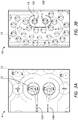
- Figure 4A is a schematic top plan view of a bump interface region 9 at or near the front side 7 of a package substrate 3, in which the bump interface region 9 is configured to connect to a transmission line structure of the die 2, according to various embodiments.
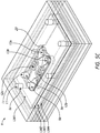
- Figure 4B is a schematic top plan view of a ball interface region 10 at or near the back side 8 of the package substrate 3, in which the ball interface region 10 is configured to connect to a transmission line structure of the system board 4, according to various embodiments.
- Figure 4C is a schematic top perspective view of the bump interface region 9 of Figure 4A .
- Figure 4D is a schematic top perspective view of the ball interface region 10 of Figure 4B .
- the bump interface region 9 can comprise the bump launch structure 15 in which vias 13a, 13b are provided from the uppermost LM1 layer at the front side 7 of the substrate 3 to the LM2 layer below (e.g ., a 1-2 via as illustrated), as shown in the schematic perspective view of Figure 4C .
- the vias 13a, 13b can connect LM1 to LM2.
- conductive pads 19a, 19b can be patterned to connect to the vias 13a, 13b.
- the pads 19a, 19b can be shaped to obtain a desirable voltage standing wave ratio (VSWR) for the interface region 9.
- VSWR voltage standing wave ratio
- Transmission lines can connect the pads 19a, 19b to additional vias 13, which can transfer the signals to lower layers of the substrate 3, the ball launch structure 16, and to layer BM1 of the system board 4 by way of the solder balls 6.
- the vias 13a, 13b can be separated within an insulating field region (not shown).
- the ball interface region 10 can comprise the ball launch structure 16 in which the vias 13c, 13d terminate at the back side 7 of the substrate 3 to connect to the solder balls 6, as shown in the schematic perspective view of Figure 4D .
- the vias 13c, 13d can be separated within an insulating field region (not shown).
- a plurality of launch metallic structures 112 can be shaped to transfer signals to corresponding vias 13 in the substrate 3.
- the vias 13 can transfer the signals down through the substrate 3 to the system board 4 by way of the solder balls 6 (see Figures 1A and 1B ). Vias 13' in the board 4 can transfer signals down through portions of the system board 4.
- the launch metallic structure 112 can be shaped to define a desired capacitance for the ball launch structure 16.
- the bump and ball launch structures 15, 16 of Figures 4A-4D can comprise patterns of metal and dielectric layer(s) that are structured so as to achieve an impedance that substantially matches the communication line(s) (e.g ., the transmission line(s)) of the die 2 and of the system board 4, respectively.
- the impedance Z die of the transmission line 30 of the die 2 can be determined. Based at least in part on the type of structure (e.g ., single ended or balanced), it can determine the mode(s) in which the package 1 is likely to be operated. Thus, in the illustrated embodiment, a balanced line structure is shown.
- estimated values for inductance ( L ) and/or capacitance ( C ) may be selected so as to approximate Z die (within a desired range).
- the layers of the bump and ball launch structures 15, 16 can be patterned so as to achieve the estimated L and/or C values, and, thus, the estimated impedance Z bump-launch , Z ball-launch for the respective bump and ball launch structures 15, 16.
- the compensation techniques disclosed herein can be suitable for a wide range of impedances and/or operational frequencies.
- a particular ball or bump launch structure can be designed.
- the designed ball or bump launch structure can be saved and used in additional, different packages that operate at similar frequencies or have other similar parameters.
- the capacitance C of the bump and ball launch structures 15, 16 can be tuned by appropriately selecting the diameter and/or spacings of the vias 13a, 13b, 13c, 13d.
- the spacing between vias 13a and 13b (and/or between vias 13c and 13d) can be adjusted to obtain a desired capacitance C for the launch structures.
- a gap 119 between the conductive pads 19a, 19b can be adjusted to achieve a desired capacitance C , for example, for the differential mode of operation (see Figure 4C ).
- a gap between portions of the launch metallic structures 112 can be adjusted to tune the capacitance C .
- a gap 120 between the conductive pads 19 and a ground plane defined by LM2 can be tuned to achieve a desired capacitance C , for example, for a common mode of operation.
- the vertical separation of the metallic layers can also be adjusted to achieve the desired capacitance C .
- the materials of the dielectric layers 14 can be further selected so as to achieve the desired capacitance C and impedances Z bump-launch , Z ball-launch .
- portions of the launch structures 15, 16 can be tuned to achieve a desired inductance L , to improve impedance matching.
- adjusting the spacing of the vias 13a-13d can change the inductance L of the launch structures 15, 16.
- the inductance L can be modified by changing the length of the vias 13a-13d. For example, in some embodiments, a higher inductance L may be achieved by increasing a length of a particular via 13.
- the vias 13 can be formed to pass through any number of metal layers LM or BM.
- the inductance L may be increased by increasing the number of metallic layers LM or BM through which the vias 13 are disposed ( e.g ., providing a via 13 between LM1 and LM4, as opposed to between LM1 and LM3).
- the inductance L can be tuned or adjusted by modifying the spacing between the conductive bumps 5a-5c (see Figure 4C ).
- bumps 5a and 5b can provide a signal pathway to the vias 13a, 13b.
- Bump 5c can provide a ground return path with the die 2. Adjusting the relative spacing between the bumps 5a, 5b, and 5c can also adjust the inductance L of the launch structures.
- Figures 5A-5E illustrate an embodiment of bump and ball launch structures 15, 16 that provide improved impedance matching for receiver line structures (not shown) of the die 2 and/or the system board 4.
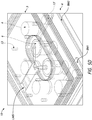
- Figure 5A is a schematic top plan view of a bump interface region 9 at or near the front side 7 of a package substrate 3, in which the bump interface region 9 is configured to connect to a receiver line structure of the die 2, according to various embodiments.
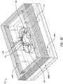
- Figure 5B is a schematic top plan view of a ball interface region 10 at or near the back side 8 of the package substrate 3, in which the ball interface region 10 is configured to connect to a receiver line structure of the system board 4, according to various embodiments.
- Figure 5C is a schematic top perspective view of the bump interface region 9 of Figure 5A .
- Figure 5D is a schematic top perspective view of the ball interface region 10 of Figure 5B , illustrating from metal layer 5 (LM5) of the package substrate 3 to board metal layer 2 (BM2) of the system board 4.
- Figure 5E is a schematic top perspective view of the ball interface region 10 of Figure 5B , illustrating from metal layer 2 (LM2) of the package substrate to board metal layer 2 (BM2) of the system board.
- the impedance Z die of the receiver line of the die 2 may differ from the impedance Z die of the transmission line of the die 2. Accordingly, different bump and ball launch structures 15, 16 can be utilized to compensate for the varying impedances.
- the bump and ball launch structures 15, 16 can comprise metallic structures that can serve as inductance generation elements 12a, 12b, 12c, 12d configured to electrically connect to receiver communication lines in the die 2 or board 4 (see Figures 1A and 1B ), respectively.
- the inductance generation elements 12a-12d can connect to corresponding vias 13a-13d for providing vertical communication through the substrate 3.
- the length and/or curvature of the inductance generation elements 12a-12d can be adjusted to achieve a desired inductance L for the launch structures.
- the inductance generation elements 12c, 12d may be longer and/or may have more turns than the inductance generation elements 12a, 12b, because, e.g ., additional inductance is desired.
- the inductance generation elements 12a-12d can be angled relative to one another so as to prevent interference with other components of the package or the larger electronic device.
- the inductance generation elements 12c, 12d can be angled approximately orthogonally relative to one another so as to reduce interference with other systems ( e.g ., to prevent electrical coupling with other structures).
- the inductance generation elements 12a, 12b of the bump launch structure 15 of Figure 5A may be disposed generally parallel to one another, for example, if there are no sensitive components vertically adjacent the elements 12a, 12b.
- the inductance generation elements 12a-12d can comprise any suitable length and/or turns so as to adjust inductance, and the elements 12a-12d can be angled suitably so as to reduce electrical coupling or interference with other components.
- one or more layers of the substrate 3 e.g., LM3
- the metallic layer e.g ., LM3
- the inductance generation elements 12a, 12b, 12c, 12d can comprise serpentine traces having a plurality of crests and troughs, e.g ., a wave-like shape.
- the length, width, and/or curvature of the inductance generation elements 12a-12d can be selected so as to provide a desired inductance ( L ) of the bump and/or ball launch structures 15, 16.
- the diameter and/or spacings of the vias 13 can be selected so as to provide a desired capacitance ( C ) of the bump and/or ball launch structures 15, 16.
- the embodiment of Figures 5A-5E can beneficially match the impedance(s) of an RF receiver line.
- the spacing of the bumps 5a-5c can be adjusted to tune the inductance of the launch structure 15.
- the length of the vias 13 can be adjusted, as explained above, to provide a desired inductance.
- the structures of Figures 5A-5E can generally be tuned in manners similar to those explained above in connection with Figures 4A-4D .
- tuning the capacitance ( C ) and/or inductance ( L ) of the bump and ball launch structures 15, 16 of Figures 4A-5E can define respective bump and ball impedances Z bump-launch , Z ball-launch , respectively, that substantially match the impedance Z die of the transmission line structure of the die 2, and/or the impedance Z board of the transmission line structures of the system board 4.
- the bump and ball launch impedances Z bump-launch , Z ball-launch can be substantially matched with the impedance Z die of the transmission line structure of the die 2 as explained above, and/or substantially matched with the impedance Z board of the transmission line structures of the system board 4 as explained above.
- the impedances can be matched at the operational frequencies of the die 2, e.g., at frequencies up to 75 GHz, or up to 60 GHz, e.g., at frequencies up to 40 GHz.
- the impedances can further be matched across the bandwidth (e.g ., a 0.5 dB bandwidth) of the operational frequency response, e.g ., matched across substantially the entirety of a 0.5 dB bandwidth of 75 GHz, or up to 60 GHz, e.g., up to 40 GHz.
- the impedances can be matched across the 0.5 dB bandwidth of the frequency response, e.g ., matched across a bandwidth in a range of DC to 75 GHz, in a range of 0.5 GHz to 75 GHz, in a range of DC to 60 GHz, in a range of 0.5 GHz to 60 GHz, in a range of 0.5 GHz to 45 GHz, in a range of 1 GHz to 40 GHz, or in a range of 2 GHz to 6 GHz.
- various ranges of operational frequencies are provided herein, it should be appreciated that the embodiments disclosed herein can be employed with structures configured to operate at any suitable frequency. For example, structures employing a lower dielectric constant may be able to operate at higher frequencies.
- Various embodiments disclosed herein can utilize dielectric materials having a dielectric constant in a range of about 3.3. to 4.6, e.g ., in a range of 3.3 to 3.8.
- Such structures can operate at frequencies in a range of DC to 75 GHz, in a range of DC to 60 GHz, in a range of 0.5 GHz to 60 GHz, in a range of 0.5 GHz to 50 GHz, or in a range of 0.5 GHz to 40 GHz.
- the bump and ball launch structures 15, 16 can enable impedance matching between the communications line(s) 30 (e.g ., transmission and/or receiver line(s)) of the die 2 and the substrate 3 ( e.g ., along the bump interface region 9), and between the substrate 3 and corresponding communication line(s) of the system board ( e.g ., along the ball interface region 10).
- the impedance matching can be configured to provide improved performance across a wide range of frequencies, such that the device die 2 can be operated across a wide range of frequencies without additional tuning to the system board 4.
- the die 2 and substrate 3 can be mounted to the system board 4 without providing additional tuning or other external components to tune the impedance.
- additional discrete components e.g ., passive devices, such as inductors, capacitors, resistors
- passive devices such as inductors, capacitors, resistors
- additional matching components may utilize package-specific calculations in order to match the impedance of the package components to the system board 4.
- the embodiments disclosed herein obviate the need for additional impedance matching components by matching the impedance Z die of the communications line(s) 30 of the die 2 to the impedance Z bump-launch of the bump launch structure 15, and by matching the impedance Z ball-launch of the ball launch structure 16 to the impedance of the system board Z board .
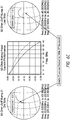
- Figure 6A illustrates a series of graphs (Smith charts) illustrating the performance of the bump launch structure 15 of Figure 5A for compensating the impedance of a receiver transmission line (approximately 100 ohm impedance), as compared with the performance of the bump launch structure of Figure 3A .
- the loci representative of the voltage standing wave ratio (VSWR) of the embodiment shown in Figure 5A shown in dashed line, can be substantially smaller than the VSWR of an uncompensated structure, shown in solid line.
- the VSWR of the structure shown in Figure 5A can be less than 2.5:1 for operational frequencies up to about 40 GHz, or less than 2:1.
- the VSWR of the bump launch structure shown in Figure 5A can be in a range of 1:1 to 1.95:1, in a range of 1:1 to 1.75:1, in a range of 1:1 to 1.5:1, or in a range of 1:1 to 1.25:1.
- Figure 6B illustrates a series of graphs illustrating the performance of the ball launch structure 16 of Figure 5B for compensating the impedance of a receiver transmission line (approximately 100 ohm impedance), as compared with the performance of the ball launch structure of Figure 3B .
- the smaller impedance loci (shown in dashed lines) indicates improved performance relative to other types of compensation structures (shown in solid lines).
- the VSWR of the ball launch structure shown in Figure 5B can be less than 2.5:1 for operational frequencies up to about 40 GHz, or less than 2.25:1.
- the VSWR of the ball launch structure shown in Figure 5B can be in a range of 1:1 to 1.95:1, in a range of 1:1 to 1.75:1, in a range of 1:1 to 1.5:1, or in a range of 1:1 to 1.25:1.
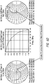
- Figure 6C illustrates a series of graphs illustrating the performance of the bump launch structure 15 of Figure 4A for compensating the impedance of a transmitter transmission line (approximately 50 ohm impedance), as compared with the bump launch structure of Figure 2A .
- the VSWR of the bump launch structure shown in Figure 4A shown in dashed line, can be less than 2:1, or less than 1.5:1 for operational frequencies up to about 40 GHz, or less than 1.3:1.
- the VSWR of the ball launch structure shown in Figure 4A can be in a range of 1:1 to 1.5:1, in a range of 1:1 to 1.25:1, in a range of 1:1 to 1.2:1, or in a range of 1:1 to 1.1:1
- Figure 6D illustrates a series of graphs illustrating the performance of the ball launch structure 16 of Figure 4B for compensating the impedance of a transmitter transmission line (approximately a 50 ohm impedance), as compared with the bump launch structure of Figure 2B .
- the graphs in Figures 6C-6D show a smaller impedance loci for the bump and ball launch structures 15, 16 disclosed herein, as compared with other structures.
- the VSWR of the ball launch structure shown in Figure 4B shown in dashed line, can be less than 3:1 for operational frequencies up to about 40 GHz, less than 2.5:1, or less than 2:1 for frequencies up to 40 GHz.
- the VSWR of the bump launch structure shown in Figure 4B can be in a range of 1:1 to 2.2:1, in a range of 1:1 to 2:1, or in a range of 1:1 to 1.75:1.
- the Smith charts of Figures 6A-6D illustrate that the bump and ball launch structures disclosed herein can beneficially improve impedance matching as compared with other, uncompensated structures.
Landscapes
- Engineering & Computer Science (AREA)
- Microelectronics & Electronic Packaging (AREA)
- Production Of Multi-Layered Print Wiring Board (AREA)
- Physics & Mathematics (AREA)
- Geometry (AREA)
- Combinations Of Printed Boards (AREA)
Abstract
Description
- This application claims the benefit of
U.S. Provisional Application No. 62/677,549 - The field relates to launch structures for radio frequency integrated device packages.
- Radio frequency (RF) integrated device dies and packages are used for high frequency communication applications, including radio-on-chip products, for wirelessly transmitting and/or receiving RF signals. The RF integrated device die can be mounted to a package substrate for incorporation into a larger electronic device or system. However, in some arrangements, the electrical interface between the integrated device die and the package substrate, or between the package substrate and the larger system, may be inefficient so as to produce losses that degrade the performance of the system. Accordingly, there remains a continuing need for improved RF integrated device packages.
- In one aspect, an integrated device package is disclosed. The integrated device package includes a laminate substrate that has a front side and a back side. The laminate substrate includes a plurality of layers. The integrated device package also includes an integrated device die that is mounted to the front side of the laminate substrate. The integrated device die includes radio frequency (RF) circuitry and has a first impedance. The integrated device die operates at one or more operational frequencies. The integrated device package further includes a plurality of conductive bumps that are disposed between the integrated device die and the front side of the laminate substrate. The conductive bumps are electrically connects the integrated device die and the laminate substrate. The integrated device package further includes a bump launch structure that is defined at least in part by one or more layers at or near the front side of the laminate substrate. The bump launch structure includes metallic and insulating materials that are arranged in a first pattern that has a second impedance that is matched to the first impedance such that a voltage standing wave ratio (VSWR) of the bump launch structure is less than 4:1.
- In one embodiment, the integrated device package further includes a ball launch structure that is defined at least in part by one or more layers at or near the back side of the laminate substrate. The ball launch structure can include metallic and insulating materials arranged in a second pattern having a third impedance. The integrated device package can further include one or more traces or vias that electrically connect the first pattern of the bump launch structure and the second pattern of the ball launch structure. The integrated device package can further include a plurality of solder balls that are electrically and mechanically connected to the back side of the laminate substrate. The ball launch structure can further include the plurality of solder balls. The integrated device package can further include a system board that has a fourth impedance. The laminate substrate can be mounted to a front side of the system board by way of the plurality of solder balls. The ball launch structure can further include one or more layers at or near the front side of the system board. The third and fourth impedances can be matched such that a voltage standing wave ratio (VSWR) of the ball launch structure is less than 5:1. At least one of the bump launch structure and the ball launch structure can include a plurality of metallic vias spaced apart by an insulator. The plurality of metallic vias can extend through one or more layers of the laminate substrate. Spacings between adjacent metallic vias can define a corresponding capacitance that defines at least in part the second impedance or the third impedance. At least one of the bump launch structure and the ball launch structure can include a serpentine metallic trace electrically connected with a metallic via. The metallic via can extend through one or more layers of the laminate substrate.
- In one embodiment, wherein the bump launch structure further includes the plurality of conductive bumps.
- In one embodiment, the integrated device die includes an underbump metallization (UBM) layer. The plurality of conductive bumps can be connected to the UBM layer. The bump launch structure can further include the UBM layer.
- In one embodiment, wherein the one or more operational frequencies includes frequencies in a range of 0.5 GHz to 60 GHz.
- In one embodiment, the RF circuitry of the integrated device die operates over a 0.5 dB bandwidth of frequencies, The second impedance can be substantially matched to the first impedance across the bandwidth. The 0.5 dB bandwidth can be in a range of DC to 75 GHz.
- In one aspect, a laminate substrate for supporting a radio frequency (RF) integrated device die that is configured to operate at one or more operational frequencies is disclosed. The laminate substrate has a front side and a back side opposite the front side. The laminate substrate includes a bump launch structure that is defined at least in part by one or more layers at or near the front side of the laminate substrate. The bump launch structure includes metallic and insulating materials that are arranged in a first pattern having a first impedance at the one or more operational frequencies. The first impedance of the bump launch structure is configured to substantially match an impedance of the RF integrated device die that has radio frequency (RF) circuitry. The laminate substrate also includes a ball launch structure that is defined at least in part by one or more layers at or near the back side of the laminate substrate. The ball launch structure includes metallic and insulating materials that are arranged in a second pattern having a second impedance at the one or more operational frequencies. The second impedance of the ball launch structure is configured to substantially match an impedance of a system board. The laminate substrate further includes one or more traces or vias that electrically connect the bump launch structure and the ball launch structure.
- In one embodiment, the laminate substrate further includes a plurality of solder balls electrically and mechanically connected to the back side of the laminate substrate. The ball launch structure can further include the plurality of solder balls.
- In one embodiment, the one or more operational frequencies are in a range of DC to 75 GHz.
- In one embodiment, at least one of the bump launch structure and the ball launch structure includes a plurality of metallic vias spaced apart by an insulator. The plurality of metallic vias can extend through one or more layers of the laminate substrate.
- In one embodiment, at least one of the bump launch structure and the ball launch structure can include a serpentine metallic trace electrically connected with a metallic via. The metallic via can extend through one or more layers of the laminate substrate.
- In one aspect, an electronic device is disclosed. The electronic device includes a system board that has a first radio frequency (RF) communications line. The first RF communications line has a first impedance at one or more operational frequencies. The electronic device also includes a laminate substrate that is mounted to the system board. The laminate substrate has a front side and a back side opposite the front side. The electronic device also include a plurality of solder balls that are disposed between the system board and the back side of the laminate substrate. The solder balls electrically connect the system board and the laminate substrate. The electronic device further includes a ball launch structure that is defined at least in part by one or more layers at or near the back side of the laminate substrate. The ball launch structure includes metallic and insulating materials that are arranged in a first pattern that has a second impedance at the one or more operational frequencies. The second impedance of the ball launch structure is matched to the first impedance of the first RF communications line such that a voltage standing wave ratio (VSWR) of the ball launch structure is less than 5:1.
- In one embodiment, the electronic device further includes an integrated device die that is mounted to the laminate substrate by way of one or more conductive bumps. The integrated device die can include radio frequency (RF) circuitry and have a third impedance. The electronic device can further include a bump launch structure that is defined at least in part by one or more layers at or near the front side of the laminate substrate. The bump launch structure can include metallic and insulating materials that are arranged in a second pattern that has a fourth impedance that is matched to the third impedance such that a voltage standing wave ratio (VSWR) of the bump launch structure is less than 3:1.
- Specific implementations of the invention will now be described with reference to the following drawings, which are provided by way of example, and not limitation.
-
Figure 1A is a schematic side sectional view of an RF integrated device package, according to various embodiments. -
Figure 1B is a schematic side sectional view of bump and ball interface regions that can comprise bump and ball launch structures, according to various embodiments. -
Figure 2A is a schematic top plan view of a bump interface region at or near the front side of a package substrate, in which the bump interface region is configured to connect to a transmission line structure of the die. -
Figure 2B is a schematic top plan view of a ball interface region at or near the back side of the package substrate, in which the ball interface region is configured to connect to a transmission line structure of the system board. -
Figure 3A is a schematic top plan view of a bump interface region at or near the front side of a package substrate, in which the bump interface region is configured to connect to a receiver line structure of the die which is connected to the receiver of the die. -
Figure 3B is a schematic top plan view of a ball interface region at or near the back side of the package substrate, in which the ball interface region is configured to connect to a receiver line structure of the system board. -
Figure 4A is a schematic top plan view of a bump interface region at or near the front side of a package substrate, in which the bump interface region is configured to connect to a transmission line structure of the die, according to various embodiments. -
Figure 4B is a schematic top plan view of a ball interface region at or near the back side of the package substrate, in which the ball interface region is configured to connect to a transmission line structure of the system board, according to various embodiments. -
Figure 4C is a schematic top perspective view of the bump interface region ofFigure 4A . -
Figure 4D is a schematic top perspective view of the ball interface region ofFigure 4B . -
Figure 5A is a schematic top plan view of a bump interface region at or near the front side of a package substrate, in which the bump interface region is configured to connect to a receiver line structure of the die, according to various embodiments. -
Figure 5B is a schematic top plan view of a ball interface region at or near the back side of the package substrate, in which the ball interface region is configured to connect to a receiver line structure of the system board, according to various embodiments. -
Figure 5C is a schematic top perspective view of the bump interface region ofFigure 5A . -
Figure 5D is a schematic top perspective view of the ball interface region ofFigure 5B . -
Figure 5E is a schematic top perspective view of the ball interface region ofFigure 5B , illustrating from metal layer of the package substrate to board metal layer of the system board. -
Figure 6A illustrates plot showing the electrical performance of the bump and ball compensation or launch structures disclosed herein, according to one embodiment. -
Figure 6B illustrates plot showing the electrical performance of the bump and ball compensation or launch structures disclosed herein, according to another embodiment. -
Figure 6C illustrates plot showing the electrical performance of the bump and ball compensation or launch structures disclosed herein, according to another embodiment. -
Figure 6D illustrates plot showing the electrical performance of the bump and ball compensation or launch structures disclosed herein, according to another embodiment. - Various embodiments disclosed herein relate to radio frequency (RF) integrated device packages and for launch structures that improve the performance of wireless communications systems.
Figure 1A is a schematic side sectional view of an RFintegrated device package 1, according to various embodiments. TheRF package 1 can include an RF integrated device die 2 configured to operate at one or more operational frequencies, e.g., frequencies in a range of 0 Hz to 40 GHz, or up to 60 GHz. The RF integrated device die 2 can be mounted and electrically connected to afront side 7 of apackage substrate 3 by way of one or a plurality of conductive bumps 5 (e.g., solder bumps, copper pillars, etc.) provided at aback side 33 of thedie 2, for example, in a flip chip mounting technique. In various embodiments, active circuitry of thedie 2 may be provided at or near theback side 33 of thedie 2. In some embodiments, active circuitry of thedie 2 may be provided at or near an oppositefront side 35 of thedie 2. Thepackage substrate 3 can comprise any suitable type of package substrate, including, e.g., a laminate substrate (such as a printed circuit board, or PCB), a ceramic substrate, etc. In the illustrated embodiment, thesubstrate 3 comprises a laminate substrate with multiple patterned metal and dielectric layers LM1, LM2, ... LMn. Aback side 8 of thepackage substrate 3 can be mounted to afront side 31 of the system board 4 (e.g., motherboard) by way of a plurality ofsolder balls 6. Thesystem board 4 can serve as an interface to a larger electronic device or system. - The RF integrated device die 2 can comprise one or a plurality of communications lines. In some embodiments, for example, the RF integrated device die 2 can comprise a
receiver 17 configured to receive and process signals transmitted from another device, and/or atransmitter 18 configured to transmit signals wirelessly to another device. Thereceiver 17 can electrically connect to the conductive bump(s) 5 by way of a receiver line structure (not shown) defined in thedie 2, and thetransmitter 18 can electrically connect to the conductive bump(s) 5 by way of a transmitter line structure (not shown) defined in thedie 2. The communication line structures (e.g., the respective receiver and/or transmitter line structures) may have associated impedance(s) at the operational frequencies of the package. Electrical signals can pass between the communication lines of thedie 2 and upper metallic layer(s) of thepackage substrate 3 by way of theconductive bumps 5. The signals can pass through the package substrate 3 (e.g., through patterned metallic traces and vias). The signals can pass between thepackage substrate 3 and thesystem board 4 by way of thesolder balls 6. In some embodiments, thedie 2 can comprise areceiver 17 but no transmitter, while in other embodiments, thedie 2 can comprise atransmitter 18 but no receiver. In some embodiments, thedie 2 can comprise both thereceiver 17 and thetransmitter 18. In some embodiments, thedie 2 can comprisemultiple receivers 17 and/ormultiple transmitters 18. In various embodiments, thedie 2 can comprise one or more high speed digital links (e.g., JESD204 links) that can serve as a high speed digital interface. - As shown in
Figure 1A , thepackage 1 can comprise abump interface region 9 that defines an electrical interface between theback side 33 of thedie 2 and thefront side 7 of thepackage substrate 3, and aball interface region 10 that defines an electrical interface between theback side 8 of thepackage substrate 3 and thefront side 31 of thesystem board 4. In some packages, thebump interface region 9 may provide poor impedance matching between the communications lines of thereceiver 17 and/ortransmitter 18 on thedie 2 and corresponding metallic pads on thefront side 7 of thesubstrate 3. Similarly, in some packages, theball interface region 10 may provide poor impedance matching between metallic pads on theback side 8 of thepackage substrate 3 and corresponding pads on thesystem board 4. In such packages with mismatched impedance(s), the electrical performance of thepackage 1 can be significantly degraded. For example, a substantial amount of electrical energy can be lost due to parasitic effects in packages with mismatched impedance(s) at the bump orball interface regions - Accordingly, in various embodiments disclosed herein, the
bump interface region 9 can comprise a bump launch structure 15 (seeFigure 1B ) that substantially matches the impedance of the communications lines (e.g., the transmitter and/or receiver lines) formed in thedie 2 with the impedance of the metallic traces and/or vias of thepackage substrate 3, across the operational frequency(ies) of thepackage 1. Similarly, in various embodiments, theball interface region 10 can comprise a ball launch structure 16 (seeFigure 1B ) that substantially matches the impedance of the metallic traces and/or vias of thepackage substrate 3 with the impedance of the metallic pads of thesystem board 4, across the operational frequency(ies) of thepackage 1. By matching the impedances at the bump andball interface regions ball interfaces launch structures package 1 by tuning the system inductance and capacitance to account for parasitic losses, e.g., capacitive losses, etc. -
Figure 1B is a schematic side sectional view of the bump andball interface regions ball launch structures Figure 1B illustrates a lower portion of the integrated device die 2, thepackage substrate 3, thesystem board 4, aconductive bump 5 between and connecting the integrated device die 2 and thepackage substrate 3, and asolder ball 6 between and connecting thepackage substrate 3 and thesystem board 4. As shown inFigure 1B , the integrated device die 2 can comprise an underbump metallization (UBM)layer 11 disposed at theback side 33 of thedie 2. TheUBM layer 11 can serve as an electrical interface between thedie 2 and thesubstrate 3. Furthermore, inFigure 1B , thedie 2 can comprise acommunications line structure 30 that provides electrical communication between theUBM layer 11 and thereceiver 17 or transmitter 18 (not shown inFigure 1B ). As explained herein, thecommunications line structure 30 can comprise a receiver line that connects to a receiver, or a transmission line that connects to a transmitter. Thecommunication structure 30 of thedie 2 can have an impedance Zdie which may vary with the operational frequency. Further, thedie 2 can comprise various types of circuitry, including, e.g., transistors for the receiver and/or transmitter, and/or for high speed digital interfaces. - As shown in
Figure 1B , thepackage substrate 3 can comprise a multilayered laminate substrate comprising a plurality of patterned metal layers (or laminate metal layers, LMx) LM1 ... LMn. For example, as shown inFigure 1B , the patterned layers can comprise a plurality ofmetallic traces 12 that extend laterally along a particular layer LMn and a plurality ofmetallic vias 13 that extend vertically to connecttraces 12 in other layers LMn. Thus, as illustrated, thetraces 12 can transfer electrical signals laterally or horizontally in the substrate 3 (e.g., generally parallel to a major lateral dimension of the substrate 3), and thevias 13 can transfer electrical signals vertically in the substrate 3 (e.g., generally non-parallel or perpendicular to the major lateral dimension of the substrate 3). InFigure 1B , each via 13 is illustrated as connecting a particular layer to a layer directly above or below that particular layer, but in other embodiments, thevias 13 can pass through multiple layers, or through the entirety of the thickness of thesubstrate 3. An insulatingdielectric material 14 can electrically separate portions of thevias 13 and traces 12. Thus, each layer of thesubstrate 3 can comprise a pattern defined by the arrangement of metal (e.g., whether a via 13 or trace 12) anddielectric 14 for that layer. Further, inFigure 1B , the illustrated portion of thesystem board 4 may also include one or more board layers BM1, ... BMm comprising one or a plurality of patterned metal and dielectric layers. The illustratedboard 4 may also comprise a laminate substrate, according to some embodiments. Any suitable metal can be used for thetraces 12 andvias 13, including, e.g., aluminum, copper, etc. Any suitable insulator can be used for the dielectric 14, including, e.g., FR-4 board, an epoxy, a ceramic, glass, etc. - In various packaging arrangements, the
bump interface region 9 may introduce an electrical transition between thecommunication line 30 in thedie 2 and the metallic layers of thepackage substrate 3. In such an electrical transition, the impedance Zdie of thecommunications line 30 of thedie 2 may differ from an impedance Zbump of thebump 5, an impedance Zs1 at or near thefront side 7 of thesubstrate 3, and/or an impedance of other structures in thesubstrate 3. Similarly, an impedance Zs2 at or near theback side 8 of thesubstrate 3 may differ from an impedance Zball of thesolder ball 6 and/or an impedance Zboard at or near thefront side 31 of the system board 4 (e.g., at BM1, BM2, and/or the intervening dielectric 14). In instances in which the impedances are mismatched, significant electrical energy can be lost due to, e.g., parasitic effects, which can degrade overall RF performance. - Accordingly, in various embodiments disclosed herein, the
bump interface region 9 can comprise thebump launch structure 15, which can comprise various layer(s) of thedie 2, the conductive bump(s) 5, and various layer(s) at or near thefront side 7 of thepackage substrate 3. In the illustrated embodiment, for example, thebump launch structure 15 can comprise theUBM layer 11 of thedie 2, the bump(s) 5, thetraces 12 at layers LM1 and LM2, and the via 13 connecting thetraces 12 at LM1 and LM2. In other embodiments, however, thebump launch structure 15 can comprise more or fewer layers and/or structures. For example, in other embodiments, thebump launch structure 15 can comprise only layer(s) in thepackage substrate 3. Still other combinations may be suitable. An overall impedance Zbump-launch of thebump launch structure 15 can be selected so as to substantially match the impedance Zdie of the communication line(s) 30 of thedie 2. For example, as explained herein, the shapes, sizes, and/or spaces of thetraces 12 and vias 13 can be selected so as to create a desired effective inductance and/or capacitance, which can result in a substantially matched impedance. In such embodiments, for example, the overall impedance Zbump-launch of thebump launch structure 15 can be selected such that the voltage standing wave ratio (VSWR) is less than 4:1, less than 3:1, less than 2:1 or less than 1.5:1. For example, the overall impedance Zbump-launch of thebump launch structure 15 can be selected such that the voltage standing wave ratio (VSWR) is in a range of 1:1 to 4:1, in a range of 1.05:1 to 4:1, in a range of 1:1 to 3:1, in a range of 1.05:1 to 3:1, in a range of 1:1 to 2.5:1, in a range of 1.05:1 to 2.5:1, in a range of 1:1 to 2:1 or in a range of 1.05:1 to 2:1, e.g., in a range of 1:1 to 1.75:1, in a range of 1:1 to 1.5:1, or in a range of 1.25:1 to 1.75:1. - Similarly, in various embodiments disclosed herein, the
ball interface region 10 can comprise theball launch structure 16, which can comprise various layer(s) at or near theback side 8 of thepackage substrate 3, the solder ball(s) 6, and various layer(s) at or near thefront side 31 of thesystem board 4. In the illustrated embodiment, for example, theball launch structure 16 can comprise thetrace 12 at LM6 and the via 13 thereabove, the ball(s) 6, and thetraces 12 and vias 13 at layers BM1 and BM2 of theboard 4. In other embodiments, however, theball launch structure 16 can comprise more or fewer layers and/or structures. For example, in other embodiments, theball launch structure 16 can comprise only layer(s) in thepackage substrate 3. Still other combinations may be suitable. An overall impedance Zball-launch of theball launch structure 16 can be selected so as to substantially match the impedance Zboard of communication line structure(s) in thesystem board 4. For example, as explained herein, the shapes, sizes, and/or spaces of thetraces 12 and vias 13 in thesubstrate 3 can be selected so as to create a desired effective inductance and/or capacitance, which can result in a substantially matched impedance. In such embodiments, for example, the overall impedance Zball-launch of theball launch structure 16 can be selected such that the voltage standing wave ratio (VSWR) is less than 5:1, less than 4:1, less than 3:1 or less than 2.5:1. For example, the overall impedance Zbump-launch of theball launch structure 16 can be selected such that the voltage standing wave ratio (VSWR) is in a range of 1:1 to 5:1, in a range of 1.05:1 to 5:1, in a range of 1:1 to 4:1, in a range of 1.05:1 to 4:1, in a range of 1:1 to 3.5:1, in a range of 1.05:1 to 3.5:1, in a range of 1:1 to 3:1, in a range of 1:1 to 2:1, e.g., in a range of 1:1 to 1.75:1, in a range of 1:1 to 1.5:1, or in a range of 1.25:1 to 1.75:1. -
Figure 2A is a schematic top plan view of abump interface region 9 at or near thefront side 7 of thepackage substrate 3 illustrated inFigures 1A and1B , in which thebump interface region 9 is configured to connect to a transmission line structure of the die 2 (seeFigure 1A ), which communicates with the transmitter 18 (seeFigure 1A ).Figure 2B is a schematic top plan view of aball interface region 10 at or near theback side 8 of thepackage substrate 3 illustrated inFigures 1A and1B , in which theball interface region 10 is configured to connect to a transmission line structure of the system board 4 (seeFigure 1A ).Figures 2A-2B illustrate only metallic or conductive structures of the bump andball interface regions dielectric material 14 shown inFigure 1B . Thedielectric material 14 may be disposed in the regions ofFigures 2A-2B shown as voids. As shown inFigures 2A-2B , the bump andball interface regions conductive traces 12 and vias 13 separated by intervening insulating or dielectric material (not shown inFigures 2A-2B ). In the arrangement ofFigures 2A-2B , layers illustrated in shadow underlie upper layers of thesubstrate 3. - As shown in
Figure 2A , thebump interface region 9 can comprise a pair of transmission traces 12a, 12b connected to correspondingvias 13 that pass through at least a portion of the thickness of thesubstrate 3. The pair oftraces Figures 2A-2B (and indeed the other figures), vias that include numbers, such as 1-2, 2-3, or 2-5 illustrate the layers LM that thevias 13 electrically connect. For example, a via 13 with the label 1-2 over it provides electrical communication between layers LM1 and LM2. A via 13 with the label 2-3 provides electrical communication between layers LM2 and LM3. A via 13 with the label 2-5 provides electrical communication between layers LM2 and LM5, and so on. Thus, the transmission traces 12a, 12b at layer LM1 inFigure 2A provide electrical communication between the bump (not shown inFigure 2A ) and the correspondingvias 13 for the transfer of a transmission electrical signal that is to be wirelessly transmitted to another device. The transmission signal may be transferred from thetraces Figure 2A . The signal can communicate with theback side 8 of thesubstrate 3 by way of other traces and vias, which are not illustrated inFigure 2A . - In the arrangement of
Figure 2A , thebump interface region 9 can have an associated impedance Zbump-interface that is mismatched from the impedance of the transmission lines (e.g., the communications line structure 30) of the die 2 (not shown inFigure 2A ). For example, in some packages, the transmission lines of thedie 2 may have a nominal impedance value Zdie in a range of about 30 Ω to 60 Ω, e.g., an impedance Zdie of about 50 Ω. The impedance Zbump-interface may have an impedance that differs from the transmission line impedance Zdie such that the VSWR of the bump interface may be in a range of 3:1 to 5:1, or higher. For example, the transmission traces 12a, 12b ofFigure 2A can comprise relatively straight metallic structures that provide the shortest physical distance between thebump 5 and thevias 13. Moreover, the diameter and/or spacings of thevias 13 may not be selected to achieve a desired capacitance representative of an overall desired impedance. Thus, as explained above, the resulting impedance mismatch may result in reduced electrical performance of thepackage 1. - Similarly, the
ball interface region 10 ofFigure 2B can comprise a pair of transmission traces 12c, 12d that connect to correspondingvias 13 at or near theback side 8 of thesubstrate 3, e.g., by way of two 2-6 vias that connect LM2 with LM6. As with thebump interface region 9, the transmission traces 12c, 12d may be relatively straight, and the diameter and/or spacing of thevias 13 may not be selected so as to achieve a desired capacitance. As with thebump interface region 10, the structures ofFigure 2B may result in an impedance mismatch relative to transmission lines in the system board 4 (not shown), which can further degrade overall electrical performance. -
Figure 3A is a schematic top plan view of abump interface region 9 at or near thefront side 7 of apackage substrate 3 illustrated inFigures 1A and1B , in which thebump interface region 9 is configured to connect to a receiver line structure of the die 2 (not shown) which is connected to thereceiver 17 of the die 2 (seeFigure 1A ).Figure 3B is a schematic top plan view of aball interface region 10 at or near theback side 8 of thepackage substrate 3, in which theball interface region 10 is configured to connect to a receiver line structure of the system board 4 (not shown). Unless otherwise noted, components ofFigures 3A-3B may refer to components that are the same as or generally similar to like-numbered components ofFigures 1A-2B . As withFigures 2A-2B ,Figures 3A-3B illustrate only metallic or conductive structures of the bump andball interface regions dielectric material 14 shown inFigure 1B . Thedielectric material 14 may be disposed in the regions ofFigures 3A-3B shown as voids. For example, as withFigures 2A-2B , the bump andball interface regions receiver traces bump 5 at or near thefront side 7 of thesubstrate 3 to theball 6 at or near theback side 8 of thesubstrate 3. However, in various arrangements, the impedance Zdie of the receiver communications line that communicates with thereceiver 17 may have a different impedance than that of the transmitter communications line that communicates with thetransmitter 18. For example, in various arrangements, the impedance Zdie of the receiver communications line of thedie 2 may be in a range of 80 Ω to 120 Ω, e.g., about 100 Ω in some arrangements. - As with the
interface regions Figures 2A-2B , theinterface regions Figures 3A-3B for the receiver lines may have respective impedances Zbump-interface , Zball-interface that are mismatched from the respective receiver communication lines of thedie 2 and/or thesystem board 4, respectively. The resulting mismatch in impedance(s) can reduce signal quality and degrade system performance. -
Figures 4A-4D illustrate an embodiment of bump andball launch structures die 2 and/or the system board 4 (seeFigures 1A and1B ). In particular,Figure 4A is a schematic top plan view of abump interface region 9 at or near thefront side 7 of apackage substrate 3, in which thebump interface region 9 is configured to connect to a transmission line structure of thedie 2, according to various embodiments.Figure 4B is a schematic top plan view of aball interface region 10 at or near theback side 8 of thepackage substrate 3, in which theball interface region 10 is configured to connect to a transmission line structure of thesystem board 4, according to various embodiments.Figure 4C is a schematic top perspective view of thebump interface region 9 ofFigure 4A .Figure 4D is a schematic top perspective view of theball interface region 10 ofFigure 4B . - As shown in
Figure 4A , thebump interface region 9 can comprise thebump launch structure 15 in which vias 13a, 13b are provided from the uppermost LM1 layer at thefront side 7 of thesubstrate 3 to the LM2 layer below (e.g., a 1-2 via as illustrated), as shown in the schematic perspective view ofFigure 4C . As shown inFigure 4C , for example, thevias vias interface region 9. Transmission lines can connect the pads 19a, 19b toadditional vias 13, which can transfer the signals to lower layers of thesubstrate 3, theball launch structure 16, and to layer BM1 of thesystem board 4 by way of thesolder balls 6. Thevias ball interface region 10 can comprise theball launch structure 16 in which thevias back side 7 of thesubstrate 3 to connect to thesolder balls 6, as shown in the schematic perspective view ofFigure 4D . Thevias Figure 4D , a plurality of launchmetallic structures 112 can be shaped to transfer signals to correspondingvias 13 in thesubstrate 3. Thevias 13 can transfer the signals down through thesubstrate 3 to thesystem board 4 by way of the solder balls 6 (seeFigures 1A and1B ). Vias 13' in theboard 4 can transfer signals down through portions of thesystem board 4. The launchmetallic structure 112 can be shaped to define a desired capacitance for theball launch structure 16. - Beneficially, the bump and
ball launch structures Figures 4A-4D can comprise patterns of metal and dielectric layer(s) that are structured so as to achieve an impedance that substantially matches the communication line(s) (e.g., the transmission line(s)) of thedie 2 and of thesystem board 4, respectively. To pattern thelaunch structures transmission line 30 of thedie 2 can be determined. Based at least in part on the type of structure (e.g., single ended or balanced), it can determine the mode(s) in which thepackage 1 is likely to be operated. Thus, in the illustrated embodiment, a balanced line structure is shown. For the likely operating mode(s) (e.g., common or differential mode), the inductance (L) and capacitance (C) of the respective bump andball launch structures ball launch structure Figures 4A-4D ), estimated values for inductance (L) and/or capacitance (C) may be selected so as to approximate Zdie (within a desired range). Based at least in part on the estimated values for L and/or C, the layers of the bump andball launch structures ball launch structures - In the embodiment of
Figures 4A-4D , for example, the capacitance C of the bump andball launch structures vias vias vias gap 119 between the conductive pads 19a, 19b can be adjusted to achieve a desired capacitance C, for example, for the differential mode of operation (seeFigure 4C ). Similarly, a gap between portions of the launch metallic structures 112 (seeFigure 4D ) can be adjusted to tune the capacitance C. In some embodiments, agap 120 between the conductive pads 19 and a ground plane defined by LM2 (seeFigure 4C ) can be tuned to achieve a desired capacitance C, for example, for a common mode of operation. In some embodiments, the vertical separation of the metallic layers can also be adjusted to achieve the desired capacitance C. In some embodiments, the materials of thedielectric layers 14 can be further selected so as to achieve the desired capacitance C and impedances Zbump-launch , Zball-launch. - In various embodiments, portions of the
launch structures vias 13a-13d can change the inductance L of thelaunch structures vias 13a-13d. For example, in some embodiments, a higher inductance L may be achieved by increasing a length of a particular via 13. Similarly, to modify the inductance L, thevias 13 can be formed to pass through any number of metal layers LM or BM. For example, in some embodiments, the inductance L may be increased by increasing the number of metallic layers LM or BM through which thevias 13 are disposed (e.g., providing a via 13 between LM1 and LM4, as opposed to between LM1 and LM3). As another example, the inductance L can be tuned or adjusted by modifying the spacing between theconductive bumps 5a-5c (seeFigure 4C ). InFigure 4C , bumps 5a and 5b can provide a signal pathway to thevias Bump 5c can provide a ground return path with thedie 2. Adjusting the relative spacing between thebumps -
Figures 5A-5E illustrate an embodiment of bump andball launch structures die 2 and/or thesystem board 4. In particular,Figure 5A is a schematic top plan view of abump interface region 9 at or near thefront side 7 of apackage substrate 3, in which thebump interface region 9 is configured to connect to a receiver line structure of thedie 2, according to various embodiments.Figure 5B is a schematic top plan view of aball interface region 10 at or near theback side 8 of thepackage substrate 3, in which theball interface region 10 is configured to connect to a receiver line structure of thesystem board 4, according to various embodiments.Figure 5C is a schematic top perspective view of thebump interface region 9 ofFigure 5A .Figure 5D is a schematic top perspective view of theball interface region 10 ofFigure 5B , illustrating from metal layer 5 (LM5) of thepackage substrate 3 to board metal layer 2 (BM2) of thesystem board 4.Figure 5E is a schematic top perspective view of theball interface region 10 ofFigure 5B , illustrating from metal layer 2 (LM2) of the package substrate to board metal layer 2 (BM2) of the system board. As noted above, the impedance Zdie of the receiver line of thedie 2 may differ from the impedance Zdie of the transmission line of thedie 2. Accordingly, different bump andball launch structures - Unless otherwise noted, components of
Figures 5A-5E may be the same as or similar to like numbered components ofFigures 1A-4D . For example, as shown inFigures 5A-5B , the bump andball launch structures inductance generation elements die 2 or board 4 (seeFigures 1A and1B ), respectively. Further, theinductance generation elements 12a-12d can connect tocorresponding vias 13a-13d for providing vertical communication through thesubstrate 3. Beneficially, the length and/or curvature of theinductance generation elements 12a-12d can be adjusted to achieve a desired inductance L for the launch structures. For example, theinductance generation elements inductance generation elements inductance generation elements 12a-12d can be angled relative to one another so as to prevent interference with other components of the package or the larger electronic device. For example, in theball launch structure 16 ofFigure 5B , theinductance generation elements inductance generation elements bump launch structure 15 ofFigure 5A may be disposed generally parallel to one another, for example, if there are no sensitive components vertically adjacent theelements inductance generation elements 12a-12d can comprise any suitable length and/or turns so as to adjust inductance, and theelements 12a-12d can be angled suitably so as to reduce electrical coupling or interference with other components. Further, as shown inFigure 5C , one or more layers of the substrate 3 (e.g., LM3) can include aground cutout region 20, in which the metallic layer, e.g., LM3, is patterned so as to further tune, for example, capacitance of thelaunch structure 15. - In the embodiment of
Figures 5A-5E , theinductance generation elements inductance generation elements 12a-12d can be selected so as to provide a desired inductance (L) of the bump and/orball launch structures ball launch structures die 2. Beneficially, as with the embodiment ofFigures 4A-4D for compensating the impedance(s) of an RF transmission line, the embodiment ofFigures 5A-5E can beneficially match the impedance(s) of an RF receiver line. For example, as withFigures 4A-4D , inFigures 5A-5E , the spacing of thebumps 5a-5c can be adjusted to tune the inductance of thelaunch structure 15. Further, the length of the vias 13 can be adjusted, as explained above, to provide a desired inductance. The structures ofFigures 5A-5E can generally be tuned in manners similar to those explained above in connection withFigures 4A-4D . - Beneficially, tuning the capacitance (C) and/or inductance (L) of the bump and
ball launch structures Figures 4A-5E can define respective bump and ball impedances Zbump-launch , Zball-launch , respectively, that substantially match the impedance Zdie of the transmission line structure of thedie 2, and/or the impedance Zboard of the transmission line structures of thesystem board 4. For example, the bump and ball launch impedances Zbump-launch , Zball-launch can be substantially matched with the impedance Zdie of the transmission line structure of thedie 2 as explained above, and/or substantially matched with the impedance Zboard of the transmission line structures of thesystem board 4 as explained above. The impedances can be matched at the operational frequencies of thedie 2, e.g., at frequencies up to 75 GHz, or up to 60 GHz, e.g., at frequencies up to 40 GHz. The impedances can further be matched across the bandwidth (e.g., a 0.5 dB bandwidth) of the operational frequency response, e.g., matched across substantially the entirety of a 0.5 dB bandwidth of 75 GHz, or up to 60 GHz, e.g., up to 40 GHz. In various embodiments, the impedances can be matched across the 0.5 dB bandwidth of the frequency response, e.g., matched across a bandwidth in a range of DC to 75 GHz, in a range of 0.5 GHz to 75 GHz, in a range of DC to 60 GHz, in a range of 0.5 GHz to 60 GHz, in a range of 0.5 GHz to 45 GHz, in a range of 1 GHz to 40 GHz, or in a range of 2 GHz to 6 GHz. Although various ranges of operational frequencies are provided herein, it should be appreciated that the embodiments disclosed herein can be employed with structures configured to operate at any suitable frequency. For example, structures employing a lower dielectric constant may be able to operate at higher frequencies. Various embodiments disclosed herein can utilize dielectric materials having a dielectric constant in a range of about 3.3. to 4.6, e.g., in a range of 3.3 to 3.8. Such structures can operate at frequencies in a range of DC to 75 GHz, in a range of DC to 60 GHz, in a range of 0.5 GHz to 60 GHz, in a range of 0.5 GHz to 50 GHz, or in a range of 0.5 GHz to 40 GHz. - Advantageously, therefore, the bump and
ball launch structures die 2 and the substrate 3 (e.g., along the bump interface region 9), and between thesubstrate 3 and corresponding communication line(s) of the system board (e.g., along the ball interface region 10). The impedance matching can be configured to provide improved performance across a wide range of frequencies, such that the device die 2 can be operated across a wide range of frequencies without additional tuning to thesystem board 4. Thedie 2 andsubstrate 3 can be mounted to thesystem board 4 without providing additional tuning or other external components to tune the impedance. For example, in other arrangements that do not adequately impedance match thepackage 1 to thesystem board 4, it may be desirable to mount additional discrete components (e.g., passive devices, such as inductors, capacitors, resistors) to thesystem board 4 to assist in matching the impedance to thepackage 1. Such additional components increase assembly costs and processing time. Further, such additional matching components may utilize package-specific calculations in order to match the impedance of the package components to thesystem board 4. The embodiments disclosed herein obviate the need for additional impedance matching components by matching the impedance Zdie of the communications line(s) 30 of thedie 2 to the impedance Zbump-launch of thebump launch structure 15, and by matching the impedance Zball-launch of theball launch structure 16 to the impedance of the system board Zboard. -
Figure 6A illustrates a series of graphs (Smith charts) illustrating the performance of thebump launch structure 15 ofFigure 5A for compensating the impedance of a receiver transmission line (approximately 100 ohm impedance), as compared with the performance of the bump launch structure ofFigure 3A . As shown in the left hand side ofFigure 6A (the "die side" impedance ratio), the loci representative of the voltage standing wave ratio (VSWR) of the embodiment shown inFigure 5A , shown in dashed line, can be substantially smaller than the VSWR of an uncompensated structure, shown in solid line. For example, as shown with dashed line on the left hand side ofFigure 6A , the VSWR of the structure shown inFigure 5A can be less than 2.5:1 for operational frequencies up to about 40 GHz, or less than 2:1. For example, the VSWR of the bump launch structure shown inFigure 5A can be in a range of 1:1 to 1.95:1, in a range of 1:1 to 1.75:1, in a range of 1:1 to 1.5:1, or in a range of 1:1 to 1.25:1. -
Figure 6B illustrates a series of graphs illustrating the performance of theball launch structure 16 ofFigure 5B for compensating the impedance of a receiver transmission line (approximately 100 ohm impedance), as compared with the performance of the ball launch structure ofFigure 3B . As shown inFigures 6A-6B , the smaller impedance loci (shown in dashed lines) indicates improved performance relative to other types of compensation structures (shown in solid lines). For example, as shown on the right hand side of the Smith chart ofFigure 6B , the VSWR of the ball launch structure shown inFigure 5B can be less than 2.5:1 for operational frequencies up to about 40 GHz, or less than 2.25:1. For example, the VSWR of the ball launch structure shown inFigure 5B can be in a range of 1:1 to 1.95:1, in a range of 1:1 to 1.75:1, in a range of 1:1 to 1.5:1, or in a range of 1:1 to 1.25:1. - Similarly,
Figure 6C illustrates a series of graphs illustrating the performance of thebump launch structure 15 ofFigure 4A for compensating the impedance of a transmitter transmission line (approximately 50 ohm impedance), as compared with the bump launch structure ofFigure 2A . As shown on the left hand Smith chart (die side) ofFigure 6C , the VSWR of the bump launch structure shown inFigure 4A , shown in dashed line, can be less than 2:1, or less than 1.5:1 for operational frequencies up to about 40 GHz, or less than 1.3:1. For example, the VSWR of the ball launch structure shown inFigure 4A can be in a range of 1:1 to 1.5:1, in a range of 1:1 to 1.25:1, in a range of 1:1 to 1.2:1, or in a range of 1:1 to 1.1:1 -
Figure 6D illustrates a series of graphs illustrating the performance of theball launch structure 16 ofFigure 4B for compensating the impedance of a transmitter transmission line (approximately a 50 ohm impedance), as compared with the bump launch structure ofFigure 2B . As withFigures 6A-6B , the graphs inFigures 6C-6D show a smaller impedance loci for the bump andball launch structures Figure 6D , the VSWR of the ball launch structure shown inFigure 4B , shown in dashed line, can be less than 3:1 for operational frequencies up to about 40 GHz, less than 2.5:1, or less than 2:1 for frequencies up to 40 GHz. For example, as shown in the Smith chart on the right hand side ofFigure 6D , the VSWR of the bump launch structure shown inFigure 4B , shown in dashed line, can be in a range of 1:1 to 2.2:1, in a range of 1:1 to 2:1, or in a range of 1:1 to 1.75:1. The Smith charts ofFigures 6A-6D illustrate that the bump and ball launch structures disclosed herein can beneficially improve impedance matching as compared with other, uncompensated structures. - Although this invention has been disclosed in the context of certain embodiments and examples, it will be understood by those skilled in the art that the present invention extends beyond the specifically disclosed embodiments to other alternative embodiments and/or uses of the invention and obvious modifications and equivalents thereof. In addition, while several variations of the invention have been shown and described in detail, other modifications, which are within the scope of this invention, will be readily apparent to those of skill in the art based upon this disclosure. It is also contemplated that various combinations or sub-combinations of the specific features and aspects of the embodiments may be made and still fall within the scope of the invention. It should be understood that various features and aspects of the disclosed embodiments can be combined with, or substituted for, one another in order to form varying modes of the disclosed invention. Thus, it is intended that the scope of the present invention herein disclosed should not be limited by the particular disclosed embodiments described above, but should be determined only by a fair reading of the claims that follow.
Claims (15)
- An integrated device package comprising:a laminate substrate having a front side and a back side, the laminate substrate comprising a plurality of layers;an integrated device die mounted to the front side of the laminate substrate, the integrated device die comprising radio frequency (RF) circuitry and having a first impedance, the integrated device die operating at one or more operational frequencies;a plurality of conductive bumps disposed between the integrated device die and the front side of the laminate substrate, the conductive bumps electrically connecting the integrated device die and the laminate substrate; anda bump launch structure defined at least in part by one or more layers at or near the front side of the laminate substrate, the bump launch structure comprising metallic and insulating materials arranged in a first pattern having a second impedance that is matched to the first impedance such that a voltage standing wave ratio (VSWR) of the bump launch structure is less than 4:1.
- The integrated device package of Claim 1, further comprising a ball launch structure defined at least in part by one or more layers at or near the back side of the laminate substrate, the ball launch structure comprising metallic and insulating materials arranged in a second pattern having a third impedance.
- The integrated device package of Claim 2, further comprising one or more traces or vias that electrically connect the first pattern of the bump launch structure and the second pattern of the ball launch structure.
- The integrated device package of Claim 3, further comprising a plurality of solder balls electrically and mechanically connected to the back side of the laminate substrate, wherein the ball launch structure further comprises the plurality of solder balls.
- The integrated device package of Claim 4, further comprising a system board having a fourth impedance, the laminate substrate mounted to a front side of the system board by way of the plurality of solder balls, wherein the ball launch structure further comprises one or more layers at or near the front side of the system board, wherein the third and fourth impedances are matched such that a voltage standing wave ratio (VSWR) of the ball launch structure is less than 5:1.
- The integrated device package of any of Claims 2 to 5, wherein at least one of the bump launch structure and the ball launch structure comprises a plurality of metallic vias spaced apart by an insulator, the plurality of metallic vias extending through one or more layers of the laminate substrate, wherein spacings between adjacent metallic vias define a corresponding capacitance that defines at least in part the second impedance or the third impedance.
- The integrated device package of any of Claims 2 to 6, wherein at least one of the bump launch structure and the ball launch structure comprises a serpentine metallic trace electrically connected with a metallic via, the metallic via extending through one or more layers of the laminate substrate.
- The integrated device package of any of Claims 1 to 7, wherein the bump launch structure further comprises the plurality of conductive bumps.
- The integrated device package of any of Claims 1 to 8, wherein the integrated device die comprises an underbump metallization (UBM) layer, the plurality of conductive bumps connected to the UBM layer, the bump launch structure further comprising the UBM layer.
- The integrated device package of any of Claims 1 to 9, wherein the one or more operational frequencies comprises frequencies in a range of 0.5 GHz to 60 GHz.
- The integrated device package of any of Claims 1 to 10, wherein the RF circuitry of the integrated device die operates over a 0.5 dB bandwidth of frequencies, wherein the second impedance is substantially matched to the first impedance across the bandwidth, wherein the 0.5 dB bandwidth is in a range of DC to 75 GHz.
- A laminate substrate for supporting a radio frequency (RF) integrated device die configured to operate at one or more operational frequencies, the laminate substrate having a front side and a back side opposite the front side, the laminate substrate comprising:a bump launch structure defined at least in part by one or more layers at or near the front side of the laminate substrate, the bump launch structure comprising metallic and insulating materials arranged in a first pattern having a first impedance at the one or more operational frequencies, the first impedance of the bump launch structure configured to substantially match an impedance of the RF integrated device die having radio frequency (RF) circuitry;a ball launch structure defined at least in part by one or more layers at or near the back side of the laminate substrate, the ball launch structure comprising metallic and insulating materials arranged in a second pattern having a second impedance at the one or more operational frequencies, the second impedance of the ball launch structure configured to substantially match an impedance of a system board; andone or more traces or vias that electrically connect the bump launch structure and the ball launch structure.
- The laminate substrate of Claim 12, further comprising a plurality of solder balls electrically and mechanically connected to the back side of the laminate substrate, wherein the ball launch structure further comprises the plurality of solder balls.
- An electronic device comprising:a system board having a first radio frequency (RF) communications line, the first RF communications line having a first impedance at one or more operational frequencies;a laminate substrate mounted to the system board, the laminate substrate having a front side and a back side opposite the front side;a plurality of solder balls disposed between the system board and the back side of the laminate substrate, the solder balls electrically connecting the system board and the laminate substrate; anda ball launch structure defined at least in part by one or more layers at or near the back side of the laminate substrate, the ball launch structure comprising metallic and insulating materials arranged in a first pattern having a second impedance at the one or more operational frequencies, the second impedance of the ball launch structure matched to the first impedance of the first RF communications line such that a voltage standing wave ratio (VSWR) of the ball launch structure is less than 5:1.
- The electronic device of Claim 14, further comprising an integrated device die mounted to the laminate substrate by way of one or more conductive bumps, the integrated device die comprising radio frequency (RF) circuitry and having a third impedance, the electronic device optionally further comprising a bump launch structure defined at least in part by one or more layers at or near the front side of the laminate substrate, the bump launch structure comprising metallic and insulating materials arranged in a second pattern having a fourth impedance that is matched to the third impedance such that a voltage standing wave ratio (VSWR) of the bump launch structure is less than 3:1.
Applications Claiming Priority (2)
| Application Number | Priority Date | Filing Date | Title |
|---|---|---|---|
| US201862677549P | 2018-05-29 | 2018-05-29 | |
| US16/421,221 US11894322B2 (en) | 2018-05-29 | 2019-05-23 | Launch structures for radio frequency integrated device packages |
Publications (2)
| Publication Number | Publication Date |
|---|---|
| EP3576146A1 true EP3576146A1 (en) | 2019-12-04 |
| EP3576146B1 EP3576146B1 (en) | 2025-08-06 |
Family
ID=66647337
Family Applications (1)
| Application Number | Title | Priority Date | Filing Date |
|---|---|---|---|
| EP19176598.1A Active EP3576146B1 (en) | 2018-05-29 | 2019-05-24 | Launch structures for radio frequency integrated device packages |
Country Status (4)
| Country | Link |
|---|---|
| US (1) | US11894322B2 (en) |
| EP (1) | EP3576146B1 (en) |
| KR (1) | KR102767537B1 (en) |
| CN (1) | CN110544676B (en) |
Families Citing this family (5)
| Publication number | Priority date | Publication date | Assignee | Title |
|---|---|---|---|---|
| US11424196B2 (en) | 2018-06-01 | 2022-08-23 | Analog Devices, Inc. | Matching circuit for integrated circuit die |
| KR102678311B1 (en) * | 2018-08-30 | 2024-06-25 | 삼성전자주식회사 | electronic device including semiconductor package having package ball |
| US11417615B2 (en) | 2018-11-27 | 2022-08-16 | Analog Devices, Inc. | Transition circuitry for integrated circuit die |
| US11350537B2 (en) | 2019-05-21 | 2022-05-31 | Analog Devices, Inc. | Electrical feedthrough assembly |
| US11744021B2 (en) | 2022-01-21 | 2023-08-29 | Analog Devices, Inc. | Electronic assembly |
Citations (2)
| Publication number | Priority date | Publication date | Assignee | Title |
|---|---|---|---|---|
| US9245835B1 (en) * | 2013-07-31 | 2016-01-26 | Altera Corporation | Integrated circuit package with reduced pad capacitance |
| US20170179050A1 (en) * | 2015-12-18 | 2017-06-22 | Renesas Electronics Corporation | Semiconductor device |
Family Cites Families (80)
| Publication number | Priority date | Publication date | Assignee | Title |
|---|---|---|---|---|
| US4841101A (en) | 1987-12-21 | 1989-06-20 | Pollock John A | Hermetically sealed feedthroughs and methods of making same |
| US5223672A (en) | 1990-06-11 | 1993-06-29 | Trw Inc. | Hermetically sealed aluminum package for hybrid microcircuits |
| JP3267409B2 (en) | 1992-11-24 | 2002-03-18 | 株式会社日立製作所 | Semiconductor integrated circuit device |
| US5432482A (en) | 1994-07-28 | 1995-07-11 | Bailey; Michael J. | Variable-frequency microwave oscillator with multi-resonator matching circuit |
| US5760650A (en) | 1994-09-26 | 1998-06-02 | Endgate Corporation | Coplanar waveguide amplifier |
| US5783870A (en) | 1995-03-16 | 1998-07-21 | National Semiconductor Corporation | Method for connecting packages of a stacked ball grid array structure |
| US5819401A (en) | 1996-06-06 | 1998-10-13 | Texas Instruments Incorporated | Metal constrained circuit board side to side interconnection technique |
| JP3012555B2 (en) | 1997-05-29 | 2000-02-21 | 神戸日本電気ソフトウェア株式会社 | Polyhedral IC package |
| US5994975A (en) | 1998-04-28 | 1999-11-30 | Trw Inc. | Millimeter wave ceramic-metal feedthroughs |
| US6111198A (en) | 1998-06-15 | 2000-08-29 | Olin Aegis | Duplex feedthrough and method therefor |
| US6455880B1 (en) | 1998-11-06 | 2002-09-24 | Kabushiki Kaisha Toshiba | Microwave semiconductor device having coplanar waveguide and micro-strip line |
| JP2000223657A (en) | 1999-02-03 | 2000-08-11 | Rohm Co Ltd | Semiconductor device and semiconductor chip used therefor |
| TW515054B (en) | 2001-06-13 | 2002-12-21 | Via Tech Inc | Flip chip pad arrangement on chip for reduction of impedance |
| US6423575B1 (en) | 2001-07-27 | 2002-07-23 | Dean Tran | Hydrogen gettering structure including silver-doped palladium layer to increase hydrogen gettering of module component and semiconductor device module having such structure, and methods of fabrication |
| US6514783B1 (en) | 2001-09-17 | 2003-02-04 | Applied Micro Circuits Corporation | Method for determining a layout for a flip-chip transition interface structure |
| TW507396B (en) | 2001-11-01 | 2002-10-21 | Univ Nat Chiao Tung | Planar mode converter for printed microwave integrated circuit |
| US6900533B2 (en) | 2002-01-30 | 2005-05-31 | Agilent Technologies, Inc. | Apparatus for routing electrical signals |
| US6844502B2 (en) | 2002-05-16 | 2005-01-18 | Emerson Electric Co. | Hermetically sealed current conducting terminal assembly |
| JP4072505B2 (en) | 2003-02-28 | 2008-04-09 | エルピーダメモリ株式会社 | Stacked semiconductor package |
| US7253699B2 (en) | 2003-05-12 | 2007-08-07 | Hrl Laboratories, Llc | RF MEMS switch with integrated impedance matching structure |
| KR100493063B1 (en) | 2003-07-18 | 2005-06-02 | 삼성전자주식회사 | BGA package with stacked semiconductor chips and manufacturing method thereof |
| US7612443B1 (en) | 2003-09-04 | 2009-11-03 | University Of Notre Dame Du Lac | Inter-chip communication |
| US7412172B2 (en) | 2003-12-04 | 2008-08-12 | International Business Machines Corporation | Impedance matching circuit with simultaneous shielding of parasitic effects for transceiver modules |
| US7444734B2 (en) | 2003-12-09 | 2008-11-04 | International Business Machines Corporation | Apparatus and methods for constructing antennas using vias as radiating elements formed in a substrate |
| US6841731B1 (en) | 2003-12-18 | 2005-01-11 | Emerson Electric Co. | Terminal assembly |
| US20080100394A1 (en) | 2004-06-30 | 2008-05-01 | Emag Technologies, Inc. | Microstrip to Coplanar Waveguide Transition |
| TWI294682B (en) | 2006-02-03 | 2008-03-11 | Siliconware Precision Industries Co Ltd | Semiconductor package substrate |
| US7569918B2 (en) | 2006-05-01 | 2009-08-04 | Texas Instruments Incorporated | Semiconductor package-on-package system including integrated passive components |
| US8478344B2 (en) | 2006-06-21 | 2013-07-02 | Broadcom Corporation | Power recovery circuit based on partial standing waves |
| US7999383B2 (en) | 2006-07-21 | 2011-08-16 | Bae Systems Information And Electronic Systems Integration Inc. | High speed, high density, low power die interconnect system |
| KR100854031B1 (en) | 2006-07-28 | 2008-08-26 | 삼성전자주식회사 | Stacked Vizie Semiconductor Packages |
| US8222714B2 (en) * | 2007-02-05 | 2012-07-17 | Rambus Inc. | Semiconductor package with embedded spiral inductor |
| US7994622B2 (en) | 2007-04-16 | 2011-08-09 | Tessera, Inc. | Microelectronic packages having cavities for receiving microelectric elements |
| US7968978B2 (en) | 2007-06-14 | 2011-06-28 | Raytheon Company | Microwave integrated circuit package and method for forming such package |
| US7911066B2 (en) | 2007-08-29 | 2011-03-22 | Agilent Technologies, Inc. | Through-chip via interconnects for stacked integrated circuit structures |
| US20100200968A1 (en) | 2009-02-12 | 2010-08-12 | Delphi Technologies, Inc. | Microwave circuit assembly |
| US8119931B1 (en) | 2009-02-27 | 2012-02-21 | Altera Corporation | Differential vertical structure for high density, low layer count packages |
| GB0904387D0 (en) | 2009-03-13 | 2009-04-29 | Texas Instruments Ltd | Improved package traces with reduced impedance to compensate for capacitance at output nodes of IC transceivers |
| JP5218646B2 (en) | 2009-03-30 | 2013-06-26 | 株式会社村田製作所 | Variable capacity module and matching circuit module |
| US8903332B2 (en) | 2009-06-23 | 2014-12-02 | Silicon Laboratories Inc. | Circuit device and method of coupling to an antenna |
| US8618629B2 (en) | 2009-10-08 | 2013-12-31 | Qualcomm Incorporated | Apparatus and method for through silicon via impedance matching |
| US9184117B2 (en) | 2010-06-18 | 2015-11-10 | Alpha And Omega Semiconductor Incorporated | Stacked dual-chip packaging structure and preparation method thereof |
| JP2012156362A (en) | 2011-01-27 | 2012-08-16 | Fujitsu Ltd | Transmission line, integrated circuit mounting device and communication module |
| WO2013008435A1 (en) | 2011-07-08 | 2013-01-17 | 株式会社村田製作所 | Circuit module |
| US8497558B2 (en) | 2011-07-14 | 2013-07-30 | Infineon Technologies Ag | System and method for wafer level packaging |
| US9772141B2 (en) | 2011-08-19 | 2017-09-26 | Waterpointe-Global | Method and apparatus for reclaiming heat during liquid purification using heat exchanges |
| US8773204B2 (en) | 2012-02-14 | 2014-07-08 | Qualcomm Incorporated | Amplifier with reduced source degeneration inductance |
| US9219041B2 (en) | 2012-03-29 | 2015-12-22 | International Business Machines Corporation | Electronic package for millimeter wave semiconductor dies |
| US8912634B2 (en) | 2012-03-29 | 2014-12-16 | International Business Machines Corporation | High frequency transition matching in an electronic package for millimeter wave semiconductor dies |
| US9048232B2 (en) * | 2012-04-30 | 2015-06-02 | Dialog Semiconductor B.V. | Package with integrated pre-match circuit and harmonic suppression |
| US9711465B2 (en) * | 2012-05-29 | 2017-07-18 | Taiwan Semiconductor Manufacturing Co., Ltd. | Antenna cavity structure for integrated patch antenna in integrated fan-out packaging |
| JP6088893B2 (en) | 2013-04-09 | 2017-03-01 | ルネサスエレクトロニクス株式会社 | Semiconductor device and wiring board |
| JP5817795B2 (en) | 2013-08-06 | 2015-11-18 | 株式会社村田製作所 | High frequency module |
| US10615133B2 (en) | 2013-09-27 | 2020-04-07 | Intel Corporation | Die package with superposer substrate for passive components |
| US9059490B2 (en) | 2013-10-08 | 2015-06-16 | Blackberry Limited | 60 GHz integrated circuit to printed circuit board transitions |
| WO2016002737A1 (en) | 2014-07-01 | 2016-01-07 | 株式会社村田製作所 | High frequency module |
| ITUB20152903A1 (en) | 2014-08-14 | 2017-02-05 | Schott Ag | Electric passage and its use |
| US9887449B2 (en) | 2014-08-29 | 2018-02-06 | Nxp Usa, Inc. | Radio frequency coupling structure and a method of manufacturing thereof |
| US10225925B2 (en) | 2014-08-29 | 2019-03-05 | Nxp Usa, Inc. | Radio frequency coupling and transition structure |
| US9419580B2 (en) | 2014-10-31 | 2016-08-16 | Raytheon Company | Output matching network having a single combined series and shunt capacitor component |
| US9318450B1 (en) | 2014-11-24 | 2016-04-19 | Raytheon Company | Patterned conductive epoxy heat-sink attachment in a monolithic microwave integrated circuit (MMIC) |
| CN104486907B (en) * | 2014-12-10 | 2017-08-11 | 华进半导体封装先导技术研发中心有限公司 | The three-dimensionally integrated wafer level packaging structure of high-frequency I PD modules and method for packing |
| US9437558B2 (en) | 2014-12-30 | 2016-09-06 | Analog Devices, Inc. | High frequency integrated circuit and packaging for same |
| JP6020780B1 (en) | 2015-02-25 | 2016-11-02 | 株式会社村田製作所 | High frequency module |
| TWI594380B (en) | 2015-05-21 | 2017-08-01 | 穩懋半導體股份有限公司 | Package structure and three-dimensional package structure |
| US9867294B2 (en) | 2015-05-22 | 2018-01-09 | Ciena Corporation | Multi-width waveguides |
| US9666544B2 (en) | 2015-06-02 | 2017-05-30 | Sarcina Technology LLC | Package substrate differential impedance optimization for 25 GBPS and beyond |
| US9787254B2 (en) | 2015-09-23 | 2017-10-10 | Nxp Usa, Inc. | Encapsulated semiconductor device package with heatsink opening, and methods of manufacture thereof |
| EP3188307B1 (en) | 2015-12-29 | 2024-12-18 | Synergy Microwave Corporation | High performance switch for microwave mems |
| US9947619B2 (en) | 2016-07-06 | 2018-04-17 | Intel Corporation | Coupling structures for signal communication and method of making same |
| US9812379B1 (en) | 2016-10-19 | 2017-11-07 | Win Semiconductors Corp. | Semiconductor package and manufacturing method |
| US10068857B2 (en) | 2016-10-31 | 2018-09-04 | Mediatek Inc. | Semiconductor package assembly |
| MY192082A (en) * | 2016-12-27 | 2022-07-26 | Intel Corp | Interconnect core |
| US9978698B1 (en) | 2017-01-25 | 2018-05-22 | Raytheon Company | Interconnect structure for electrical connecting a pair of microwave transmission lines formed on a pair of spaced structure members |
| US10218045B2 (en) | 2017-06-07 | 2019-02-26 | Raytheon Company | Serially connected transmission line sections each having a conductive shield member overlying a portion of a strip conductor |
| US10636776B2 (en) | 2018-02-28 | 2020-04-28 | Globalfoundries Inc. | Methods of manufacturing RF filters |
| US11424196B2 (en) | 2018-06-01 | 2022-08-23 | Analog Devices, Inc. | Matching circuit for integrated circuit die |
| US11417615B2 (en) | 2018-11-27 | 2022-08-16 | Analog Devices, Inc. | Transition circuitry for integrated circuit die |
| JP7240160B2 (en) | 2018-12-11 | 2023-03-15 | 新光電気工業株式会社 | stem |
| US11350537B2 (en) | 2019-05-21 | 2022-05-31 | Analog Devices, Inc. | Electrical feedthrough assembly |
-
2019
- 2019-05-23 US US16/421,221 patent/US11894322B2/en active Active
- 2019-05-24 KR KR1020190061116A patent/KR102767537B1/en active Active
- 2019-05-24 EP EP19176598.1A patent/EP3576146B1/en active Active
- 2019-05-29 CN CN201910453880.0A patent/CN110544676B/en active Active
Patent Citations (2)
| Publication number | Priority date | Publication date | Assignee | Title |
|---|---|---|---|---|
| US9245835B1 (en) * | 2013-07-31 | 2016-01-26 | Altera Corporation | Integrated circuit package with reduced pad capacitance |
| US20170179050A1 (en) * | 2015-12-18 | 2017-06-22 | Renesas Electronics Corporation | Semiconductor device |
Also Published As
| Publication number | Publication date |
|---|---|
| US11894322B2 (en) | 2024-02-06 |
| KR20190135926A (en) | 2019-12-09 |
| KR102767537B1 (en) | 2025-02-12 |
| CN110544676A (en) | 2019-12-06 |
| EP3576146B1 (en) | 2025-08-06 |
| US20190371747A1 (en) | 2019-12-05 |
| CN110544676B (en) | 2023-08-08 |
Similar Documents
| Publication | Publication Date | Title |
|---|---|---|
| EP3576146B1 (en) | Launch structures for radio frequency integrated device packages | |
| JP6593444B2 (en) | Communication module with integrated antenna | |
| JP6981550B2 (en) | Antenna module and communication device | |
| US9030358B2 (en) | Miniature multi-frequency antenna | |
| JP5015962B2 (en) | Electronic device, wireless communication device, and electronic package device manufacturing method (device and method for packaging an integrated circuit chip having an antenna formed from a package lead wire) | |
| US20190044232A1 (en) | Antenna structure | |
| US10090593B2 (en) | Radio frequency device with mechanisms for the adjustment of the impedances and frequencies of its antennas | |
| US8761699B2 (en) | Extendable-arm antennas, and modules and systems in which they are incorporated | |
| US20100237462A1 (en) | Package Level Tuning Techniques for Propagation Channels of High-Speed Signals | |
| US11715886B2 (en) | Low-cost, IPD and laminate based antenna array module | |
| US20140145316A1 (en) | Wireless module | |
| KR20090058144A (en) | Antenna-embedded printed circuit board | |
| US10483621B2 (en) | Antenna and wireless communications assembly | |
| US8797117B2 (en) | Modulation circuit with balun shielding | |
| US20190371746A1 (en) | Matching circuit for integrated circuit die | |
| US11357099B2 (en) | RF package module and electronic device comprising RF package module | |
| WO2001095679A1 (en) | Module for radio communication | |
| US20230318184A1 (en) | Electronic device and antenna device | |
| US10296821B2 (en) | RFID devices and methods of making the same | |
| CN110911835B (en) | Antenna device and manufacturing method thereof | |
| US8725095B2 (en) | Planar inverted-F antennas, and modules and systems in which they are incorporated | |
| US12586891B2 (en) | Antenna device | |
| JP5978652B2 (en) | Input or output circuit and receiving or transmitting circuit | |
| JP2020099026A (en) | Impedance compensation circuit | |
| KR100563892B1 (en) | Voltage Controlled Oscillator in Dual Band Mobile Terminal |
Legal Events
| Date | Code | Title | Description |
|---|---|---|---|
| PUAI | Public reference made under article 153(3) epc to a published international application that has entered the european phase |
Free format text: ORIGINAL CODE: 0009012 |
|
| STAA | Information on the status of an ep patent application or granted ep patent |
Free format text: STATUS: THE APPLICATION HAS BEEN PUBLISHED |
|
| AK | Designated contracting states |
Kind code of ref document: A1 Designated state(s): AL AT BE BG CH CY CZ DE DK EE ES FI FR GB GR HR HU IE IS IT LI LT LU LV MC MK MT NL NO PL PT RO RS SE SI SK SM TR |
|
| AX | Request for extension of the european patent |
Extension state: BA ME |
|
| STAA | Information on the status of an ep patent application or granted ep patent |
Free format text: STATUS: REQUEST FOR EXAMINATION WAS MADE |
|
| 17P | Request for examination filed |
Effective date: 20200421 |
|
| RBV | Designated contracting states (corrected) |
Designated state(s): AL AT BE BG CH CY CZ DE DK EE ES FI FR GB GR HR HU IE IS IT LI LT LU LV MC MK MT NL NO PL PT RO RS SE SI SK SM TR |
|
| RAP3 | Party data changed (applicant data changed or rights of an application transferred) |
Owner name: ANALOG DEVICES, INC. |
|
| STAA | Information on the status of an ep patent application or granted ep patent |
Free format text: STATUS: EXAMINATION IS IN PROGRESS |
|
| 17Q | First examination report despatched |
Effective date: 20220124 |
|
| GRAP | Despatch of communication of intention to grant a patent |
Free format text: ORIGINAL CODE: EPIDOSNIGR1 |
|
| STAA | Information on the status of an ep patent application or granted ep patent |
Free format text: STATUS: GRANT OF PATENT IS INTENDED |
|
| RIC1 | Information provided on ipc code assigned before grant |
Ipc: H05K 1/02 20060101ALN20241031BHEP Ipc: H01L 23/485 20060101ALN20241031BHEP Ipc: H01L 23/498 20060101ALN20241031BHEP Ipc: H01L 23/66 20060101AFI20241031BHEP |
|
| INTG | Intention to grant announced |
Effective date: 20241112 |
|
| RIC1 | Information provided on ipc code assigned before grant |
Ipc: H05K 1/02 20060101ALN20241106BHEP Ipc: H01L 23/485 20060101ALN20241106BHEP Ipc: H01L 23/498 20060101ALN20241106BHEP Ipc: H01L 23/66 20060101AFI20241106BHEP |
|
| GRAJ | Information related to disapproval of communication of intention to grant by the applicant or resumption of examination proceedings by the epo deleted |
Free format text: ORIGINAL CODE: EPIDOSDIGR1 |
|
| STAA | Information on the status of an ep patent application or granted ep patent |
Free format text: STATUS: EXAMINATION IS IN PROGRESS |
|
| INTC | Intention to grant announced (deleted) | ||
| RIC1 | Information provided on ipc code assigned before grant |
Ipc: H05K 1/02 20060101ALN20250225BHEP Ipc: H01L 23/485 20060101ALN20250225BHEP Ipc: H01L 23/498 20060101ALN20250225BHEP Ipc: H01L 23/66 20060101AFI20250225BHEP |
|
| RIC1 | Information provided on ipc code assigned before grant |
Ipc: H05K 1/02 20060101ALN20250306BHEP Ipc: H01L 23/485 20060101ALN20250306BHEP Ipc: H01L 23/498 20060101ALN20250306BHEP Ipc: H01L 23/66 20060101AFI20250306BHEP |
|
| GRAP | Despatch of communication of intention to grant a patent |
Free format text: ORIGINAL CODE: EPIDOSNIGR1 |
|
| STAA | Information on the status of an ep patent application or granted ep patent |
Free format text: STATUS: GRANT OF PATENT IS INTENDED |
|
| RIC1 | Information provided on ipc code assigned before grant |
Ipc: H05K 1/02 20060101ALN20250422BHEP Ipc: H01L 23/485 20060101ALN20250422BHEP Ipc: H01L 23/498 20060101ALN20250422BHEP Ipc: H01L 23/66 20060101AFI20250422BHEP |
|
| INTG | Intention to grant announced |
Effective date: 20250502 |
|
| GRAS | Grant fee paid |
Free format text: ORIGINAL CODE: EPIDOSNIGR3 |
|
| GRAA | (expected) grant |
Free format text: ORIGINAL CODE: 0009210 |
|
| STAA | Information on the status of an ep patent application or granted ep patent |
Free format text: STATUS: THE PATENT HAS BEEN GRANTED |
|
| AK | Designated contracting states |
Kind code of ref document: B1 Designated state(s): AL AT BE BG CH CY CZ DE DK EE ES FI FR GB GR HR HU IE IS IT LI LT LU LV MC MK MT NL NO PL PT RO RS SE SI SK SM TR |
|
| REG | Reference to a national code |
Ref country code: GB Ref legal event code: FG4D |
|
| REG | Reference to a national code |
Ref country code: CH Ref legal event code: EP |
|
| REG | Reference to a national code |
Ref country code: DE Ref legal event code: R096 Ref document number: 602019073571 Country of ref document: DE |
|
| REG | Reference to a national code |
Ref country code: IE Ref legal event code: FG4D |
|
| REG | Reference to a national code |
Ref country code: DE Ref legal event code: R079 Ref document number: 602019073571 Country of ref document: DE Free format text: PREVIOUS MAIN CLASS: H01L0023660000 Ipc: H10W0044200000 |
|
| REG | Reference to a national code |
Ref country code: NL Ref legal event code: MP Effective date: 20250806 |
|
| PG25 | Lapsed in a contracting state [announced via postgrant information from national office to epo] |
Ref country code: IS Free format text: LAPSE BECAUSE OF FAILURE TO SUBMIT A TRANSLATION OF THE DESCRIPTION OR TO PAY THE FEE WITHIN THE PRESCRIBED TIME-LIMIT Effective date: 20251206 |
|
| PG25 | Lapsed in a contracting state [announced via postgrant information from national office to epo] |
Ref country code: NO Free format text: LAPSE BECAUSE OF FAILURE TO SUBMIT A TRANSLATION OF THE DESCRIPTION OR TO PAY THE FEE WITHIN THE PRESCRIBED TIME-LIMIT Effective date: 20251106 |
|
| REG | Reference to a national code |
Ref country code: LT Ref legal event code: MG9D |
|
| PG25 | Lapsed in a contracting state [announced via postgrant information from national office to epo] |
Ref country code: PT Free format text: LAPSE BECAUSE OF FAILURE TO SUBMIT A TRANSLATION OF THE DESCRIPTION OR TO PAY THE FEE WITHIN THE PRESCRIBED TIME-LIMIT Effective date: 20251209 |
|
| PG25 | Lapsed in a contracting state [announced via postgrant information from national office to epo] |
Ref country code: FI Free format text: LAPSE BECAUSE OF FAILURE TO SUBMIT A TRANSLATION OF THE DESCRIPTION OR TO PAY THE FEE WITHIN THE PRESCRIBED TIME-LIMIT Effective date: 20250806 |
|
| PG25 | Lapsed in a contracting state [announced via postgrant information from national office to epo] |
Ref country code: HR Free format text: LAPSE BECAUSE OF FAILURE TO SUBMIT A TRANSLATION OF THE DESCRIPTION OR TO PAY THE FEE WITHIN THE PRESCRIBED TIME-LIMIT Effective date: 20250806 Ref country code: NL Free format text: LAPSE BECAUSE OF FAILURE TO SUBMIT A TRANSLATION OF THE DESCRIPTION OR TO PAY THE FEE WITHIN THE PRESCRIBED TIME-LIMIT Effective date: 20250806 |
|
| PG25 | Lapsed in a contracting state [announced via postgrant information from national office to epo] |
Ref country code: GR Free format text: LAPSE BECAUSE OF FAILURE TO SUBMIT A TRANSLATION OF THE DESCRIPTION OR TO PAY THE FEE WITHIN THE PRESCRIBED TIME-LIMIT Effective date: 20251107 |
|
| PG25 | Lapsed in a contracting state [announced via postgrant information from national office to epo] |
Ref country code: SE Free format text: LAPSE BECAUSE OF FAILURE TO SUBMIT A TRANSLATION OF THE DESCRIPTION OR TO PAY THE FEE WITHIN THE PRESCRIBED TIME-LIMIT Effective date: 20250806 |
|
| PG25 | Lapsed in a contracting state [announced via postgrant information from national office to epo] |
Ref country code: LV Free format text: LAPSE BECAUSE OF FAILURE TO SUBMIT A TRANSLATION OF THE DESCRIPTION OR TO PAY THE FEE WITHIN THE PRESCRIBED TIME-LIMIT Effective date: 20250806 |
|
| PG25 | Lapsed in a contracting state [announced via postgrant information from national office to epo] |
Ref country code: BG Free format text: LAPSE BECAUSE OF FAILURE TO SUBMIT A TRANSLATION OF THE DESCRIPTION OR TO PAY THE FEE WITHIN THE PRESCRIBED TIME-LIMIT Effective date: 20250806 Ref country code: PL Free format text: LAPSE BECAUSE OF FAILURE TO SUBMIT A TRANSLATION OF THE DESCRIPTION OR TO PAY THE FEE WITHIN THE PRESCRIBED TIME-LIMIT Effective date: 20250806 |
|
| PG25 | Lapsed in a contracting state [announced via postgrant information from national office to epo] |
Ref country code: RS Free format text: LAPSE BECAUSE OF FAILURE TO SUBMIT A TRANSLATION OF THE DESCRIPTION OR TO PAY THE FEE WITHIN THE PRESCRIBED TIME-LIMIT Effective date: 20251106 |
|
| PG25 | Lapsed in a contracting state [announced via postgrant information from national office to epo] |
Ref country code: ES Free format text: LAPSE BECAUSE OF FAILURE TO SUBMIT A TRANSLATION OF THE DESCRIPTION OR TO PAY THE FEE WITHIN THE PRESCRIBED TIME-LIMIT Effective date: 20250806 |
|
| REG | Reference to a national code |
Ref country code: AT Ref legal event code: MK05 Ref document number: 1822994 Country of ref document: AT Kind code of ref document: T Effective date: 20250806 |
|
| PG25 | Lapsed in a contracting state [announced via postgrant information from national office to epo] |
Ref country code: SM Free format text: LAPSE BECAUSE OF FAILURE TO SUBMIT A TRANSLATION OF THE DESCRIPTION OR TO PAY THE FEE WITHIN THE PRESCRIBED TIME-LIMIT Effective date: 20250806 |
|
| PG25 | Lapsed in a contracting state [announced via postgrant information from national office to epo] |
Ref country code: DK Free format text: LAPSE BECAUSE OF FAILURE TO SUBMIT A TRANSLATION OF THE DESCRIPTION OR TO PAY THE FEE WITHIN THE PRESCRIBED TIME-LIMIT Effective date: 20250806 |
|
| PG25 | Lapsed in a contracting state [announced via postgrant information from national office to epo] |
Ref country code: AT Free format text: LAPSE BECAUSE OF FAILURE TO SUBMIT A TRANSLATION OF THE DESCRIPTION OR TO PAY THE FEE WITHIN THE PRESCRIBED TIME-LIMIT Effective date: 20250806 |
|
| PG25 | Lapsed in a contracting state [announced via postgrant information from national office to epo] |
Ref country code: IT Free format text: LAPSE BECAUSE OF FAILURE TO SUBMIT A TRANSLATION OF THE DESCRIPTION OR TO PAY THE FEE WITHIN THE PRESCRIBED TIME-LIMIT Effective date: 20250806 |
|
| PG25 | Lapsed in a contracting state [announced via postgrant information from national office to epo] |
Ref country code: CZ Free format text: LAPSE BECAUSE OF FAILURE TO SUBMIT A TRANSLATION OF THE DESCRIPTION OR TO PAY THE FEE WITHIN THE PRESCRIBED TIME-LIMIT Effective date: 20250806 |
|
| PG25 | Lapsed in a contracting state [announced via postgrant information from national office to epo] |
Ref country code: EE Free format text: LAPSE BECAUSE OF FAILURE TO SUBMIT A TRANSLATION OF THE DESCRIPTION OR TO PAY THE FEE WITHIN THE PRESCRIBED TIME-LIMIT Effective date: 20250806 Ref country code: SK Free format text: LAPSE BECAUSE OF FAILURE TO SUBMIT A TRANSLATION OF THE DESCRIPTION OR TO PAY THE FEE WITHIN THE PRESCRIBED TIME-LIMIT Effective date: 20250806 |