EP3575918A1 - Funktionale modulare platine - Google Patents
Funktionale modulare platine Download PDFInfo
- Publication number
- EP3575918A1 EP3575918A1 EP18205288.6A EP18205288A EP3575918A1 EP 3575918 A1 EP3575918 A1 EP 3575918A1 EP 18205288 A EP18205288 A EP 18205288A EP 3575918 A1 EP3575918 A1 EP 3575918A1
- Authority
- EP
- European Patent Office
- Prior art keywords
- signal
- power
- board
- main board
- sub board
- Prior art date
- Legal status (The legal status is an assumption and is not a legal conclusion. Google has not performed a legal analysis and makes no representation as to the accuracy of the status listed.)
- Granted
Links
Images

Classifications
-
- G—PHYSICS
- G06—COMPUTING OR CALCULATING; COUNTING
- G06F—ELECTRIC DIGITAL DATA PROCESSING
- G06F13/00—Interconnection of, or transfer of information or other signals between, memories, input/output devices or central processing units
- G06F13/38—Information transfer, e.g. on bus
- G06F13/40—Bus structure
- G06F13/4004—Coupling between buses
-
- H—ELECTRICITY
- H05—ELECTRIC TECHNIQUES NOT OTHERWISE PROVIDED FOR
- H05K—PRINTED CIRCUITS; CASINGS OR CONSTRUCTIONAL DETAILS OF ELECTRIC APPARATUS; MANUFACTURE OF ASSEMBLAGES OF ELECTRICAL COMPONENTS
- H05K1/00—Printed circuits
- H05K1/18—Printed circuits structurally associated with non-printed electric components
-
- G—PHYSICS
- G06—COMPUTING OR CALCULATING; COUNTING
- G06F—ELECTRIC DIGITAL DATA PROCESSING
- G06F1/00—Details not covered by groups G06F3/00 - G06F13/00 and G06F21/00
- G06F1/16—Constructional details or arrangements
- G06F1/18—Packaging or power distribution
-
- G—PHYSICS
- G06—COMPUTING OR CALCULATING; COUNTING
- G06F—ELECTRIC DIGITAL DATA PROCESSING
- G06F1/00—Details not covered by groups G06F3/00 - G06F13/00 and G06F21/00
- G06F1/26—Power supply means, e.g. regulation thereof
-
- G—PHYSICS
- G06—COMPUTING OR CALCULATING; COUNTING
- G06F—ELECTRIC DIGITAL DATA PROCESSING
- G06F13/00—Interconnection of, or transfer of information or other signals between, memories, input/output devices or central processing units
- G06F13/38—Information transfer, e.g. on bus
- G06F13/42—Bus transfer protocol, e.g. handshake; Synchronisation
- G06F13/4282—Bus transfer protocol, e.g. handshake; Synchronisation on a serial bus, e.g. I2C bus, SPI bus
-
- H—ELECTRICITY
- H05—ELECTRIC TECHNIQUES NOT OTHERWISE PROVIDED FOR
- H05K—PRINTED CIRCUITS; CASINGS OR CONSTRUCTIONAL DETAILS OF ELECTRIC APPARATUS; MANUFACTURE OF ASSEMBLAGES OF ELECTRICAL COMPONENTS
- H05K1/00—Printed circuits
- H05K1/02—Details
- H05K1/14—Structural association of two or more printed circuits
-
- G—PHYSICS
- G06—COMPUTING OR CALCULATING; COUNTING
- G06F—ELECTRIC DIGITAL DATA PROCESSING
- G06F2213/00—Indexing scheme relating to interconnection of, or transfer of information or other signals between, memories, input/output devices or central processing units
- G06F2213/0016—Inter-integrated circuit (I2C)
-
- G—PHYSICS
- G06—COMPUTING OR CALCULATING; COUNTING
- G06F—ELECTRIC DIGITAL DATA PROCESSING
- G06F2213/00—Indexing scheme relating to interconnection of, or transfer of information or other signals between, memories, input/output devices or central processing units
- G06F2213/0026—PCI express
-
- G—PHYSICS
- G06—COMPUTING OR CALCULATING; COUNTING
- G06F—ELECTRIC DIGITAL DATA PROCESSING
- G06F2213/00—Indexing scheme relating to interconnection of, or transfer of information or other signals between, memories, input/output devices or central processing units
- G06F2213/0042—Universal serial bus [USB]
-
- H—ELECTRICITY
- H01—ELECTRIC ELEMENTS
- H01R—ELECTRICALLY-CONDUCTIVE CONNECTIONS; STRUCTURAL ASSOCIATIONS OF A PLURALITY OF MUTUALLY-INSULATED ELECTRICAL CONNECTING ELEMENTS; COUPLING DEVICES; CURRENT COLLECTORS
- H01R12/00—Structural associations of a plurality of mutually-insulated electrical connecting elements, specially adapted for printed circuits, e.g. printed circuit boards [PCB], flat or ribbon cables, or like generally planar structures, e.g. terminal strips, terminal blocks; Coupling devices specially adapted for printed circuits, flat or ribbon cables, or like generally planar structures; Terminals specially adapted for contact with, or insertion into, printed circuits, flat or ribbon cables, or like generally planar structures
- H01R12/70—Coupling devices
- H01R12/7082—Coupling device supported only by cooperation with PCB
-
- H—ELECTRICITY
- H01—ELECTRIC ELEMENTS
- H01R—ELECTRICALLY-CONDUCTIVE CONNECTIONS; STRUCTURAL ASSOCIATIONS OF A PLURALITY OF MUTUALLY-INSULATED ELECTRICAL CONNECTING ELEMENTS; COUPLING DEVICES; CURRENT COLLECTORS
- H01R12/00—Structural associations of a plurality of mutually-insulated electrical connecting elements, specially adapted for printed circuits, e.g. printed circuit boards [PCB], flat or ribbon cables, or like generally planar structures, e.g. terminal strips, terminal blocks; Coupling devices specially adapted for printed circuits, flat or ribbon cables, or like generally planar structures; Terminals specially adapted for contact with, or insertion into, printed circuits, flat or ribbon cables, or like generally planar structures
- H01R12/70—Coupling devices
- H01R12/7088—Arrangements for power supply
-
- H—ELECTRICITY
- H01—ELECTRIC ELEMENTS
- H01R—ELECTRICALLY-CONDUCTIVE CONNECTIONS; STRUCTURAL ASSOCIATIONS OF A PLURALITY OF MUTUALLY-INSULATED ELECTRICAL CONNECTING ELEMENTS; COUPLING DEVICES; CURRENT COLLECTORS
- H01R31/00—Coupling parts supported only by co-operation with counterpart
- H01R31/06—Intermediate parts for linking two coupling parts, e.g. adapter
- H01R31/065—Intermediate parts for linking two coupling parts, e.g. adapter with built-in electric apparatus
-
- Y—GENERAL TAGGING OF NEW TECHNOLOGICAL DEVELOPMENTS; GENERAL TAGGING OF CROSS-SECTIONAL TECHNOLOGIES SPANNING OVER SEVERAL SECTIONS OF THE IPC; TECHNICAL SUBJECTS COVERED BY FORMER USPC CROSS-REFERENCE ART COLLECTIONS [XRACs] AND DIGESTS
- Y02—TECHNOLOGIES OR APPLICATIONS FOR MITIGATION OR ADAPTATION AGAINST CLIMATE CHANGE
- Y02D—CLIMATE CHANGE MITIGATION TECHNOLOGIES IN INFORMATION AND COMMUNICATION TECHNOLOGIES [ICT], I.E. INFORMATION AND COMMUNICATION TECHNOLOGIES AIMING AT THE REDUCTION OF THEIR OWN ENERGY USE
- Y02D10/00—Energy efficient computing, e.g. low power processors, power management or thermal management
Definitions
- the present invention relates to a functional module board, and more specifically, to a functional module board having a sub board design, which could be changed according to different application terminal requirements in the case of the same main board.
- the type and quantity of I/O Port on the computer are also important considerations while choosing a computer, because it leads to the question of whether the user's instruments and equipments can be connected to the computer or not.
- the input/output ports of these instruments and equipments for connecting to the computer are much more different on the basis of the requirements of the using environment.
- the type of USB is Type A or Type B generally, but the equipments used under the high vibration environments would require a locking type I/O port such as M8 or M12. Therefore, a user will consider whether the input/output port of the computer can be used while selecting the computer to control the instrument.
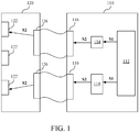
- FIG. 1 is a schematic drawing illustrating a main board 110 and a sub board 120 in the prior art.
- the main board 110 includes a processor 112 , a signal converter 114 and a main board connector 116 .
- the signal converter 114 is connected to the processor 112 and the main board connector 116 .
- the sub board 120 includes a signal output terminal 122 (I/O port) and a sub board connector 126 .
- the signal output terminal 122 is connected to the sub board connector 126 .
- the prior art provides a solution to separate the signal output terminal of the main board 110 from the main board 110 and configure the signal output terminal 122 on the sub board 120 .
- the main board connector 116 of the main board 110 is detachably connected to the sub board connector 126 of the sub board 120 .
- the number and type of the signal output terminals 122 are increased in the manner of replacing the sub board 120 .
- the output signal S2 outputted to the sub board 120 is converted from the native signal S1 outputted by the processor 122 , via the signal converter 114 of the main board 110 , thus the function of the sub board 120 is only to adjust the number and type of the signal output terminal 122 but not the output signal S2 . If the output signals S2 required by the customer is different from the output signal S2 converted by the main board 110 , the main board 110 still needs to be redesigned.
- designing a new main board means complicated procedures such as wiring, write drivers, and verification, which not only requires a lot of development time but also increases the development cost of the customer.
- the present invention provides a functional module board for outputting an output signal to an application terminal, which includes a main board and a sub board.
- the main board includes a processor and a main board connector.
- the processor is connected to the main board connector and outputs a native signal.
- the sub board includes a sub board connector, a signal converter and a signal output terminal.
- the sub board connector is detachably connected to the main board connector for receiving the native signal.
- the signal converter is connected to the sub board connector and the signal output terminal for receiving the native signal, converting the native signal into the output signal according to the application terminal, and outputting the output signal via the signal output terminal.
- the signal output terminal is defined by the application terminal.
- the main board further includes a power slot for inputting a power source.
- the power slot is connected to the processor and the main board connector to drive the processor and provide a standby rail power for the sub board.
- the sub board further includes a power switching component and an external power slot.
- the power switching component is connected to the sub board connector and the signal converter for receiving the standby rail power, and converting the standby rail power into that with different timings according to a power manage signal to be provided to the signal converter.
- the external power slot is configured for connecting to an auxiliary power to provide the power source required by the sub board.
- the power slot of the main board transmits the standby rail power to the sub board connector via the main board connector.
- the pin arrangement for the main board connector and the sub board connector to transmit the standby rail power is power-ground-power.
- the power switching component outputs the voltage with 3.3V, 5V, or 12V by a standby rail power or a main rail power in two different timings according to the requirement of the signal converter.
- the sub board further includes a signal expand component connected to the sub board and the signal converter.
- the signal expand component amplifies the native signal into a plurality of native signals.
- the main board connector has double row of pins; the row of pins near to the processor is configured for transmitting high speed native signal; and the other row of pins is configured for transmitting low speed native signal.
- a plurality of holes are correspondingly configured on the main board and the sub board for connecting the main board connector and the sub board connector to fix the main board and the sub board.
- the functional module board of the present invention outputs the native signal via the processor of the main board, and the native signal is transmitted to the sub board via the connector.
- the signal converter of the sub board converts the native signal to the output signal
- the signal output terminal outputs the output signal to the application terminal.
- the functional module board of the present invention makes the main board have compatibility, and the sub board design can be changed according to different application terminal requirements in the case of the same main board to provide various output signals and various signal output terminals (input/output ports) in different applications. That is to say, when customers need to develop new products, they only need to develop and design the sub board so as to eliminate the time and the cost of developing the main board.
- the present invention not only reduces the developing time of the products but also reduces the developing cost.
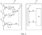
- FIG. 2 is a schematic drawing illustrating a main board and a sub board of the functional module board according to an embodiment of the present invention.
- the functional module board of the present invention includes a main board 210 and a sub board 220 .
- the main board 210 includes a processor 212 , a main board connector 216 and a power slot.
- the processor 212 is connected to the main board connector 216 and the power slot, and the main board connector 216 is connected to the power slot.
- the sub board 220 includes a signal output terminal 222 , a signal converter 224 , a sub board connector 226 , a power switching component, a signal expand component 228 and an external power slot.
- the sub board connector 226 is detachably connected to the main board connector 216 and is connected to the power switching component, the signal converter 224 and the signal expand component 228 .
- the signal converter 224 is connected to the signal output terminal 222 .
- FIG. 3 is a flow chart illustrating the operation of the functional module board according to an embodiment of the present invention.
- the power slot is provided for inserting a power supply for inputting a power to drive the processor 212 , and the power is inputted into the sub board 220 by the main board connector 216 .
- the power slot can be connected to a power management component for converting the DC circuit power inputted by the power supply to the power provided to the processor 212 and to a standby rail power with the voltages of 12V, 5V and 3V provided to the sub board 220 .
- the sub board is in the startup state as the standby rail power is inputted to the component, and there is no special switch required to startup.
- the processor 212 In the step 2000 , the processor 212 generates a native signal S1 after the inputted power drives the processor 212 , and outputs the native signal S1 to the main board connector 216 .
- the native signal S1 includes, but not limited to, a high speed Peripheral Component Interconnect Express (PCIe), a Digital Display Interface (DDI), a Universal Serial Bus (USB), a Low Pin Count Bus (LPC), a Serial Peripheral Interface Bus (SPI), an Inter-IC Sound or Integrated Interchip Sound (I2S), or a System Management Bus (SMBus).
- PCIe Peripheral Component Interconnect Express
- DPI Digital Display Interface
- USB Universal Serial Bus
- LPC Low Pin Count Bus
- SPI Serial Peripheral Interface Bus
- I2S Inter-IC Sound or Integrated Interchip Sound
- SMBBus System Management Bus
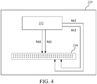
- FIG. 4 is a schematic drawing illustrating the main board connector 216 according to an embodiment of the present invention.
- the main board connector 216 includes 150 pins arranged in an upper row and a lower row.
- the row of pins near the processor 212 side is configured for receiving a high speed native signal S11
- the other row of pins (away from the processor 212 ) is configured for receiving a low speed native signal S12 . Since the high speed native signal S11 needs massive and frequent data transmission, the row of pins near the processor 212 side is selected to transmit the high speed native signal S11 , and the purpose is to enable the high speed native signal S11 to be transmitted to the sub board 220 via the shortest path to avoid signal distortion.
- the low speed native signal S12 has a lower requirement for transmission speed, so it is chosen to match the other row of pins (away from the processor 212 ) to bypass other components during layout routing, and then the circuit configuration of the board becomes more flexible.
- the high speed native signal S11 includes, but not limited to, high speed Peripheral Component Interconnect Express (PCIe) and Digital Display Interface (DDI);
- the low speed native signal S12 includes, but not limited to, Universal Serial Bus (USB), Low Pin Count Bus (LPC), Serial Peripheral Interface Bus (SPI), Inter-IC Sound or Integrated Interchip Sound (I2S) and the like.
- the other feature of the main board connector 216 of the present invention is the pin arrangement of the power source.
- the pin arrangement for the main board connector 216 is POWER-GND-POWER, so that each set of power pins is separated by a set of grounding pins to dissipate the heat generated during transmission of power.
- the main board connector 216 includes a set of power manage signal pins for receiving a power manage signal sent by the processor 212.
- the power manage signal is configured for controlling the timing to convert the standby rail power to the main rail power of the sub board 220.
- the main board connector 216 of the main board 210 transmits the native signal S1 to the sub board connector 226 of the sub board 220 .
- the main board connector 216 and the sub board connector 226 have corresponding pins, and are connected to each other in a board-to-board connector type.
- a plurality of holes are correspondingly configured on the main board 210 and the sub board 220 .
- the copper column can be configured in the holes to fix the relative positions of the main board 210 and the sub board 220 .
- an overlapping area is generated while the main board 210 and the sub board 220 are connected via the main board connector 216 and the sub board connector 226 .
- the lower height components can be configured in the overlapping area, so that the main board 210 and the sub board 220 can be assembled smoothly without interference during the assembling.
- the sub board connector 226 outputs the native signal S1 to the signal converter 224 , and the signal converter 224 converts the native signal S1 to the output signal S2 .
- the signal converter 224 converts the native signal S1 to the output signal S2 according to the application terminal requirements.
- an Audio chip (signal converter 224 ) is configured to convert the Inter-IC Sound or Integrated Interchip Sound (I2S) (native signal S1 ) to the microphone signal (output signal S2 ); and if the application terminal requirement is an image output, a VGA bridge IC (signal converter 224) is configured to convert the Digital Display Interface (DDI) (native signal S1 ) to the VGA Signal (output signal S2 ).
- I2S Inter-IC Sound or Integrated Interchip Sound
- VGA bridge IC (signal converter 224) is configured to convert the Digital Display Interface (DDI) (native signal S1 ) to the VGA Signal (output signal S2 ).
- the power switching component of the sub board 220 receives the standby rail power and the power manage signal from the sub board connector 226 and controls the timing to convert the standby rail power to the main rail power according to the power manage signal. In practical applications, if the power switching component receives the power manage signal, it converts the timing of the standby rail power to that of the main rail power and outputs the main rail power; if the sub board 220 has no requirement of the main rail power according to the sub board 220 applications, the power switching component inputs the standby rail power directly to provide the power. Due to the main board 210 provides the standby rail power with 3.3V, 5V and 12V to the sub board 220 , and the standby rail power can be changed the timing by the power switching component.
- the present invention can provide different powers to different signal converters 224 according to the requirements of the voltage and timing of the signal converter 224 .
- PCIe Peripheral Component Interconnect Express
- DPI Digital Display Interface
- the standby rail power with 3.3V voltage and the main rail power with 5V voltage are required at the same time.
- the power switching component is utilized in the present invention of the sub board 220 to convert the standby rail power to the power sources with specific voltages and timings according to the features of the signal converter 224 , so that the main board 210 only needs to input the power with fixed voltage and the timing, thereby improving the compatibility of the main board 210 .
- the external power slot of the sub board 220 can be configured for receiving an external power to provide extra auxiliary power for the sub board 220 . Therefore, the transmission and amplification of the output signal S2 will not be limited to the power supply.
- the signal converter 224 transmits the output signal S2 to the signal output terminal 222 , and the signal output terminal 222 outputs the output signal S2 to the application terminal.
- the signal output terminal 222 is an input/output port (I/O port), and it can be defined by the requirements of the application terminal. For example, if the application terminal is required to be applied in the high vibration environment such as railways, the signal output terminal 222 can use a lockable connector such as M8 or M12.
- the signal expand component 228 can be connected between the sub board connector 226 and the signal converter 224 for expanding the native signal S1 , and then, a plurality of native signals S1 are converted to the output signals S2 via the signal converter 224 according to the application terminal requirements. For example, if the application terminal requirement is applied in a place with a lot of equipments such as a factory, the native signal S1 is amplified to a plurality of native signals S1 via the signal expand component 228 , and then, the same or different output signals S2 converted respectively by the plurality of native signals S1 are outputted via the signal output terminal 222 according to the factory requirements.
- the signal expand component 228 can be a USB Hub IC or a PCIe Switch IC, but it is not limited thereto.
- some of the native signals S1 outputted by the main board 210 are not necessary to be converted and are outputted to the application terminal via the signal output terminal 222 directly, such as the Universal Serial Bus (USB) signal. Therefore, in some specific application embodiments, the sub board 220 has no need to include the signal converter 224 .
- USB Universal Serial Bus
- the functional module board of the present invention outputs the native signal and the standby rail power by the main board, and the native signal and the standby rail power are transmitted to the sub board via the connector.
- the sub board converts the standby rail power to the required power source of the signal converter, uses the signal converter to convert the native signal to the output signal, and then outputs the output signal to the application terminal via the signal output terminal.
- the functional module board of the present invention makes the main board have compatibility, and the sub board design can be changed according to different requirements of the application terminal in the case of the same main board to provide various output signals and various signal output terminals (input/output ports) in different applications. That is to say, when customers need to develop new products, they only need to develop and design the sub board so as to eliminate the time and the cost of developing the main board.
- the present invention not only reduces the developing time of the products but also reduces the developing cost.
Landscapes
- Engineering & Computer Science (AREA)
- Theoretical Computer Science (AREA)
- General Engineering & Computer Science (AREA)
- Physics & Mathematics (AREA)
- General Physics & Mathematics (AREA)
- Computer Hardware Design (AREA)
- Microelectronics & Electronic Packaging (AREA)
- Power Engineering (AREA)
- Human Computer Interaction (AREA)
- Combinations Of Printed Boards (AREA)
Applications Claiming Priority (1)
| Application Number | Priority Date | Filing Date | Title |
|---|---|---|---|
| TW107118172A TWI663505B (zh) | 2018-05-28 | 2018-05-28 | 功能電路板模組 |
Publications (2)
| Publication Number | Publication Date |
|---|---|
| EP3575918A1 true EP3575918A1 (de) | 2019-12-04 |
| EP3575918B1 EP3575918B1 (de) | 2022-06-29 |
Family
ID=67764236
Family Applications (1)
| Application Number | Title | Priority Date | Filing Date |
|---|---|---|---|
| EP18205288.6A Active EP3575918B1 (de) | 2018-05-28 | 2018-11-08 | Funktionale modulare platine |
Country Status (4)
| Country | Link |
|---|---|
| US (1) | US10635620B2 (de) |
| EP (1) | EP3575918B1 (de) |
| CN (1) | CN110543651B (de) |
| TW (1) | TWI663505B (de) |
Families Citing this family (5)
| Publication number | Priority date | Publication date | Assignee | Title |
|---|---|---|---|---|
| KR102839813B1 (ko) * | 2019-10-10 | 2025-07-28 | 엘지전자 주식회사 | 복수의 인터페이스를 이용하여 다른 전자 장치를 인식하는 방법 및 그 전자 장치 |
| CN114064538A (zh) * | 2021-10-11 | 2022-02-18 | 北京小米移动软件有限公司 | 开发平台 |
| CN113918495A (zh) * | 2021-10-11 | 2022-01-11 | 北京小米移动软件有限公司 | 电源子板 |
| CN113918491A (zh) * | 2021-10-11 | 2022-01-11 | 北京小米移动软件有限公司 | 母板 |
| CN114036095A (zh) * | 2021-10-11 | 2022-02-11 | 北京小米移动软件有限公司 | 转接口 |
Citations (5)
| Publication number | Priority date | Publication date | Assignee | Title |
|---|---|---|---|---|
| US20030226048A1 (en) * | 2002-05-31 | 2003-12-04 | Nguyen Don J. | Method and apparatus for reducing the power consumed by a computer system |
| US20040090761A1 (en) * | 2002-11-12 | 2004-05-13 | Compal Electronics, Inc. | Circuit board assembly with separable first and second circuit board devices |
| US20090031062A1 (en) * | 2007-07-25 | 2009-01-29 | Asustek Computer Inc. | Modularized motherboard |
| US20110019384A1 (en) * | 2009-07-23 | 2011-01-27 | Hon Hai Precision Industry Co., Ltd. | Printed circuit board assembly |
| US20110043989A1 (en) * | 2009-08-18 | 2011-02-24 | Kai-Chen Tien | Motherboard and portable electronic device using the same |
Family Cites Families (17)
| Publication number | Priority date | Publication date | Assignee | Title |
|---|---|---|---|---|
| US7047338B1 (en) * | 2000-07-18 | 2006-05-16 | Igt | Configurable hot-swap communication |
| TWI252401B (en) * | 2003-03-31 | 2006-04-01 | Ricoh Kk | A method and apparatus for controlling connections of PC cards and a passive-card-adapting card used for connecting one of the PC cards to the apparatus |
| TW200737034A (en) * | 2006-03-23 | 2007-10-01 | Micro Star Int Co Ltd | Connector module of graphic card and the device of motherboard thereof |
| US8543751B2 (en) * | 2007-04-30 | 2013-09-24 | Hewlett-Packard Development Company, L.P. | Computer card |
| US20100005211A1 (en) * | 2008-07-02 | 2010-01-07 | Chenbro Micom Co., Ltd. | Adapter board assembly |
| TWI379460B (en) * | 2009-02-27 | 2012-12-11 | Asustek Comp Inc | Circuit board module and connection port collection board |
| TW201039500A (en) * | 2009-04-17 | 2010-11-01 | Asustek Comp Inc | Interface card slot and the circuit board module having the same |
| TW201128370A (en) * | 2010-02-09 | 2011-08-16 | Hon Hai Prec Ind Co Ltd | Motherboard expansion apparatus |
| US8693208B2 (en) * | 2010-08-06 | 2014-04-08 | Ocz Technology Group, Inc. | PCIe bus extension system, method and interfaces therefor |
| US20130238827A1 (en) * | 2012-03-12 | 2013-09-12 | Heng-Sheng Lin | Motherboard having an attached expansion card with both PCI slot and PCIe slot |
| CN103869885A (zh) * | 2012-12-18 | 2014-06-18 | 鸿富锦精密工业(深圳)有限公司 | 扩展卡及支持所述扩展卡的主板 |
| TW201435600A (zh) * | 2013-03-15 | 2014-09-16 | Hon Hai Prec Ind Co Ltd | Tbt晶片集成系統及方法 |
| TW201506633A (zh) * | 2013-08-02 | 2015-02-16 | Good Way Technology Co Ltd | 連接埠配置方法及配置有複數連接埠的組合式電路板模組 |
| TWI598599B (zh) * | 2016-02-19 | 2017-09-11 | 啟碁科技股份有限公司 | 雙電路板組合、電路板與模組化電路板 |
| TWI612749B (zh) * | 2017-05-22 | 2018-01-21 | 富達通科技股份有限公司 | 感應式電源供應器之電路板模組 |
| US10587278B2 (en) * | 2018-02-20 | 2020-03-10 | F.S. Brainard & Company | Sensor to encoder signal converter |
| TWM568993U (zh) * | 2018-05-28 | 2018-10-21 | 凌華科技股份有限公司 | 功能電路板模組 |
-
2018
- 2018-05-28 TW TW107118172A patent/TWI663505B/zh active
- 2018-11-08 EP EP18205288.6A patent/EP3575918B1/de active Active
- 2018-11-09 US US16/186,184 patent/US10635620B2/en active Active
- 2018-11-13 CN CN201811343933.5A patent/CN110543651B/zh active Active
Patent Citations (5)
| Publication number | Priority date | Publication date | Assignee | Title |
|---|---|---|---|---|
| US20030226048A1 (en) * | 2002-05-31 | 2003-12-04 | Nguyen Don J. | Method and apparatus for reducing the power consumed by a computer system |
| US20040090761A1 (en) * | 2002-11-12 | 2004-05-13 | Compal Electronics, Inc. | Circuit board assembly with separable first and second circuit board devices |
| US20090031062A1 (en) * | 2007-07-25 | 2009-01-29 | Asustek Computer Inc. | Modularized motherboard |
| US20110019384A1 (en) * | 2009-07-23 | 2011-01-27 | Hon Hai Precision Industry Co., Ltd. | Printed circuit board assembly |
| US20110043989A1 (en) * | 2009-08-18 | 2011-02-24 | Kai-Chen Tien | Motherboard and portable electronic device using the same |
Also Published As
| Publication number | Publication date |
|---|---|
| US10635620B2 (en) | 2020-04-28 |
| CN110543651B (zh) | 2023-07-25 |
| TWI663505B (zh) | 2019-06-21 |
| TW202004405A (zh) | 2020-01-16 |
| CN110543651A (zh) | 2019-12-06 |
| EP3575918B1 (de) | 2022-06-29 |
| US20190361828A1 (en) | 2019-11-28 |
Similar Documents
| Publication | Publication Date | Title |
|---|---|---|
| US10635620B2 (en) | Functional module board | |
| TWI684869B (zh) | 集線器 | |
| US10002105B2 (en) | Display device | |
| US20100017552A1 (en) | Converter and control system | |
| JP2005346123A (ja) | パラレルインタフェースコネクタを備えたストレージ装置及び同装置に適用される変換コネクタ | |
| US8732345B2 (en) | Image forming apparatus, image processing device, control device, and connection device | |
| US20090031062A1 (en) | Modularized motherboard | |
| US20060104289A1 (en) | Multiplexed computer peripheral connection switching interface | |
| US6894902B2 (en) | Computer expansion device with USB interface | |
| TW202005485A (zh) | 擴充快捷外設互聯標準兼容性的電路 | |
| US20020078281A1 (en) | Portable computer and automatic setting method of master/slave devices for the same | |
| US7266623B2 (en) | Portable computer | |
| CN102882084A (zh) | 硬盘转接装置 | |
| TWM568993U (zh) | 功能電路板模組 | |
| CN115665581A (zh) | 串口隔离模块 | |
| US10712793B2 (en) | External device, electronic device and electronic system | |
| US20210096614A1 (en) | Motherboard and detachable module | |
| CN218920551U (zh) | 串口隔离模块 | |
| US20040205283A1 (en) | Interface module | |
| US20070047537A1 (en) | Expandable structure for peripheral storage device | |
| CN115904306A (zh) | 音频转接装置以及音频转换系统 | |
| CN220121471U (zh) | 一种显示控制电路板及学习机 | |
| CN100377135C (zh) | 双总线适配卡 | |
| CN221239262U (zh) | 一种用于拓展坞的信号转换装置 | |
| CN107608280B (zh) | 多信源usb接口电路 |
Legal Events
| Date | Code | Title | Description |
|---|---|---|---|
| PUAI | Public reference made under article 153(3) epc to a published international application that has entered the european phase |
Free format text: ORIGINAL CODE: 0009012 |
|
| STAA | Information on the status of an ep patent application or granted ep patent |
Free format text: STATUS: THE APPLICATION HAS BEEN PUBLISHED |
|
| AK | Designated contracting states |
Kind code of ref document: A1 Designated state(s): AL AT BE BG CH CY CZ DE DK EE ES FI FR GB GR HR HU IE IS IT LI LT LU LV MC MK MT NL NO PL PT RO RS SE SI SK SM TR |
|
| AX | Request for extension of the european patent |
Extension state: BA ME |
|
| STAA | Information on the status of an ep patent application or granted ep patent |
Free format text: STATUS: REQUEST FOR EXAMINATION WAS MADE |
|
| 17P | Request for examination filed |
Effective date: 20200527 |
|
| RBV | Designated contracting states (corrected) |
Designated state(s): AL AT BE BG CH CY CZ DE DK EE ES FI FR GB GR HR HU IE IS IT LI LT LU LV MC MK MT NL NO PL PT RO RS SE SI SK SM TR |
|
| STAA | Information on the status of an ep patent application or granted ep patent |
Free format text: STATUS: EXAMINATION IS IN PROGRESS |
|
| 17Q | First examination report despatched |
Effective date: 20201106 |
|
| RIC1 | Information provided on ipc code assigned before grant |
Ipc: G06F 13/42 20060101ALI20220324BHEP Ipc: G06F 13/40 20060101ALI20220324BHEP Ipc: G06F 1/26 20060101ALI20220324BHEP Ipc: H05K 1/14 20060101ALI20220324BHEP Ipc: G06F 1/18 20060101AFI20220324BHEP |
|
| GRAP | Despatch of communication of intention to grant a patent |
Free format text: ORIGINAL CODE: EPIDOSNIGR1 |
|
| STAA | Information on the status of an ep patent application or granted ep patent |
Free format text: STATUS: GRANT OF PATENT IS INTENDED |
|
| GRAS | Grant fee paid |
Free format text: ORIGINAL CODE: EPIDOSNIGR3 |
|
| GRAA | (expected) grant |
Free format text: ORIGINAL CODE: 0009210 |
|
| STAA | Information on the status of an ep patent application or granted ep patent |
Free format text: STATUS: THE PATENT HAS BEEN GRANTED |
|
| INTG | Intention to grant announced |
Effective date: 20220503 |
|
| RAP3 | Party data changed (applicant data changed or rights of an application transferred) |
Owner name: ADLINK TECHNOLOGY INC. |
|
| AK | Designated contracting states |
Kind code of ref document: B1 Designated state(s): AL AT BE BG CH CY CZ DE DK EE ES FI FR GB GR HR HU IE IS IT LI LT LU LV MC MK MT NL NO PL PT RO RS SE SI SK SM TR |
|
| REG | Reference to a national code |
Ref country code: CH Ref legal event code: EP |
|
| REG | Reference to a national code |
Ref country code: DE Ref legal event code: R096 Ref document number: 602018037245 Country of ref document: DE |
|
| REG | Reference to a national code |
Ref country code: AT Ref legal event code: REF Ref document number: 1501773 Country of ref document: AT Kind code of ref document: T Effective date: 20220715 |
|
| REG | Reference to a national code |
Ref country code: IE Ref legal event code: FG4D |
|
| REG | Reference to a national code |
Ref country code: SE Ref legal event code: TRGR |
|
| REG | Reference to a national code |
Ref country code: LT Ref legal event code: MG9D |
|
| PG25 | Lapsed in a contracting state [announced via postgrant information from national office to epo] |
Ref country code: NO Free format text: LAPSE BECAUSE OF FAILURE TO SUBMIT A TRANSLATION OF THE DESCRIPTION OR TO PAY THE FEE WITHIN THE PRESCRIBED TIME-LIMIT Effective date: 20220929 Ref country code: LT Free format text: LAPSE BECAUSE OF FAILURE TO SUBMIT A TRANSLATION OF THE DESCRIPTION OR TO PAY THE FEE WITHIN THE PRESCRIBED TIME-LIMIT Effective date: 20220629 Ref country code: HR Free format text: LAPSE BECAUSE OF FAILURE TO SUBMIT A TRANSLATION OF THE DESCRIPTION OR TO PAY THE FEE WITHIN THE PRESCRIBED TIME-LIMIT Effective date: 20220629 Ref country code: GR Free format text: LAPSE BECAUSE OF FAILURE TO SUBMIT A TRANSLATION OF THE DESCRIPTION OR TO PAY THE FEE WITHIN THE PRESCRIBED TIME-LIMIT Effective date: 20220930 Ref country code: FI Free format text: LAPSE BECAUSE OF FAILURE TO SUBMIT A TRANSLATION OF THE DESCRIPTION OR TO PAY THE FEE WITHIN THE PRESCRIBED TIME-LIMIT Effective date: 20220629 Ref country code: BG Free format text: LAPSE BECAUSE OF FAILURE TO SUBMIT A TRANSLATION OF THE DESCRIPTION OR TO PAY THE FEE WITHIN THE PRESCRIBED TIME-LIMIT Effective date: 20220929 |
|
| REG | Reference to a national code |
Ref country code: NL Ref legal event code: MP Effective date: 20220629 |
|
| REG | Reference to a national code |
Ref country code: AT Ref legal event code: MK05 Ref document number: 1501773 Country of ref document: AT Kind code of ref document: T Effective date: 20220629 |
|
| PG25 | Lapsed in a contracting state [announced via postgrant information from national office to epo] |
Ref country code: RS Free format text: LAPSE BECAUSE OF FAILURE TO SUBMIT A TRANSLATION OF THE DESCRIPTION OR TO PAY THE FEE WITHIN THE PRESCRIBED TIME-LIMIT Effective date: 20220629 Ref country code: LV Free format text: LAPSE BECAUSE OF FAILURE TO SUBMIT A TRANSLATION OF THE DESCRIPTION OR TO PAY THE FEE WITHIN THE PRESCRIBED TIME-LIMIT Effective date: 20220629 |
|
| PG25 | Lapsed in a contracting state [announced via postgrant information from national office to epo] |
Ref country code: NL Free format text: LAPSE BECAUSE OF FAILURE TO SUBMIT A TRANSLATION OF THE DESCRIPTION OR TO PAY THE FEE WITHIN THE PRESCRIBED TIME-LIMIT Effective date: 20220629 |
|
| PG25 | Lapsed in a contracting state [announced via postgrant information from national office to epo] |
Ref country code: SM Free format text: LAPSE BECAUSE OF FAILURE TO SUBMIT A TRANSLATION OF THE DESCRIPTION OR TO PAY THE FEE WITHIN THE PRESCRIBED TIME-LIMIT Effective date: 20220629 Ref country code: SK Free format text: LAPSE BECAUSE OF FAILURE TO SUBMIT A TRANSLATION OF THE DESCRIPTION OR TO PAY THE FEE WITHIN THE PRESCRIBED TIME-LIMIT Effective date: 20220629 Ref country code: RO Free format text: LAPSE BECAUSE OF FAILURE TO SUBMIT A TRANSLATION OF THE DESCRIPTION OR TO PAY THE FEE WITHIN THE PRESCRIBED TIME-LIMIT Effective date: 20220629 Ref country code: PT Free format text: LAPSE BECAUSE OF FAILURE TO SUBMIT A TRANSLATION OF THE DESCRIPTION OR TO PAY THE FEE WITHIN THE PRESCRIBED TIME-LIMIT Effective date: 20221031 Ref country code: ES Free format text: LAPSE BECAUSE OF FAILURE TO SUBMIT A TRANSLATION OF THE DESCRIPTION OR TO PAY THE FEE WITHIN THE PRESCRIBED TIME-LIMIT Effective date: 20220629 Ref country code: EE Free format text: LAPSE BECAUSE OF FAILURE TO SUBMIT A TRANSLATION OF THE DESCRIPTION OR TO PAY THE FEE WITHIN THE PRESCRIBED TIME-LIMIT Effective date: 20220629 Ref country code: AT Free format text: LAPSE BECAUSE OF FAILURE TO SUBMIT A TRANSLATION OF THE DESCRIPTION OR TO PAY THE FEE WITHIN THE PRESCRIBED TIME-LIMIT Effective date: 20220629 |
|
| PG25 | Lapsed in a contracting state [announced via postgrant information from national office to epo] |
Ref country code: PL Free format text: LAPSE BECAUSE OF FAILURE TO SUBMIT A TRANSLATION OF THE DESCRIPTION OR TO PAY THE FEE WITHIN THE PRESCRIBED TIME-LIMIT Effective date: 20220629 Ref country code: IS Free format text: LAPSE BECAUSE OF FAILURE TO SUBMIT A TRANSLATION OF THE DESCRIPTION OR TO PAY THE FEE WITHIN THE PRESCRIBED TIME-LIMIT Effective date: 20221029 |
|
| REG | Reference to a national code |
Ref country code: DE Ref legal event code: R097 Ref document number: 602018037245 Country of ref document: DE |
|
| PG25 | Lapsed in a contracting state [announced via postgrant information from national office to epo] |
Ref country code: AL Free format text: LAPSE BECAUSE OF FAILURE TO SUBMIT A TRANSLATION OF THE DESCRIPTION OR TO PAY THE FEE WITHIN THE PRESCRIBED TIME-LIMIT Effective date: 20220629 |
|
| PG25 | Lapsed in a contracting state [announced via postgrant information from national office to epo] |
Ref country code: DK Free format text: LAPSE BECAUSE OF FAILURE TO SUBMIT A TRANSLATION OF THE DESCRIPTION OR TO PAY THE FEE WITHIN THE PRESCRIBED TIME-LIMIT Effective date: 20220629 Ref country code: CZ Free format text: LAPSE BECAUSE OF FAILURE TO SUBMIT A TRANSLATION OF THE DESCRIPTION OR TO PAY THE FEE WITHIN THE PRESCRIBED TIME-LIMIT Effective date: 20220629 |
|
| PLBE | No opposition filed within time limit |
Free format text: ORIGINAL CODE: 0009261 |
|
| STAA | Information on the status of an ep patent application or granted ep patent |
Free format text: STATUS: NO OPPOSITION FILED WITHIN TIME LIMIT |
|
| 26N | No opposition filed |
Effective date: 20230330 |
|
| PG25 | Lapsed in a contracting state [announced via postgrant information from national office to epo] |
Ref country code: MC Free format text: LAPSE BECAUSE OF FAILURE TO SUBMIT A TRANSLATION OF THE DESCRIPTION OR TO PAY THE FEE WITHIN THE PRESCRIBED TIME-LIMIT Effective date: 20220629 |
|
| REG | Reference to a national code |
Ref country code: CH Ref legal event code: PL |
|
| REG | Reference to a national code |
Ref country code: BE Ref legal event code: MM Effective date: 20221130 |
|
| PG25 | Lapsed in a contracting state [announced via postgrant information from national office to epo] |
Ref country code: LI Free format text: LAPSE BECAUSE OF NON-PAYMENT OF DUE FEES Effective date: 20221130 Ref country code: CH Free format text: LAPSE BECAUSE OF NON-PAYMENT OF DUE FEES Effective date: 20221130 |
|
| PG25 | Lapsed in a contracting state [announced via postgrant information from national office to epo] |
Ref country code: SI Free format text: LAPSE BECAUSE OF FAILURE TO SUBMIT A TRANSLATION OF THE DESCRIPTION OR TO PAY THE FEE WITHIN THE PRESCRIBED TIME-LIMIT Effective date: 20220629 Ref country code: LU Free format text: LAPSE BECAUSE OF NON-PAYMENT OF DUE FEES Effective date: 20221108 |
|
| PG25 | Lapsed in a contracting state [announced via postgrant information from national office to epo] |
Ref country code: IE Free format text: LAPSE BECAUSE OF NON-PAYMENT OF DUE FEES Effective date: 20221108 |
|
| PG25 | Lapsed in a contracting state [announced via postgrant information from national office to epo] |
Ref country code: BE Free format text: LAPSE BECAUSE OF NON-PAYMENT OF DUE FEES Effective date: 20221130 |
|
| PG25 | Lapsed in a contracting state [announced via postgrant information from national office to epo] |
Ref country code: IT Free format text: LAPSE BECAUSE OF FAILURE TO SUBMIT A TRANSLATION OF THE DESCRIPTION OR TO PAY THE FEE WITHIN THE PRESCRIBED TIME-LIMIT Effective date: 20220629 |
|
| PG25 | Lapsed in a contracting state [announced via postgrant information from national office to epo] |
Ref country code: HU Free format text: LAPSE BECAUSE OF FAILURE TO SUBMIT A TRANSLATION OF THE DESCRIPTION OR TO PAY THE FEE WITHIN THE PRESCRIBED TIME-LIMIT; INVALID AB INITIO Effective date: 20181108 |
|
| PG25 | Lapsed in a contracting state [announced via postgrant information from national office to epo] |
Ref country code: CY Free format text: LAPSE BECAUSE OF FAILURE TO SUBMIT A TRANSLATION OF THE DESCRIPTION OR TO PAY THE FEE WITHIN THE PRESCRIBED TIME-LIMIT Effective date: 20220629 |
|
| PG25 | Lapsed in a contracting state [announced via postgrant information from national office to epo] |
Ref country code: MK Free format text: LAPSE BECAUSE OF FAILURE TO SUBMIT A TRANSLATION OF THE DESCRIPTION OR TO PAY THE FEE WITHIN THE PRESCRIBED TIME-LIMIT Effective date: 20220629 |
|
| PG25 | Lapsed in a contracting state [announced via postgrant information from national office to epo] |
Ref country code: TR Free format text: LAPSE BECAUSE OF FAILURE TO SUBMIT A TRANSLATION OF THE DESCRIPTION OR TO PAY THE FEE WITHIN THE PRESCRIBED TIME-LIMIT Effective date: 20220629 |
|
| PG25 | Lapsed in a contracting state [announced via postgrant information from national office to epo] |
Ref country code: MT Free format text: LAPSE BECAUSE OF FAILURE TO SUBMIT A TRANSLATION OF THE DESCRIPTION OR TO PAY THE FEE WITHIN THE PRESCRIBED TIME-LIMIT Effective date: 20220629 |
|
| PG25 | Lapsed in a contracting state [announced via postgrant information from national office to epo] |
Ref country code: BG Free format text: LAPSE BECAUSE OF FAILURE TO SUBMIT A TRANSLATION OF THE DESCRIPTION OR TO PAY THE FEE WITHIN THE PRESCRIBED TIME-LIMIT Effective date: 20220629 |
|
| PG25 | Lapsed in a contracting state [announced via postgrant information from national office to epo] |
Ref country code: BG Free format text: LAPSE BECAUSE OF FAILURE TO SUBMIT A TRANSLATION OF THE DESCRIPTION OR TO PAY THE FEE WITHIN THE PRESCRIBED TIME-LIMIT Effective date: 20220629 |
|
| PGFP | Annual fee paid to national office [announced via postgrant information from national office to epo] |
Ref country code: GB Payment date: 20250902 Year of fee payment: 8 |
|
| PGFP | Annual fee paid to national office [announced via postgrant information from national office to epo] |
Ref country code: FR Payment date: 20250902 Year of fee payment: 8 |
|
| PGFP | Annual fee paid to national office [announced via postgrant information from national office to epo] |
Ref country code: SE Payment date: 20250902 Year of fee payment: 8 |
|
| PGFP | Annual fee paid to national office [announced via postgrant information from national office to epo] |
Ref country code: DE Payment date: 20250903 Year of fee payment: 8 |