EP3574519B1 - Support for a semiconductor structure - Google Patents
Support for a semiconductor structure Download PDFInfo
- Publication number
- EP3574519B1 EP3574519B1 EP18700172.2A EP18700172A EP3574519B1 EP 3574519 B1 EP3574519 B1 EP 3574519B1 EP 18700172 A EP18700172 A EP 18700172A EP 3574519 B1 EP3574519 B1 EP 3574519B1
- Authority
- EP
- European Patent Office
- Prior art keywords
- support
- layer
- insulating layer
- trapping layer
- ohm
- Prior art date
- Legal status (The legal status is an assumption and is not a legal conclusion. Google has not performed a legal analysis and makes no representation as to the accuracy of the status listed.)
- Active
Links
- 239000004065 semiconductor Substances 0.000 title claims description 22
- 239000000758 substrate Substances 0.000 claims description 59
- VYPSYNLAJGMNEJ-UHFFFAOYSA-N Silicium dioxide Chemical compound O=[Si]=O VYPSYNLAJGMNEJ-UHFFFAOYSA-N 0.000 claims description 25
- 229910021420 polycrystalline silicon Inorganic materials 0.000 claims description 16
- 235000012239 silicon dioxide Nutrition 0.000 claims description 12
- 239000000377 silicon dioxide Substances 0.000 claims description 9
- OKTJSMMVPCPJKN-UHFFFAOYSA-N Carbon Chemical compound [C] OKTJSMMVPCPJKN-UHFFFAOYSA-N 0.000 claims description 5
- XUIMIQQOPSSXEZ-UHFFFAOYSA-N Silicon Chemical compound [Si] XUIMIQQOPSSXEZ-UHFFFAOYSA-N 0.000 claims description 5
- 229910052799 carbon Inorganic materials 0.000 claims description 5
- 229910052710 silicon Inorganic materials 0.000 claims description 5
- 239000010703 silicon Substances 0.000 claims description 5
- 229910021417 amorphous silicon Inorganic materials 0.000 claims description 3
- 239000011521 glass Substances 0.000 claims description 3
- 229910021426 porous silicon Inorganic materials 0.000 claims description 3
- 239000010453 quartz Substances 0.000 claims description 3
- 229910052594 sapphire Inorganic materials 0.000 claims description 3
- 239000010980 sapphire Substances 0.000 claims description 3
- 238000010438 heat treatment Methods 0.000 description 12
- 239000000463 material Substances 0.000 description 11
- 238000005259 measurement Methods 0.000 description 10
- 230000005672 electromagnetic field Effects 0.000 description 9
- 230000015572 biosynthetic process Effects 0.000 description 7
- 239000002800 charge carrier Substances 0.000 description 6
- 230000008878 coupling Effects 0.000 description 6
- 238000010168 coupling process Methods 0.000 description 6
- 238000005859 coupling reaction Methods 0.000 description 6
- 230000007423 decrease Effects 0.000 description 5
- 230000000694 effects Effects 0.000 description 5
- 238000004519 manufacturing process Methods 0.000 description 5
- 230000003647 oxidation Effects 0.000 description 4
- 238000007254 oxidation reaction Methods 0.000 description 4
- 238000012545 processing Methods 0.000 description 4
- 229910052814 silicon oxide Inorganic materials 0.000 description 4
- 229910052581 Si3N4 Inorganic materials 0.000 description 3
- 230000008901 benefit Effects 0.000 description 3
- 238000012512 characterization method Methods 0.000 description 3
- 230000000295 complement effect Effects 0.000 description 3
- 230000003247 decreasing effect Effects 0.000 description 3
- 238000000151 deposition Methods 0.000 description 3
- 230000008021 deposition Effects 0.000 description 3
- 239000012212 insulator Substances 0.000 description 3
- 230000003993 interaction Effects 0.000 description 3
- 230000000149 penetrating effect Effects 0.000 description 3
- 238000001953 recrystallisation Methods 0.000 description 3
- 238000000663 remote plasma-enhanced chemical vapour deposition Methods 0.000 description 3
- HQVNEWCFYHHQES-UHFFFAOYSA-N silicon nitride Chemical compound N12[Si]34N5[Si]62N3[Si]51N64 HQVNEWCFYHHQES-UHFFFAOYSA-N 0.000 description 3
- 238000004088 simulation Methods 0.000 description 3
- 238000005728 strengthening Methods 0.000 description 3
- 230000007847 structural defect Effects 0.000 description 3
- IJGRMHOSHXDMSA-UHFFFAOYSA-N Atomic nitrogen Chemical compound N#N IJGRMHOSHXDMSA-UHFFFAOYSA-N 0.000 description 2
- 238000004090 dissolution Methods 0.000 description 2
- 239000002019 doping agent Substances 0.000 description 2
- 238000004518 low pressure chemical vapour deposition Methods 0.000 description 2
- 238000000034 method Methods 0.000 description 2
- 230000035515 penetration Effects 0.000 description 2
- 238000005334 plasma enhanced chemical vapour deposition Methods 0.000 description 2
- 238000000623 plasma-assisted chemical vapour deposition Methods 0.000 description 2
- 238000005498 polishing Methods 0.000 description 2
- 239000011148 porous material Substances 0.000 description 2
- 230000001902 propagating effect Effects 0.000 description 2
- 239000000126 substance Substances 0.000 description 2
- WSMQKESQZFQMFW-UHFFFAOYSA-N 5-methyl-pyrazole-3-carboxylic acid Chemical compound CC1=CC(C(O)=O)=NN1 WSMQKESQZFQMFW-UHFFFAOYSA-N 0.000 description 1
- 238000009825 accumulation Methods 0.000 description 1
- 230000004913 activation Effects 0.000 description 1
- QVGXLLKOCUKJST-UHFFFAOYSA-N atomic oxygen Chemical compound [O] QVGXLLKOCUKJST-UHFFFAOYSA-N 0.000 description 1
- 230000001419 dependent effect Effects 0.000 description 1
- 238000005516 engineering process Methods 0.000 description 1
- 230000001747 exhibiting effect Effects 0.000 description 1
- 238000002474 experimental method Methods 0.000 description 1
- 230000006872 improvement Effects 0.000 description 1
- 230000010354 integration Effects 0.000 description 1
- 229910021421 monocrystalline silicon Inorganic materials 0.000 description 1
- 229910052757 nitrogen Inorganic materials 0.000 description 1
- 229910052760 oxygen Inorganic materials 0.000 description 1
- 239000001301 oxygen Substances 0.000 description 1
- 230000008569 process Effects 0.000 description 1
- HBMJWWWQQXIZIP-UHFFFAOYSA-N silicon carbide Chemical compound [Si+]#[C-] HBMJWWWQQXIZIP-UHFFFAOYSA-N 0.000 description 1
- 229910010271 silicon carbide Inorganic materials 0.000 description 1
- 239000002210 silicon-based material Substances 0.000 description 1
- 229910021483 silicon-carbon alloy Inorganic materials 0.000 description 1
- 238000012546 transfer Methods 0.000 description 1
- 238000003949 trap density measurement Methods 0.000 description 1
Images

Classifications
-
- H—ELECTRICITY
- H01—ELECTRIC ELEMENTS
- H01L—SEMICONDUCTOR DEVICES NOT COVERED BY CLASS H10
- H01L21/00—Processes or apparatus adapted for the manufacture or treatment of semiconductor or solid state devices or of parts thereof
- H01L21/02—Manufacture or treatment of semiconductor devices or of parts thereof
- H01L21/02002—Preparing wafers
-
- H—ELECTRICITY
- H01—ELECTRIC ELEMENTS
- H01L—SEMICONDUCTOR DEVICES NOT COVERED BY CLASS H10
- H01L21/00—Processes or apparatus adapted for the manufacture or treatment of semiconductor or solid state devices or of parts thereof
- H01L21/02—Manufacture or treatment of semiconductor devices or of parts thereof
- H01L21/04—Manufacture or treatment of semiconductor devices or of parts thereof the devices having at least one potential-jump barrier or surface barrier, e.g. PN junction, depletion layer or carrier concentration layer
- H01L21/18—Manufacture or treatment of semiconductor devices or of parts thereof the devices having at least one potential-jump barrier or surface barrier, e.g. PN junction, depletion layer or carrier concentration layer the devices having semiconductor bodies comprising elements of Group IV of the Periodic System or AIIIBV compounds with or without impurities, e.g. doping materials
- H01L21/30—Treatment of semiconductor bodies using processes or apparatus not provided for in groups H01L21/20 - H01L21/26
- H01L21/31—Treatment of semiconductor bodies using processes or apparatus not provided for in groups H01L21/20 - H01L21/26 to form insulating layers thereon, e.g. for masking or by using photolithographic techniques; After treatment of these layers; Selection of materials for these layers
- H01L21/3205—Deposition of non-insulating-, e.g. conductive- or resistive-, layers on insulating layers; After-treatment of these layers
- H01L21/321—After treatment
- H01L21/3215—Doping the layers
- H01L21/32155—Doping polycristalline - or amorphous silicon layers
-
- H—ELECTRICITY
- H01—ELECTRIC ELEMENTS
- H01L—SEMICONDUCTOR DEVICES NOT COVERED BY CLASS H10
- H01L21/00—Processes or apparatus adapted for the manufacture or treatment of semiconductor or solid state devices or of parts thereof
- H01L21/70—Manufacture or treatment of devices consisting of a plurality of solid state components formed in or on a common substrate or of parts thereof; Manufacture of integrated circuit devices or of parts thereof
- H01L21/71—Manufacture of specific parts of devices defined in group H01L21/70
- H01L21/76—Making of isolation regions between components
- H01L21/762—Dielectric regions, e.g. EPIC dielectric isolation, LOCOS; Trench refilling techniques, SOI technology, use of channel stoppers
- H01L21/7624—Dielectric regions, e.g. EPIC dielectric isolation, LOCOS; Trench refilling techniques, SOI technology, use of channel stoppers using semiconductor on insulator [SOI] technology
- H01L21/76251—Dielectric regions, e.g. EPIC dielectric isolation, LOCOS; Trench refilling techniques, SOI technology, use of channel stoppers using semiconductor on insulator [SOI] technology using bonding techniques
- H01L21/76254—Dielectric regions, e.g. EPIC dielectric isolation, LOCOS; Trench refilling techniques, SOI technology, use of channel stoppers using semiconductor on insulator [SOI] technology using bonding techniques with separation/delamination along an ion implanted layer, e.g. Smart-cut, Unibond
Definitions
- the present invention relates to a support for a semiconductor structure.
- Integrated devices are usually formed on substrates that mainly serve to hold them during their fabrication.
- the increase in the degree of integration and the expected performance of these devices has led to an increasingly tighter coupling of their performance and the properties of the substrate on which they are formed.
- This is particularly the case for RF devices processing signals the frequency of which is comprised between about 3 kHz and 300 GHz, which are in particular employed in the telecommunications field (telephony, Wi-Fi, Bluetooth, etc.).
- the electromagnetic fields generated by high-frequency signals propagating through the integrated devices penetrate into the bulk of the substrate and interact with any charge carriers found there. This leads to coupling losses that consume some of the power of the signal and possibly to crosstalk between components.
- substrate charge carriers may generate undesired harmonics, which may interfere with the signals propagating through the integrated devices and degrade device quality.
- the substrate employed comprises a buried insulating layer between a support and a useful layer on and in which the integrated devices are formed.
- Charges trapped in the insulating layer lead charges of complementary sign to accumulate under this insulating layer, forming a conductive plane in the support. In this conductive plane, mobile charges are liable to interact strongly with the electromagnetic fields generated by the components of the useful layer.
- a charge trapping layer for example a layer of 1 to 5 microns of polycrystalline silicon.
- the boundaries of the grains forming the polycrystal then form charge traps, the trapped charge carriers possibly originating from the trapping layer itself or from the subjacent support.
- the formation of the conductive plane under the insulating layer is prevented.
- the fabrication of this type of substrate is for example described in documents FR2860341 , FR2933233 , FR2953640 , US2015115480 , US7268060 , US6544656 or WO 2016 / 140 850 .
- the device/substrate coupling remains dependent on the strength of the interaction between the electromagnetic fields and the mobile charges in the support, and hence on the depth of penetration of these fields into this support.
- the density and/or mobility of these charges depends on the resistivity of the support.
- a trapping layer of 1 to 5 microns in thickness may be suitable for limiting device/substrate coupling, even when the electromagnetic field penetrates deeply into the support. The integrity of the signals, and hence the radiofrequency (RF) performance of the devices integrated into the useful layer, is thus preserved.
- RF radiofrequency
- document US9129800 envisages forming a silicon oxide layer between the crystalline support and the charge trapping layer.
- this layer must necessarily have an initial thickness, before application of the heat treatments, that is relatively low, between 0.5 and 10 nm, in order to have a final thickness, after application of the heat treatments, that is lower than 2 nm.
- this layer must be chosen according to the thermal budget to which the substrate will be subjected so as not to negatively affect its RF performance.
- the trapping layer When the insulating layer is absent for the entire duration of the heat treatment, the trapping layer is liable to recrystallize, either partially or completely. Consequently, the lower grain boundary density or the large size of these grains decreases the trapping properties of the layer.
- the insulating oxide layer When the final thickness of the insulating oxide layer is higher than 2 nm, it is not transparent to the charges present in the support. These charges are therefore able to pass through the insulating layer only by tunnel effect, and are not able to diffuse into the polycrystalline layer and to be trapped therein. These charges thus accumulate in the support and a conductive plane forms under the insulating layer, which has a negative effect on the RF performance of the substrate.
- the heat treatments to which a substrate may be subjected are not always known in advance of its fabrication, in particular those which are applied during the formation of an integrated device.
- these heat treatments may affect the quality or the thickness of this silicon dioxide insulating layer, for example by dissolution.
- the heat treatments in device fabrication can have high thermal budgets, which may have a significant effect on the quality of the trapping layer in the event that the oxide layer has not been chosen with a suitable thickness. This may thus be a thermal processing operation at 1200°C for several minutes as is the case when it is for the purpose of introducing strain into zones of the useful layer using a buried oxide creep technique or during thermal processing operations for dopant activation.
- the present invention aims to overcome all or some of the aforementioned drawbacks.
- one subject of the invention provides, within its widest accepted form, a support for a semiconductor structure or a surface or bulk acoustic wave type device comprising:
- the first insulating layer allows a thick trapping layer to be formed, this trapping layer exhibiting excellent charge trapping properties and having a low likelihood of recrystallizing.
- this insulating layer exhibiting excellent charge trapping properties and having a low likelihood of recrystallizing.
- the inventors of the present application have observed that the decrease in RF performance that could be caused by this insulating layer was largely compensated for by the benefits brought by the thick trapping layer, the formation of which it made possible.
- the subject of the invention provides a semiconductor structure or a surface or bulk acoustic wave type device comprising:
- Figure 1 schematically shows a support 1 for a semiconductor structure according to the invention.
- the support 1 may take the form of a circular wafer of standardized size, for example of 200 mm or 300 mm or even 450 mm in diameter.
- the invention is in no way limited to these dimensions or to this shape.
- the support 1 will take the form of a block of material of rectangular or square longitudinal cross section the dimensions of which, from a few millimetres to a few centimetres, correspond to the dimensions of the integrated device.
- the support 1 comprises a base substrate 3, which is typically a few hundred microns in thickness.
- the base substrate has a high resistivity, higher than 1000 ohm.centimetre, and even more preferably higher than 3000 ohm.centimetre.
- the density of charges, i.e. holes or electrons, that are liable to move in the base substrate is thus limited.
- the invention is not limited to a base substrate having such a resistivity, and it also provides advantages in terms of RF performance when the base substrate has a more usual resistivity, of about a few hundred ohm.centimetres, for example lower than 1000 ohm.cm, or than 500 ohm.cm or than 10 ohm.cm.
- the base substrate 3 is preferably made of monocrystalline silicon. It may for example be a CZ substrate containing a small amount of interstitial oxygen, this type of substrate, as is well known per se, having a resistivity that may be higher than 1000 ohm.centimetre.
- the base substrate may alternatively be formed from another material: it may for example be made of sapphire, of glass, of quartz, of silicon carbide, etc.
- the support 1 also includes, positioned on and making direct contact with the base substrate 3, a first silicon dioxide insulating layer 2a.
- the first insulating layer 2a has a thickness greater than 20 nm, for example comprised between 20 nm and 20 microns. It may be obtained by oxidation of the base substrate 3 or by deposition on this substrate. In order to limit the time and cost required to form the first insulating layer, its thickness may be chosen so that it is comprised between 100 and 200 nm, such as for example 145 nm.
- the first insulating layer is stable with temperature, even for high thermal budgets. It may in particular be exposed to temperatures higher than or equal to 1200°C for a duration of several hours without breaking down, for example by dissolution.
- the support 1 also includes, positioned on and making direct contact with the first insulating layer 2a, a trapping layer 2.
- the trapping layer 2 has a resistivity higher than 1000 ohm.cm, preferably higher than 10 kohm.cm.
- the function of the trapping layer is to trap any charge carriers present in the support 1 and to limit their mobility. This is especially the case when the support 1 is provided with a semiconductor structure that emits an electromagnetic field that penetrates into the support and that is therefore liable to interact with these charges and to make them mobile.
- the trapping layer 2 may, in general, be formed from a non-crystalline semiconductor layer having structural defects such as dislocations, grain boundaries, amorphous zones, interstices, inclusions, pores, etc.
- the structural defects form traps for any charges flowing through the material, for example at the site of incomplete or dangling chemical bonds. Conduction is thus prevented in the trapping layer, which consequently exhibits high resistivity. Since the trapping layer does not make direct contact with the support but with the amorphous insulating layer, the trapping properties of this layer may be conserved even when the support undergoes a very high heat treatment. The structural defects are unlikely to undergo recrystallization.
- the trapping layer 2 is preferably made of polycrystallinesilicon. However, it may be formed from or comprise another polycrystalline semiconductor material. Alternatively, the trapping layer 2 may be formed from or comprise amorphous or porous silicon.
- the trapping layer 2 is also possible to envisage inserting at least one intermediate layer into the trapping layer 2, for example a carbon layer or a layer composed of a carbon-silicon alloy.
- the intermediate layer may also comprise, or be formed from, silicon oxide or silicon nitride.
- the trapping layer 2 is then formed from alternating layers of polycrystalline silicon (or of another material, or of an amorphous or porous material) and intermediate layers of a different nature (of silicon dioxide or nitride, of carbon, etc.).
- the trapping layer 2 has a high resistivity higher than 1000 ohm.centimetre. To this end, the trapping layer 2 is not intentionally doped, i.e. it has a charge carrier dopant concentration lower than 10 E14 atoms per cubic centimetre. It may be rich in nitrogen or in carbon in order to improve its resistivity characteristic.
- the fabrication of the trapping layer 2 on the base substrate 3 provided with the first insulating layer 2a is particularly straightforward and achievable using industry-standard deposition equipment. It may thus involve RPCVD (remote plasma-enhanced chemical vapour deposition) or PECVD (plasma-enhanced chemical vapour deposition). It may also involve LPCVD (low-pressure chemical vapour deposition).
- RPCVD remote plasma-enhanced chemical vapour deposition
- PECVD plasma-enhanced chemical vapour deposition
- LPCVD low-pressure chemical vapour deposition
- a trapping layer 2 based on polycrystalline silicon produced on the first insulating layer 2a and having a thickness greater than 20 nm was formed from grains the dimensions of which, typically comprised between 10 and 900 nm, were particularly suitable for effective charge trapping. Moreover, the dimensions of these grains are relatively constant throughout the thickness of the trapping layer 2, even when the thickness of the latter is substantial. These properties are also conserved after the trapping layer 2 has been exposed to a thermal budget, even to a high thermal budget.
- grain size directly affects the RF performance of the support in two ways. Firstly, larger grains lead to a lower density of grain boundaries in the material. Since these boundaries form a prime zone of charge trapping, trap density is decreased.
- the grains also form a confining space for the charge carriers that reside therein.
- the charges behave, as seen by the device, as in a defect-free material.
- the size of the grains must preferably be comprised between 100 nm (below which their thermal stability is no longer ensured and hence there is a risk that they will recrystallize with temperature) and 1000 nm (above which the RF performance of the support is affected).
- a support 1 according to the invention may therefore have a thick trapping layer 2, having a thickness greater than 5 microns, and potentially reaching 10 microns or 20 microns, comprising a polycrystalline silicon material formed from grains the size of which is comprised between 10 and 900 nm.
- a thick trapping layer 2 having a thickness greater than 5 microns, and potentially reaching 10 microns or 20 microns, comprising a polycrystalline silicon material formed from grains the size of which is comprised between 10 and 900 nm.
- the cited prior art document recommends against placing a thick first insulating layer 2a between the trapping layer 2 and the base substrate 3, as recommended by the present invention.
- the presence of charges in this insulator leads to the formation of a conductive plane consisting of charges of complementary sign in the base substrate 3, under the first insulating layer 2a. This conductive plane affects the radiofrequency performance of the support 1.
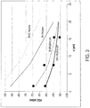
- the graph of Figure 3 presents the results of a series of experiments and simulations prepared by the applicant.
- a plurality of supports having different characteristics and in accordance with the invention have been prepared. These supports comprise a base substrate consisting of a silicon wafer having a diameter of 300 mm and a resistivity of 17,6 k.ohms .
- the base substrates have each been provided with a silicon dioxide insulating layer having a thickness of 145 nm by thermal oxidation.
- a trapping layer made of polycrystalline silicon has been formed on this insulating layer by RPCVD, this layer having a thickness of 2 microns, 7 microns, and 16 microns.
- a characterization measurement referred to as a second harmonic distortion measurement, has then been performed on each of the supports prepared in this way. This measurement is made at 900 MHz. To this end, a silicon dioxide layer and coplanar metallic lines have been formed on each support.
- the axis of the abscissae of the graph of Figure 3 represents the thickness "e" of the trapping layer 2, in microns.
- the axis of the ordinates represents the second harmonic distortion measurement (denoted by HD2) in dBm.
- the six measurements made have been represented by points on the graph of Figure 3 . These measurement points have made it possible to calibrate a simulation of the second harmonic distortion measurement for a support having a base substrate of determined resistivity and having a polycrystalline silicon trapping layer of determined thickness.
- the simulation measurements are represented on the graph of Figure 3 by solid lines for various resistivity values of the base substrate.
- the RF performance of all of the supports is improved when the thickness of the polycrystalline silicon layer increases. More specifically, performance is notably increased when the thickness of the trapping layer is greater than 5 microns.
- the presence of the insulating layer does not limit the level of performance that may be reached. These levels of performances are expected to be stable regardless of the temperature to which the support could be exposed, since the insulating layer prevents the recrystallization of the polycrystalline trapping layer.
- this second insulating layer 4 may be formed by deposition or by oxidation of the trapping layer 2. Provision may be made for a polishing step before and/or after the formation of the second insulating layer 4, in order to improve the quality of this assembly.
- the support 1 is intended to receive a semiconductor structure on the side of the trapping layer 2.
- This structure may be formed in multiple ways on the support 1, but advantageously this formation comprises a step of transferring a useful layer 5 to the support.
- this transfer is usually achieved by bonding the face of a donor substrate to the support 1.
- the latter may or may not be provided with the insulating layer 4.
- the donor substrate may have been provided beforehand with another insulating layer 6 of the same nature or of a different nature to the second insulating layer 4. It may for example be a silicon oxide or silicon nitride.
- the assembly may undergo a strengthening heat treatment, even one having a high thermal budget, since the trapping layer 2 of the support is not liable to recrystallize by virtue of the presence of the insulating layer 2a.
- the strengthening heat treatment may correspond to thermal processing for several hours at 1200°C, which is generally required for fully strengthening a bond bringing two silicon oxide layers into contact.
- the thickness of the donor substrate is decreased to form the useful layer 5.
- This decreasing step may be a step of mechanical or chemical thinning. It may also be a fracture level with a fragile zone introduced beforehand into the donor substrate, for example according to the principles of the Smart CutTM technology.
- a sequence of steps for finishing the useful layer 5, such as a polishing step, a heat treatment under a reducing or inert atmosphere, and a sacrificial oxidation may be carried out after the thickness-decreasing step.
- the donor substrate is a simple semiconductor substrate, i.e. one that comprises no integrated devices
- a semiconductor-on-insulator substrate is thus formed, in which, as is shown in Figure 3 , the useful layer 5 is a virgin semiconductor layer comprising the support of the invention.
- the substrate may then be used to form integrated devices.
- semiconductor structure irrespectively refers to an integrated device whether the latter be formed from semiconductor materials or not.
- semiconductor structure may be a surface or bulk acoustic wave type device, typically produced on and in a layer made of piezoelectric material, such as lithium tantalate.
- semiconductor structure also refers to a layer (or a plurality of layers) of virgin device material, whether based on semiconductor materials or not, and in which integrated devices may be formed.
Description
- The present invention relates to a support for a semiconductor structure.
- Integrated devices are usually formed on substrates that mainly serve to hold them during their fabrication. However, the increase in the degree of integration and the expected performance of these devices has led to an increasingly tighter coupling of their performance and the properties of the substrate on which they are formed. This is particularly the case for RF devices processing signals the frequency of which is comprised between about 3 kHz and 300 GHz, which are in particular employed in the telecommunications field (telephony, Wi-Fi, Bluetooth, etc.).
- By way of example of device/substrate coupling, the electromagnetic fields generated by high-frequency signals propagating through the integrated devices penetrate into the bulk of the substrate and interact with any charge carriers found there. This leads to coupling losses that consume some of the power of the signal and possibly to crosstalk between components.
- According to a second example of coupling, substrate charge carriers may generate undesired harmonics, which may interfere with the signals propagating through the integrated devices and degrade device quality.
- These effects are especially observable when the substrate employed comprises a buried insulating layer between a support and a useful layer on and in which the integrated devices are formed. Charges trapped in the insulating layer lead charges of complementary sign to accumulate under this insulating layer, forming a conductive plane in the support. In this conductive plane, mobile charges are liable to interact strongly with the electromagnetic fields generated by the components of the useful layer.
- To prevent or limit this effect, it is known to insert, between the buried insulating layer and the support, directly under the insulating layer, a charge trapping layer, for example a layer of 1 to 5 microns of polycrystalline silicon. The boundaries of the grains forming the polycrystal then form charge traps, the trapped charge carriers possibly originating from the trapping layer itself or from the subjacent support. Thus, the formation of the conductive plane under the insulating layer is prevented. The fabrication of this type of substrate is for example described in documents
FR2860341 FR2933233 FR2953640 US2015115480 ,US7268060 ,US6544656 orWO 2016 / 140 850 . - In the presence of a trapping layer, the device/substrate coupling remains dependent on the strength of the interaction between the electromagnetic fields and the mobile charges in the support, and hence on the depth of penetration of these fields into this support. The density and/or mobility of these charges depends on the resistivity of the support.
- When the resistivity of the support is relatively high (and therefore charge density relatively low), higher than 1000 ohm.cm, a trapping layer of 1 to 5 microns in thickness may be suitable for limiting device/substrate coupling, even when the electromagnetic field penetrates deeply into the support. The integrity of the signals, and hence the radiofrequency (RF) performance of the devices integrated into the useful layer, is thus preserved.
- In contrast, when the resistivity of the support is lower, lower than 1000 ohm.cm, or when the performance expected from the integrated device is high, it would be desirable to be able to form a very thick trapping layer, of greater than 5 microns, or even than 10 or 20 microns, in thickness, in order to shift the zone in which the charges are mobile deeper into the substrate and to limit the depth of penetration of the electromagnetic fields into this support. Interactions with these electromagnetic fields could thus be prevented and the performance of devices integrated into the useful layer improved.
- However, it has been observed that increasing the thickness of a trapping layer beyond 5 microns does not always lead to the expected improvement in performance, in particular because this layer is liable to recrystallize during the heat treatments that it is liable to undergo. These heat treatments may correspond to those required to produce the substrate itself or to those required to fabricate an RF integrated device in or on the useful layer of the substrate.
- In order to prevent the recrystallization of this layer, document
US9129800 - According to this document, this layer must necessarily have an initial thickness, before application of the heat treatments, that is relatively low, between 0.5 and 10 nm, in order to have a final thickness, after application of the heat treatments, that is lower than 2 nm.
- Stated otherwise, the initial thickness of this layer must be chosen according to the thermal budget to which the substrate will be subjected so as not to negatively affect its RF performance.
- When the insulating layer is absent for the entire duration of the heat treatment, the trapping layer is liable to recrystallize, either partially or completely. Consequently, the lower grain boundary density or the large size of these grains decreases the trapping properties of the layer.
- When the final thickness of the insulating oxide layer is higher than 2 nm, it is not transparent to the charges present in the support. These charges are therefore able to pass through the insulating layer only by tunnel effect, and are not able to diffuse into the polycrystalline layer and to be trapped therein. These charges thus accumulate in the support and a conductive plane forms under the insulating layer, which has a negative effect on the RF performance of the substrate.
- Choosing a suitable initial thickness for this oxide is not straightforward. Specifically, the heat treatments to which a substrate may be subjected are not always known in advance of its fabrication, in particular those which are applied during the formation of an integrated device. However, these heat treatments may affect the quality or the thickness of this silicon dioxide insulating layer, for example by dissolution. In this regard, it has been observed that the heat treatments in device fabrication can have high thermal budgets, which may have a significant effect on the quality of the trapping layer in the event that the oxide layer has not been chosen with a suitable thickness. This may thus be a thermal processing operation at 1200°C for several minutes as is the case when it is for the purpose of introducing strain into zones of the useful layer using a buried oxide creep technique or during thermal processing operations for dopant activation.
- The teaching of the cited prior art document is therefore not straightforward to implement without having knowledge of the total thermal budget that the trapping layer will receive over the course of all of the steps of fabricating the substrate and the integrated devices that are to be formed on this substrate.
- The present invention aims to overcome all or some of the aforementioned drawbacks.
- With a view to achieving this aim, one subject of the invention provides, within its widest accepted form, a support for a semiconductor structure or a surface or bulk acoustic wave type device comprising:
- a base substrate;
- a first silicon dioxide insulating layer positioned on the base substrate and having a thickness greater than 20 nm;
- a charge trapping layer having a resistivity higher than 1000 ohm.cm and a thickness greater than 5 microns positioned on the first insulating layer.
- The first insulating layer allows a thick trapping layer to be formed, this trapping layer exhibiting excellent charge trapping properties and having a low likelihood of recrystallizing. Unexpectedly, the inventors of the present application have observed that the decrease in RF performance that could be caused by this insulating layer was largely compensated for by the benefits brought by the thick trapping layer, the formation of which it made possible.
- According to other advantageous and non-limiting features of the invention, which may be implemented alone or in any technically feasible combination:
- the trapping layer comprises polycrystalline silicon;
- the polycrystalline silicon is rich in carbon;
- the polycrystalline silicon consists of silicon grains having dimensions comprised between 10 nm and 900 nm;
- the trapping layer comprises amorphous or porous silicon;
- the trapping layer has a thickness greater than 10 microns;
- the trapping layer is formed from alternating layers of polycrystalline silicon and silicon dioxide;
- the base substrate has a resistivity lower than 1000 ohm.cm or than 500 ohm.cm or than 10 ohm.cm;
- the base substrate has a resistivity higher than 1000 ohm.cm or than 10k ohm.cm;
- the base substrate is made of silicon, of quartz, of glass or of sapphire;
- the support comprises a second insulating layer positioned on the trapping layer.
- According to another aspect, the subject of the invention provides a semiconductor structure or a surface or bulk acoustic wave type device comprising:
- a support such as described above;
- an insulating layer on this support;
- a useful layer on the insulating layer.
- Other features and advantages of the invention will become apparent from the following detailed description of the invention, which description is given with reference to the appended figures, in which:
-
Figure 1 schematically shows a support for a semiconductor structure according to the invention; -
Figure 2 shows a semiconductor-on-insulator substrate including a support according to the invention; -
Figure 3 presents, in the form of a graph, experimental measurements made on a support according to the invention. -
Figure 1 schematically shows asupport 1 for a semiconductor structure according to the invention. Thesupport 1 may take the form of a circular wafer of standardized size, for example of 200 mm or 300 mm or even 450 mm in diameter. However, the invention is in no way limited to these dimensions or to this shape. - Thus, in the case where the semiconductor structure is to be a finished or semi-finished integrated device, the
support 1 will take the form of a block of material of rectangular or square longitudinal cross section the dimensions of which, from a few millimetres to a few centimetres, correspond to the dimensions of the integrated device. - The
support 1 comprises abase substrate 3, which is typically a few hundred microns in thickness. Preferably, and especially when thesupport 1 is intended to receive a semiconductor structure for which the expected RF performance is high, the base substrate has a high resistivity, higher than 1000 ohm.centimetre, and even more preferably higher than 3000 ohm.centimetre. The density of charges, i.e. holes or electrons, that are liable to move in the base substrate is thus limited. However, the invention is not limited to a base substrate having such a resistivity, and it also provides advantages in terms of RF performance when the base substrate has a more usual resistivity, of about a few hundred ohm.centimetres, for example lower than 1000 ohm.cm, or than 500 ohm.cm or than 10 ohm.cm. - For reasons of availability and cost, the
base substrate 3 is preferably made of monocrystalline silicon. It may for example be a CZ substrate containing a small amount of interstitial oxygen, this type of substrate, as is well known per se, having a resistivity that may be higher than 1000 ohm.centimetre. The base substrate may alternatively be formed from another material: it may for example be made of sapphire, of glass, of quartz, of silicon carbide, etc. - The
support 1 also includes, positioned on and making direct contact with thebase substrate 3, a first silicondioxide insulating layer 2a. The first insulatinglayer 2a has a thickness greater than 20 nm, for example comprised between 20 nm and 20 microns. It may be obtained by oxidation of thebase substrate 3 or by deposition on this substrate. In order to limit the time and cost required to form the first insulating layer, its thickness may be chosen so that it is comprised between 100 and 200 nm, such as for example 145 nm. - Above a thickness of 20 nm, the first insulating layer is stable with temperature, even for high thermal budgets. It may in particular be exposed to temperatures higher than or equal to 1200°C for a duration of several hours without breaking down, for example by dissolution.
- The
support 1 also includes, positioned on and making direct contact with the first insulatinglayer 2a, atrapping layer 2. Thetrapping layer 2 has a resistivity higher than 1000 ohm.cm, preferably higher than 10 kohm.cm. As was mentioned above in detail in the introduction of the present application, the function of the trapping layer is to trap any charge carriers present in thesupport 1 and to limit their mobility. This is especially the case when thesupport 1 is provided with a semiconductor structure that emits an electromagnetic field that penetrates into the support and that is therefore liable to interact with these charges and to make them mobile. - The
trapping layer 2 may, in general, be formed from a non-crystalline semiconductor layer having structural defects such as dislocations, grain boundaries, amorphous zones, interstices, inclusions, pores, etc. The structural defects form traps for any charges flowing through the material, for example at the site of incomplete or dangling chemical bonds. Conduction is thus prevented in the trapping layer, which consequently exhibits high resistivity. Since the trapping layer does not make direct contact with the support but with the amorphous insulating layer, the trapping properties of this layer may be conserved even when the support undergoes a very high heat treatment. The structural defects are unlikely to undergo recrystallization. - For the same reasons of availability and cost which were mentioned above, the
trapping layer 2 is preferably made of polycrystallinesilicon. However, it may be formed from or comprise another polycrystalline semiconductor material. Alternatively, thetrapping layer 2 may be formed from or comprise amorphous or porous silicon. - It is also possible to envisage inserting at least one intermediate layer into the
trapping layer 2, for example a carbon layer or a layer composed of a carbon-silicon alloy. The intermediate layer may also comprise, or be formed from, silicon oxide or silicon nitride. In this case, thetrapping layer 2 is then formed from alternating layers of polycrystalline silicon (or of another material, or of an amorphous or porous material) and intermediate layers of a different nature (of silicon dioxide or nitride, of carbon, etc.). - In any case, the
trapping layer 2 has a high resistivity higher than 1000 ohm.centimetre. To this end, thetrapping layer 2 is not intentionally doped, i.e. it has a charge carrier dopant concentration lower than 10 E14 atoms per cubic centimetre. It may be rich in nitrogen or in carbon in order to improve its resistivity characteristic. - The fabrication of the
trapping layer 2 on thebase substrate 3 provided with the first insulatinglayer 2a is particularly straightforward and achievable using industry-standard deposition equipment. It may thus involve RPCVD (remote plasma-enhanced chemical vapour deposition) or PECVD (plasma-enhanced chemical vapour deposition). It may also involve LPCVD (low-pressure chemical vapour deposition). - Unexpectedly, the inventors of the present application have observed that a
trapping layer 2 based on polycrystalline silicon produced on the first insulatinglayer 2a and having a thickness greater than 20 nm was formed from grains the dimensions of which, typically comprised between 10 and 900 nm, were particularly suitable for effective charge trapping. Moreover, the dimensions of these grains are relatively constant throughout the thickness of thetrapping layer 2, even when the thickness of the latter is substantial. These properties are also conserved after thetrapping layer 2 has been exposed to a thermal budget, even to a high thermal budget. - It has been observed that grain size directly affects the RF performance of the support in two ways. Firstly, larger grains lead to a lower density of grain boundaries in the material. Since these boundaries form a prime zone of charge trapping, trap density is decreased.
- Furthermore, the grains also form a confining space for the charge carriers that reside therein. In grains of substantial size, for example of the order of the size of an integrated device, the charges behave, as seen by the device, as in a defect-free material.
- These two aspects combine to decrease the RF performance of the support, when the grains of the polycrystal of the
trapping layer 2 are of substantial sizes. - Complementary studies have shown that the size of the grains must preferably be comprised between 100 nm (below which their thermal stability is no longer ensured and hence there is a risk that they will recrystallize with temperature) and 1000 nm (above which the RF performance of the support is affected).
- A
support 1 according to the invention may therefore have athick trapping layer 2, having a thickness greater than 5 microns, and potentially reaching 10 microns or 20 microns, comprising a polycrystalline silicon material formed from grains the size of which is comprised between 10 and 900 nm. As mentioned above, provision may be made to insert one or a plurality of intermediate layers into the trapping layer in order to limit the size of the grains of each polycrystalline layer, this tending to increase with thickness. In order to promote the formation of small grains, it is thus possible to choose to limit the thickness of the polycrystalline layers positioned between two intermediate layers to 1 micron in thickness or less. - It should be noted that the cited prior art document recommends against placing a thick first insulating
layer 2a between thetrapping layer 2 and thebase substrate 3, as recommended by the present invention. Specifically, and according to this document, the presence of charges in this insulator leads to the formation of a conductive plane consisting of charges of complementary sign in thebase substrate 3, under the first insulatinglayer 2a. This conductive plane affects the radiofrequency performance of thesupport 1. - Surprisingly, the inventors of the present application have observed however that this loss of performance was in fact less than the gain obtained by forming a
trapping layer 2 having a thickness greater than 5 microns, so that the total RF performance of thesupport 1 is overall improved thereby. - By forming a trapping layer having a thickness greater than 5 microns, only the electromagnetic fields penetrating most deeply into the bulk of the
base substrate 3 are liable to affect the mobile charges present in the substrate. These fields constitute only a minor portion of the fields penetrating into the support, in particular when the signals from which they originate have a very high frequency, for example higher than a gigahertz. - The accumulation of charges under the first insulating
layer 2a and the interaction of these charges with the electromagnetic fields penetrating sufficiently deeply into the support leads to a decrease in RF performance. However, unexpectedly, this decrease is largely compensated for by the increase in the RF performance related to the substantial thickness, greater than 5 microns, of thetrapping layer 2. - The graph of
Figure 3 presents the results of a series of experiments and simulations prepared by the applicant. - A plurality of supports having different characteristics and in accordance with the invention have been prepared. These supports comprise a base substrate consisting of a silicon wafer having a diameter of 300 mm and a resistivity of 17,6 k.ohms . The base substrates have each been provided with a silicon dioxide insulating layer having a thickness of 145 nm by thermal oxidation. A trapping layer made of polycrystalline silicon has been formed on this insulating layer by RPCVD, this layer having a thickness of 2 microns, 7 microns, and 16 microns.
- A characterization measurement, referred to as a second harmonic distortion measurement, has then been performed on each of the supports prepared in this way. This measurement is made at 900 MHz. To this end, a silicon dioxide layer and coplanar metallic lines have been formed on each support.
- This characterization measurement, a detailed description of which will be found in the document entitled "White paper - RF SOI wafer characterisation", January 2015, published by Soitec and in the document
US2015/0168326 , is particularly relevant since it is very representative of the performance of an RF integrated device that would be formed on the characterized support. - The axis of the abscissae of the graph of
Figure 3 represents the thickness "e" of thetrapping layer 2, in microns. The axis of the ordinates represents the second harmonic distortion measurement (denoted by HD2) in dBm. - The six measurements made have been represented by points on the graph of
Figure 3 . These measurement points have made it possible to calibrate a simulation of the second harmonic distortion measurement for a support having a base substrate of determined resistivity and having a polycrystalline silicon trapping layer of determined thickness. The simulation measurements are represented on the graph ofFigure 3 by solid lines for various resistivity values of the base substrate. - It has been observed that the RF performance of all of the supports is improved when the thickness of the polycrystalline silicon layer increases. More specifically, performance is notably increased when the thickness of the trapping layer is greater than 5 microns. The presence of the insulating layer does not limit the level of performance that may be reached. These levels of performances are expected to be stable regardless of the temperature to which the support could be exposed, since the insulating layer prevents the recrystallization of the polycrystalline trapping layer.
- Returning to the description of the
support 1 shown inFigure 1 , it is optionally possible to provide a secondinsulating layer 4 on thetrapping layer 2 and in direct contact therewith, in order to facilitate the assembly of thesupport 1 with a semiconductor structure. This secondinsulating layer 4 may be formed by deposition or by oxidation of thetrapping layer 2. Provision may be made for a polishing step before and/or after the formation of the second insulatinglayer 4, in order to improve the quality of this assembly. - As mentioned above, the
support 1 is intended to receive a semiconductor structure on the side of thetrapping layer 2. - This structure may be formed in multiple ways on the
support 1, but advantageously this formation comprises a step of transferring auseful layer 5 to the support.
As is well known per se, this transfer is usually achieved by bonding the face of a donor substrate to thesupport 1. The latter may or may not be provided with the insulatinglayer 4. In the same way, the donor substrate may have been provided beforehand with another insulatinglayer 6 of the same nature or of a different nature to the second insulatinglayer 4. It may for example be a silicon oxide or silicon nitride. The assembly may undergo a strengthening heat treatment, even one having a high thermal budget, since thetrapping layer 2 of the support is not liable to recrystallize by virtue of the presence of the insulatinglayer 2a. The strengthening heat treatment may correspond to thermal processing for several hours at 1200°C, which is generally required for fully strengthening a bond bringing two silicon oxide layers into contact. - After this bonding step, the thickness of the donor substrate is decreased to form the
useful layer 5. This decreasing step may be a step of mechanical or chemical thinning. It may also be a fracture level with a fragile zone introduced beforehand into the donor substrate, for example according to the principles of the Smart Cut™ technology. A sequence of steps for finishing theuseful layer 5, such as a polishing step, a heat treatment under a reducing or inert atmosphere, and a sacrificial oxidation may be carried out after the thickness-decreasing step. - When the donor substrate is a simple semiconductor substrate, i.e. one that comprises no integrated devices, a semiconductor-on-insulator substrate is thus formed, in which, as is shown in
Figure 3 , theuseful layer 5 is a virgin semiconductor layer comprising the support of the invention. The substrate may then be used to form integrated devices. - When the donor substrate has been processed beforehand to form integrated devices on its surface, a
useful layer 5 that comprises these devices is obtained at the end of this process. - Of course, the invention is not limited to the described embodiment.
- The expression "semiconductor structure" irrespectively refers to an integrated device whether the latter be formed from semiconductor materials or not. For example, it may be a surface or bulk acoustic wave type device, typically produced on and in a layer made of piezoelectric material, such as lithium tantalate.
- The expression "semiconductor structure" also refers to a layer (or a plurality of layers) of virgin device material, whether based on semiconductor materials or not, and in which integrated devices may be formed.
Claims (14)
- Support (1) for a semiconductor structure or a surface or bulk acoustic wave type device comprising:- a base substrate (3);- a first silicon dioxide insulating layer (2a) positioned on the base substrate (3) and having a thickness greater than 20 nm;- a charge trapping layer (2) having a resistivity higher than 1000 ohm.cm and a thickness greater than 5 microns positioned on the first insulating layer (2a).
- Support (1) according to the preceding claim, in which the trapping layer (2) comprises polycrystalline silicon.
- Support (1) according to the preceding claim, in which the polycrystalline silicon is rich in carbon.
- Support (1) according to either of the preceding claims, in which the polycrystalline silicon consists of silicon grains having dimensions comprised between 10 and 900 nm.
- Support (1) according to Claim 1, in which the trapping layer (2) comprises amorphous or porous silicon.
- Support (1) according to one of the preceding claims, in which the trapping layer (2) has a thickness greater than 10 microns.
- Support (1) according to one of Claims 1 to 4, in which the trapping layer (2) is formed from alternating layers of polycrystalline silicon and silicon dioxide.
- Support (1) according to one of the preceding claims, in which the base substrate (3) has a resistivity lower than 1000 ohm.cm or than 500 ohm.cm or than 10 ohm.cm.
- Support (1) according to one of Claims 1 to 7, in which the base substrate has a resistivity higher than 1000 ohm.cm or than 10k ohm.cm.
- Support (1) according to one of the preceding claims, in which the base substrate (3) is made of silicon.
- Support (1) according to one of Claims 1 to 9, in which the base substrate (3) is made of quartz, of glass or of sapphire.
- Support (1) according to one of the preceding claims, comprising a second insulating layer (4) positioned on the trapping layer (2).
- Semiconductor structure or surface or bulk acoustic wave type device comprising:- a support (1) according to one of Claims 1 to 11;- an insulating layer (4, 6) on the support (1);- a useful layer (5) on the insulating layer (4, 6).
- Semiconductor structure or surface or bulk acoustic wave type device according to the preceding claim, in which the useful layer (5) comprises at least one integrated device.
Applications Claiming Priority (2)
| Application Number | Priority Date | Filing Date | Title |
|---|---|---|---|
| FR1750646A FR3062238A1 (en) | 2017-01-26 | 2017-01-26 | SUPPORT FOR A SEMICONDUCTOR STRUCTURE |
| PCT/EP2018/050677 WO2018137937A1 (en) | 2017-01-26 | 2018-01-11 | Support for a semiconductor structure |
Publications (2)
| Publication Number | Publication Date |
|---|---|
| EP3574519A1 EP3574519A1 (en) | 2019-12-04 |
| EP3574519B1 true EP3574519B1 (en) | 2020-08-19 |
Family
ID=59253590
Family Applications (1)
| Application Number | Title | Priority Date | Filing Date |
|---|---|---|---|
| EP18700172.2A Active EP3574519B1 (en) | 2017-01-26 | 2018-01-11 | Support for a semiconductor structure |
Country Status (9)
| Country | Link |
|---|---|
| US (2) | US11373856B2 (en) |
| EP (1) | EP3574519B1 (en) |
| JP (1) | JP2020505769A (en) |
| KR (1) | KR20190108138A (en) |
| CN (1) | CN110199375A (en) |
| FR (1) | FR3062238A1 (en) |
| SG (1) | SG11201906017UA (en) |
| TW (1) | TW201841341A (en) |
| WO (1) | WO2018137937A1 (en) |
Families Citing this family (10)
| Publication number | Priority date | Publication date | Assignee | Title |
|---|---|---|---|---|
| FR3062517B1 (en) | 2017-02-02 | 2019-03-15 | Soitec | STRUCTURE FOR RADIO FREQUENCY APPLICATION |
| FR3098342B1 (en) | 2019-07-02 | 2021-06-04 | Soitec Silicon On Insulator | semiconductor structure comprising a buried porous layer, for RF applications |
| CN110687138B (en) * | 2019-09-05 | 2022-08-05 | 长江存储科技有限责任公司 | Method and device for measuring semiconductor structure and extracting boundary characteristic |
| FR3104322B1 (en) * | 2019-12-05 | 2023-02-24 | Soitec Silicon On Insulator | METHOD FOR FORMING A HANDLING SUBSTRATE FOR A COMPOSITE STRUCTURE TARGETING RF APPLICATIONS |
| FR3113184B1 (en) * | 2020-07-28 | 2022-09-16 | Soitec Silicon On Insulator | METHOD FOR PREPARING A SUPPORT SUBSTRATE, AND METHOD FOR TRANSFERRING A THIN LAYER ONTO THIS SUPPORT SUBSTRATE |
| JP2023535319A (en) | 2020-07-28 | 2023-08-17 | ソイテック | Process of transferring a thin layer to a carrier substrate provided with a charge trapping layer |
| US11522516B2 (en) * | 2020-08-27 | 2022-12-06 | RF360 Europe GmbH | Thin-film surface-acoustic-wave filter using lithium niobate |
| CN116783719A (en) * | 2020-12-31 | 2023-09-19 | 华为技术有限公司 | Integrated circuit, power amplifier and electronic equipment |
| FR3127588A1 (en) | 2021-09-28 | 2023-03-31 | Lynred | METHOD FOR MAKING AT LEAST ONE OPTICAL WINDOW, OPTICAL WINDOW AND ASSOCIATED INFRARED DETECTOR |
| FR3138239A1 (en) * | 2022-07-19 | 2024-01-26 | Soitec | Process for manufacturing a support substrate for radio frequency application |
Family Cites Families (32)
| Publication number | Priority date | Publication date | Assignee | Title |
|---|---|---|---|---|
| US347597A (en) * | 1886-08-17 | habyey | ||
| US269976A (en) * | 1883-01-02 | John watters | ||
| US6910A (en) * | 1849-11-27 | Abraham johnson and henry johnson | ||
| DE60041309D1 (en) | 1999-03-16 | 2009-02-26 | Shinetsu Handotai Kk | METHOD OF MANUFACTURING SILICON WAFER AND SILICON WAFER |
| JP2003530996A (en) | 2000-04-27 | 2003-10-21 | ベリオン インコーポレイテッド | Temperature-controlled microcapsules exhibiting zero-order release and methods for their preparation |
| FR2838865B1 (en) | 2002-04-23 | 2005-10-14 | Soitec Silicon On Insulator | PROCESS FOR PRODUCING A SUBSTRATE WITH USEFUL LAYER ON HIGH RESISTIVITY SUPPORT |
| FR2860341B1 (en) | 2003-09-26 | 2005-12-30 | Soitec Silicon On Insulator | METHOD FOR MANUFACTURING LOWERED LOWER MULTILAYER STRUCTURE |
| EP1665367A2 (en) * | 2003-09-26 | 2006-06-07 | Universite Catholique De Louvain | Method of manufacturing a multilayer semiconductor structure with reduced ohmic losses |
| FR2880189B1 (en) | 2004-12-24 | 2007-03-30 | Tracit Technologies Sa | METHOD FOR DEFERRING A CIRCUIT ON A MASS PLAN |
| FR2933233B1 (en) * | 2008-06-30 | 2010-11-26 | Soitec Silicon On Insulator | GOOD RESISTANCE HIGH RESISTIVITY SUBSTRATE AND METHOD FOR MANUFACTURING THE SAME |
| US8252653B2 (en) * | 2008-10-21 | 2012-08-28 | Applied Materials, Inc. | Method of forming a non-volatile memory having a silicon nitride charge trap layer |
| FR2953640B1 (en) | 2009-12-04 | 2012-02-10 | S O I Tec Silicon On Insulator Tech | METHOD FOR MANUFACTURING A SEMICONDUCTOR TYPE STRUCTURE ON INSULATION, WITH REDUCED ELECTRICAL LOSSES AND CORRESPONDING STRUCTURE |
| EP2656388B1 (en) | 2010-12-24 | 2020-04-15 | QUALCOMM Incorporated | Trap rich layer for semiconductor devices |
| FR2973158B1 (en) * | 2011-03-22 | 2014-02-28 | Soitec Silicon On Insulator | METHOD FOR MANUFACTURING SEMICONDUCTOR-TYPE SUBSTRATE ON INSULATION FOR RADIO FREQUENCY APPLICATIONS |
| US8772059B2 (en) * | 2011-05-13 | 2014-07-08 | Cypress Semiconductor Corporation | Inline method to monitor ONO stack quality |
| FR2985812B1 (en) | 2012-01-16 | 2014-02-07 | Soitec Silicon On Insulator | METHOD AND DEVICE FOR TESTING SEMICONDUCTOR SUBSTRATES FOR RADIO FREQUENCY APPLICATIONS |
| JP5978986B2 (en) | 2012-12-26 | 2016-08-24 | 信越半導体株式会社 | High frequency semiconductor device and method for manufacturing high frequency semiconductor device |
| US9601591B2 (en) * | 2013-08-09 | 2017-03-21 | Semiconductor Energy Laboratory Co., Ltd. | Method for manufacturing semiconductor device |
| US9768056B2 (en) | 2013-10-31 | 2017-09-19 | Sunedison Semiconductor Limited (Uen201334164H) | Method of manufacturing high resistivity SOI wafers with charge trapping layers based on terminated Si deposition |
| US9299736B2 (en) | 2014-03-28 | 2016-03-29 | Taiwan Semiconductor Manufacturing Company, Ltd. | Hybrid bonding with uniform pattern density |
| FR3019373A1 (en) * | 2014-03-31 | 2015-10-02 | St Microelectronics Sa | METHOD FOR MANUFACTURING SEMICONDUCTOR PLATE ADAPTED FOR MANUFACTURING SOI SUBSTRATE AND SUBSTRATE PLATE THUS OBTAINED |
| FR3024587B1 (en) * | 2014-08-01 | 2018-01-26 | Soitec | METHOD FOR MANUFACTURING HIGHLY RESISTIVE STRUCTURE |
| US9853133B2 (en) * | 2014-09-04 | 2017-12-26 | Sunedison Semiconductor Limited (Uen201334164H) | Method of manufacturing high resistivity silicon-on-insulator substrate |
| WO2016081313A1 (en) * | 2014-11-18 | 2016-05-26 | Sunedison Semiconductor Limited | A method of manufacturing high resistivity semiconductor-on-insulator wafers with charge trapping layers |
| FR3029682B1 (en) * | 2014-12-04 | 2017-12-29 | Soitec Silicon On Insulator | HIGH RESISTIVITY SEMICONDUCTOR SUBSTRATE AND METHOD FOR MANUFACTURING THE SAME |
| US10006910B2 (en) * | 2014-12-18 | 2018-06-26 | Agilome, Inc. | Chemically-sensitive field effect transistors, systems, and methods for manufacturing and using the same |
| US9618474B2 (en) * | 2014-12-18 | 2017-04-11 | Edico Genome, Inc. | Graphene FET devices, systems, and methods of using the same for sequencing nucleic acids |
| WO2016140850A1 (en) * | 2015-03-03 | 2016-09-09 | Sunedison Semiconductor Limited | Method of depositing charge trapping polycrystalline silicon films on silicon substrates with controllable film stress |
| JP6344271B2 (en) * | 2015-03-06 | 2018-06-20 | 信越半導体株式会社 | Bonded semiconductor wafer and method for manufacturing bonded semiconductor wafer |
| US9881832B2 (en) * | 2015-03-17 | 2018-01-30 | Sunedison Semiconductor Limited (Uen201334164H) | Handle substrate for use in manufacture of semiconductor-on-insulator structure and method of manufacturing thereof |
| FR3037438B1 (en) * | 2015-06-09 | 2017-06-16 | Soitec Silicon On Insulator | METHOD OF MANUFACTURING A SEMICONDUCTOR ELEMENT COMPRISING A LOAD TRAPPING LAYER |
| KR101666753B1 (en) | 2015-06-18 | 2016-10-14 | 주식회사 동부하이텍 | Semiconductor device and radio frequency module formed on high resistivity substrate |
-
2017
- 2017-01-26 FR FR1750646A patent/FR3062238A1/en not_active Withdrawn
-
2018
- 2018-01-11 CN CN201880007067.4A patent/CN110199375A/en active Pending
- 2018-01-11 SG SG11201906017UA patent/SG11201906017UA/en unknown
- 2018-01-11 EP EP18700172.2A patent/EP3574519B1/en active Active
- 2018-01-11 US US16/476,415 patent/US11373856B2/en active Active
- 2018-01-11 WO PCT/EP2018/050677 patent/WO2018137937A1/en unknown
- 2018-01-11 JP JP2019538671A patent/JP2020505769A/en active Pending
- 2018-01-11 KR KR1020197024048A patent/KR20190108138A/en not_active Application Discontinuation
- 2018-01-12 TW TW107101223A patent/TW201841341A/en unknown
-
2022
- 2022-06-02 US US17/805,206 patent/US20220301847A1/en active Pending
Non-Patent Citations (1)
| Title |
|---|
| None * |
Also Published As
| Publication number | Publication date |
|---|---|
| FR3062238A1 (en) | 2018-07-27 |
| CN110199375A (en) | 2019-09-03 |
| US11373856B2 (en) | 2022-06-28 |
| SG11201906017UA (en) | 2019-08-27 |
| EP3574519A1 (en) | 2019-12-04 |
| WO2018137937A1 (en) | 2018-08-02 |
| US20200020520A1 (en) | 2020-01-16 |
| TW201841341A (en) | 2018-11-16 |
| JP2020505769A (en) | 2020-02-20 |
| US20220301847A1 (en) | 2022-09-22 |
| KR20190108138A (en) | 2019-09-23 |
Similar Documents
| Publication | Publication Date | Title |
|---|---|---|
| EP3574519B1 (en) | Support for a semiconductor structure | |
| US11251265B2 (en) | Carrier for a semiconductor structure | |
| US9293473B2 (en) | Method for manufacturing a semiconductor on insulator structure having low electrical losses | |
| KR102172705B1 (en) | Semiconductor on insulator substrates for RF applications | |
| JP2014512091A (en) | Silicon-on-insulator structure having a high resistivity region in a handle wafer and method of manufacturing such a structure | |
| US11804818B2 (en) | Method of manufacturing composite substrate | |
| KR102652250B1 (en) | Substrate for integrated radio frequency device and method for manufacturing same | |
| US20230033356A1 (en) | Process for preparing a support for a semiconductor structure | |
| KR20180015159A (en) | A process for manufacturing a semiconductor element comprising a layer for trapping charge | |
| US20220247374A1 (en) | Method for manufacturing a structure comprising a thin layer transferred onto a support provided with a charge trapping layer | |
| JP6070487B2 (en) | SOI wafer manufacturing method, SOI wafer, and semiconductor device | |
| US20180130698A1 (en) | Method of fabrication of a semiconductor element comprising a highly resistive substrate | |
| CN112564662B (en) | Composite substrate, preparation method thereof and electronic component | |
| TW202329362A (en) | Process for preparing a support substrate equipped with a charge-trapping layer | |
| TW202242955A (en) | Silicon carrier substrate suitable for radiofrequency applications and associated manufacturing process |
Legal Events
| Date | Code | Title | Description |
|---|---|---|---|
| STAA | Information on the status of an ep patent application or granted ep patent |
Free format text: STATUS: UNKNOWN |
|
| STAA | Information on the status of an ep patent application or granted ep patent |
Free format text: STATUS: THE INTERNATIONAL PUBLICATION HAS BEEN MADE |
|
| PUAI | Public reference made under article 153(3) epc to a published international application that has entered the european phase |
Free format text: ORIGINAL CODE: 0009012 |
|
| STAA | Information on the status of an ep patent application or granted ep patent |
Free format text: STATUS: REQUEST FOR EXAMINATION WAS MADE |
|
| 17P | Request for examination filed |
Effective date: 20190703 |
|
| AK | Designated contracting states |
Kind code of ref document: A1 Designated state(s): AL AT BE BG CH CY CZ DE DK EE ES FI FR GB GR HR HU IE IS IT LI LT LU LV MC MK MT NL NO PL PT RO RS SE SI SK SM TR |
|
| AX | Request for extension of the european patent |
Extension state: BA ME |
|
| DAV | Request for validation of the european patent (deleted) | ||
| DAX | Request for extension of the european patent (deleted) | ||
| GRAP | Despatch of communication of intention to grant a patent |
Free format text: ORIGINAL CODE: EPIDOSNIGR1 |
|
| STAA | Information on the status of an ep patent application or granted ep patent |
Free format text: STATUS: GRANT OF PATENT IS INTENDED |
|
| INTG | Intention to grant announced |
Effective date: 20200513 |
|
| GRAS | Grant fee paid |
Free format text: ORIGINAL CODE: EPIDOSNIGR3 |
|
| GRAA | (expected) grant |
Free format text: ORIGINAL CODE: 0009210 |
|
| STAA | Information on the status of an ep patent application or granted ep patent |
Free format text: STATUS: THE PATENT HAS BEEN GRANTED |
|
| RIN1 | Information on inventor provided before grant (corrected) |
Inventor name: BERTRAND, ISABELLE Inventor name: VEYTIZOU, CHRISTELLE Inventor name: BROEKAART, MARCEL Inventor name: ALLIBERT, FREDERIC Inventor name: REYNAUD, PATRICK Inventor name: CAPELLO, LUCIANA |
|
| AK | Designated contracting states |
Kind code of ref document: B1 Designated state(s): AL AT BE BG CH CY CZ DE DK EE ES FI FR GB GR HR HU IE IS IT LI LT LU LV MC MK MT NL NO PL PT RO RS SE SI SK SM TR |
|
| REG | Reference to a national code |
Ref country code: CH Ref legal event code: EP |
|
| REG | Reference to a national code |
Ref country code: DE Ref legal event code: R096 Ref document number: 602018007111 Country of ref document: DE |
|
| REG | Reference to a national code |
Ref country code: AT Ref legal event code: REF Ref document number: 1304902 Country of ref document: AT Kind code of ref document: T Effective date: 20200915 |
|
| REG | Reference to a national code |
Ref country code: IE Ref legal event code: FG4D |
|
| REG | Reference to a national code |
Ref country code: SE Ref legal event code: TRGR |
|
| REG | Reference to a national code |
Ref country code: FI Ref legal event code: FGE |
|
| REG | Reference to a national code |
Ref country code: LT Ref legal event code: MG4D |
|
| REG | Reference to a national code |
Ref country code: NL Ref legal event code: MP Effective date: 20200819 |
|
| PG25 | Lapsed in a contracting state [announced via postgrant information from national office to epo] |
Ref country code: GR Free format text: LAPSE BECAUSE OF FAILURE TO SUBMIT A TRANSLATION OF THE DESCRIPTION OR TO PAY THE FEE WITHIN THE PRESCRIBED TIME-LIMIT Effective date: 20201120 Ref country code: LT Free format text: LAPSE BECAUSE OF FAILURE TO SUBMIT A TRANSLATION OF THE DESCRIPTION OR TO PAY THE FEE WITHIN THE PRESCRIBED TIME-LIMIT Effective date: 20200819 Ref country code: NO Free format text: LAPSE BECAUSE OF FAILURE TO SUBMIT A TRANSLATION OF THE DESCRIPTION OR TO PAY THE FEE WITHIN THE PRESCRIBED TIME-LIMIT Effective date: 20201119 Ref country code: PT Free format text: LAPSE BECAUSE OF FAILURE TO SUBMIT A TRANSLATION OF THE DESCRIPTION OR TO PAY THE FEE WITHIN THE PRESCRIBED TIME-LIMIT Effective date: 20201221 Ref country code: HR Free format text: LAPSE BECAUSE OF FAILURE TO SUBMIT A TRANSLATION OF THE DESCRIPTION OR TO PAY THE FEE WITHIN THE PRESCRIBED TIME-LIMIT Effective date: 20200819 Ref country code: BG Free format text: LAPSE BECAUSE OF FAILURE TO SUBMIT A TRANSLATION OF THE DESCRIPTION OR TO PAY THE FEE WITHIN THE PRESCRIBED TIME-LIMIT Effective date: 20201119 |
|
| PG25 | Lapsed in a contracting state [announced via postgrant information from national office to epo] |
Ref country code: IS Free format text: LAPSE BECAUSE OF FAILURE TO SUBMIT A TRANSLATION OF THE DESCRIPTION OR TO PAY THE FEE WITHIN THE PRESCRIBED TIME-LIMIT Effective date: 20201219 Ref country code: RS Free format text: LAPSE BECAUSE OF FAILURE TO SUBMIT A TRANSLATION OF THE DESCRIPTION OR TO PAY THE FEE WITHIN THE PRESCRIBED TIME-LIMIT Effective date: 20200819 Ref country code: PL Free format text: LAPSE BECAUSE OF FAILURE TO SUBMIT A TRANSLATION OF THE DESCRIPTION OR TO PAY THE FEE WITHIN THE PRESCRIBED TIME-LIMIT Effective date: 20200819 Ref country code: NL Free format text: LAPSE BECAUSE OF FAILURE TO SUBMIT A TRANSLATION OF THE DESCRIPTION OR TO PAY THE FEE WITHIN THE PRESCRIBED TIME-LIMIT Effective date: 20200819 Ref country code: LV Free format text: LAPSE BECAUSE OF FAILURE TO SUBMIT A TRANSLATION OF THE DESCRIPTION OR TO PAY THE FEE WITHIN THE PRESCRIBED TIME-LIMIT Effective date: 20200819 |
|
| PG25 | Lapsed in a contracting state [announced via postgrant information from national office to epo] |
Ref country code: SM Free format text: LAPSE BECAUSE OF FAILURE TO SUBMIT A TRANSLATION OF THE DESCRIPTION OR TO PAY THE FEE WITHIN THE PRESCRIBED TIME-LIMIT Effective date: 20200819 Ref country code: DK Free format text: LAPSE BECAUSE OF FAILURE TO SUBMIT A TRANSLATION OF THE DESCRIPTION OR TO PAY THE FEE WITHIN THE PRESCRIBED TIME-LIMIT Effective date: 20200819 Ref country code: CZ Free format text: LAPSE BECAUSE OF FAILURE TO SUBMIT A TRANSLATION OF THE DESCRIPTION OR TO PAY THE FEE WITHIN THE PRESCRIBED TIME-LIMIT Effective date: 20200819 Ref country code: RO Free format text: LAPSE BECAUSE OF FAILURE TO SUBMIT A TRANSLATION OF THE DESCRIPTION OR TO PAY THE FEE WITHIN THE PRESCRIBED TIME-LIMIT Effective date: 20200819 Ref country code: EE Free format text: LAPSE BECAUSE OF FAILURE TO SUBMIT A TRANSLATION OF THE DESCRIPTION OR TO PAY THE FEE WITHIN THE PRESCRIBED TIME-LIMIT Effective date: 20200819 |
|
| REG | Reference to a national code |
Ref country code: DE Ref legal event code: R097 Ref document number: 602018007111 Country of ref document: DE |
|
| PG25 | Lapsed in a contracting state [announced via postgrant information from national office to epo] |
Ref country code: ES Free format text: LAPSE BECAUSE OF FAILURE TO SUBMIT A TRANSLATION OF THE DESCRIPTION OR TO PAY THE FEE WITHIN THE PRESCRIBED TIME-LIMIT Effective date: 20200819 Ref country code: AL Free format text: LAPSE BECAUSE OF FAILURE TO SUBMIT A TRANSLATION OF THE DESCRIPTION OR TO PAY THE FEE WITHIN THE PRESCRIBED TIME-LIMIT Effective date: 20200819 |
|
| PLBE | No opposition filed within time limit |
Free format text: ORIGINAL CODE: 0009261 |
|
| STAA | Information on the status of an ep patent application or granted ep patent |
Free format text: STATUS: NO OPPOSITION FILED WITHIN TIME LIMIT |
|
| PG25 | Lapsed in a contracting state [announced via postgrant information from national office to epo] |
Ref country code: SK Free format text: LAPSE BECAUSE OF FAILURE TO SUBMIT A TRANSLATION OF THE DESCRIPTION OR TO PAY THE FEE WITHIN THE PRESCRIBED TIME-LIMIT Effective date: 20200819 |
|
| 26N | No opposition filed |
Effective date: 20210520 |
|
| PG25 | Lapsed in a contracting state [announced via postgrant information from national office to epo] |
Ref country code: MC Free format text: LAPSE BECAUSE OF FAILURE TO SUBMIT A TRANSLATION OF THE DESCRIPTION OR TO PAY THE FEE WITHIN THE PRESCRIBED TIME-LIMIT Effective date: 20200819 |
|
| REG | Reference to a national code |
Ref country code: CH Ref legal event code: PL |
|
| PG25 | Lapsed in a contracting state [announced via postgrant information from national office to epo] |
Ref country code: LU Free format text: LAPSE BECAUSE OF NON-PAYMENT OF DUE FEES Effective date: 20210111 |
|
| REG | Reference to a national code |
Ref country code: BE Ref legal event code: MM Effective date: 20210131 |
|
| PG25 | Lapsed in a contracting state [announced via postgrant information from national office to epo] |
Ref country code: CH Free format text: LAPSE BECAUSE OF NON-PAYMENT OF DUE FEES Effective date: 20210131 Ref country code: LI Free format text: LAPSE BECAUSE OF NON-PAYMENT OF DUE FEES Effective date: 20210131 |
|
| PG25 | Lapsed in a contracting state [announced via postgrant information from national office to epo] |
Ref country code: IE Free format text: LAPSE BECAUSE OF NON-PAYMENT OF DUE FEES Effective date: 20210111 |
|
| PG25 | Lapsed in a contracting state [announced via postgrant information from national office to epo] |
Ref country code: BE Free format text: LAPSE BECAUSE OF NON-PAYMENT OF DUE FEES Effective date: 20210131 |
|
| REG | Reference to a national code |
Ref country code: AT Ref legal event code: UEP Ref document number: 1304902 Country of ref document: AT Kind code of ref document: T Effective date: 20200819 |
|
| GBPC | Gb: european patent ceased through non-payment of renewal fee |
Effective date: 20220111 |
|
| PG25 | Lapsed in a contracting state [announced via postgrant information from national office to epo] |
Ref country code: GB Free format text: LAPSE BECAUSE OF NON-PAYMENT OF DUE FEES Effective date: 20220111 |
|
| PGFP | Annual fee paid to national office [announced via postgrant information from national office to epo] |
Ref country code: AT Payment date: 20221228 Year of fee payment: 6 |
|
| PGFP | Annual fee paid to national office [announced via postgrant information from national office to epo] |
Ref country code: IT Payment date: 20221213 Year of fee payment: 6 Ref country code: DE Payment date: 20221207 Year of fee payment: 6 |
|
| PG25 | Lapsed in a contracting state [announced via postgrant information from national office to epo] |
Ref country code: CY Free format text: LAPSE BECAUSE OF FAILURE TO SUBMIT A TRANSLATION OF THE DESCRIPTION OR TO PAY THE FEE WITHIN THE PRESCRIBED TIME-LIMIT Effective date: 20200819 |
|
| PG25 | Lapsed in a contracting state [announced via postgrant information from national office to epo] |
Ref country code: HU Free format text: LAPSE BECAUSE OF FAILURE TO SUBMIT A TRANSLATION OF THE DESCRIPTION OR TO PAY THE FEE WITHIN THE PRESCRIBED TIME-LIMIT; INVALID AB INITIO Effective date: 20180111 |
|
| PG25 | Lapsed in a contracting state [announced via postgrant information from national office to epo] |
Ref country code: SI Free format text: LAPSE BECAUSE OF FAILURE TO SUBMIT A TRANSLATION OF THE DESCRIPTION OR TO PAY THE FEE WITHIN THE PRESCRIBED TIME-LIMIT Effective date: 20200819 |
|
| PGFP | Annual fee paid to national office [announced via postgrant information from national office to epo] |
Ref country code: SE Payment date: 20231213 Year of fee payment: 7 Ref country code: FR Payment date: 20231222 Year of fee payment: 7 Ref country code: FI Payment date: 20231219 Year of fee payment: 7 |