EP3573258B1 - Passives optisches netzwerksystem und optische komponente und passendes impedanzanpassungsverfahren dafür - Google Patents
Passives optisches netzwerksystem und optische komponente und passendes impedanzanpassungsverfahren dafür Download PDFInfo
- Publication number
- EP3573258B1 EP3573258B1 EP17899120.4A EP17899120A EP3573258B1 EP 3573258 B1 EP3573258 B1 EP 3573258B1 EP 17899120 A EP17899120 A EP 17899120A EP 3573258 B1 EP3573258 B1 EP 3573258B1
- Authority
- EP
- European Patent Office
- Prior art keywords
- optical
- parameter
- scattering
- optical component
- scattering parameter
- Prior art date
- Legal status (The legal status is an assumption and is not a legal conclusion. Google has not performed a legal analysis and makes no representation as to the accuracy of the status listed.)
- Active
Links
Images


Classifications
-
- H—ELECTRICITY
- H04—ELECTRIC COMMUNICATION TECHNIQUE
- H04B—TRANSMISSION
- H04B10/00—Transmission systems employing electromagnetic waves other than radio-waves, e.g. infrared, visible or ultraviolet light, or employing corpuscular radiation, e.g. quantum communication
- H04B10/40—Transceivers
Definitions
- the present invention relates to the field of optical communications technologies, and in particular, to a passive optical network system, an optical assembly, and a method for adjusting matched impedance of the optical assembly.
- a pluggable connection is formed between an optical module and a connector on a communications board by using an edge connector.
- the optical module includes optical components and electronic chips such as a bidirectional optical subassembly (Bidirectional Optical Sub Assembly, BOSA), a laser diode driver (Laser Diode Driver, LDD), a limiting amplifier (Limiting Amplifier, LA), a micro controller (Micro Control Unit, MCU), an avalanche photodiode (Avalanche Photodiode, APD) bias chip, and a thermoelectric cooler (Thermoelectric Cooler, TEC) controller, as shown in FIG. 1 .
- BOSA bidirectional optical subassembly
- LDD Laser Diode Driver
- LA Limit Amplifier
- MCU Micro Control Unit
- APD avalanche photodiode
- APD avalanche Photodiode
- TEC thermoelectric Cooler
- optical module As a rate of the optical module increases, new functions are implemented, and a quantity of channels increases, power consumption of the optical module continuously increases.
- power consumption supported by conventional optical modules such as a small form-factor pluggable (Small Form Factor Pluggable, SFP) transceiver and a 10 Gigabit small form-factor pluggable (10 Gigabit Small Form Factor Pluggable, XFP) transceiver is limited.
- SFP Small Form Factor Pluggable
- XFP 10 Gigabit Small Form Factor Pluggable
- optical module manufacturers have to bear higher costs.
- manufacturers of devices that use the optical modules cannot design communications boards based on optimal performance of the devices. Consequently, optimal capabilities of the communications boards cannot be fully exerted, increasing costs for the device manufacturers
- An optical assembly according to the state of the art is known from CN-A-106059673 .
- Embodiments of the present invention provide a passive optical network system, an optical assembly, and a method for adjusting matched impedance of the optical assembly, to reduce power consumption of an optical module in the optical assembly and improve a port density of a communications board in the optical assembly, thereby improving resource utilization of the passive optical network system.
- a first aspect of the embodiments of the present invention provides an optical assembly, including an optical module and a communications board.
- An optical component, a first memory, and an edge connector connected to the optical component and the first memory are disposed on the optical module, and the first memory is configured to store a first scattering parameter of the optical module and an operating parameter of the optical component.
- a connector, and an electronic chip and a matching network that correspond to the optical component are disposed on the communications board, and the optical module is connected to the connector by using the edge connector.
- the electronic chip includes a micro controller and a laser diode driver.
- the micro controller is electrically connected to the laser diode driver and the matching network, the laser diode driver is connected to the connector via the matching network, and the communications board stores a second scattering parameter that is between the laser diode driver and the connector.
- the micro controller is configured to: read the first scattering parameter from the first memory, calculate a third scattering parameter that is between the laser diode driver and the optical module based on the first scattering parameter and the second scattering parameter, and further adjust matched impedance of the matching network based on the third scattering parameter.
- the electronic chip corresponding to the optical component is disposed on the communications board. This helps reduce power consumption of the optical module and improve port density of the communications board, thereby improving resource utilization.
- the operating parameter of the optical component and the first scattering parameter of the optical module are stored in the first memory of the optical module.
- the third scattering parameter that is between the laser diode driver and the optical module is calculated by reading the first scattering parameter stored in the first memory and the second scattering parameter that is between the laser diode driver and the connector and that is stored on the communications board, and then the matched impedance of the matching network is adjusted based on the third scattering parameter. Therefore, the matched impedance of the matching network can be adjusted based on different optical modules, to enable matched impedance between the laser diode driver and the optical module to meet an impedance matching requirement, thereby improving signal quality of the optical assembly.
- the electronic chip further includes: an avalanche photodiode bias chip, configured to provide a bias voltage for the optical component; a limiting amplifier, configured to amplify a signal received by the optical component; and a thermoelectric cooler control chip, configured to provide a cooling current or a heating current for the optical module.
- an avalanche photodiode bias chip configured to provide a bias voltage for the optical component
- a limiting amplifier configured to amplify a signal received by the optical component
- a thermoelectric cooler control chip configured to provide a cooling current or a heating current for the optical module.
- the operating parameter of the optical component includes a bias current, a modulated current, a modulated voltage, an operating temperature, and a backlight diode current; the micro controller is further configured to: read the operating parameter from the first memory and configure the laser diode driver and the limiting amplifier based on the operating parameter; and the laser diode driver is configured to drive the optical component to transmit an optical signal.
- the calculating a third scattering parameter that is between the laser diode driver and the optical module based on the first scattering parameter and the second scattering parameter includes: converting the first scattering parameter into a corresponding first scattering transmission parameter, and converting the second scattering parameter into a second scattering transmission parameter; multiplying the first scattering transmission parameter by the second scattering transmission parameter, to obtain a third scattering transmission parameter; and converting the third scattering transmission parameter into the corresponding third scattering parameter.
- both the first scattering parameter and the second scattering parameter are known.
- the first scattering parameter and the second scattering parameter are respectively converted into the corresponding first scattering transmission parameter and second scattering transmission parameter, and then the two scattering transmission parameters are multiplied to obtain the third scattering transmission parameter that is between the laser diode driver and the optical module.
- the third scattering transmission parameter is converted into the third scattering parameter that is between the laser diode driver and the optical module.
- a scattering parameter that is between the laser diode driver and the optical module can be easily obtained for different impedance matching conditions, so that it is convenient to determine, based on the scattering parameter, whether the matched impedance of the matching network meets a requirement, and when the matched impedance does not meet the requirement, control the matching network to adjust the matched impedance.
- the matching network includes one or a combination of more of a resistor, an inductor, and a capacitor connected in series and/or connected in parallel, and the adjusting matched impedance of the matching network is adjusting a value of the resistor, the inductor, or the capacitor.
- the optical component includes a bidirectional optical subassembly BOSA, or the optical component includes a transmitter optical subassembly TOSA and a receiver optical subassembly ROSA.
- a second aspect of the embodiments of the present invention provides an optical assembly, including an optical module and a communications board.
- An optical component, a first memory, and an edge connector connected to the optical component and the first memory are disposed on the optical module, the first memory is configured to store an operating parameter of the optical component, and the operating parameter includes a preset eye mask margin.
- a connector, and an electronic chip and a matching network that correspond to the optical component are disposed on the communications board, and the optical module is connected to the connector by using the edge connector.
- the electronic chip includes a micro controller, a laser diode driver, and an eye opening monitoring module; the micro controller is electrically connected to the laser diode driver, the eye opening monitoring module, and the matching network; and the laser diode driver is connected to the connector via the matching network.
- the eye opening monitoring module is configured to: read an electrical signal output by a monitor photodiode in the optical component, and measure, based on the electrical signal, an eye opening of a signal transmitted by the optical component.
- the micro controller is configured to: read the eye opening and the preset eye mask margin, and adjust matched impedance of the matching network based on the eye opening and the preset eye mask margin.
- the eye opening of the signal transmitted by the optical component is measured, and an eye mask margin of the signal transmitted by the optical component is calculated based on the eye opening and a preset eye pattern mask. Further, whether the eye mask margin of the signal transmitted by the optical component falls within a preset eye mask margin range is determined. If the eye mask margin of the signal transmitted by the optical component falls within the preset eye mask margin range, it indicates that quality of the signal transmitted by the optical component meets a requirement. In other words, current matched impedance of the matching network already meets an impedance matching requirement, so that no adjustment is needed.
- the eye mask margin of the signal transmitted by the optical component falls outside the preset eye mask margin range, it indicates that quality of the signal transmitted by the optical component does not meet a requirement, so that the matched impedance of the matching network needs to be adjusted, to improve the quality of the transmitted signal.
- the electronic chip further includes: an avalanche photodiode bias chip, configured to provide a bias voltage for the optical component; a limiting amplifier, configured to amplify a signal received by the optical component; and a thermoelectric cooler control chip, configured to provide a cooling current or a heating current for the optical module.
- an avalanche photodiode bias chip configured to provide a bias voltage for the optical component
- a limiting amplifier configured to amplify a signal received by the optical component
- a thermoelectric cooler control chip configured to provide a cooling current or a heating current for the optical module.
- the operating parameter of the optical component further includes a bias current, a modulated current, a modulated voltage, an operating temperature, a backlight diode current, and a monitor photodiode current;
- the micro controller is further configured to configure the laser diode driver and the limiting amplifier based on the operating parameter; and the laser diode driver is configured to drive the optical component to transmit an optical signal.
- the matching network includes one or a combination of more of a resistor, an inductor, and a capacitor connected in series and/or connected in parallel, and the adjusting matched impedance of the matching network is adjusting a value of the resistor, the inductor, or the capacitor.
- the optical component includes a bidirectional optical subassembly BOSA, or the optical component includes a transmitter optical subassembly TOSA and a receiver optical subassembly ROSA.
- a third aspect of the embodiments of the present invention provides a passive optical network system, including an optical line terminal, an optical distribution network, and an optical network unit.
- the optical line terminal is connected to the optical network unit via the optical distribution network, and the optical line terminal includes the optical assembly according to any one of the first aspect or the implementations of the first aspect of the embodiments of the present invention, and/or the optical network unit includes the optical assembly according to any one of the second aspect or the implementations of the second aspect of the embodiments of the present invention.
- a fourth aspect of the embodiments of the present invention provides a method for adjusting matched impedance of the optical assembly according to any one of the first aspect or the implementations of the first aspect of the embodiments of the present invention, including:
- the calculating a third scattering parameter that is between the laser diode driver and the optical module based on the first scattering parameter and the second scattering parameter includes:
- the adjusting matched impedance of a matching network of the optical assembly based on the third scattering parameter includes:
- a fifth aspect of the embodiments of the present invention provides a method for adjusting matched impedance of the optical assembly according to any one of the second aspect or the implementations of the second aspect of the embodiments of the present invention, including:
- the adjusting matched impedance of the matching network based on the eye opening and the preset eye mask margin includes:
- a sixth aspect of the embodiments of the present invention provides an apparatus for adjusting matched impedance of the optical assembly according to any one of the first aspect or the implementations of the first aspect of the embodiments of the present invention, including:
- the third-scattering-parameter calculation unit is specifically configured to:
- the matched impedance adjustment unit is specifically configured to:
- a seventh aspect of the embodiments of the present invention provides an apparatus for adjusting matched impedance of the optical assembly according to any one of the second aspect or the implementations of the second aspect of the embodiments of the present invention, including:
- the matched impedance adjustment unit is specifically configured to:
- an embodiment of the present invention provides a passive optical network (Passive Optical Network, PON) system 100, including at least one optical line terminal (Optical Line Terminal, OLT) 110, one optical distribution network (Optical Distribution Network, ODN) 120, and a plurality of optical network units (Optical Network Unit, ONU) 130.
- the optical line terminal OLT is connected to the optical network units ONUs via the optical distribution network ODN.
- the optical line terminal OLT includes an optical assembly 30 described in an embodiment of FIG. 3 or an optical assembly 40 described in an embodiment of FIG. 4 , and/or the optical network units ONUs each include the optical assembly 30 described in the embodiment of FIG. 3 or the optical assembly 40 described in the embodiment of FIG. 4 .
- For a specific structure of the optical assembly 40 refer to related descriptions in the embodiment shown in FIG. 4 .
- a direction from the optical line terminal OLT to the optical network unit ONU is defined as a downstream direction, and a direction from the optical network unit ONU to the optical line terminal OLT is defined as an upstream direction.
- the optical line terminal OLT broadcasts downstream data to the plurality of optical network units ONUs in a time division multiplexing (Time Division Multiplexing, TDM) manner, and each optical network unit ONU receives only data that carries an identifier of the optical network unit ONU.
- TDM Time Division Multiplexing
- the plurality of optical network units ONUs communicate with the optical line terminal OLT in a time division multiple access TDMA manner, and each optical network unit ONU sends upstream data in strict accordance with a slot allocated by the optical line terminal OLT.
- the passive optical network system 100 may be a communications network for distributing data between the optical line terminal OLT and the optical network units ONUs without requiring any active component.
- data between the optical line terminal OLT and the optical network units ONUs may be distributed by using a passive optical component (for example, an optical splitter) in the ODN.
- a passive optical component for example, an optical splitter
- the passive optical network system 100 may be an asynchronous transfer mode passive optical network (ATM PON) system or a broadband passive optical network (BPON) system defined in the ITU-T G.983 standard, a gigabit-capable passive optical network (GPON) system defined in the ITU-T G.984 standard, an Ethernet passive optical network (EPON) defined in the IEEE 802.3ah standard, or a next-generation passive optical network (NG PON, for example, an XGPON or a 10G EPON). All content of the various passive optical network systems defined in the foregoing standards is incorporated in this application document by reference.
- ATM PON asynchronous transfer mode passive optical network
- BPON broadband passive optical network
- GPON gigabit-capable passive optical network
- EPON Ethernet passive optical network
- NG PON next-generation passive optical network
- the optical line terminal OLT is usually located in a central office (Central Office, CO).
- the optical line terminal OLT can manage the plurality of optical network units ONUs together, and transmit data between the optical network units ONUs and an upper-layer network.
- the optical line terminal OLT may serve as a medium between the optical network units ONUs and the upper-layer network (for example, the Internet and a public switched telephone network (Public Switched Telephone Network, PSTN)), to forward data received from the upper-layer network to the optical network units ONUs and forward data received from the optical network units ONUs to the upper-layer network.
- PSTN Public Switched Telephone Network
- a specific structural configuration of the optical line terminal OLT may vary with a specific type of the passive optical network 100.
- the optical line terminal OLT may include a transmitter and a receiver.
- the transmitter is configured to send continuous downstream optical signals to the optical network units ONUs
- the receiver is configured to receive burst upstream optical signals from the optical network units ONUs.
- the downstream optical signals and the upstream optical signal may be transmitted over the optical distribution network.
- the optical network units ONUs may be disposed at user-side locations (for example, customer premises) in a distributed manner.
- the optical network units ONUs may be network devices used for communication between the optical line terminal OLT and a user.
- the optical network units ONUs may serve as media between the optical line terminal OLT and the user.
- the optical network units ONUs may forward data received from the optical line terminal OLT to the user, and forward data received from the user to the optical line terminal OLT.
- a structure of the optical network unit ONU is similar to that of an optical network terminal (Optical Network Terminal, ONT). Therefore, in the solutions provided in this application document, the optical network unit and the optical network terminal are interchangeable.
- the ODN may be a data distribution system, and may include an optical fiber, an optical coupler, an optical splitter, and/or another device.
- the optical fiber, the optical coupler, the optical splitter, and/or the another device each may be a passive optical component.
- the optical fiber, the optical coupler, the optical splitter, and/or the another device each may be a component that distributes a data signal between the optical line terminal OLT and the optical network units ONUs without support of a power supply.
- an optical splitter Optical Splitter
- the optical splitter may be connected to the optical line terminal OLT by using a feeder optical fiber, and connected to the plurality of optical network units ONUs respectively by using a plurality of distribution fibers, to implement a point-to-multipoint connection between the optical line terminal OLT and the optical network units ONUs.
- the ODN may further include one or more processing devices, for example, an optical amplifier or a relay device (Relay device).
- the ODN may specifically extend from the optical line terminal OLT to the plurality of optical network units ONUs, or may be configured as any other point-to-multipoint structure.
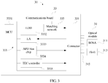
- an embodiment of the present invention provides an optical assembly 30, including an optical module 31 and a communications board 33.
- An optical component 311, a first memory 313, and an edge connector 315 connected to the optical component 311 and the first memory 313 are disposed on the optical module 31, and the first memory 313 is configured to store a first scattering parameter S1 of the optical module 31 and an operating parameter of the optical component 311.
- the first scattering parameter S1 is a scattering parameter (S parameter) of the optical module 31, including a backward transmission (isolation) coefficient S1 12 , a forward transmission (gain) coefficient S1 21 , an input reflection (input return loss) coefficient S1 11 , and an output reflection (output return loss) coefficient S1 22 .
- the operating parameter of the optical component 311 includes a bias current, a modulated current, a modulated voltage, an operating temperature, and a backlight diode current.
- the optical component 311 includes a bidirectional optical subassembly BOSA, or the optical component 311 may include a transmitter optical subassembly TOSA and a receiver optical subassembly ROSA.
- a connector 331, and an electronic chip 333 and a matching network 335 that correspond to the optical component are disposed on the communications board 33.
- the optical module 31 is connected to the connector 331 by using the edge connector 315.
- a pluggable connection is formed between the optical module 31 and the communications board 33 by using the edge connector 315.
- the electronic chip 333 includes a micro controller (Micro Control Unit, MCU) 3331, a laser diode driver (Laser Diode Driver, LDD) 3332, a limiting amplifier (Limiting Amplifier, LA) 3333, an avalanche photodiode (Avalanche Photodiode, APD) bias chip 3334, and a thermoelectric cooler (Thermoelectric Cooler, TEC) control chip 3335.
- MCU Micro Control Unit
- LDD Laser Diode Driver
- LA Limit Amplifier
- LA avalanche photodiode
- APD avalanche Photodiode
- TEC thermoelectric cooler
- the micro controller 3331 is electrically connected to the laser diode driver 3332, the limiting amplifier 3333, the avalanche photodiode bias chip 3334, the thermoelectric cooler control chip 3335, and the matching network 335, and is electrically connected to the first memory 313 by using the connector 331 and the edge connector 315.
- the laser diode driver 3332 is connected to the connector 331 via the matching network 335.
- the micro controller 3331 is electrically connected to another chip on the communications board 33 and the first memory 313 on the optical module 31 by using a control bus (for example, an I 2 C bus).
- the micro controller 3331 is configured to: read the operating parameter from the first memory 313, and configure the laser diode driver 3332 and the limiting amplifier 3333 based on the operating parameter.
- the laser diode driver 3332 is configured to drive the optical component 311 to transmit an optical signal.
- the limiting amplifier 3333 is configured to amplify a signal received by the optical component 311.
- the avalanche photodiode bias chip 3334 is configured to provide a bias voltage for the optical component 311.
- the thermoelectric cooler control chip 3335 is configured to provide a cooling current or a heating current for the optical module.
- the communications board 33 stores a second scattering parameter S2 that is between the laser diode driver 3332 and the connector 331.
- the second scattering parameter S2 may be stored in built-in storage space of the micro controller 3331 or in a second memory (not shown in the figure) disposed on the communications board 33.
- the second scattering parameter S2 is a scattering parameter (S parameter) between an output end of the laser diode driver 3332 and an end that is of the connector 331 and that is connected to the edge connector 315.
- the second scattering parameter includes a scattering parameter of the connector 331.
- the second scattering parameter also includes a backward transmission coefficient S2 12 , a forward transmission coefficient S2 21 , an input reflection coefficient S2 11 , and an output reflection coefficient S2 22 .
- the micro controller 3331 is further configured to: read the first scattering parameter from the first memory 313, calculate a third scattering parameter S3 that is between the laser diode driver 3332 and the optical module 31 based on the first scattering parameter and the second scattering parameter, and further adjust matched impedance of the matching network 335 based on the third scattering parameter S3.
- the third scattering parameter S3 is a scattering parameter (S parameter) between the output end of the laser diode driver 3332 and an output end of the optical module 31.
- the third scattering parameter includes a scattering parameter of the optical module 31.
- the third scattering parameter also includes a backward transmission coefficient S3 12 , a forward transmission coefficient S3 21 , an input reflection coefficient S3 11 , and an output reflection coefficient S3 22 .
- the calculating a third scattering parameter that is between the laser diode driver and the optical module based on the first scattering parameter and the second scattering parameter includes:
- the first scattering parameter is used as an example.
- the first scattering transmission parameter is T1.
- the second scattering transmission parameter T2 corresponding to the second scattering parameter may be calculated according to the foregoing formulas.
- the matching network 335 may include one or a combination of more of a resistor, an inductor, and a capacitor connected in series and/or connected in parallel, and the adjusting matched impedance of the matching network 335 is adjusting a value of the resistor, the inductor, or the capacitor.
- a value of at least one resistor, at least one inductor, or at least one capacitor in the matching network 335 is electrically adjustable.
- the adjusting matched impedance of the matching network of the optical assembly based on the third scattering parameter includes:
- a curve of the input reflection coefficient S3 11 of the third scattering parameter namely, an input return loss curve between the output end of the laser diode driver and the output end of the optical module, is generated. Then, a 3-dB bandwidth of the input return loss curve is calculated, and the 3-dB bandwidth of the input return loss curve is compared with the preset 3-dB bandwidth range. If the 3-dB bandwidth of the input return loss curve falls outside the preset 3-dB bandwidth range, it indicates that current matched impedance of the matching network needs to be adjusted. The micro controller may then control the electrically adjustable resistor, inductor, or capacitor in the matching network to change the value, thereby adjusting the matched impedance of the matching network.
- the third scattering parameter between the laser diode driver and the optical module is calculated by reading the first scattering parameter stored in the first memory and the second scattering parameter that is between the laser diode driver and the connector and that is stored on the communications board, and then the matched impedance of the matching network 335 between the laser diode driver and the connector is adjusted based on whether the 3-dB bandwidth of the curve corresponding to the third scattering parameter falls within the preset range, thereby implementing impedance matching between the laser diode driver and the optical module. This helps improve communication performance of the optical assembly.
- an embodiment of the present invention provides an optical assembly 30', including an optical module 31' and a communications board 33'.
- the optical module 31' differs from the optical module 31 in the embodiment shown in FIG. 3 in that the first memory 313 is configured to store an operating parameter of the optical component 311.
- the operating parameter includes a preset eye mask margin, a bias current, a modulated current, a modulated voltage, an operating temperature, a backlight diode current, and a monitor photodiode current.
- the communications board 33' differs from the communications board 33 in the embodiment shown in FIG. 3 in that an electronic chip 333' that is on the communications board 33' and that corresponds to the optical component 311 further includes an eye opening monitoring module 3336.
- the eye opening monitoring module 3336 is connected to the micro controller 3331, and is electrically connected to the optical module 31' by using the connector.
- the eye opening monitoring module 3336 is configured to: read an electrical signal output by a monitor photodiode (not shown in the figure) in the optical component 311, and measure, based on the electrical signal, an eye opening of a signal transmitted by the optical component 311.
- the micro controller 3331 is configured to: read the operating parameter from the first memory 313, and configure the laser diode driver 3332 and the limiting amplifier 3333 based on the operating parameter.
- the micro controller 3331 is further configured to: read the eye opening, and adjust matched impedance of the matching network 335 based on the eye opening and the preset eye mask margin in the operating parameter.
- the adjusting matched impedance of the matching network based on the eye opening and the preset eye mask margin includes:
- the eye opening of the signal transmitted by the optical component is measured, and the eye mask margin of the signal transmitted by the optical component is calculated based on the eye opening and a preset eye pattern mask. Further, whether the eye mask margin of the signal transmitted by the optical component falls within the preset eye mask margin range is determined. If the eye mask margin of the signal transmitted by the optical component falls within the preset eye mask margin range, it indicates that quality of the signal transmitted by the optical component meets a requirement. In other words, current matched impedance of the matching network already meets an impedance matching requirement, so that no adjustment is needed.
- the eye mask margin of the signal transmitted by the optical component falls outside the preset eye mask margin range, it indicates that quality of the signal transmitted by the optical component does not meet a requirement, so that the matched impedance of the matching network needs to be adjusted, to improve the quality of the transmitted signal.
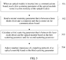
- an embodiment of the present invention provides a method for adjusting matched impedance of the optical assembly 30 in the embodiment shown in FIG. 3 .
- the method includes the following steps:
- the calculating a third scattering parameter that is between the laser diode driver and the optical module based on the first scattering parameter and the second scattering parameter includes:
- the adjusting matched impedance of a matching network of the optical assembly based on the third scattering parameter includes:
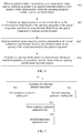
- an embodiment of the present invention provides a method for adjusting matched impedance of the optical assembly 30' in the embodiment shown in FIG. 4 .
- the method includes the following steps:
- Step 601 When an optical module is inserted into a communications board, read an operating parameter of an optical component stored in a first memory of the optical module, where the operating parameter includes a preset eye mask margin.
- Step 602 Configure an output parameter of a laser diode driver on the communications board based on the operating parameter of the optical component, and drive, by using the laser diode driver, the optical component to transmit an optical signal.
- Step 603 Read an electrical signal output by a monitor photodiode in the optical component, and measure, based on the electrical signal, an eye opening of the signal transmitted by the optical component.
- Step 604 Read the eye opening and the preset eye mask margin, and adjust matched impedance of the matching network based on the eye opening and the preset eye mask margin.
- the adjusting matched impedance of the matching network based on the eye opening and the preset eye mask margin includes:
- an embodiment of the present invention provides an apparatus 70 for adjusting matched impedance of the optical assembly 30 in the embodiment shown in FIG. 3 .
- the apparatus includes:
- the third-scattering-parameter calculation unit 703 is specifically configured to:
- the matched impedance adjustment unit 704 is specifically configured to:
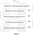
- an embodiment of the present invention provides an apparatus 80 for adjusting matched impedance of the optical assembly 30' in the embodiment shown in FIG. 4 .
- the apparatus includes:
- the matched impedance adjustment unit 804 is specifically configured to:
Landscapes
- Physics & Mathematics (AREA)
- Electromagnetism (AREA)
- Engineering & Computer Science (AREA)
- Computer Networks & Wireless Communication (AREA)
- Signal Processing (AREA)
- Optical Communication System (AREA)
- Optical Couplings Of Light Guides (AREA)
- Semiconductor Lasers (AREA)
Claims (15)
- Optische Anordnung (30, 40), umfassend ein optisches Modul (31) und eine Kommunikationsplatine (33), wobei
eine optische Komponente (311), ein erster Speicher (313) und ein mit der optischen Komponente und dem ersten Speicher verbundener Steckverbinder (315) auf dem optischen Modul angeordnet sind, und der erste Speicher konfiguriert ist, um einen ersten Streuparameter des optischen Moduls und einen Betriebsparameter der optischen Komponente zu speichern;
ein Verbinder und ein elektronischer Chip (333) und ein Anpassungsnetzwerk (335), die der optischen Komponente entsprechen, auf der Kommunikationsplatine angeordnet sind, und das optische Modul durch Verwenden des Steckverbinders mit dem Verbinder verbunden ist;
der elektronische Chip einen Mikrocontroller (3331) und einen Laserdiodentreiber (3332) umfasst, der Laserdiodentreiber über das Anpassungsnetzwerk mit dem Verbinder verbunden ist, und die Kommunikationsplatine einen zweiten Streuparameter speichert, der zwischen dem Laserdiodentreiber und dem Verbinder liegt, und
der Mikrocontroller zu Folgendem konfiguriert ist: Auslesen des ersten Streuparameters aus dem ersten Speicher, Berechnen eines dritten Streuparameters, der zwischen dem Laserdiodentreiber und dem optischen Modul basierend auf dem ersten Streuparameter und dem zweiten Streuparameter liegt, und ferner Angleichen der angepassten Impedanz des Anpassungsnetzwerks basierend auf dem dritten Streuparameter. - Optische Anordnung nach Anspruch 1, wobei der elektronische Chip ferner Folgendes umfasst:einen Lawinenfotodioden-Vorspannungschip, der konfiguriert ist, um eine Vorspannung für die optische Komponente bereitzustellen;einen Begrenzungsverstärker, der konfiguriert ist, um ein durch die optische Komponente empfangenes Signal zu verstärken; undeinen Steuerchip für einen thermoelektrischen Kühler, der konfiguriert ist, um einen Kühlstrom oder einen Heizstrom für das optische Modul bereitzustellen.
- Optische Anordnung nach Anspruch 2, wobei der Betriebsparameter der optischen Komponente einen Vorspannungsstrom, einen modulierten Strom, eine modulierte Spannung, eine Betriebstemperatur und einen Hintergrundbeleuchtungsdiodenstrom umfasst; der Mikrocontroller ferner zu Folgendem konfiguriert ist: Auslesen des Betriebsparameters aus dem ersten Speicher und Konfigurieren des Laserdiodentreibers und des Begrenzungsverstärkers basierend auf dem Betriebsparameter; und wobei der Laserdiodentreiber konfiguriert ist, um die optische Komponente zu treiben, um ein optisches Signal zu übertragen.
- Optische Anordnung nach einem der Ansprüche 1 bis 3, wobei das Berechnen eines dritten Streuparameters, der zwischen dem Laserdiodentreiber und dem optischen Modul liegt, basierend auf dem ersten Streuparameter und dem zweiten Streuparameter Folgendes umfasst:Umwandeln des ersten Streuparameters in einen entsprechenden ersten Streuübertragungsparameter, und Umwandeln des zweiten Streuparameters in einen zweiten Streuübertragungsparameter;Multiplizieren des ersten Streuübertragungsparameters mit dem zweiten Streuübertragungsparameter, um einen dritten Streuübertragungsparameter zu erhalten; undUmwandeln des dritten Streuungsübertragungsparameters in den entsprechenden dritten Streuparameter.
- Optische Anordnung nach einem der Ansprüche 1 bis 3, wobei das Anpassungsnetzwerk einen oder eine Kombination aus einem Widerstand, einer Induktivität und einem Kondensator umfasst, die in Reihe geschaltet und/oder parallel geschaltet sind, und die angleichende angepasste Impedanz des Anpassungsnetzwerks einen Wert des Widerstands, der Induktivität oder des Kondensators angleicht.
- Optische Anordnung nach einem der Ansprüche 1 bis 3, wobei die optische Komponente eine bidirektionale optische Untergruppe (bidirectional optical subassembly- BOSA) umfasst oder die optische Komponente eine optische Senderuntergruppe (transmitter optical subassembly - TOSA) und eine optische Empfängeruntergruppe (receiver optical subassembly - ROSA) umfasst.
- Optische Anordnung, umfassend ein optisches Modul und eine Kommunikationsplatine, wobei
eine optische Komponente, ein erster Speicher und ein mit der optischen Komponente verbundener Steckverbinder und der erste Speicher auf dem optischen Modul angeordnet sind, wobei der erste Speicher konfiguriert ist, um einen Betriebsparameter der optischen Komponente zu speichern, und der Betriebsparameter einen voreingestellten Augenmaskenrand umfasst;
ein Verbinder und ein elektronischer Chip und ein Anpassungsnetzwerk, die der optischen Komponente entsprechen, auf der Kommunikationsplatine angeordnet sind, und das optische Modul durch Verwenden des Steckverbinders mit dem Verbinder verbunden ist;
der elektronische Chip einen Mikrocontroller, einen Laserdiodentreiber und ein Augenöffnungsüberwachungsmodul umfasst; der Mikrocontroller mit dem Laserdiodentreiber, dem Augenöffnungsüberwachungsmodul und dem Anpassungsnetzwerk elektrisch verbunden ist; und der Laserdiodentreiber über das Anpassungsnetzwerk mit dem Verbinder verbunden ist;
das Augenöffnungsüberwachungsmodul zu Folgendem konfiguriert ist: Auslesen eines durch eine Überwachungsfotodiode in der optischen Komponente ausgegebenen elektrischen Signals und basierend auf dem elektrischen Signal, Messen einer Augenöffnung eines durch die optische Komponente übertragenen Signals; und
der Mikrocontroller zu Folgendem konfiguriert ist: Auslesen der Augenöffnung und des voreingestellten Augenmaskenrands und Angleichen der angepassten Impedanz des Anpassungsnetzwerks basierend auf der Augenöffnung und dem voreingestellten Augenmaskenrand. - Optische Anordnung nach Anspruch 7, wobei der elektronische Chip ferner Folgendes umfasst:einen Lawinenfotodioden-Vorspannungschip, der konfiguriert ist, um eine Vorspannung für die optische Komponente bereitzustellen;einen Begrenzungsverstärker, der konfiguriert ist, um ein durch die optische Komponente empfangenes Signal zu verstärken; undeinen Steuerchip für einen thermoelektrischen Kühler, der konfiguriert ist, um einen Kühlstrom oder einen Heizstrom für das optische Modul bereitzustellen.
- Optische Anordnung nach Anspruch 8, wobei der Betriebsparameter der optischen Komponente ferner einen Vorspannungsstrom, einen modulierten Strom, eine modulierte Spannung, eine Betriebstemperatur, einen Hintergrundbeleuchtungsdiodenstrom und einen Überwachungsfotodiodenstrom umfasst; der Mikrocontroller ferner konfiguriert ist, um den Laserdiodentreiber und den Begrenzungsverstärker basierend auf dem Betriebsparameter zu konfigurieren; und der Laserdiodentreiber konfiguriert ist, um die optische Komponente zu treiben, um ein optisches Signal zu übertragen.
- Optische Anordnung nach einem der Ansprüche 7 bis 9, wobei das Anpassungsnetzwerk einen oder eine Kombination aus einem Widerstand, einer Induktivität und einem Kondensator umfasst, die in Reihe geschaltet und/oder parallel geschaltet sind, und die angleichende angepasste Impedanz des Anpassungsnetzwerks einen Wert des Widerstands, der Induktivität oder des Kondensators angleicht.
- Optische Anordnung nach einem der Ansprüche 7 bis 9, wobei die optische Komponente eine bidirektionale optische Untergruppe (BOSA) umfasst oder die optische Komponente eine optische Senderuntergruppe (TOSA) und eine optische Empfängeruntergruppe (ROSA) umfasst.
- Passives optisches Netzwerksystem, umfassend ein optisches Leitungsendgerät, ein optisches Verteilungsnetzwerk und eine optische Netzwerkeinheit, wobei das optische Leitungsendgerät über das optische Verteilungsnetzwerk mit der optischen Netzwerkeinheit verbunden ist, und das optische Leitungsendgerät die optische Anordnung nach einem der Ansprüche 1 bis 6 umfasst und/oder die optische Netzwerkeinheit die optische Anordnung nach einem der Ansprüche 7 bis 11 umfasst.
- Verfahren zum Angleichen der angepassten Impedanz der optischen Anordnung nach einem der Ansprüche 1 bis 6, Folgendes umfassend:wenn ein optisches Modul in eine Kommunikationsplatine eingesetzt wird, Auslesen eines ersten Streuparameters des in einem ersten Speicher des optischen Moduls gespeicherten optischen Moduls;Auslesen eines zweiten Streuparameters, der zwischen einem Laserdiodentreiber und einem Verbinder liegt und auf der Kommunikationsplatine gespeichert ist;Berechnen eines dritten Streuparameters, der zwischen dem Laserdiodentreiber und dem optischen Modul liegt, basierend auf dem ersten Streuparameter und dem zweiten Streuparameter; undAngleichen der angepassten Impedanz eines Anpassungsnetzwerks der optischen Anordnung basierend auf dem dritten Streuparameter.
- Verfahren nach Anspruch 13, wobei das Berechnen eines dritten Streuparameters, der zwischen dem Laserdiodentreiber und dem optischen Modul liegt, basierend auf dem ersten Streuparameter und dem zweiten Streuparameter, Folgendes umfasst:Umwandeln des ersten Streuparameters in einen entsprechenden ersten Streuübertragungsparameter, und Umwandeln des zweiten Streuparameters in einen zweiten Streuübertragungsparameter;Multiplizieren des ersten Streuübertragungsparameters mit dem zweiten Streuübertragungsparameter, um einen dritten Streuübertragungsparameter zu erhalten; undUmwandeln des dritten Streuungsübertragungsparameters in den entsprechenden dritten Streuparameter.
- Verfahren nach Anspruch 13, wobei das Angleichen der angepassten Impedanz eines Anpassungsnetzwerks der optischen Anordnung, basierend auf dem dritten Streuparameter, Folgendes umfasst:Berechnen einer 3-dB-Bandbreite einer dem dritten Streuparameter entsprechenden Kurve;Bestimmen, ob die 3-dB-Bandbreite der dem dritten Streuparameter entsprechenden Kurve innerhalb eines voreingestellten 3-dB-Bandbreitenbereichs fällt; undfalls die 3-dB-Bandbreite der dem dritten Streuparameter entsprechenden Kurve außerhalb des voreingestellten 3-dB-Bandbreitenbereichs fällt, Angleichen der angepassten Impedanz der optischen Anordnung durch Angleichen eines Wertes eines Widerstands, einer Induktivität oder eines Kondensators in dem Anpassungsnetzwerk auf der Kommunikationsplatine.
Applications Claiming Priority (1)
| Application Number | Priority Date | Filing Date | Title |
|---|---|---|---|
| PCT/CN2017/075273 WO2018157317A1 (zh) | 2017-02-28 | 2017-02-28 | 无源光网络系统、光组件及其匹配阻抗调整方法 |
Publications (3)
| Publication Number | Publication Date |
|---|---|
| EP3573258A1 EP3573258A1 (de) | 2019-11-27 |
| EP3573258A4 EP3573258A4 (de) | 2020-04-08 |
| EP3573258B1 true EP3573258B1 (de) | 2021-03-17 |
Family
ID=63369615
Family Applications (1)
| Application Number | Title | Priority Date | Filing Date |
|---|---|---|---|
| EP17899120.4A Active EP3573258B1 (de) | 2017-02-28 | 2017-02-28 | Passives optisches netzwerksystem und optische komponente und passendes impedanzanpassungsverfahren dafür |
Country Status (3)
| Country | Link |
|---|---|
| EP (1) | EP3573258B1 (de) |
| CN (1) | CN110192358B (de) |
| WO (1) | WO2018157317A1 (de) |
Families Citing this family (8)
| Publication number | Priority date | Publication date | Assignee | Title |
|---|---|---|---|---|
| CN112925068B (zh) * | 2019-12-06 | 2023-05-05 | 青岛海信宽带多媒体技术有限公司 | 一种光模块 |
| CN112398541B (zh) * | 2020-11-05 | 2022-05-17 | 青岛海信宽带多媒体技术有限公司 | 一种光模块 |
| WO2022057866A1 (zh) * | 2020-09-17 | 2022-03-24 | 青岛海信宽带多媒体技术有限公司 | 一种光模块 |
| CN113092867A (zh) * | 2021-03-29 | 2021-07-09 | 上海橙科微电子科技有限公司 | 通过方波测试光模块发送系统阻抗的连续性的方法、系统及介质 |
| CN115314105B (zh) * | 2022-07-06 | 2023-07-21 | 江苏信而泰智能装备有限公司 | Bob测试系统 |
| CN118368546A (zh) * | 2023-01-18 | 2024-07-19 | 华为技术有限公司 | 信号传输装置、信号传输装置的调测方法及设备 |
| CN118827249A (zh) * | 2023-04-20 | 2024-10-22 | 华为技术有限公司 | 通信方法、通信设备、直驱模块和通信系统 |
| CN118367436B (zh) * | 2024-06-19 | 2024-10-01 | 四川泰瑞创通讯技术股份有限公司 | 优化激光器打线阻抗匹配的光模块 |
Family Cites Families (7)
| Publication number | Priority date | Publication date | Assignee | Title |
|---|---|---|---|---|
| US7486894B2 (en) * | 2002-06-25 | 2009-02-03 | Finisar Corporation | Transceiver module and integrated circuit with dual eye openers |
| US7526207B2 (en) * | 2002-10-18 | 2009-04-28 | Finisar Corporation | Flexible circuit design for improved laser bias connections to optical subassemblies |
| US8422891B2 (en) * | 2010-09-24 | 2013-04-16 | Intel Corporation | Jitter reduction of electrical signals from limiting optical modules |
| CN102299746B (zh) * | 2011-07-08 | 2014-06-25 | 成都新易盛通信技术股份有限公司 | 一种低成本带高精度数字诊断功能的sfp模块 |
| CN203632683U (zh) * | 2013-11-27 | 2014-06-04 | 青岛海信宽带多媒体技术有限公司 | 光信号接收丢失迟滞参数调整电路及光模块 |
| CN106059673A (zh) * | 2016-05-18 | 2016-10-26 | 青岛海信宽带多媒体技术有限公司 | 一种光模块及光线路终端设备 |
| CN106125213B (zh) * | 2016-08-26 | 2018-08-17 | 青岛海信宽带多媒体技术有限公司 | 一种光模块 |
-
2017
- 2017-02-28 CN CN201780084156.4A patent/CN110192358B/zh active Active
- 2017-02-28 WO PCT/CN2017/075273 patent/WO2018157317A1/zh not_active Ceased
- 2017-02-28 EP EP17899120.4A patent/EP3573258B1/de active Active
Non-Patent Citations (1)
| Title |
|---|
| None * |
Also Published As
| Publication number | Publication date |
|---|---|
| EP3573258A1 (de) | 2019-11-27 |
| CN110192358B (zh) | 2020-12-15 |
| EP3573258A4 (de) | 2020-04-08 |
| WO2018157317A1 (zh) | 2018-09-07 |
| CN110192358A (zh) | 2019-08-30 |
Similar Documents
| Publication | Publication Date | Title |
|---|---|---|
| EP3573258B1 (de) | Passives optisches netzwerksystem und optische komponente und passendes impedanzanpassungsverfahren dafür | |
| EP2602946B1 (de) | Bidirektionales optisches einzelfasermodul und passives optisches netzwerksystem | |
| CN105144508B (zh) | 温控多信道光发射次模块以及具有此温控多信道光发射次模块的光收发器模块 | |
| CA2722400C (en) | Method and apparatus for controlling the optical output power from a burst mode laser | |
| US7751712B2 (en) | Passive optical network and data communication method thereof | |
| US9964720B2 (en) | Monitoring and controlling temperature across a laser array in a transmitter optical subassembly (TOSA) package | |
| CN105247400B (zh) | 紧凑型多信道光收发器模块 | |
| CN107710648B (zh) | 具有热阵列波导光栅多路复用器和无热阵列波导光栅解复用器的多通道光收发器模块 | |
| US20090169209A1 (en) | Network system, optical line terminating apparatus, and optical network apparatus | |
| US20130202300A1 (en) | Optical line terminal (olt) optical module adapted to perform optical unit network (onu) functionality | |
| CN105518949A (zh) | 用于光发射器系统的提高效率的加热激光器封装 | |
| CN102523540B (zh) | 光模块及具有该光模块的无源光网络 | |
| CN102511138B (zh) | 可调光收发器、无源光网络系统及设备 | |
| US9106050B2 (en) | Self-characterization tunable optical network unit | |
| JP2010166279A (ja) | 光通信システムおよび光集線装置 | |
| US9287989B2 (en) | Optical data transmission device | |
| US8340519B2 (en) | Passive optical network comprising an optical burst mode receiver | |
| CN211127812U (zh) | 一种自带mac的sfp+光模块 | |
| WO2015042842A1 (zh) | 光发射系统 | |
| US12382203B2 (en) | Optical communication apparatus and optical communication method | |
| WO2017173619A1 (zh) | 激光器件驱动电流补偿方法及相关装置、组件和系统 | |
| CN201315587Y (zh) | 一种单纤三向模块 | |
| CN223024424U (zh) | 光组件在板装置、主网关和fttr系统 | |
| WO2020238279A1 (zh) | 一种plc芯片、tosa、bosa、光模块、以及光网络设备 |
Legal Events
| Date | Code | Title | Description |
|---|---|---|---|
| STAA | Information on the status of an ep patent application or granted ep patent |
Free format text: STATUS: THE INTERNATIONAL PUBLICATION HAS BEEN MADE |
|
| PUAI | Public reference made under article 153(3) epc to a published international application that has entered the european phase |
Free format text: ORIGINAL CODE: 0009012 |
|
| STAA | Information on the status of an ep patent application or granted ep patent |
Free format text: STATUS: REQUEST FOR EXAMINATION WAS MADE |
|
| 17P | Request for examination filed |
Effective date: 20190821 |
|
| AK | Designated contracting states |
Kind code of ref document: A1 Designated state(s): AL AT BE BG CH CY CZ DE DK EE ES FI FR GB GR HR HU IE IS IT LI LT LU LV MC MK MT NL NO PL PT RO RS SE SI SK SM TR |
|
| AX | Request for extension of the european patent |
Extension state: BA ME |
|
| A4 | Supplementary search report drawn up and despatched |
Effective date: 20200305 |
|
| RIC1 | Information provided on ipc code assigned before grant |
Ipc: H04B 10/40 20130101AFI20200228BHEP Ipc: G02B 6/42 20060101ALI20200228BHEP |
|
| DAV | Request for validation of the european patent (deleted) | ||
| DAX | Request for extension of the european patent (deleted) | ||
| GRAP | Despatch of communication of intention to grant a patent |
Free format text: ORIGINAL CODE: EPIDOSNIGR1 |
|
| STAA | Information on the status of an ep patent application or granted ep patent |
Free format text: STATUS: GRANT OF PATENT IS INTENDED |
|
| INTG | Intention to grant announced |
Effective date: 20201016 |
|
| GRAS | Grant fee paid |
Free format text: ORIGINAL CODE: EPIDOSNIGR3 |
|
| GRAA | (expected) grant |
Free format text: ORIGINAL CODE: 0009210 |
|
| STAA | Information on the status of an ep patent application or granted ep patent |
Free format text: STATUS: THE PATENT HAS BEEN GRANTED |
|
| AK | Designated contracting states |
Kind code of ref document: B1 Designated state(s): AL AT BE BG CH CY CZ DE DK EE ES FI FR GB GR HR HU IE IS IT LI LT LU LV MC MK MT NL NO PL PT RO RS SE SI SK SM TR |
|
| REG | Reference to a national code |
Ref country code: GB Ref legal event code: FG4D |
|
| REG | Reference to a national code |
Ref country code: CH Ref legal event code: EP |
|
| REG | Reference to a national code |
Ref country code: DE Ref legal event code: R096 Ref document number: 602017035024 Country of ref document: DE |
|
| REG | Reference to a national code |
Ref country code: IE Ref legal event code: FG4D |
|
| REG | Reference to a national code |
Ref country code: AT Ref legal event code: REF Ref document number: 1373232 Country of ref document: AT Kind code of ref document: T Effective date: 20210415 |
|
| REG | Reference to a national code |
Ref country code: LT Ref legal event code: MG9D |
|
| PG25 | Lapsed in a contracting state [announced via postgrant information from national office to epo] |
Ref country code: BG Free format text: LAPSE BECAUSE OF FAILURE TO SUBMIT A TRANSLATION OF THE DESCRIPTION OR TO PAY THE FEE WITHIN THE PRESCRIBED TIME-LIMIT Effective date: 20210617 Ref country code: FI Free format text: LAPSE BECAUSE OF FAILURE TO SUBMIT A TRANSLATION OF THE DESCRIPTION OR TO PAY THE FEE WITHIN THE PRESCRIBED TIME-LIMIT Effective date: 20210317 Ref country code: HR Free format text: LAPSE BECAUSE OF FAILURE TO SUBMIT A TRANSLATION OF THE DESCRIPTION OR TO PAY THE FEE WITHIN THE PRESCRIBED TIME-LIMIT Effective date: 20210317 Ref country code: GR Free format text: LAPSE BECAUSE OF FAILURE TO SUBMIT A TRANSLATION OF THE DESCRIPTION OR TO PAY THE FEE WITHIN THE PRESCRIBED TIME-LIMIT Effective date: 20210618 Ref country code: NO Free format text: LAPSE BECAUSE OF FAILURE TO SUBMIT A TRANSLATION OF THE DESCRIPTION OR TO PAY THE FEE WITHIN THE PRESCRIBED TIME-LIMIT Effective date: 20210617 |
|
| REG | Reference to a national code |
Ref country code: AT Ref legal event code: MK05 Ref document number: 1373232 Country of ref document: AT Kind code of ref document: T Effective date: 20210317 |
|
| REG | Reference to a national code |
Ref country code: NL Ref legal event code: MP Effective date: 20210317 |
|
| PG25 | Lapsed in a contracting state [announced via postgrant information from national office to epo] |
Ref country code: RS Free format text: LAPSE BECAUSE OF FAILURE TO SUBMIT A TRANSLATION OF THE DESCRIPTION OR TO PAY THE FEE WITHIN THE PRESCRIBED TIME-LIMIT Effective date: 20210317 Ref country code: LV Free format text: LAPSE BECAUSE OF FAILURE TO SUBMIT A TRANSLATION OF THE DESCRIPTION OR TO PAY THE FEE WITHIN THE PRESCRIBED TIME-LIMIT Effective date: 20210317 Ref country code: SE Free format text: LAPSE BECAUSE OF FAILURE TO SUBMIT A TRANSLATION OF THE DESCRIPTION OR TO PAY THE FEE WITHIN THE PRESCRIBED TIME-LIMIT Effective date: 20210317 |
|
| PG25 | Lapsed in a contracting state [announced via postgrant information from national office to epo] |
Ref country code: NL Free format text: LAPSE BECAUSE OF FAILURE TO SUBMIT A TRANSLATION OF THE DESCRIPTION OR TO PAY THE FEE WITHIN THE PRESCRIBED TIME-LIMIT Effective date: 20210317 |
|
| PG25 | Lapsed in a contracting state [announced via postgrant information from national office to epo] |
Ref country code: CZ Free format text: LAPSE BECAUSE OF FAILURE TO SUBMIT A TRANSLATION OF THE DESCRIPTION OR TO PAY THE FEE WITHIN THE PRESCRIBED TIME-LIMIT Effective date: 20210317 Ref country code: EE Free format text: LAPSE BECAUSE OF FAILURE TO SUBMIT A TRANSLATION OF THE DESCRIPTION OR TO PAY THE FEE WITHIN THE PRESCRIBED TIME-LIMIT Effective date: 20210317 Ref country code: LT Free format text: LAPSE BECAUSE OF FAILURE TO SUBMIT A TRANSLATION OF THE DESCRIPTION OR TO PAY THE FEE WITHIN THE PRESCRIBED TIME-LIMIT Effective date: 20210317 Ref country code: SM Free format text: LAPSE BECAUSE OF FAILURE TO SUBMIT A TRANSLATION OF THE DESCRIPTION OR TO PAY THE FEE WITHIN THE PRESCRIBED TIME-LIMIT Effective date: 20210317 Ref country code: AT Free format text: LAPSE BECAUSE OF FAILURE TO SUBMIT A TRANSLATION OF THE DESCRIPTION OR TO PAY THE FEE WITHIN THE PRESCRIBED TIME-LIMIT Effective date: 20210317 |
|
| PG25 | Lapsed in a contracting state [announced via postgrant information from national office to epo] |
Ref country code: PT Free format text: LAPSE BECAUSE OF FAILURE TO SUBMIT A TRANSLATION OF THE DESCRIPTION OR TO PAY THE FEE WITHIN THE PRESCRIBED TIME-LIMIT Effective date: 20210719 Ref country code: PL Free format text: LAPSE BECAUSE OF FAILURE TO SUBMIT A TRANSLATION OF THE DESCRIPTION OR TO PAY THE FEE WITHIN THE PRESCRIBED TIME-LIMIT Effective date: 20210317 Ref country code: SK Free format text: LAPSE BECAUSE OF FAILURE TO SUBMIT A TRANSLATION OF THE DESCRIPTION OR TO PAY THE FEE WITHIN THE PRESCRIBED TIME-LIMIT Effective date: 20210317 Ref country code: RO Free format text: LAPSE BECAUSE OF FAILURE TO SUBMIT A TRANSLATION OF THE DESCRIPTION OR TO PAY THE FEE WITHIN THE PRESCRIBED TIME-LIMIT Effective date: 20210317 Ref country code: IS Free format text: LAPSE BECAUSE OF FAILURE TO SUBMIT A TRANSLATION OF THE DESCRIPTION OR TO PAY THE FEE WITHIN THE PRESCRIBED TIME-LIMIT Effective date: 20210717 |
|
| REG | Reference to a national code |
Ref country code: DE Ref legal event code: R097 Ref document number: 602017035024 Country of ref document: DE |
|
| PLBE | No opposition filed within time limit |
Free format text: ORIGINAL CODE: 0009261 |
|
| STAA | Information on the status of an ep patent application or granted ep patent |
Free format text: STATUS: NO OPPOSITION FILED WITHIN TIME LIMIT |
|
| PG25 | Lapsed in a contracting state [announced via postgrant information from national office to epo] |
Ref country code: AL Free format text: LAPSE BECAUSE OF FAILURE TO SUBMIT A TRANSLATION OF THE DESCRIPTION OR TO PAY THE FEE WITHIN THE PRESCRIBED TIME-LIMIT Effective date: 20210317 Ref country code: DK Free format text: LAPSE BECAUSE OF FAILURE TO SUBMIT A TRANSLATION OF THE DESCRIPTION OR TO PAY THE FEE WITHIN THE PRESCRIBED TIME-LIMIT Effective date: 20210317 Ref country code: ES Free format text: LAPSE BECAUSE OF FAILURE TO SUBMIT A TRANSLATION OF THE DESCRIPTION OR TO PAY THE FEE WITHIN THE PRESCRIBED TIME-LIMIT Effective date: 20210317 |
|
| 26N | No opposition filed |
Effective date: 20211220 |
|
| PG25 | Lapsed in a contracting state [announced via postgrant information from national office to epo] |
Ref country code: SI Free format text: LAPSE BECAUSE OF FAILURE TO SUBMIT A TRANSLATION OF THE DESCRIPTION OR TO PAY THE FEE WITHIN THE PRESCRIBED TIME-LIMIT Effective date: 20210317 |
|
| PG25 | Lapsed in a contracting state [announced via postgrant information from national office to epo] |
Ref country code: IT Free format text: LAPSE BECAUSE OF FAILURE TO SUBMIT A TRANSLATION OF THE DESCRIPTION OR TO PAY THE FEE WITHIN THE PRESCRIBED TIME-LIMIT Effective date: 20210317 |
|
| PG25 | Lapsed in a contracting state [announced via postgrant information from national office to epo] |
Ref country code: IS Free format text: LAPSE BECAUSE OF FAILURE TO SUBMIT A TRANSLATION OF THE DESCRIPTION OR TO PAY THE FEE WITHIN THE PRESCRIBED TIME-LIMIT Effective date: 20210717 |
|
| REG | Reference to a national code |
Ref country code: DE Ref legal event code: R119 Ref document number: 602017035024 Country of ref document: DE |
|
| PG25 | Lapsed in a contracting state [announced via postgrant information from national office to epo] |
Ref country code: MC Free format text: LAPSE BECAUSE OF FAILURE TO SUBMIT A TRANSLATION OF THE DESCRIPTION OR TO PAY THE FEE WITHIN THE PRESCRIBED TIME-LIMIT Effective date: 20210317 |
|
| REG | Reference to a national code |
Ref country code: CH Ref legal event code: PL |
|
| REG | Reference to a national code |
Ref country code: BE Ref legal event code: MM Effective date: 20220228 |
|
| PG25 | Lapsed in a contracting state [announced via postgrant information from national office to epo] |
Ref country code: LU Free format text: LAPSE BECAUSE OF NON-PAYMENT OF DUE FEES Effective date: 20220228 |
|
| PG25 | Lapsed in a contracting state [announced via postgrant information from national office to epo] |
Ref country code: FR Free format text: LAPSE BECAUSE OF NON-PAYMENT OF DUE FEES Effective date: 20220228 |
|
| PG25 | Lapsed in a contracting state [announced via postgrant information from national office to epo] |
Ref country code: LI Free format text: LAPSE BECAUSE OF NON-PAYMENT OF DUE FEES Effective date: 20220228 Ref country code: IE Free format text: LAPSE BECAUSE OF NON-PAYMENT OF DUE FEES Effective date: 20220228 Ref country code: DE Free format text: LAPSE BECAUSE OF NON-PAYMENT OF DUE FEES Effective date: 20220901 Ref country code: CH Free format text: LAPSE BECAUSE OF NON-PAYMENT OF DUE FEES Effective date: 20220228 |
|
| PG25 | Lapsed in a contracting state [announced via postgrant information from national office to epo] |
Ref country code: BE Free format text: LAPSE BECAUSE OF NON-PAYMENT OF DUE FEES Effective date: 20220228 |
|
| PG25 | Lapsed in a contracting state [announced via postgrant information from national office to epo] |
Ref country code: MK Free format text: LAPSE BECAUSE OF FAILURE TO SUBMIT A TRANSLATION OF THE DESCRIPTION OR TO PAY THE FEE WITHIN THE PRESCRIBED TIME-LIMIT Effective date: 20210317 Ref country code: CY Free format text: LAPSE BECAUSE OF FAILURE TO SUBMIT A TRANSLATION OF THE DESCRIPTION OR TO PAY THE FEE WITHIN THE PRESCRIBED TIME-LIMIT Effective date: 20210317 |
|
| PG25 | Lapsed in a contracting state [announced via postgrant information from national office to epo] |
Ref country code: HU Free format text: LAPSE BECAUSE OF FAILURE TO SUBMIT A TRANSLATION OF THE DESCRIPTION OR TO PAY THE FEE WITHIN THE PRESCRIBED TIME-LIMIT; INVALID AB INITIO Effective date: 20170228 |
|
| PG25 | Lapsed in a contracting state [announced via postgrant information from national office to epo] |
Ref country code: MT Free format text: LAPSE BECAUSE OF FAILURE TO SUBMIT A TRANSLATION OF THE DESCRIPTION OR TO PAY THE FEE WITHIN THE PRESCRIBED TIME-LIMIT Effective date: 20210317 |
|
| PG25 | Lapsed in a contracting state [announced via postgrant information from national office to epo] |
Ref country code: TR Free format text: LAPSE BECAUSE OF FAILURE TO SUBMIT A TRANSLATION OF THE DESCRIPTION OR TO PAY THE FEE WITHIN THE PRESCRIBED TIME-LIMIT Effective date: 20210317 |
|
| PGFP | Annual fee paid to national office [announced via postgrant information from national office to epo] |
Ref country code: GB Payment date: 20260106 Year of fee payment: 10 |