EP3573118A1 - Organic electroluminescent device and fabrication method thereof - Google Patents
Organic electroluminescent device and fabrication method thereof Download PDFInfo
- Publication number
- EP3573118A1 EP3573118A1 EP18741504.7A EP18741504A EP3573118A1 EP 3573118 A1 EP3573118 A1 EP 3573118A1 EP 18741504 A EP18741504 A EP 18741504A EP 3573118 A1 EP3573118 A1 EP 3573118A1
- Authority
- EP
- European Patent Office
- Prior art keywords
- host material
- ring
- organic electroluminescent
- electroluminescent device
- acceptor
- Prior art date
- Legal status (The legal status is an assumption and is not a legal conclusion. Google has not performed a legal analysis and makes no representation as to the accuracy of the status listed.)
- Granted
Links
- CNIHTUDVSIDNEV-UHFFFAOYSA-N CN1c(cc(c(cccc2)c2[n]2-c(cc3)ncc3P(c3ccccn3)([n]3c(cc4Sc(cccc5)c5N(C)c4c4)c4c4ccccc34)=O)c2c2)c2Sc2c1cccc2 Chemical compound CN1c(cc(c(cccc2)c2[n]2-c(cc3)ncc3P(c3ccccn3)([n]3c(cc4Sc(cccc5)c5N(C)c4c4)c4c4ccccc34)=O)c2c2)c2Sc2c1cccc2 CNIHTUDVSIDNEV-UHFFFAOYSA-N 0.000 description 1
- QOZVFHKAFOKHCF-UHFFFAOYSA-N CN1c(cc(c2ccccc2[n]2-c(cc3)ccc3P(c3ccccc3)([n]3c(cc4N(C)c(cccc5)c5N(C)c4c4)c4c4c3cccc4)=O)c2c2)c2N(C)c2ccccc12 Chemical compound CN1c(cc(c2ccccc2[n]2-c(cc3)ccc3P(c3ccccc3)([n]3c(cc4N(C)c(cccc5)c5N(C)c4c4)c4c4c3cccc4)=O)c2c2)c2N(C)c2ccccc12 QOZVFHKAFOKHCF-UHFFFAOYSA-N 0.000 description 1
- OUACRTXDOPHJII-UHFFFAOYSA-N C[n](c1c2cccc1)c(cc1)c2c(c2ccccc22)c1[n]2-c(cc1)ccc1P(c1ncccc1)([n](c1ccccc11)c(cc2)c1c1c2[n](C)c2ccccc12)=O Chemical compound C[n](c1c2cccc1)c(cc1)c2c(c2ccccc22)c1[n]2-c(cc1)ccc1P(c1ncccc1)([n](c1ccccc11)c(cc2)c1c1c2[n](C)c2ccccc12)=O OUACRTXDOPHJII-UHFFFAOYSA-N 0.000 description 1
- FDHBMNWKCFTUJE-UHFFFAOYSA-N O=P(c1ccccc1)(c(cc1)ccc1-[n](c1ccccc1c1c2)c1cc1c2Oc2ccccc2S1)[n]1c(cc2Sc(cccc3)c3Oc2c2)c2c2ccccc12 Chemical compound O=P(c1ccccc1)(c(cc1)ccc1-[n](c1ccccc1c1c2)c1cc1c2Oc2ccccc2S1)[n]1c(cc2Sc(cccc3)c3Oc2c2)c2c2ccccc12 FDHBMNWKCFTUJE-UHFFFAOYSA-N 0.000 description 1
- ONIPNQLHRISTMA-UHFFFAOYSA-N O=P(c1ccccc1)(c(cc1)ccc1-[n]1c(cc2[o]c(cccc3)c3c2c2)c2c2ccccc12)[n]1c(cc2[o]c3ccccc3c2c2)c2c2c1cccc2 Chemical compound O=P(c1ccccc1)(c(cc1)ccc1-[n]1c(cc2[o]c(cccc3)c3c2c2)c2c2ccccc12)[n]1c(cc2[o]c3ccccc3c2c2)c2c2c1cccc2 ONIPNQLHRISTMA-UHFFFAOYSA-N 0.000 description 1
- YPOCHICPBKUPLN-UHFFFAOYSA-N O=P(c1ccccc1)(c1ccc(-[n]2c3ccc4[s]c(cccc5)c5c4c3c3c2cccc3)nc1)[n](c1ccccc11)c(cc2)c1c1c2[s]c2ccccc12 Chemical compound O=P(c1ccccc1)(c1ccc(-[n]2c3ccc4[s]c(cccc5)c5c4c3c3c2cccc3)nc1)[n](c1ccccc11)c(cc2)c1c1c2[s]c2ccccc12 YPOCHICPBKUPLN-UHFFFAOYSA-N 0.000 description 1
Images


Classifications
-
- C—CHEMISTRY; METALLURGY
- C07—ORGANIC CHEMISTRY
- C07D—HETEROCYCLIC COMPOUNDS
- C07D491/00—Heterocyclic compounds containing in the condensed ring system both one or more rings having oxygen atoms as the only ring hetero atoms and one or more rings having nitrogen atoms as the only ring hetero atoms, not provided for by groups C07D451/00 - C07D459/00, C07D463/00, C07D477/00 or C07D489/00
- C07D491/02—Heterocyclic compounds containing in the condensed ring system both one or more rings having oxygen atoms as the only ring hetero atoms and one or more rings having nitrogen atoms as the only ring hetero atoms, not provided for by groups C07D451/00 - C07D459/00, C07D463/00, C07D477/00 or C07D489/00 in which the condensed system contains two hetero rings
- C07D491/04—Ortho-condensed systems
- C07D491/044—Ortho-condensed systems with only one oxygen atom as ring hetero atom in the oxygen-containing ring
- C07D491/048—Ortho-condensed systems with only one oxygen atom as ring hetero atom in the oxygen-containing ring the oxygen-containing ring being five-membered
-
- H—ELECTRICITY
- H10—SEMICONDUCTOR DEVICES; ELECTRIC SOLID-STATE DEVICES NOT OTHERWISE PROVIDED FOR
- H10K—ORGANIC ELECTRIC SOLID-STATE DEVICES
- H10K50/00—Organic light-emitting devices
- H10K50/10—OLEDs or polymer light-emitting diodes [PLED]
- H10K50/11—OLEDs or polymer light-emitting diodes [PLED] characterised by the electroluminescent [EL] layers
- H10K50/12—OLEDs or polymer light-emitting diodes [PLED] characterised by the electroluminescent [EL] layers comprising dopants
-
- H—ELECTRICITY
- H10—SEMICONDUCTOR DEVICES; ELECTRIC SOLID-STATE DEVICES NOT OTHERWISE PROVIDED FOR
- H10K—ORGANIC ELECTRIC SOLID-STATE DEVICES
- H10K85/00—Organic materials used in the body or electrodes of devices covered by this subclass
- H10K85/10—Organic polymers or oligomers
-
- C—CHEMISTRY; METALLURGY
- C07—ORGANIC CHEMISTRY
- C07D—HETEROCYCLIC COMPOUNDS
- C07D487/00—Heterocyclic compounds containing nitrogen atoms as the only ring hetero atoms in the condensed system, not provided for by groups C07D451/00 - C07D477/00
- C07D487/02—Heterocyclic compounds containing nitrogen atoms as the only ring hetero atoms in the condensed system, not provided for by groups C07D451/00 - C07D477/00 in which the condensed system contains two hetero rings
- C07D487/04—Ortho-condensed systems
-
- C—CHEMISTRY; METALLURGY
- C07—ORGANIC CHEMISTRY
- C07D—HETEROCYCLIC COMPOUNDS
- C07D495/00—Heterocyclic compounds containing in the condensed system at least one hetero ring having sulfur atoms as the only ring hetero atoms
- C07D495/02—Heterocyclic compounds containing in the condensed system at least one hetero ring having sulfur atoms as the only ring hetero atoms in which the condensed system contains two hetero rings
- C07D495/04—Ortho-condensed systems
-
- H—ELECTRICITY
- H10—SEMICONDUCTOR DEVICES; ELECTRIC SOLID-STATE DEVICES NOT OTHERWISE PROVIDED FOR
- H10K—ORGANIC ELECTRIC SOLID-STATE DEVICES
- H10K50/00—Organic light-emitting devices
-
- H—ELECTRICITY
- H10—SEMICONDUCTOR DEVICES; ELECTRIC SOLID-STATE DEVICES NOT OTHERWISE PROVIDED FOR
- H10K—ORGANIC ELECTRIC SOLID-STATE DEVICES
- H10K50/00—Organic light-emitting devices
- H10K50/10—OLEDs or polymer light-emitting diodes [PLED]
-
- H—ELECTRICITY
- H10—SEMICONDUCTOR DEVICES; ELECTRIC SOLID-STATE DEVICES NOT OTHERWISE PROVIDED FOR
- H10K—ORGANIC ELECTRIC SOLID-STATE DEVICES
- H10K50/00—Organic light-emitting devices
- H10K50/10—OLEDs or polymer light-emitting diodes [PLED]
- H10K50/11—OLEDs or polymer light-emitting diodes [PLED] characterised by the electroluminescent [EL] layers
-
- H—ELECTRICITY
- H10—SEMICONDUCTOR DEVICES; ELECTRIC SOLID-STATE DEVICES NOT OTHERWISE PROVIDED FOR
- H10K—ORGANIC ELECTRIC SOLID-STATE DEVICES
- H10K50/00—Organic light-emitting devices
- H10K50/10—OLEDs or polymer light-emitting diodes [PLED]
- H10K50/14—Carrier transporting layers
-
- H—ELECTRICITY
- H10—SEMICONDUCTOR DEVICES; ELECTRIC SOLID-STATE DEVICES NOT OTHERWISE PROVIDED FOR
- H10K—ORGANIC ELECTRIC SOLID-STATE DEVICES
- H10K50/00—Organic light-emitting devices
- H10K50/10—OLEDs or polymer light-emitting diodes [PLED]
- H10K50/14—Carrier transporting layers
- H10K50/15—Hole transporting layers
-
- H—ELECTRICITY
- H10—SEMICONDUCTOR DEVICES; ELECTRIC SOLID-STATE DEVICES NOT OTHERWISE PROVIDED FOR
- H10K—ORGANIC ELECTRIC SOLID-STATE DEVICES
- H10K50/00—Organic light-emitting devices
- H10K50/10—OLEDs or polymer light-emitting diodes [PLED]
- H10K50/17—Carrier injection layers
-
- H—ELECTRICITY
- H10—SEMICONDUCTOR DEVICES; ELECTRIC SOLID-STATE DEVICES NOT OTHERWISE PROVIDED FOR
- H10K—ORGANIC ELECTRIC SOLID-STATE DEVICES
- H10K50/00—Organic light-emitting devices
- H10K50/80—Constructional details
-
- H—ELECTRICITY
- H10—SEMICONDUCTOR DEVICES; ELECTRIC SOLID-STATE DEVICES NOT OTHERWISE PROVIDED FOR
- H10K—ORGANIC ELECTRIC SOLID-STATE DEVICES
- H10K71/00—Manufacture or treatment specially adapted for the organic devices covered by this subclass
-
- H—ELECTRICITY
- H10—SEMICONDUCTOR DEVICES; ELECTRIC SOLID-STATE DEVICES NOT OTHERWISE PROVIDED FOR
- H10K—ORGANIC ELECTRIC SOLID-STATE DEVICES
- H10K71/00—Manufacture or treatment specially adapted for the organic devices covered by this subclass
- H10K71/10—Deposition of organic active material
- H10K71/16—Deposition of organic active material using physical vapour deposition [PVD], e.g. vacuum deposition or sputtering
- H10K71/164—Deposition of organic active material using physical vapour deposition [PVD], e.g. vacuum deposition or sputtering using vacuum deposition
-
- H—ELECTRICITY
- H10—SEMICONDUCTOR DEVICES; ELECTRIC SOLID-STATE DEVICES NOT OTHERWISE PROVIDED FOR
- H10K—ORGANIC ELECTRIC SOLID-STATE DEVICES
- H10K85/00—Organic materials used in the body or electrodes of devices covered by this subclass
- H10K85/40—Organosilicon compounds, e.g. TIPS pentacene
-
- H—ELECTRICITY
- H10—SEMICONDUCTOR DEVICES; ELECTRIC SOLID-STATE DEVICES NOT OTHERWISE PROVIDED FOR
- H10K—ORGANIC ELECTRIC SOLID-STATE DEVICES
- H10K85/00—Organic materials used in the body or electrodes of devices covered by this subclass
- H10K85/60—Organic compounds having low molecular weight
- H10K85/649—Aromatic compounds comprising a hetero atom
- H10K85/656—Aromatic compounds comprising a hetero atom comprising two or more different heteroatoms per ring
-
- H—ELECTRICITY
- H10—SEMICONDUCTOR DEVICES; ELECTRIC SOLID-STATE DEVICES NOT OTHERWISE PROVIDED FOR
- H10K—ORGANIC ELECTRIC SOLID-STATE DEVICES
- H10K85/00—Organic materials used in the body or electrodes of devices covered by this subclass
- H10K85/60—Organic compounds having low molecular weight
- H10K85/649—Aromatic compounds comprising a hetero atom
- H10K85/657—Polycyclic condensed heteroaromatic hydrocarbons
-
- H—ELECTRICITY
- H10—SEMICONDUCTOR DEVICES; ELECTRIC SOLID-STATE DEVICES NOT OTHERWISE PROVIDED FOR
- H10K—ORGANIC ELECTRIC SOLID-STATE DEVICES
- H10K85/00—Organic materials used in the body or electrodes of devices covered by this subclass
- H10K85/60—Organic compounds having low molecular weight
- H10K85/649—Aromatic compounds comprising a hetero atom
- H10K85/657—Polycyclic condensed heteroaromatic hydrocarbons
- H10K85/6572—Polycyclic condensed heteroaromatic hydrocarbons comprising only nitrogen in the heteroaromatic polycondensed ring system, e.g. phenanthroline or carbazole
-
- H—ELECTRICITY
- H10—SEMICONDUCTOR DEVICES; ELECTRIC SOLID-STATE DEVICES NOT OTHERWISE PROVIDED FOR
- H10K—ORGANIC ELECTRIC SOLID-STATE DEVICES
- H10K2101/00—Properties of the organic materials covered by group H10K85/00
- H10K2101/10—Triplet emission
-
- H—ELECTRICITY
- H10—SEMICONDUCTOR DEVICES; ELECTRIC SOLID-STATE DEVICES NOT OTHERWISE PROVIDED FOR
- H10K—ORGANIC ELECTRIC SOLID-STATE DEVICES
- H10K2101/00—Properties of the organic materials covered by group H10K85/00
- H10K2101/30—Highest occupied molecular orbital [HOMO], lowest unoccupied molecular orbital [LUMO] or Fermi energy values
-
- H—ELECTRICITY
- H10—SEMICONDUCTOR DEVICES; ELECTRIC SOLID-STATE DEVICES NOT OTHERWISE PROVIDED FOR
- H10K—ORGANIC ELECTRIC SOLID-STATE DEVICES
- H10K2101/00—Properties of the organic materials covered by group H10K85/00
- H10K2101/40—Interrelation of parameters between multiple constituent active layers or sublayers, e.g. HOMO values in adjacent layers
-
- H—ELECTRICITY
- H10—SEMICONDUCTOR DEVICES; ELECTRIC SOLID-STATE DEVICES NOT OTHERWISE PROVIDED FOR
- H10K—ORGANIC ELECTRIC SOLID-STATE DEVICES
- H10K2102/00—Constructional details relating to the organic devices covered by this subclass
- H10K2102/10—Transparent electrodes, e.g. using graphene
- H10K2102/101—Transparent electrodes, e.g. using graphene comprising transparent conductive oxides [TCO]
- H10K2102/103—Transparent electrodes, e.g. using graphene comprising transparent conductive oxides [TCO] comprising indium oxides, e.g. ITO
-
- H—ELECTRICITY
- H10—SEMICONDUCTOR DEVICES; ELECTRIC SOLID-STATE DEVICES NOT OTHERWISE PROVIDED FOR
- H10K—ORGANIC ELECTRIC SOLID-STATE DEVICES
- H10K2102/00—Constructional details relating to the organic devices covered by this subclass
- H10K2102/301—Details of OLEDs
- H10K2102/361—Temperature
-
- H—ELECTRICITY
- H10—SEMICONDUCTOR DEVICES; ELECTRIC SOLID-STATE DEVICES NOT OTHERWISE PROVIDED FOR
- H10K—ORGANIC ELECTRIC SOLID-STATE DEVICES
- H10K50/00—Organic light-emitting devices
- H10K50/10—OLEDs or polymer light-emitting diodes [PLED]
- H10K50/18—Carrier blocking layers
-
- H—ELECTRICITY
- H10—SEMICONDUCTOR DEVICES; ELECTRIC SOLID-STATE DEVICES NOT OTHERWISE PROVIDED FOR
- H10K—ORGANIC ELECTRIC SOLID-STATE DEVICES
- H10K85/00—Organic materials used in the body or electrodes of devices covered by this subclass
- H10K85/60—Organic compounds having low molecular weight
- H10K85/649—Aromatic compounds comprising a hetero atom
- H10K85/653—Aromatic compounds comprising a hetero atom comprising only oxygen as heteroatom
-
- H—ELECTRICITY
- H10—SEMICONDUCTOR DEVICES; ELECTRIC SOLID-STATE DEVICES NOT OTHERWISE PROVIDED FOR
- H10K—ORGANIC ELECTRIC SOLID-STATE DEVICES
- H10K85/00—Organic materials used in the body or electrodes of devices covered by this subclass
- H10K85/60—Organic compounds having low molecular weight
- H10K85/649—Aromatic compounds comprising a hetero atom
- H10K85/654—Aromatic compounds comprising a hetero atom comprising only nitrogen as heteroatom
-
- H—ELECTRICITY
- H10—SEMICONDUCTOR DEVICES; ELECTRIC SOLID-STATE DEVICES NOT OTHERWISE PROVIDED FOR
- H10K—ORGANIC ELECTRIC SOLID-STATE DEVICES
- H10K85/00—Organic materials used in the body or electrodes of devices covered by this subclass
- H10K85/60—Organic compounds having low molecular weight
- H10K85/649—Aromatic compounds comprising a hetero atom
- H10K85/655—Aromatic compounds comprising a hetero atom comprising only sulfur as heteroatom
-
- H—ELECTRICITY
- H10—SEMICONDUCTOR DEVICES; ELECTRIC SOLID-STATE DEVICES NOT OTHERWISE PROVIDED FOR
- H10K—ORGANIC ELECTRIC SOLID-STATE DEVICES
- H10K85/00—Organic materials used in the body or electrodes of devices covered by this subclass
- H10K85/60—Organic compounds having low molecular weight
- H10K85/649—Aromatic compounds comprising a hetero atom
- H10K85/656—Aromatic compounds comprising a hetero atom comprising two or more different heteroatoms per ring
- H10K85/6565—Oxadiazole compounds
Definitions
- the present application relates to the display device technical field, in particular to an organic electroluminescent device and a manufacturing method thereof.
- the organic electroluminescent device is a self-luminous device, and has been widely concerned as a next-generation flat panel display device because of its wide viewing angle, high contrast, high brightness, low driving voltage, fast response time, and thin and light panel, etc.
- the light-emitting mechanism of the organic electroluminescent device belongs to a carrier injection type, that is, when a voltage is applied to a light-emitting layer sandwiched between an anode and a cathode, holes injected from the anode flow through a hole transport layer to the light-emitting layer, and electrons injected from the cathode flow through an electron transport layer to the light-emitting layer. Holes and electrons as carriers are combined in the light-emitting layer to excite the light-emitting substance, and the luminescence occurs when the excited state is relaxed to a ground state.
- studies have shown that the electron mobility of the electron transport layer is much lower than the hole mobility of the hole transport layer, which leads to the imbalance of positive and negative carriers transport, and seriously affects the luminous efficiency and service life of the organic electroluminescent device.
- a dual-host material mixed by an electron-biased electron-type (electron-accepting) host material and a hole-biased hole-type (electron-donating) host material may be generally used by a light-emitting layer of a top-emitting organic electroluminescent device.
- the co-evaporation way of the two kinds of materials is commonly adopted, but the two kinds of materials are required to be respectively placed in two evaporation sources for evaporation, which has high requirements on the mass production process and affects the yield of the mass production.
- the common electron-type host BAlq or hole-type host CBP is adopted as the host, the carriers cannot be balanced, and the luminous efficiency of the device may be reduced.
- embodiments of the present application provide an organic electroluminescent device and a manufacturing method thereof, a host material of a light-emitting layer of the organic electroluminescent device is co-evaporated by a donor host material and a acceptor host material in a same evaporation source to form an exciplex, which solves the technical problems such as low luminous efficiency, short service life or complicated operation process of the organic electroluminescent device in the prior art.
- An organic electroluminescent device includes an anode, a cathode and a light-emitting layer disposed between the anode and the cathode, a host material of the light-emitting layer is formed by premixing a donor host material and a acceptor host material, the donor host material and the acceptor host material are co-evaporated in a same evaporation source to form an exciplex, and the host material is doped with a guest material.
- the host material of the light-emitting layer is co-evaporated by a donor host material and a acceptor host material in a same evaporation source to form an exciplex, thus not only can the balance between the electron and hole carriers be facilitated, the lifetime and efficiency of the device be improved, but also the difficulty of process operation is reduced and the yield of mass production is improved by the single-source evaporation.
- the exciplex is formed by the two host materials, and is used as a medium to efficiently transfer the triplet energy to a guest material through FRET energy transfer, so that the deactivation of the excitation energy is restrained, the problem of the serious roll-off drop under high brightness is solved effectively, the stability of the device is further improved, and at the same time, the doping concentration of the guest material is reduced, which reduces the product cost.
- FIG. 1 is a schematic diagram illustrating an organic electroluminescent device provided with a light-emitting layer between an anode and a cathode according to an embodiment of the present application.
- the organic electroluminescent device includes a substrate 10, an anode 20 disposed on the substrate 10, a hole injection layer (HIL) 40, a hole transport layer (HTL) 50, a light-emitting layer 60, an electron transport layer (ETL) 70 and an electron injection layer (EIL) 80 which are sequentially stacked on the anode 20, and a transparent cathode 30.
- HIL hole injection layer
- HTL hole transport layer
- ETL electron transport layer
- EIL electron injection layer
- a host material of the light-emitting layer 60 is formed by premixing a donor host material and an acceptor host material, the donor host material and the acceptor host material are co-evaporated in a same evaporation source to form an exciplex, and the host material is doped with a guest material.
- the guest material is preferably a phosphorescent material, i.e., the phosphorescent material is dispersed in the dual-host material as the guest material, which can make the light-emitting device has high luminous efficiency.
- the donor host and the acceptor host belong to different series of derivatives, wherein the donor host is selected as a hole-biased hole-type material, such as an ammonia compound, and the acceptor host is selected as an electron-biased electron-type material, such as a phosphorus compound.
- Both evaporation temperatures of the donor host and the acceptor host are 150°C ⁇ 500°C, and glass transition temperatures T g are greater than 100°C.
- an absolute value of a difference between evaporation temperatures of the donor host and the acceptor host is less than 30°C. In a preferred embodiment, the absolute value of the difference between the evaporation temperatures of the donor host and the acceptor host is less than 15°C. In a more preferred embodiment, the absolute value of the difference between the evaporation temperatures of the two is less than 5°C.
- the evaporation temperatures and the glass transition temperatures of the donor host and the acceptor host are within a same range, and the smaller the difference between the evaporation temperatures of the two, the more favorable it is to place them in the same evaporation source for co-evaporation (i.e., single-source evaporation), thus not only can the balance between the electron and hole carriers be facilitated, the lifetime and efficiency of the device be improved, but also the difficulty of process operation is reduced and the yield of mass production is improved by the single-source evaporation.
- the exciplex is formed during the donor host and the acceptor host are co-evaporated into a thin film.
- a triplet energy level of the donor host is greater than a singlet energy level of the exciplex, an energy gap between the two is greater than or equal to 0.2 eV, and an absolute value of HOMO energy level of the donor host is less than or equal to 5.3 eV;
- a triplet energy level of the acceptor host is greater than a singlet energy level of the exciplex, an energy gap between the two is greater than 0.2 eV, and an absolute value of LUMO energy level of the acceptor host is greater than 2.0 eV.
- the energy level relationship between the donor host and the acceptor host, and the exciplex formed thereby satisfies the following conditions: T 1 D ⁇ S 1 ⁇ 0.2 ⁇ eV T 1 A ⁇ S 1 > 0.2 ⁇ eV HOMOD ⁇ 5.3 ⁇ eV LUMOA > 2.0 ⁇ Ev .
- T 1 D represents the triplet energy level of the donor
- T 1 A represents the triplet energy level of the acceptor
- S 1 represents the singlet energy level of the exciplex
- HOMO D represents the HOMO energy level of the donor
- LUMO A represents the LUMO energy level of the acceptor.
- the exciplex formed is a thermally activated delayed fluorescence exciplex (TADF exciplex), which is a material with a small energy level difference ( ⁇ EST ⁇ 0.3 eV) between a first singlet state and a first triplet state, and has a thermally activated delayed fluorescence effect.
- TADF exciplex thermally activated delayed fluorescence exciplex
- the triplet energy is transferred to the singlet state through the inverse intersystem crossing, and then transferred to the phosphorescent material through Forster energy; at the same time, the energy of the phosphorescent material itself is also transferred from the singlet state to the triplet state.
- the triplet energy of the host material and the guest material in the device is efficiently transferred to the phosphorescent material and fully utilized, thereby the efficiency of the device is improved; and the deactivation of the excitation energy (luminescence or thermal-deactivation) is restrained by the fast energy conversion process of the thermally activated delayed fluorescence, the problem of the serious roll-off drop under high brightness is solved effectively, the stability of the device is further improved, and the lifetime of the light-emitting device is prolonged.
- the short-range Dexter energy transfer is performed in the exiting phosphorescent system, it is necessary to increase the doping concentration of the phosphorescent material to ensure the sufficient energy transfer.
- the doping concentration of the phosphorescent material can be reduced through the long-range Forster energy transfer, thus the product cost is reduced.
- a molecular formula of the donor host material is: wherein Ar 1 , Ar 2 , Ar 3 and Ar 4 substituents are the same or different, and are independently selected from an arylene group or a heteroarylene group (a hetero atom specifically refers to a nitrogen atom); and structures of R 1 , R 2 , R 3 and R 4 are wherein Ar 5 , A, Ar 6 , B and Ar 7 are connected in a fused ring manner, sharing two atoms, Ar 5 , Ar 6 and Ar 7 are the same or different, and are independently selected from a benzene ring, a substituted benzene ring, a naphthalene ring, a substituted naphthalene ring, an anthracene ring or a substituted anthracene ring, A is a five-membered heterocyclic ring or a six-membered heterocyclic ring containing nitrogen atoms, and B
- a molecular formula of the acceptor host material is: wherein X 1 and X 2 are the same or different, and are -CH- or -N- respectively; Y is -O-, -S-, -Se-, -C(CH 3 ) 2 -, -C(C 6 H 5 ) 2 - or -C(9-fluorenyl)-; Ar 8 and Ar 9 substituents are the same or different, and are independently selected from an arylene group or a heteroarylene group (a hetero atom specifically refers to a nitrogen atom); and structures of R 5 and R 6 are wherein Ar 10 , C ring, Ar 11 , D ring and Ar 12 are connected in a fused ring manner, sharing two atoms, Ar 10 , Ar 11 and Ar 12 are the same or different, and are independently selected from a benzene ring, a substituted benzene ring, a naphthalen
- R 1 , R 2 , R 3 , R 4 , R 5 and R 6 heterocyclic rings are independently selected from any one of the following molecular structures:
- the donor host material is a compound with the following structures:
- the acceptor host material is a compound with the following structures:
- a doping mass ratio of the donor host and the acceptor host is 1:9 ⁇ 9:1.
- a phosphorescent material in an embodiment of the present application, it is preferably an organometallic complex, and particularly preferably an iridium complex, such as tris (2-p-tolylpyridine) iridium (III) (abbreviation: Ir(mppy) 3 ) or acetylacetonate bis (2-phenylpyridine) iridium (III) (abbreviation: [Ir(ppy) 2 (acac)]), etc.
- an organometallic complex and particularly preferably an iridium complex, such as tris (2-p-tolylpyridine) iridium (III) (abbreviation: Ir(mppy) 3 ) or acetylacetonate bis (2-phenylpyridine) iridium (III) (abbreviation: [Ir(ppy) 2 (acac)]
- an optical compensation layer 90 is disposed between the hole transport layer 50 and the light-emitting layer 60.
- a material of the optical compensation layer 90 is an electron blocking material with a high hole mobility, and a triplet energy level of the electron blocking material is greater than a triplet energy level of the exciplex produced by the premixed donor host material and acceptor host material.
- the material of the optical compensation layer 90 may be a conventional electron blocking material with a triplet energy level T 1 > 2.6 eV, and the material of the optical compensation layer 90 is not specifically limited by the present application.
- an electron blocking material with a high triplet energy level is used as an optical compensation layer, so that the color purity and efficiency of the organic electroluminescent device, especially the top-emitting organic electroluminescent green light device, are improved without affecting the driving voltage of the light-emitting device, and the electrons are confined in the region of the light-emitting layer, thus being beneficial to improve the recombination probability of the excitons and further improving the luminous efficiency of the device.
- the optical compensation layer in the embodiment is disposed between the light-emitting layer and the hole transport layer, so that the optical compensation layer and the light-emitting layer can be prepared by using the same set of mask plates during the evaporation process, which can avoid the problem of repeated alignment of mask plates caused by disposing the optical compensation layer between the hole injection layer and the hole transport layer in the traditional process, and improve the process precision and the yield rate to a certain extent. This is because there is a certain error in each alignment of the mask plates, so the fewer the number of alignments, the less the error, and the production yield is improved correspondingly.
- a hole blocking layer (HBL) 100 is disposed between the light emitting layer 60 and the electron transport layer 70, and may be formed by a vacuum deposition method, a wet method, a laser transfer method, or the like.
- HBL material any known hole blocking material, such as an oxadiazole derivative, a triazole derivative or a phenanthroline derivative, can be used.
- the hole blocking layer can effectively block holes transport, and confine the carrier recombination to the region of the light-emitting layer, thus the luminous efficiency of the device is improved.
- the substrate 10 is transparent, and a glass substrate or a flexible substrate made of a compound material such as polyester or polyimide may be used.
- the anode layer 20 may be made of an inorganic material or an organic conductive polymer.
- the inorganic material is generally a metal oxide such as indium tin oxide, zinc oxide, indium zinc oxide, or a metal with a relatively high work function such as gold, copper, silver, among them, indium tin oxide (ITO) is preferred.
- the organic conductive polymer is preferably one of polythiophene/sodium polyvinylbenzene sulfonate (abbreviation: PEDOT:PSS) and polyaniline (abbreviation: PANI).
- the cathode layer 30 is generally made of a metal with a relatively low work function such as lithium, magnesium, calcium, strontium, aluminum or indium, or an alloy of one of them with copper, gold or silver, or an electrode layer formed of the above metal with an alloy or a metal fluoride respectively, such as LiF/Al or Mg:Ag alloy layer/Ag layer.
- a metal with a relatively low work function such as lithium, magnesium, calcium, strontium, aluminum or indium, or an alloy of one of them with copper, gold or silver, or an electrode layer formed of the above metal with an alloy or a metal fluoride respectively, such as LiF/Al or Mg:Ag alloy layer/Ag layer.
- the hole injection layer 40 is a layer containing a substance with a high hole injecting property, and specifically, metal oxides such as molybdenum oxide, titanium oxide, vanadium oxide, rhenium oxide, ruthenium oxide, chromium oxide, zirconium oxide, silver oxide, tungsten oxide and manganese oxide may be selected.
- metal oxides such as molybdenum oxide, titanium oxide, vanadium oxide, rhenium oxide, ruthenium oxide, chromium oxide, zirconium oxide, silver oxide, tungsten oxide and manganese oxide may be selected.
- a phthalocyanine compound such as phthalocyanine (abbreviation: H 2 Pc) or copper phthalocyanine (II) (abbreviation: CuPc) may be selected.
- the hole transport layer 50 is a layer containing a substance with a high hole transporting property, and specifically, aromatic amine compounds such as NPB, TPD, BPAFLP, 4,4'-bis [N-(9,9-dimethylfluorene-2-yl)-N-phenylamino] biphenyl (abbreviation: DFLDPBi) and 4,4'-bis [N-(spiro-9,9'-bifluorene-2-yl)-N-phenylamino] biphenyl (abbreviation: BSPB) may be selected.
- Carbazole derivatives such as CBP, CzPA and PCzPA, or anthracene derivatives such as t-BuDNA, DNA and DPAnth, may also be selected.
- the electron transport layer 70 is a layer containing a substance with a high electron transporting property, and specifically, metal complexes such as Alq 3 , tris (4-methyl-8-hydroxyquinoline) aluminum (abbreviation: Almq 3 ), bis (10-hydroxybenzo [h] quinoline) beryllium (abbreviation: BeBq 2 ), BAlq, Zn(BOX) 2 and bis [2-(2-hydroxyphenyl) benzothiazole] zinc (abbreviation: Zn(BTZ) 2 ) may be selected.
- metal complexes such as Alq 3 , tris (4-methyl-8-hydroxyquinoline) aluminum (abbreviation: Almq 3 ), bis (10-hydroxybenzo [h] quinoline) beryllium (abbreviation: BeBq 2 ), BAlq, Zn(BOX) 2 and bis [2-(2-hydroxyphenyl) benzothiazole] zinc (abbreviation: Zn(BTZ) 2 ) may be selected.
- Heteroaromatic compounds such as 2-(4-biphenyl)-5-(4-tert-butylphenyl)-1,3,4-oxadiazole (abbreviation: PBD), 1,3-bis [5-(p-tert-butylphenyl)-1,3,4-oxadiazol-2-yl] benzene (abbreviation: OXD-7), 3-(4-tert-butylphenyl)-4-phenyl-5-(4-biphenyl)-1,2,4-triazole (abbreviation: TAZ), 3-(4-tert-butylphenyl)-4-(4-ethylphenyl)-5-(4-biphenyl)-1,2,4-triazole (abbreviation: p-EtTAZ) and red phenanthroline (abbreviation: BPhen) may also be selected.
- PBD 2-(4-biphenyl)-5-(4-tert-but
- the electron injection layer 80 is a layer containing a substance with a high electron injecting property, and alkali metals, alkaline earth metals and compounds thereof may be selected, such as lithium, cesium, calcium, lithium fluoride, cesium fluoride, calcium fluoride, erbium fluoride or lithium oxide, etc.
- alkali metals, alkaline earth metals and compounds thereof may be selected, such as lithium, cesium, calcium, lithium fluoride, cesium fluoride, calcium fluoride, erbium fluoride or lithium oxide, etc.
- the organic electroluminescent device provided by the present application will be further illustrated through specific embodiments. However, the present application is not limited by the following embodiments.
- a host material of a light-emitting layer of an organic electroluminescent device in the present embodiment is formed by premixing a donor host material and an acceptor host material with different mass ratios, and the structure of the device is shown in FIG. 3 .
- the host material of the light-emitting layer 60 is an exciplex (wherein a donor host material is 1-2, a acceptor host material is 2-3, and the exciplex is formed of the donor host material 1-2 and the acceptor host material 2-3 through a single-source evaporation method), a phosphorescent material doped in the host material is Ir(mppy) 3 , a optical compensation layer 90 is disposed between a hole transport layer 50 and a light-emitting layer 60, and the material of the optical compensation layer 90 is an electron blocking material mCBP with a high mobility.
- the device structure of the present embodiment is as follows: ITO (20 nm) / hole injection layer (HATCN, 10 nm) / hole transport layer (TCTA, 80 nm) / optical compensation layer (mCBP, 70 nm) / donor host material (1-2, 10 nm): acceptor host material (2-3): 10% phosphorescent material Ir(mppy) 3 / electron transport layer (TPBi, 30 nm) / electron injection layer (Bphen, 10 nm) / Mg: Ag (1: 4, 1 nm) / Ag (15 nm)
- the structure of the device is as follows: ITO (20 nm) / hole injection layer (HATCN, 10 nm) / optical compensation layer (mCBP, 150 nm) / mCBP (20 nm): 10% phosphorescent material Ir(mppy) 3 / electron transport layer (TPBi, 30 nm) / electron injection layer (Bphen, 10 nm) / Mg: Ag (1: 4, 1 nm) / Ag (15 nm)
- the current efficiency and T97 lifetime of the host material premixed by the donor host and the acceptor host are higher than those without premixing (comparative example 1), wherein when the mass ratio of the donor host material (1-2) and the acceptor host material (2-3) is 2:3, the device performance is the best, the current efficiency is improved by 22% compared with the comparative example 1, T97 lifetime is more than doubled, and the device lifetime T97 in embodiment 1 can reach more than 1000 hours.
- An organic electroluminescent device is prepared with reference to embodiment 1, wherein the donor host material is the above-mentioned donor host material 1-24 of the present application, the acceptor host material is the above-mentioned acceptor host material 2-10 of the present application, and the mass ratio of the two is 2:3.
- the performance of the device is shown in Table 2.
- An organic electroluminescent device is prepared with reference to embodiment 1, wherein the donor host material is the above-mentioned donor host material 1-30 of the present application, the acceptor host material is the above-mentioned acceptor host material 2-16 of the present application, and the mass ratio of the two is 2:3.
- the performance of the device is shown in Table 2. Table 2.
- the embodiments of the present application further provide a manufacturing method for an organic electroluminescent device.
- the manufacturing method includes: disposing an anode on a substrate; disposing a light-emitting layer on the anode, wherein a host material of the light-emitting layer is formed by premixing a donor host material and an acceptor host material, the donor host material and the acceptor host material are co-evaporated in a same evaporation source to form an exciplex, and the host material is doped with a guest material; and disposing a cathode on the light-emitting layer.
- the problem of the serious roll-off drop under high brightness is effectively solved, the stability of the device is further improved, at the same time, the doping concentration of the guest material is reduced, and thus the product cost is reduced.
- the manufacturing method further includes: sequentially stacking a hole injection layer and a hole transport layer between the anode and the light-emitting layer; and disposing an optical compensation layer between the hole transport layer and the light-emitting layer.
- the hole injection layer is disposed on the anode
- the hole transport layer is disposed on the hole injection layer
- the optical compensation layer is disposed on the hole transport layer
- the optical compensation layer is located under the light-emitting layer.
- the anode, the hole injection layer, the hole transport layer, the optical compensation layer, the light-emitting layer, the cathode, and the like may be sequentially stacked on the substrate through a conventional evaporation or coating process.
- a host material of a light-emitting layer is co-evaporated by a donor host material and a acceptor host material in a same evaporation source to form an exciplex, thus not only the balance between the electron and hole carriers can be facilitated, the lifetime and efficiency of the device are improved, but also the difficulty of process operation is reduced and the yield of mass production is improved by the single-source evaporation.
Landscapes
- Chemical & Material Sciences (AREA)
- Physics & Mathematics (AREA)
- Optics & Photonics (AREA)
- Engineering & Computer Science (AREA)
- Organic Chemistry (AREA)
- Materials Engineering (AREA)
- Spectroscopy & Molecular Physics (AREA)
- Manufacturing & Machinery (AREA)
- Electroluminescent Light Sources (AREA)
Abstract
Description
- The present application claims priority to Applicant's patent application, which is filed on
January 20, 2017, with the application No. 201710048295.3 - The present application relates to the display device technical field, in particular to an organic electroluminescent device and a manufacturing method thereof.
- The organic electroluminescent device is a self-luminous device, and has been widely concerned as a next-generation flat panel display device because of its wide viewing angle, high contrast, high brightness, low driving voltage, fast response time, and thin and light panel, etc.
- The light-emitting mechanism of the organic electroluminescent device belongs to a carrier injection type, that is, when a voltage is applied to a light-emitting layer sandwiched between an anode and a cathode, holes injected from the anode flow through a hole transport layer to the light-emitting layer, and electrons injected from the cathode flow through an electron transport layer to the light-emitting layer. Holes and electrons as carriers are combined in the light-emitting layer to excite the light-emitting substance, and the luminescence occurs when the excited state is relaxed to a ground state. However, studies have shown that the electron mobility of the electron transport layer is much lower than the hole mobility of the hole transport layer, which leads to the imbalance of positive and negative carriers transport, and seriously affects the luminous efficiency and service life of the organic electroluminescent device.
- In order to adjust the balance of carriers of the light-emitting layer, a dual-host material mixed by an electron-biased electron-type (electron-accepting) host material and a hole-biased hole-type (electron-donating) host material may be generally used by a light-emitting layer of a top-emitting organic electroluminescent device. In the prior art, the co-evaporation way of the two kinds of materials is commonly adopted, but the two kinds of materials are required to be respectively placed in two evaporation sources for evaporation, which has high requirements on the mass production process and affects the yield of the mass production. However, if the common electron-type host BAlq or hole-type host CBP is adopted as the host, the carriers cannot be balanced, and the luminous efficiency of the device may be reduced.
- In order to solve the above problems, a method of using a bipolar single host material has been developed in the industry. Although the organic electroluminescent device based on this luminescent material can adjust the carrier balance to a certain extent, generally the efficiency is still relatively low, the lifetime still needs to be improved, and the problem of serious roll-off also needs to be solved.
- In view of this, embodiments of the present application provide an organic electroluminescent device and a manufacturing method thereof, a host material of a light-emitting layer of the organic electroluminescent device is co-evaporated by a donor host material and a acceptor host material in a same evaporation source to form an exciplex, which solves the technical problems such as low luminous efficiency, short service life or complicated operation process of the organic electroluminescent device in the prior art.
- An organic electroluminescent device according to an embodiment of the present application includes an anode, a cathode and a light-emitting layer disposed between the anode and the cathode, a host material of the light-emitting layer is formed by premixing a donor host material and a acceptor host material, the donor host material and the acceptor host material are co-evaporated in a same evaporation source to form an exciplex, and the host material is doped with a guest material.
- In the organic electroluminescent device according to the embodiments of the present application, the host material of the light-emitting layer is co-evaporated by a donor host material and a acceptor host material in a same evaporation source to form an exciplex, thus not only can the balance between the electron and hole carriers be facilitated, the lifetime and efficiency of the device be improved, but also the difficulty of process operation is reduced and the yield of mass production is improved by the single-source evaporation. In addition, the exciplex is formed by the two host materials, and is used as a medium to efficiently transfer the triplet energy to a guest material through FRET energy transfer, so that the deactivation of the excitation energy is restrained, the problem of the serious roll-off drop under high brightness is solved effectively, the stability of the device is further improved, and at the same time, the doping concentration of the guest material is reduced, which reduces the product cost.
-
-
FIG. 1 is a schematic diagram illustrating an organic electroluminescent device according to an embodiment of the present application; -
FIG. 2 is a schematic diagram illustrating energy transfer of a light-emitting layer in an organic electroluminescent device according to an embodiment of the present application; and -
FIG. 3 is a schematic diagram illustrating an organic electroluminescent device according to another embodiment of the present application. - In the following description, the technical scheme in the embodiments of the present application will be described clearly and completely in conjunction with the accompanying drawings. Obviously, the described embodiments are only a part of the embodiments of the present application, not all of the embodiments. Based on the embodiments of the present application, all other embodiments obtained by those skilled in the art without any creative work are within the protection scope of the present application.
-
FIG. 1 is a schematic diagram illustrating an organic electroluminescent device provided with a light-emitting layer between an anode and a cathode according to an embodiment of the present application. As shown inFIG. 1 , the organic electroluminescent device includes asubstrate 10, ananode 20 disposed on thesubstrate 10, a hole injection layer (HIL) 40, a hole transport layer (HTL) 50, a light-emitting layer 60, an electron transport layer (ETL) 70 and an electron injection layer (EIL) 80 which are sequentially stacked on theanode 20, and atransparent cathode 30. - A host material of the light-
emitting layer 60 is formed by premixing a donor host material and an acceptor host material, the donor host material and the acceptor host material are co-evaporated in a same evaporation source to form an exciplex, and the host material is doped with a guest material. In an embodiment, the guest material is preferably a phosphorescent material, i.e., the phosphorescent material is dispersed in the dual-host material as the guest material, which can make the light-emitting device has high luminous efficiency. - In an embodiment of the present application, the donor host and the acceptor host belong to different series of derivatives, wherein the donor host is selected as a hole-biased hole-type material, such as an ammonia compound, and the acceptor host is selected as an electron-biased electron-type material, such as a phosphorus compound. Both evaporation temperatures of the donor host and the acceptor host are 150°C∼500°C, and glass transition temperatures Tg are greater than 100°C.
- In an embodiment of the present application, an absolute value of a difference between evaporation temperatures of the donor host and the acceptor host is less than 30°C. In a preferred embodiment, the absolute value of the difference between the evaporation temperatures of the donor host and the acceptor host is less than 15°C. In a more preferred embodiment, the absolute value of the difference between the evaporation temperatures of the two is less than 5°C. That is, the evaporation temperatures and the glass transition temperatures of the donor host and the acceptor host are within a same range, and the smaller the difference between the evaporation temperatures of the two, the more favorable it is to place them in the same evaporation source for co-evaporation (i.e., single-source evaporation), thus not only can the balance between the electron and hole carriers be facilitated, the lifetime and efficiency of the device be improved, but also the difficulty of process operation is reduced and the yield of mass production is improved by the single-source evaporation.
- The exciplex is formed during the donor host and the acceptor host are co-evaporated into a thin film. In an embodiment of the present application, a triplet energy level of the donor host is greater than a singlet energy level of the exciplex, an energy gap between the two is greater than or equal to 0.2 eV, and an absolute value of HOMO energy level of the donor host is less than or equal to 5.3 eV; a triplet energy level of the acceptor host is greater than a singlet energy level of the exciplex, an energy gap between the two is greater than 0.2 eV, and an absolute value of LUMO energy level of the acceptor host is greater than 2.0 eV. That is, in the host material of the embodiments of the present application, the energy level relationship between the donor host and the acceptor host, and the exciplex formed thereby satisfies the following conditions:


- Among them,


- When the two host materials satisfy the above four conditions, the exciplex formed is a thermally activated delayed fluorescence exciplex (TADF exciplex), which is a material with a small energy level difference (ΔEST<0.3 eV) between a first singlet state and a first triplet state, and has a thermally activated delayed fluorescence effect.
- As shown in
FIG. 2 , in the TADF exciplex formed by the dual-host material according to the embodiments of the present application, the triplet energy is transferred to the singlet state through the inverse intersystem crossing, and then transferred to the phosphorescent material through Forster energy; at the same time, the energy of the phosphorescent material itself is also transferred from the singlet state to the triplet state. In this way, the triplet energy of the host material and the guest material in the device is efficiently transferred to the phosphorescent material and fully utilized, thereby the efficiency of the device is improved; and the deactivation of the excitation energy (luminescence or thermal-deactivation) is restrained by the fast energy conversion process of the thermally activated delayed fluorescence, the problem of the serious roll-off drop under high brightness is solved effectively, the stability of the device is further improved, and the lifetime of the light-emitting device is prolonged. In addition, since the short-range Dexter energy transfer is performed in the exiting phosphorescent system, it is necessary to increase the doping concentration of the phosphorescent material to ensure the sufficient energy transfer. However, in the light-emitting device according to the embodiments of the present application, the doping concentration of the phosphorescent material can be reduced through the long-range Forster energy transfer, thus the product cost is reduced. - As a donor host material, in an embodiment of the present application, a molecular formula of the donor host material is:


- As an acceptor host material, in an embodiment of the present application, a molecular formula of the acceptor host material is:

Y is -O-, -S-, -Se-, -C(CH3)2-, -C(C6H5)2- or -C(9-fluorenyl)-;
Ar8 and Ar9 substituents are the same or different, and are independently selected from an arylene group or a heteroarylene group (a hetero atom specifically refers to a nitrogen atom); and structures of R5 and R6 are
- Preferably, the R1, R2, R3, R4, R5 and R6 heterocyclic rings are independently selected from any one of the following molecular structures:


- Further preferably, the donor host material is a compound with the following structures:


- Preferably, the acceptor host material is a compound with the following structures:


- When a compound which is easy to give electrons and a compound which is easy to receive electrons are respectively used as a donor host material and an acceptor host material, an optimum carrier balance can be achieved by setting the mixing ratio of the two, under the equilibrium condition, the recombination probability of holes and electrons in the light-
emitting layer 60 is increased and the luminous efficiency is improved. In an embodiment of the present application, a doping mass ratio of the donor host and the acceptor host is 1:9∼9:1. - As a phosphorescent material, in an embodiment of the present application, it is preferably an organometallic complex, and particularly preferably an iridium complex, such as tris (2-p-tolylpyridine) iridium (III) (abbreviation: Ir(mppy)3) or acetylacetonate bis (2-phenylpyridine) iridium (III) (abbreviation: [Ir(ppy)2(acac)]), etc.
- In an embodiment of the present application, as shown in
FIG. 3 , anoptical compensation layer 90 is disposed between thehole transport layer 50 and the light-emitting layer 60. In an embodiment, a material of theoptical compensation layer 90 is an electron blocking material with a high hole mobility, and a triplet energy level of the electron blocking material is greater than a triplet energy level of the exciplex produced by the premixed donor host material and acceptor host material. In an embodiment of the present application, the material of theoptical compensation layer 90 may be a conventional electron blocking material with a triplet energy level T1 > 2.6 eV, and the material of theoptical compensation layer 90 is not specifically limited by the present application. - In the organic electroluminescent device according to the embodiment of the present application, an electron blocking material with a high triplet energy level is used as an optical compensation layer, so that the color purity and efficiency of the organic electroluminescent device, especially the top-emitting organic electroluminescent green light device, are improved without affecting the driving voltage of the light-emitting device, and the electrons are confined in the region of the light-emitting layer, thus being beneficial to improve the recombination probability of the excitons and further improving the luminous efficiency of the device. In addition, the optical compensation layer in the embodiment is disposed between the light-emitting layer and the hole transport layer, so that the optical compensation layer and the light-emitting layer can be prepared by using the same set of mask plates during the evaporation process, which can avoid the problem of repeated alignment of mask plates caused by disposing the optical compensation layer between the hole injection layer and the hole transport layer in the traditional process, and improve the process precision and the yield rate to a certain extent. This is because there is a certain error in each alignment of the mask plates, so the fewer the number of alignments, the less the error, and the production yield is improved correspondingly.
- In another embodiment of the present application, as shown in
FIG. 3 , a hole blocking layer (HBL) 100 is disposed between thelight emitting layer 60 and theelectron transport layer 70, and may be formed by a vacuum deposition method, a wet method, a laser transfer method, or the like. As the HBL material, any known hole blocking material, such as an oxadiazole derivative, a triazole derivative or a phenanthroline derivative, can be used. The hole blocking layer can effectively block holes transport, and confine the carrier recombination to the region of the light-emitting layer, thus the luminous efficiency of the device is improved. - The
substrate 10 is transparent, and a glass substrate or a flexible substrate made of a compound material such as polyester or polyimide may be used. - The
anode layer 20 may be made of an inorganic material or an organic conductive polymer. The inorganic material is generally a metal oxide such as indium tin oxide, zinc oxide, indium zinc oxide, or a metal with a relatively high work function such as gold, copper, silver, among them, indium tin oxide (ITO) is preferred. The organic conductive polymer is preferably one of polythiophene/sodium polyvinylbenzene sulfonate (abbreviation: PEDOT:PSS) and polyaniline (abbreviation: PANI). - The
cathode layer 30 is generally made of a metal with a relatively low work function such as lithium, magnesium, calcium, strontium, aluminum or indium, or an alloy of one of them with copper, gold or silver, or an electrode layer formed of the above metal with an alloy or a metal fluoride respectively, such as LiF/Al or Mg:Ag alloy layer/Ag layer. - The
hole injection layer 40 is a layer containing a substance with a high hole injecting property, and specifically, metal oxides such as molybdenum oxide, titanium oxide, vanadium oxide, rhenium oxide, ruthenium oxide, chromium oxide, zirconium oxide, silver oxide, tungsten oxide and manganese oxide may be selected. In addition, a phthalocyanine compound such as phthalocyanine (abbreviation: H2Pc) or copper phthalocyanine (II) (abbreviation: CuPc) may be selected. - The
hole transport layer 50 is a layer containing a substance with a high hole transporting property, and specifically, aromatic amine compounds such as NPB, TPD, BPAFLP, 4,4'-bis [N-(9,9-dimethylfluorene-2-yl)-N-phenylamino] biphenyl (abbreviation: DFLDPBi) and 4,4'-bis [N-(spiro-9,9'-bifluorene-2-yl)-N-phenylamino] biphenyl (abbreviation: BSPB) may be selected. Carbazole derivatives such as CBP, CzPA and PCzPA, or anthracene derivatives such as t-BuDNA, DNA and DPAnth, may also be selected. - The
electron transport layer 70 is a layer containing a substance with a high electron transporting property, and specifically, metal complexes such as Alq3, tris (4-methyl-8-hydroxyquinoline) aluminum (abbreviation: Almq3), bis (10-hydroxybenzo [h] quinoline) beryllium (abbreviation: BeBq2), BAlq, Zn(BOX)2 and bis [2-(2-hydroxyphenyl) benzothiazole] zinc (abbreviation: Zn(BTZ)2) may be selected. Heteroaromatic compounds such as 2-(4-biphenyl)-5-(4-tert-butylphenyl)-1,3,4-oxadiazole (abbreviation: PBD), 1,3-bis [5-(p-tert-butylphenyl)-1,3,4-oxadiazol-2-yl] benzene (abbreviation: OXD-7), 3-(4-tert-butylphenyl)-4-phenyl-5-(4-biphenyl)-1,2,4-triazole (abbreviation: TAZ), 3-(4-tert-butylphenyl)-4-(4-ethylphenyl)-5-(4-biphenyl)-1,2,4-triazole (abbreviation: p-EtTAZ) and red phenanthroline (abbreviation: BPhen) may also be selected. - The
electron injection layer 80 is a layer containing a substance with a high electron injecting property, and alkali metals, alkaline earth metals and compounds thereof may be selected, such as lithium, cesium, calcium, lithium fluoride, cesium fluoride, calcium fluoride, erbium fluoride or lithium oxide, etc. The organic electroluminescent device provided by the present application will be further illustrated through specific embodiments. However, the present application is not limited by the following embodiments. - A host material of a light-emitting layer of an organic electroluminescent device in the present embodiment is formed by premixing a donor host material and an acceptor host material with different mass ratios, and the structure of the device is shown in
FIG. 3 . The host material of the light-emittinglayer 60 is an exciplex (wherein a donor host material is 1-2, a acceptor host material is 2-3, and the exciplex is formed of the donor host material 1-2 and the acceptor host material 2-3 through a single-source evaporation method), a phosphorescent material doped in the host material is Ir(mppy)3, aoptical compensation layer 90 is disposed between ahole transport layer 50 and a light-emittinglayer 60, and the material of theoptical compensation layer 90 is an electron blocking material mCBP with a high mobility. - The device structure of the present embodiment is as follows:
ITO (20 nm) / hole injection layer (HATCN, 10 nm) / hole transport layer (TCTA, 80 nm) / optical compensation layer (mCBP, 70 nm) / donor host material (1-2, 10 nm): acceptor host material (2-3): 10% phosphorescent material Ir(mppy)3 / electron transport layer (TPBi, 30 nm) / electron injection layer (Bphen, 10 nm) / Mg: Ag (1: 4, 1 nm) / Ag (15 nm) - The structure of the device is as follows:
ITO (20 nm) / hole injection layer (HATCN, 10 nm) / optical compensation layer (mCBP, 150 nm) / mCBP (20 nm): 10% phosphorescent material Ir(mppy)3 / electron transport layer (TPBi, 30 nm) / electron injection layer (Bphen, 10 nm) / Mg: Ag (1: 4, 1 nm) / Ag (15 nm) - The properties of the organic electroluminescent devices of the above embodiment 1 and comparative example 1 are shown in Table 1 below:
Table 1. Device Host materials in the light-emitting layer (mass ratio) Voltage (V) Current efficiency (cd/A) Brightness (cd/m2) Lifetime (T97@10Knit) h CIE-x CIE-y Embodiment 1 Donor host material (1-2) : Acceptor host material (2-3)= 1:1 4.3 99 5000 1290 0.26 0.70 Donor host material (1-2) : Acceptor host material (2-3)= 1:2 4.0 101 5000 1275 0.24 0.72 Donor host material (1-2) : Acceptor host material (2-3)=2:1 3.9 105 5000 1280 0.25 0.71 Donor host material (1-2) : Acceptor host material (2-3)=2:3 3.8 110 5000 1320 0.24 0.72 Donor host material (1-2) : Acceptor host material (2-3)=3:2 3.9 106 5000 1300 0.24 0.72 Comparative Example 1 mCBP 4.6 90 5000 620 0.26 0.70 - It can be seen from the data in Table 1, the current efficiency and T97 lifetime of the host material premixed by the donor host and the acceptor host are higher than those without premixing (comparative example 1), wherein when the mass ratio of the donor host material (1-2) and the acceptor host material (2-3) is 2:3, the device performance is the best, the current efficiency is improved by 22% compared with the comparative example 1, T97 lifetime is more than doubled, and the device lifetime T97 in embodiment 1 can reach more than 1000 hours.
- An organic electroluminescent device is prepared with reference to embodiment 1, wherein the donor host material is the above-mentioned donor host material 1-24 of the present application, the acceptor host material is the above-mentioned acceptor host material 2-10 of the present application, and the mass ratio of the two is 2:3. The performance of the device is shown in Table 2.
- An organic electroluminescent device is prepared with reference to embodiment 1, wherein the donor host material is the above-mentioned donor host material 1-30 of the present application, the acceptor host material is the above-mentioned acceptor host material 2-16 of the present application, and the mass ratio of the two is 2:3. The performance of the device is shown in Table 2.
Table 2. Device Host materials in the light-emitting layer (mass ratio) Voltage (V) Current Efficiency (cd/A) Brightness (cd/m2) Lifetime (T97@10 Knit) h CIE-x CIE- y Embodiment 2 Donor host material (1-24) : Acceptor host material (2-10)=2:3 3.8 108 5000 1380 0.24 0.72 Embodiment 3Donor host material (1-30) : Acceptor host material (2-16)=2:3 3.8 112 5000 1340 0.25 0.71 - The embodiments of the present application further provide a manufacturing method for an organic electroluminescent device. The manufacturing method includes: disposing an anode on a substrate; disposing a light-emitting layer on the anode, wherein a host material of the light-emitting layer is formed by premixing a donor host material and an acceptor host material, the donor host material and the acceptor host material are co-evaporated in a same evaporation source to form an exciplex, and the host material is doped with a guest material; and disposing a cathode on the light-emitting layer.
- In the embodiments of the present application, the problem of the serious roll-off drop under high brightness is effectively solved, the stability of the device is further improved, at the same time, the doping concentration of the guest material is reduced, and thus the product cost is reduced.
- In embodiments of the present application, the manufacturing method further includes: sequentially stacking a hole injection layer and a hole transport layer between the anode and the light-emitting layer; and disposing an optical compensation layer between the hole transport layer and the light-emitting layer. Specifically, the hole injection layer is disposed on the anode, the hole transport layer is disposed on the hole injection layer, and further, the optical compensation layer is disposed on the hole transport layer, and the optical compensation layer is located under the light-emitting layer.
- In the embodiments of the present application, the anode, the hole injection layer, the hole transport layer, the optical compensation layer, the light-emitting layer, the cathode, and the like may be sequentially stacked on the substrate through a conventional evaporation or coating process.
- The above descriptions are merely preferred embodiments of the present application, and are not intended to limit the present application. Any modification, equivalent substitution, etc. made within the spirit and principles of the present application shall be included in the protection scope of the present application.
- In an organic electroluminescent device and a manufacturing method thereof according to the present application, a host material of a light-emitting layer is co-evaporated by a donor host material and a acceptor host material in a same evaporation source to form an exciplex, thus not only the balance between the electron and hole carriers can be facilitated, the lifetime and efficiency of the device are improved, but also the difficulty of process operation is reduced and the yield of mass production is improved by the single-source evaporation.
Claims (14)
- An organic electroluminescent device, comprising:an anode,a cathode, anda light-emitting layer disposed between the anode and the cathode, a host material of the light-emitting layer being formed by premixing a donor host material and a acceptor host material, the donor host material and the acceptor host material being co-evaporated in a same evaporation source to form an exciplex, the host material being doped with a guest material.
- The organic electroluminescent device according to claim 1, further comprising a hole injection layer and a hole transport layer sequentially stacked on the anode, and an optical compensation layer disposed between the hole transport layer and the light-emitting layer.
- The organic electroluminescent device according to claim 2, wherein the optical compensation layer is made of an electron blocking material with a high mobility, and a triplet energy level of the electron blocking material is greater than a triplet energy level of the exciplex produced by the premixed donor host material and acceptor host material.
- The organic electroluminescent device according to claim 1,
wherein a triplet energy level of the donor host is greater than a singlet state energy level of the exciplex, an energy gap between the donor host and the exciplex is greater than or equal to 0.2 eV; and an absolute value of HOMO energy level of the donor host is less than or equal to 5.3 eV; and
a triplet energy level of the acceptor host is greater than a singlet state energy level of the exciplex, an energy gap between the acceptor host and the exciplex is greater than 0.2 eV; and an absolute value of LUMO energy level of the acceptor host is greater than 2.0 eV. - The organic electroluminescent device according to claim 4, wherein evaporation temperatures of the donor host and the acceptor host are 150°C∼500°C.
- The organic electroluminescent device according to claim 4, wherein an absolute value of a difference between evaporation temperatures of the donor host and the acceptor host is less than 30°C.
- The organic electroluminescent device according to claim 4, wherein glass transition temperatures of the donor host and the acceptor host are greater than 100°C.
- The organic electroluminescent device according to claim 4, wherein a doping mass ratio of the donor host and the acceptor host is 1:9∼9:1.
- The organic electroluminescent device according to any one of claims 1-8, wherein a molecular formula of the donor host material is:


Y is -O-, -S-, -Se-, -C(CH3)2-, -C(C6H5)2- or -C(9-fluorenyl)-;
Ar8 and Ar9 substituents are the same or different, and are independently selected from an arylene group or a heteroarylene group; and structures of R5 and R6 are
- The organic electroluminescent device according to claim 9, wherein the R1, R2, R3, R4, R5 and R6 are independently selected from any one of the following molecular structures:


- The organic electroluminescent device according to claim 9, wherein the donor host material is a compound with the following structures:
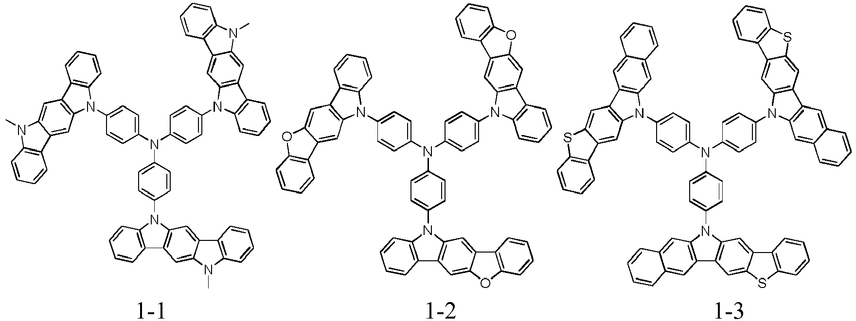


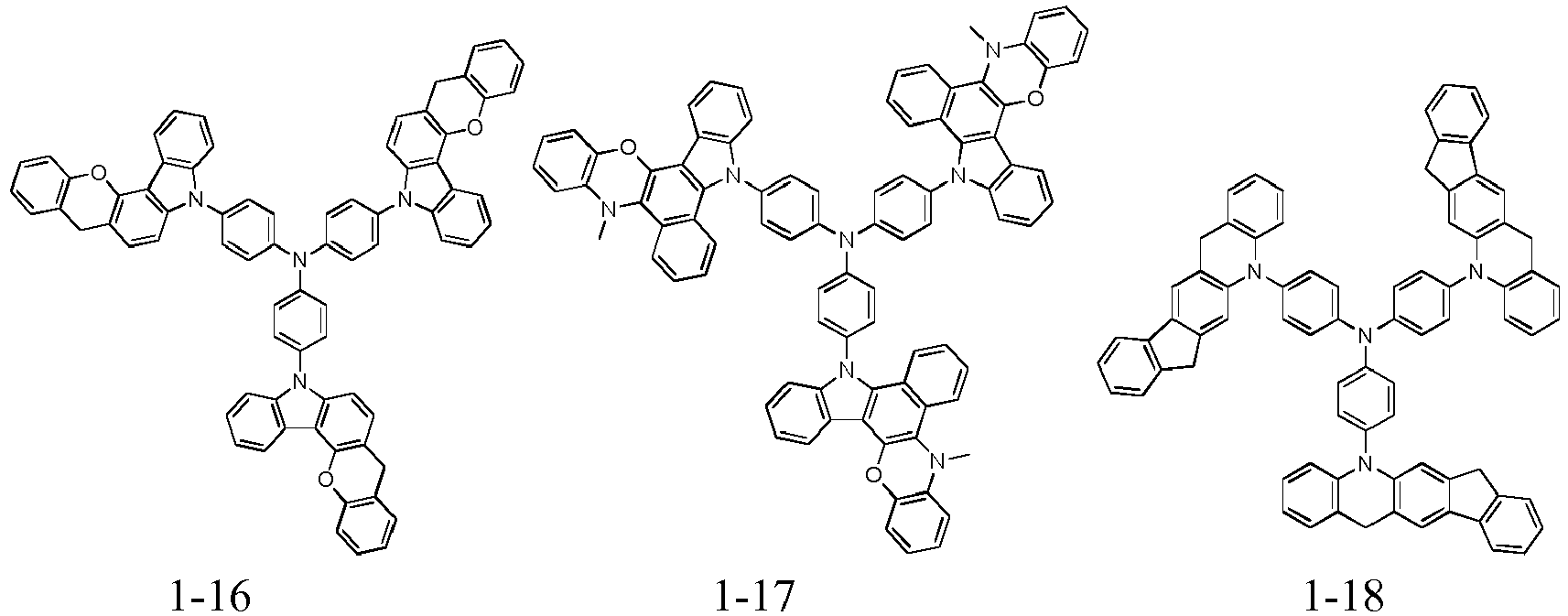


- The organic electroluminescent device according to claim 9, wherein the acceptor host material is a compound with the following structures:


- A manufacturing method for an organic electroluminescent device, comprising:disposing an anode on a substrate;disposing a light-emitting layer on the anode, a host material of the light-emitting layer being formed by premixing a donor host material and an acceptor host material, the donor host material and the acceptor host material being co-evaporated in a same evaporation source to form an exciplex, and the host material is doped with a guest material; anddisposing a cathode on the light-emitting layer.
- The manufacturing method for an organic electroluminescent device according to claim 13, further comprising:sequentially stacking a hole injection layer and a hole transport layer between the anode and the light-emitting layer; anddisposing an optical compensation layer between the hole transport layer and the light-emitting layer.
Applications Claiming Priority (2)
| Application Number | Priority Date | Filing Date | Title |
|---|---|---|---|
| CN201710048295.3A CN108336237B (en) | 2017-01-20 | 2017-01-20 | An organic electroluminescent device |
| PCT/CN2018/073380 WO2018133836A1 (en) | 2017-01-20 | 2018-01-19 | Organic electroluminescent device and fabrication method thereof |
Publications (3)
| Publication Number | Publication Date |
|---|---|
| EP3573118A1 true EP3573118A1 (en) | 2019-11-27 |
| EP3573118A4 EP3573118A4 (en) | 2020-01-22 |
| EP3573118B1 EP3573118B1 (en) | 2023-03-29 |
Family
ID=62908838
Family Applications (1)
| Application Number | Title | Priority Date | Filing Date |
|---|---|---|---|
| EP18741504.7A Active EP3573118B1 (en) | 2017-01-20 | 2018-01-19 | Organic electroluminescent device and fabrication method thereof |
Country Status (7)
| Country | Link |
|---|---|
| US (1) | US11158821B2 (en) |
| EP (1) | EP3573118B1 (en) |
| JP (1) | JP6829768B2 (en) |
| KR (1) | KR102254393B1 (en) |
| CN (1) | CN108336237B (en) |
| TW (1) | TWI667360B (en) |
| WO (1) | WO2018133836A1 (en) |
Cited By (2)
| Publication number | Priority date | Publication date | Assignee | Title |
|---|---|---|---|---|
| CN115224208A (en) * | 2021-04-20 | 2022-10-21 | 中国科学院理化技术研究所 | An exciplex-sensitized phosphorescent organic electroluminescent device |
| US12082429B2 (en) | 2018-10-10 | 2024-09-03 | Semiconductor Energy Laboratory Co., Ltd. | Light-emitting device, light-emitting apparatus, electronic device, and lighting device |
Families Citing this family (14)
| Publication number | Priority date | Publication date | Assignee | Title |
|---|---|---|---|---|
| CN110582854B (en) * | 2016-12-02 | 2023-03-14 | 纽约州州立大学研究基金会 | Method for manufacturing multilayer amorphous selenium sensor for melting |
| KR102495414B1 (en) | 2017-03-08 | 2023-02-02 | 이데미쓰 고산 가부시키가이샤 | Chemical compounds, materials for organic electroluminescent devices, organic electroluminescent devices, and electronic devices |
| KR102637792B1 (en) | 2018-03-22 | 2024-02-19 | 삼성디스플레이 주식회사 | Organic light emitting device and electronic device including the same |
| CN109638170B (en) * | 2018-11-07 | 2021-10-19 | 北京绿人科技有限责任公司 | An organic electro-optical element |
| CN113170549B (en) * | 2018-11-30 | 2024-02-23 | 九州有机光材股份有限公司 | Film manufacturing method, organic semiconductor element manufacturing method, and organic semiconductor element |
| KR102804493B1 (en) | 2019-04-30 | 2025-05-09 | 삼성디스플레이 주식회사 | Organic light emitting device |
| KR102770368B1 (en) * | 2020-03-03 | 2025-02-18 | 주식회사 엘지화학 | Novel compound and organic light emitting device comprising the same |
| CN111943829B (en) * | 2020-07-27 | 2022-04-15 | 清华大学 | Exciplex, application thereof and organic electroluminescent device adopting exciplex |
| KR20220085924A (en) | 2020-12-15 | 2022-06-23 | 삼성디스플레이 주식회사 | Light emitting device and electronic apparatus comprising same |
| CN114639786B (en) * | 2020-12-15 | 2025-08-22 | 云谷(固安)科技有限公司 | Light-emitting device and display panel |
| CN112979623B (en) * | 2021-02-22 | 2022-09-09 | 吉林奥来德光电材料股份有限公司 | A five-membered heterocyclic compound and preparation method thereof, organic electroluminescent device and element |
| CN113969168B (en) * | 2021-10-27 | 2024-06-21 | 京东方科技集团股份有限公司 | Red light organic electroluminescent composition, red light organic electroluminescent device and display device containing the same |
| KR20250074833A (en) * | 2023-11-20 | 2025-05-28 | 에스에프씨 주식회사 | Novel Heterocyclic compounds and Organic light emitting diode including the same |
| CN119661546A (en) * | 2025-02-24 | 2025-03-21 | 西安欧得光电材料有限公司 | Organic light-emitting compound and organic electroluminescent device thereof |
Family Cites Families (20)
| Publication number | Priority date | Publication date | Assignee | Title |
|---|---|---|---|---|
| CN1303083C (en) * | 2003-02-12 | 2007-03-07 | 昱镭光电科技股份有限公司 | Red organic electroluminescent material |
| CN1638585A (en) * | 2003-12-26 | 2005-07-13 | 日东电工株式会社 | Electroluminescence device, planar light source and display using the same |
| JP5646733B2 (en) * | 2010-04-28 | 2014-12-24 | ユニバーサル ディスプレイ コーポレイション | Premixed material deposition |
| JP5694019B2 (en) * | 2011-03-17 | 2015-04-01 | 株式会社東芝 | Organic electroluminescent element, display device and lighting device |
| DE112012007312B4 (en) | 2011-03-23 | 2025-08-07 | Semiconductor Energy Laboratory Co., Ltd. | Light-emitting element |
| KR101932563B1 (en) * | 2012-06-27 | 2018-12-28 | 삼성디스플레이 주식회사 | Organic light-emitting device comprising multi-layered hole transporting layer, and organic light-emitting display apparatus including the same |
| JP2014187130A (en) * | 2013-03-22 | 2014-10-02 | Nippon Hoso Kyokai <Nhk> | Organic electroluminescent element, display device and illuminating device, evaluation method of hole transport material |
| KR102074031B1 (en) * | 2013-09-17 | 2020-02-05 | 가부시키가이샤 큐럭스 | Organic electroluminescence element |
| CN104600213A (en) * | 2013-10-30 | 2015-05-06 | 海洋王照明科技股份有限公司 | Preparation method of organic electroluminescent device |
| US20160322585A1 (en) * | 2014-03-10 | 2016-11-03 | Samsung Sdi Co., Ltd. | Condensed cyclic compound and organic light emitting device including the same |
| KR20160143678A (en) * | 2014-04-22 | 2016-12-14 | 유니버셜 디스플레이 코포레이션 | Material for phosphorescent light-emitting element |
| CN103985822B (en) * | 2014-05-30 | 2017-05-10 | 广州华睿光电材料有限公司 | Organic mixture, composite containing organic mixture, organic electronic device and application |
| KR102377360B1 (en) * | 2014-08-08 | 2022-03-21 | 가부시키가이샤 한도오따이 에네루기 켄큐쇼 | Light-emitting element, light-emitting device, lighting device, display device, display panel, and electronic appliance |
| TWI666803B (en) * | 2014-09-17 | 2019-07-21 | 日商日鐵化學材料股份有限公司 | Organic electric field light emitting element and manufacturing method thereof |
| CN104538559B (en) * | 2014-12-31 | 2017-10-10 | 北京维信诺科技有限公司 | A kind of organic electroluminescence display device and method of manufacturing same with rgb pixel area |
| CN105895811B (en) * | 2015-01-26 | 2018-03-20 | 北京维信诺科技有限公司 | A kind of thermal activation sensitized fluorescence organic electroluminescence device |
| TWI814143B (en) * | 2015-03-09 | 2023-09-01 | 日商半導體能源研究所股份有限公司 | Light-emitting element, display device, electronic device, and lighting device |
| US20180254426A1 (en) * | 2015-03-30 | 2018-09-06 | Nippon Steel & Sumikin Chemical Co., Ltd. | Organic electroluminescent element |
| CN106328816B (en) * | 2015-06-16 | 2018-11-13 | 昆山国显光电有限公司 | A kind of organic electroluminescence device and preparation method thereof |
| KR20250105465A (en) * | 2015-07-08 | 2025-07-08 | 가부시키가이샤 한도오따이 에네루기 켄큐쇼 | Light-emitting element, display device, electronic device, and lighting device |
-
2017
- 2017-01-20 CN CN201710048295.3A patent/CN108336237B/en active Active
-
2018
- 2018-01-19 EP EP18741504.7A patent/EP3573118B1/en active Active
- 2018-01-19 KR KR1020197015666A patent/KR102254393B1/en active Active
- 2018-01-19 JP JP2019529234A patent/JP6829768B2/en active Active
- 2018-01-19 WO PCT/CN2018/073380 patent/WO2018133836A1/en not_active Ceased
- 2018-01-19 TW TW107101972A patent/TWI667360B/en active
-
2019
- 2019-01-11 US US16/317,491 patent/US11158821B2/en active Active
Cited By (2)
| Publication number | Priority date | Publication date | Assignee | Title |
|---|---|---|---|---|
| US12082429B2 (en) | 2018-10-10 | 2024-09-03 | Semiconductor Energy Laboratory Co., Ltd. | Light-emitting device, light-emitting apparatus, electronic device, and lighting device |
| CN115224208A (en) * | 2021-04-20 | 2022-10-21 | 中国科学院理化技术研究所 | An exciplex-sensitized phosphorescent organic electroluminescent device |
Also Published As
| Publication number | Publication date |
|---|---|
| US11158821B2 (en) | 2021-10-26 |
| CN108336237B (en) | 2020-01-31 |
| KR20190069584A (en) | 2019-06-19 |
| US20190165286A1 (en) | 2019-05-30 |
| WO2018133836A1 (en) | 2018-07-26 |
| TWI667360B (en) | 2019-08-01 |
| EP3573118A4 (en) | 2020-01-22 |
| CN108336237A (en) | 2018-07-27 |
| JP6829768B2 (en) | 2021-02-10 |
| TW201827628A (en) | 2018-08-01 |
| KR102254393B1 (en) | 2021-05-24 |
| EP3573118B1 (en) | 2023-03-29 |
| JP2020513691A (en) | 2020-05-14 |
Similar Documents
| Publication | Publication Date | Title |
|---|---|---|
| EP3573118B1 (en) | Organic electroluminescent device and fabrication method thereof | |
| EP3618132B1 (en) | Organic electroluminescent element | |
| EP3950880B1 (en) | Melt mixture for organic electroluminescent element, and organic electroluminescent element | |
| WO2021114751A1 (en) | Organic electroluminescent device, display panel and display device | |
| JP2024028704A (en) | organic electroluminescent device | |
| CN107078221A (en) | Organic electroluminescence element | |
| EP3605634B1 (en) | Organic electroluminescent element | |
| EP4083033B1 (en) | Organic electroluminescent element | |
| JP2012530369A (en) | Phenanthroazole compounds as hole transport materials for electroluminescent devices | |
| EP3399566B1 (en) | Organic electroluminescence element | |
| KR20180020577A (en) | Novel compound and organic electroluminescent device comprising the same | |
| CN110783462B (en) | Electronic device, display device, method for producing the same, and compound | |
| WO2019039174A1 (en) | Host material, film and organic light-emitting element | |
| US20260082760A1 (en) | Luminescent material, and organic electroluminescent element | |
| KR102580610B1 (en) | Organic electroluminescent device comprising polycyclic compounds | |
| KR102499365B1 (en) | Organic electroluminescent device comprising polycyclic aromatic hydrocarbons and manufacturing method thereof | |
| KR102849729B1 (en) | Compositions and organic light-emitting devices | |
| KR20100133352A (en) | Organic photoelectric device | |
| CN111433927B (en) | Compound for electron transport layer and organic electroluminescent element containing the same | |
| CN116635395A (en) | Organic electroluminescence element | |
| KR101198861B1 (en) | Cyanostilbene based Organic Electroluminescent Compound and Organic Electroluminescent Device Using the Same | |
| JP2026046735A (en) | Boron-containing compounds, light-emitting materials, organic electroluminescent elements, and electronic devices | |
| KR102044135B1 (en) | Phosphorescent compound and Organic light emitting diode device using the same |
Legal Events
| Date | Code | Title | Description |
|---|---|---|---|
| STAA | Information on the status of an ep patent application or granted ep patent |
Free format text: STATUS: THE INTERNATIONAL PUBLICATION HAS BEEN MADE |
|
| PUAI | Public reference made under article 153(3) epc to a published international application that has entered the european phase |
Free format text: ORIGINAL CODE: 0009012 |
|
| STAA | Information on the status of an ep patent application or granted ep patent |
Free format text: STATUS: REQUEST FOR EXAMINATION WAS MADE |
|
| 17P | Request for examination filed |
Effective date: 20190531 |
|
| AK | Designated contracting states |
Kind code of ref document: A1 Designated state(s): AL AT BE BG CH CY CZ DE DK EE ES FI FR GB GR HR HU IE IS IT LI LT LU LV MC MK MT NL NO PL PT RO RS SE SI SK SM TR |
|
| AX | Request for extension of the european patent |
Extension state: BA ME |
|
| A4 | Supplementary search report drawn up and despatched |
Effective date: 20200103 |
|
| RIC1 | Information provided on ipc code assigned before grant |
Ipc: H01L 51/52 20060101ALI20191218BHEP Ipc: C07C 13/00 20060101ALI20191218BHEP Ipc: H01L 51/54 20060101ALI20191218BHEP Ipc: H01L 51/50 20060101AFI20191218BHEP Ipc: C07D 333/10 20060101ALI20191218BHEP |
|
| DAV | Request for validation of the european patent (deleted) | ||
| DAX | Request for extension of the european patent (deleted) | ||
| STAA | Information on the status of an ep patent application or granted ep patent |
Free format text: STATUS: EXAMINATION IS IN PROGRESS |
|
| 17Q | First examination report despatched |
Effective date: 20211021 |
|
| REG | Reference to a national code |
Ref country code: DE Ref legal event code: R079 Ref document number: 602018047760 Country of ref document: DE Free format text: PREVIOUS MAIN CLASS: H01L0051500000 Ipc: H01L0051540000 |
|
| RIC1 | Information provided on ipc code assigned before grant |
Ipc: C07D 333/10 20060101ALI20221118BHEP Ipc: C07C 13/00 20060101ALI20221118BHEP Ipc: H01L 51/54 20060101AFI20221118BHEP |
|
| GRAP | Despatch of communication of intention to grant a patent |
Free format text: ORIGINAL CODE: EPIDOSNIGR1 |
|
| STAA | Information on the status of an ep patent application or granted ep patent |
Free format text: STATUS: GRANT OF PATENT IS INTENDED |
|
| INTG | Intention to grant announced |
Effective date: 20230109 |
|
| GRAS | Grant fee paid |
Free format text: ORIGINAL CODE: EPIDOSNIGR3 |
|
| GRAA | (expected) grant |
Free format text: ORIGINAL CODE: 0009210 |
|
| STAA | Information on the status of an ep patent application or granted ep patent |
Free format text: STATUS: THE PATENT HAS BEEN GRANTED |
|
| AK | Designated contracting states |
Kind code of ref document: B1 Designated state(s): AL AT BE BG CH CY CZ DE DK EE ES FI FR GB GR HR HU IE IS IT LI LT LU LV MC MK MT NL NO PL PT RO RS SE SI SK SM TR |
|
| REG | Reference to a national code |
Ref country code: CH Ref legal event code: EP |
|
| REG | Reference to a national code |
Ref country code: DE Ref legal event code: R096 Ref document number: 602018047760 Country of ref document: DE |
|
| REG | Reference to a national code |
Ref country code: AT Ref legal event code: REF Ref document number: 1557276 Country of ref document: AT Kind code of ref document: T Effective date: 20230415 |
|
| REG | Reference to a national code |
Ref country code: IE Ref legal event code: FG4D |
|
| P01 | Opt-out of the competence of the unified patent court (upc) registered |
Effective date: 20230526 |
|
| REG | Reference to a national code |
Ref country code: LT Ref legal event code: MG9D |
|
| PG25 | Lapsed in a contracting state [announced via postgrant information from national office to epo] |
Ref country code: RS Free format text: LAPSE BECAUSE OF FAILURE TO SUBMIT A TRANSLATION OF THE DESCRIPTION OR TO PAY THE FEE WITHIN THE PRESCRIBED TIME-LIMIT Effective date: 20230329 Ref country code: NO Free format text: LAPSE BECAUSE OF FAILURE TO SUBMIT A TRANSLATION OF THE DESCRIPTION OR TO PAY THE FEE WITHIN THE PRESCRIBED TIME-LIMIT Effective date: 20230629 Ref country code: LV Free format text: LAPSE BECAUSE OF FAILURE TO SUBMIT A TRANSLATION OF THE DESCRIPTION OR TO PAY THE FEE WITHIN THE PRESCRIBED TIME-LIMIT Effective date: 20230329 Ref country code: LT Free format text: LAPSE BECAUSE OF FAILURE TO SUBMIT A TRANSLATION OF THE DESCRIPTION OR TO PAY THE FEE WITHIN THE PRESCRIBED TIME-LIMIT Effective date: 20230329 Ref country code: HR Free format text: LAPSE BECAUSE OF FAILURE TO SUBMIT A TRANSLATION OF THE DESCRIPTION OR TO PAY THE FEE WITHIN THE PRESCRIBED TIME-LIMIT Effective date: 20230329 |
|
| REG | Reference to a national code |
Ref country code: NL Ref legal event code: MP Effective date: 20230329 |
|
| REG | Reference to a national code |
Ref country code: AT Ref legal event code: MK05 Ref document number: 1557276 Country of ref document: AT Kind code of ref document: T Effective date: 20230329 |
|
| PG25 | Lapsed in a contracting state [announced via postgrant information from national office to epo] |
Ref country code: SE Free format text: LAPSE BECAUSE OF FAILURE TO SUBMIT A TRANSLATION OF THE DESCRIPTION OR TO PAY THE FEE WITHIN THE PRESCRIBED TIME-LIMIT Effective date: 20230329 Ref country code: NL Free format text: LAPSE BECAUSE OF FAILURE TO SUBMIT A TRANSLATION OF THE DESCRIPTION OR TO PAY THE FEE WITHIN THE PRESCRIBED TIME-LIMIT Effective date: 20230329 Ref country code: GR Free format text: LAPSE BECAUSE OF FAILURE TO SUBMIT A TRANSLATION OF THE DESCRIPTION OR TO PAY THE FEE WITHIN THE PRESCRIBED TIME-LIMIT Effective date: 20230630 Ref country code: FI Free format text: LAPSE BECAUSE OF FAILURE TO SUBMIT A TRANSLATION OF THE DESCRIPTION OR TO PAY THE FEE WITHIN THE PRESCRIBED TIME-LIMIT Effective date: 20230329 |
|
| PG25 | Lapsed in a contracting state [announced via postgrant information from national office to epo] |
Ref country code: SM Free format text: LAPSE BECAUSE OF FAILURE TO SUBMIT A TRANSLATION OF THE DESCRIPTION OR TO PAY THE FEE WITHIN THE PRESCRIBED TIME-LIMIT Effective date: 20230329 Ref country code: RO Free format text: LAPSE BECAUSE OF FAILURE TO SUBMIT A TRANSLATION OF THE DESCRIPTION OR TO PAY THE FEE WITHIN THE PRESCRIBED TIME-LIMIT Effective date: 20230329 Ref country code: PT Free format text: LAPSE BECAUSE OF FAILURE TO SUBMIT A TRANSLATION OF THE DESCRIPTION OR TO PAY THE FEE WITHIN THE PRESCRIBED TIME-LIMIT Effective date: 20230731 Ref country code: ES Free format text: LAPSE BECAUSE OF FAILURE TO SUBMIT A TRANSLATION OF THE DESCRIPTION OR TO PAY THE FEE WITHIN THE PRESCRIBED TIME-LIMIT Effective date: 20230329 Ref country code: EE Free format text: LAPSE BECAUSE OF FAILURE TO SUBMIT A TRANSLATION OF THE DESCRIPTION OR TO PAY THE FEE WITHIN THE PRESCRIBED TIME-LIMIT Effective date: 20230329 Ref country code: AT Free format text: LAPSE BECAUSE OF FAILURE TO SUBMIT A TRANSLATION OF THE DESCRIPTION OR TO PAY THE FEE WITHIN THE PRESCRIBED TIME-LIMIT Effective date: 20230329 |
|
| PG25 | Lapsed in a contracting state [announced via postgrant information from national office to epo] |
Ref country code: SK Free format text: LAPSE BECAUSE OF FAILURE TO SUBMIT A TRANSLATION OF THE DESCRIPTION OR TO PAY THE FEE WITHIN THE PRESCRIBED TIME-LIMIT Effective date: 20230329 Ref country code: PL Free format text: LAPSE BECAUSE OF FAILURE TO SUBMIT A TRANSLATION OF THE DESCRIPTION OR TO PAY THE FEE WITHIN THE PRESCRIBED TIME-LIMIT Effective date: 20230329 Ref country code: IS Free format text: LAPSE BECAUSE OF FAILURE TO SUBMIT A TRANSLATION OF THE DESCRIPTION OR TO PAY THE FEE WITHIN THE PRESCRIBED TIME-LIMIT Effective date: 20230729 |
|
| REG | Reference to a national code |
Ref country code: DE Ref legal event code: R097 Ref document number: 602018047760 Country of ref document: DE |
|
| PG25 | Lapsed in a contracting state [announced via postgrant information from national office to epo] |
Ref country code: DK Free format text: LAPSE BECAUSE OF FAILURE TO SUBMIT A TRANSLATION OF THE DESCRIPTION OR TO PAY THE FEE WITHIN THE PRESCRIBED TIME-LIMIT Effective date: 20230329 Ref country code: CZ Free format text: LAPSE BECAUSE OF FAILURE TO SUBMIT A TRANSLATION OF THE DESCRIPTION OR TO PAY THE FEE WITHIN THE PRESCRIBED TIME-LIMIT Effective date: 20230329 |
|
| PLBE | No opposition filed within time limit |
Free format text: ORIGINAL CODE: 0009261 |
|
| STAA | Information on the status of an ep patent application or granted ep patent |
Free format text: STATUS: NO OPPOSITION FILED WITHIN TIME LIMIT |
|
| 26N | No opposition filed |
Effective date: 20240103 |
|
| PG25 | Lapsed in a contracting state [announced via postgrant information from national office to epo] |
Ref country code: SI Free format text: LAPSE BECAUSE OF FAILURE TO SUBMIT A TRANSLATION OF THE DESCRIPTION OR TO PAY THE FEE WITHIN THE PRESCRIBED TIME-LIMIT Effective date: 20230329 |
|
| PG25 | Lapsed in a contracting state [announced via postgrant information from national office to epo] |
Ref country code: SI Free format text: LAPSE BECAUSE OF FAILURE TO SUBMIT A TRANSLATION OF THE DESCRIPTION OR TO PAY THE FEE WITHIN THE PRESCRIBED TIME-LIMIT Effective date: 20230329 Ref country code: IT Free format text: LAPSE BECAUSE OF FAILURE TO SUBMIT A TRANSLATION OF THE DESCRIPTION OR TO PAY THE FEE WITHIN THE PRESCRIBED TIME-LIMIT Effective date: 20230329 |
|
| PG25 | Lapsed in a contracting state [announced via postgrant information from national office to epo] |
Ref country code: MC Free format text: LAPSE BECAUSE OF FAILURE TO SUBMIT A TRANSLATION OF THE DESCRIPTION OR TO PAY THE FEE WITHIN THE PRESCRIBED TIME-LIMIT Effective date: 20230329 |
|
| PG25 | Lapsed in a contracting state [announced via postgrant information from national office to epo] |
Ref country code: MC Free format text: LAPSE BECAUSE OF FAILURE TO SUBMIT A TRANSLATION OF THE DESCRIPTION OR TO PAY THE FEE WITHIN THE PRESCRIBED TIME-LIMIT Effective date: 20230329 |
|
| REG | Reference to a national code |
Ref country code: CH Ref legal event code: PL |
|
| PG25 | Lapsed in a contracting state [announced via postgrant information from national office to epo] |
Ref country code: LU Free format text: LAPSE BECAUSE OF NON-PAYMENT OF DUE FEES Effective date: 20240119 |
|
| PG25 | Lapsed in a contracting state [announced via postgrant information from national office to epo] |
Ref country code: LU Free format text: LAPSE BECAUSE OF NON-PAYMENT OF DUE FEES Effective date: 20240119 |
|
| PG25 | Lapsed in a contracting state [announced via postgrant information from national office to epo] |
Ref country code: BE Free format text: LAPSE BECAUSE OF NON-PAYMENT OF DUE FEES Effective date: 20240131 |
|
| PG25 | Lapsed in a contracting state [announced via postgrant information from national office to epo] |
Ref country code: CH Free format text: LAPSE BECAUSE OF NON-PAYMENT OF DUE FEES Effective date: 20240131 |
|
| PG25 | Lapsed in a contracting state [announced via postgrant information from national office to epo] |
Ref country code: CH Free format text: LAPSE BECAUSE OF NON-PAYMENT OF DUE FEES Effective date: 20240131 Ref country code: BE Free format text: LAPSE BECAUSE OF NON-PAYMENT OF DUE FEES Effective date: 20240131 |
|
| REG | Reference to a national code |
Ref country code: BE Ref legal event code: MM Effective date: 20240131 |
|
| PG25 | Lapsed in a contracting state [announced via postgrant information from national office to epo] |
Ref country code: BG Free format text: LAPSE BECAUSE OF FAILURE TO SUBMIT A TRANSLATION OF THE DESCRIPTION OR TO PAY THE FEE WITHIN THE PRESCRIBED TIME-LIMIT Effective date: 20230329 |
|
| PG25 | Lapsed in a contracting state [announced via postgrant information from national office to epo] |
Ref country code: BG Free format text: LAPSE BECAUSE OF FAILURE TO SUBMIT A TRANSLATION OF THE DESCRIPTION OR TO PAY THE FEE WITHIN THE PRESCRIBED TIME-LIMIT Effective date: 20230329 |
|
| PG25 | Lapsed in a contracting state [announced via postgrant information from national office to epo] |
Ref country code: IE Free format text: LAPSE BECAUSE OF NON-PAYMENT OF DUE FEES Effective date: 20240119 |
|
| PG25 | Lapsed in a contracting state [announced via postgrant information from national office to epo] |
Ref country code: IE Free format text: LAPSE BECAUSE OF NON-PAYMENT OF DUE FEES Effective date: 20240119 |
|
| PG25 | Lapsed in a contracting state [announced via postgrant information from national office to epo] |
Ref country code: CY Free format text: LAPSE BECAUSE OF FAILURE TO SUBMIT A TRANSLATION OF THE DESCRIPTION OR TO PAY THE FEE WITHIN THE PRESCRIBED TIME-LIMIT; INVALID AB INITIO Effective date: 20180119 |
|
| PG25 | Lapsed in a contracting state [announced via postgrant information from national office to epo] |
Ref country code: HU Free format text: LAPSE BECAUSE OF FAILURE TO SUBMIT A TRANSLATION OF THE DESCRIPTION OR TO PAY THE FEE WITHIN THE PRESCRIBED TIME-LIMIT; INVALID AB INITIO Effective date: 20180119 |
|
| PG25 | Lapsed in a contracting state [announced via postgrant information from national office to epo] |
Ref country code: TR Free format text: LAPSE BECAUSE OF FAILURE TO SUBMIT A TRANSLATION OF THE DESCRIPTION OR TO PAY THE FEE WITHIN THE PRESCRIBED TIME-LIMIT Effective date: 20230329 |
|
| PGFP | Annual fee paid to national office [announced via postgrant information from national office to epo] |
Ref country code: GB Payment date: 20260127 Year of fee payment: 9 |
|
| PGFP | Annual fee paid to national office [announced via postgrant information from national office to epo] |
Ref country code: DE Payment date: 20260114 Year of fee payment: 9 |
|
| PGFP | Annual fee paid to national office [announced via postgrant information from national office to epo] |
Ref country code: FR Payment date: 20260128 Year of fee payment: 9 |