EP3573090A1 - Semiconductor wafer cleaning method - Google Patents
Semiconductor wafer cleaning method Download PDFInfo
- Publication number
- EP3573090A1 EP3573090A1 EP17892697.8A EP17892697A EP3573090A1 EP 3573090 A1 EP3573090 A1 EP 3573090A1 EP 17892697 A EP17892697 A EP 17892697A EP 3573090 A1 EP3573090 A1 EP 3573090A1
- Authority
- EP
- European Patent Office
- Prior art keywords
- oxide film
- semiconductor wafer
- cleaning
- rpm
- rotational speed
- Prior art date
- Legal status (The legal status is an assumption and is not a legal conclusion. Google has not performed a legal analysis and makes no representation as to the accuracy of the status listed.)
- Granted
Links
Images


Classifications
-
- H—ELECTRICITY
- H10—SEMICONDUCTOR DEVICES; ELECTRIC SOLID-STATE DEVICES NOT OTHERWISE PROVIDED FOR
- H10P—GENERIC PROCESSES OR APPARATUS FOR THE MANUFACTURE OR TREATMENT OF DEVICES COVERED BY CLASS H10
- H10P70/00—Cleaning of wafers, substrates or parts of devices
- H10P70/10—Cleaning before device manufacture, i.e. Begin-Of-Line process
- H10P70/15—Cleaning before device manufacture, i.e. Begin-Of-Line process by wet cleaning only
-
- H—ELECTRICITY
- H10—SEMICONDUCTOR DEVICES; ELECTRIC SOLID-STATE DEVICES NOT OTHERWISE PROVIDED FOR
- H10P—GENERIC PROCESSES OR APPARATUS FOR THE MANUFACTURE OR TREATMENT OF DEVICES COVERED BY CLASS H10
- H10P70/00—Cleaning of wafers, substrates or parts of devices
- H10P70/20—Cleaning during device manufacture
-
- H—ELECTRICITY
- H10—SEMICONDUCTOR DEVICES; ELECTRIC SOLID-STATE DEVICES NOT OTHERWISE PROVIDED FOR
- H10P—GENERIC PROCESSES OR APPARATUS FOR THE MANUFACTURE OR TREATMENT OF DEVICES COVERED BY CLASS H10
- H10P72/00—Handling or holding of wafers, substrates or devices during manufacture or treatment thereof
- H10P72/04—Apparatus for manufacture or treatment
- H10P72/0402—Apparatus for fluid treatment
- H10P72/0406—Apparatus for fluid treatment for cleaning followed by drying, rinsing, stripping, blasting or the like
- H10P72/0411—Apparatus for fluid treatment for cleaning followed by drying, rinsing, stripping, blasting or the like for wet cleaning or washing
-
- H—ELECTRICITY
- H10—SEMICONDUCTOR DEVICES; ELECTRIC SOLID-STATE DEVICES NOT OTHERWISE PROVIDED FOR
- H10P—GENERIC PROCESSES OR APPARATUS FOR THE MANUFACTURE OR TREATMENT OF DEVICES COVERED BY CLASS H10
- H10P72/00—Handling or holding of wafers, substrates or devices during manufacture or treatment thereof
- H10P72/70—Handling or holding of wafers, substrates or devices during manufacture or treatment thereof for supporting or gripping
- H10P72/76—Handling or holding of wafers, substrates or devices during manufacture or treatment thereof for supporting or gripping using mechanical means, e.g. clamps or pinches
- H10P72/7604—Handling or holding of wafers, substrates or devices during manufacture or treatment thereof for supporting or gripping using mechanical means, e.g. clamps or pinches the wafers being placed on a susceptor, stage or support
- H10P72/7618—Handling or holding of wafers, substrates or devices during manufacture or treatment thereof for supporting or gripping using mechanical means, e.g. clamps or pinches the wafers being placed on a susceptor, stage or support characterised by a movable susceptor, stage or support, others than those only rotating on their own vertical axis, e.g. susceptors on a rotating carrousel
Definitions
- the present invention relates to a method for cleaning a semiconductor wafer.
- a cleaning solution such as hydrofluoric acid (HF) from the semiconductor wafer (Patent Document 1) .
- FIG. 7 shows a graph illustrating the rotational speed of a semiconductor wafer in a conventional semiconductor-wafer cleaning process (cleaning with ozone water ⁇ pure water ⁇ hydrofluoric acid treatment ⁇ pure water ⁇ ozone water) and drying process.
- the rotation number during the hydrofluoric acid treatment is basically constant, and the rotation number is not changed.
- the rotation number is set constant, for example, at 300 rpm or more, to surely distribute the chemical solution to the outer peripheral portion of a wafer.
- a hydrofluoric acid treatment at such a high speed is completed, if pure water- or ozone water-treatment, drying, and so forth are performed, micro particles and a water mark which resembles a water-flow pattern are increased, bringing about a problem that the wafer quality greatly deteriorates.
- the oxide film is removed by the HF treatment at a constant rotational speed of 100 rpm or less, for example, the solution remains at the wafer outer periphery, resulting in a problem that haze occurs locally.
- Patent Document 1 Japanese Unexamined Patent publication (Kokai) No. 2009-272411
- the conventional method for cleaning a semiconductor wafer has caused the phenomena that surface roughness deteriorates, and that surface defects such as water mark and micro particles are increased.
- An object of the present invention is to provide a method for cleaning a semiconductor wafer by which surface roughness deterioration and surface defect generation can be suppressed.
- the present invention provides a method for cleaning a semiconductor wafer, comprising:
- Such a method for cleaning a semiconductor wafer makes it possible to suppress surface roughness deterioration and suppress surface defect generation.
- the semiconductor wafer is a silicon wafer
- the cleaning solution capable of removing the oxide film is hydrofluoric acid
- the inventive method for cleaning a semiconductor wafer is particularly effective in such a case.
- the oxide film removal at the rotational speed of 300 rpm or more is preferably performed before 90% of the oxide film formed on the surface of the semiconductor wafer is removed, and then the rotational speed of the semiconductor wafer is changed to 100 rpm or less to completely remove the oxide film.
- Removing the oxide film in this manner can more reliably suppress surface roughness deterioration and suppress surface defect generation.
- the oxide film removal at the rotational speed of 300 rpm or more is preferably performed before the semiconductor wafer having the oxide film formed thereon has a contact angle of more than 5° with pure water, and then the rotational speed of the semiconductor wafer is changed to 100 rpm or less to completely remove the oxide film.
- Removing the oxide film in this manner can more reliably suppress surface roughness deterioration and suppress surface defect generation.
- cleaning with pure water or ozone water is preferably performed at the rotational speed of 100 rpm or less.
- the oxide film can be a native oxide film.
- the inventive method for cleaning a semiconductor wafer is particularly suitably utilizable when the oxide film is a native oxide film.
- the inventive method for cleaning a semiconductor wafer makes it possible to suppress surface roughness deterioration and surface defect generation, and obtain a high-quality semiconductor wafer.
- the conventional method for cleaning a semiconductor wafer has problems that a localized haze abnormality occurs, and that surface defects such as water mark and micro particles are increased.
- the present inventors have found that when an oxide film of a wafer is removed using a single-wafer-processing spin dryer, high speed rotation is required to keep the surface roughness, and low speed rotation is required to suppress the particles and water mark.
- the inventors have found that after the water-repelling surface of a wafer is exposed, cleaning at high speed rotation facilitates repelling of the chemical solution, thereby increasing the particles and water mark.
- the present inventors have earnestly studied to achieve the object and consequently discovered that when the oxide film is removed by a high speed rotation at 300 rpm or more so as to keep the haze level before the water-repelling surface is attained and then the processing proceeds to a low speed rotation at 100 rpm or less to completely remove the oxide film, it is possible to suppress surface roughness deterioration and suppress surface defect generation.
- the present invention provides a method for cleaning a semiconductor wafer, including:
- a target to be cleaned is a semiconductor wafer having a surface with an oxide film formed thereon.
- the kind of the semiconductor wafer is not particularly limited, and an example thereof includes a silicon wafer.
- the oxide film includes a native oxide film, a thermal oxide film, and the like, and a native oxide film (e.g., the film thickness: 0.5 nm to 1.5 nm) is preferable.
- the native oxide film can be formed, for example, by cleaning with ozone water (e.g., ozone concentration: 3 ppm or more) or pure water.
- Such a semiconductor wafer whose surface has an oxide film formed thereon is supplied with a cleaning solution capable of removing the oxide film, and cleaned, while the semiconductor wafer is being rotated, to remove the oxide film formed on the surface of the semiconductor wafer.
- the present invention is characterized in that this oxide film removal is performed such that a rotational speed of the semiconductor wafer is 300 rpm or more after the cleaning with the cleaning solution is started and before a water-repelling surface is attained, and then the rotational speed of the semiconductor wafer is changed to 100 rpm or less to completely remove the oxide film.
- Such a method for cleaning a semiconductor wafer can suppress surface roughness deterioration and surface defect generation.
- the cleaning solution capable of removing the oxide film is preferably hydrofluoric acid (e.g., 0.5 to 5.0 wt%).
- the high speed rotation of 300 rpm or more makes it possible to keep the surface roughness, and suppress haze abnormality at the wafer outer periphery.
- the rotational speed is less than 300 rpm, the haze level deteriorates.
- the upper limit of rotational speed is not particularly limited, and can be, for example, 5000 rpm or less.
- the rotational speed of the semiconductor wafer is changed to 100 rpm or less (preferably 50 rpm or less) to completely remove the oxide film. Thereby, generations of surface defects such as particles and water mark can be suppressed. If the high speed rotation of 300 rpm or more is performed in the state of water-repelling surface, or if the changed rotational speed exceeds 100 rpm, surface defect generations such as particles and water mark cannot be suppressed.
- the lower limit of the changed rotational speed is not particularly limited, and is preferably at least several rotations to obtain the cleaning effect.
- the inventive method for cleaning a semiconductor wafer can be carried out as shown in FIG. 1 ; specifically, cleaning is performed with ozone water and pure water to form an oxide film; next, after cleaning with a cleaning solution (HF) capable of removing the oxide film is started and before the water-repelling surface is attained (particularly, immediately before the water-repelling surface is attained), the oxide film removal is performed with a first rotation number of 300 rpm or more; then, the rotation is shifted to a second rotation number of 100 rpm or less to completely remove the oxide film.
- T indicates a timing at which "the water-repelling surface is attained.”
- the state of "water-repelling surface” can be defined using a contact angle of a semiconductor wafer, which has an oxide film formed thereon, with pure water.
- FIGs. 2 (a) to (c) show graphs each illustrating changes in the contact angle of a semiconductor wafer, which has an oxide film formed thereon, with pure water and the percentage of the oxide film removed in the oxide film removal process using hydrofluoric acid (0.2%, 1.0%, 4.0%).
- the contact angles shown in FIGs. 2 (a) to (c) are 5° or less (i.e., hydrophilic surface) for a while after the cleaning is started, but is thereafter rapidly increased, so that a water-repelling surface is obtained.
- the timing at which "the water-repelling surface is attained” in the present invention can be defined as a timing at which the contact angle between a semiconductor wafer, which has an oxide film formed thereon, and pure water exceeds 5°.
- the contact angle can be measured by using a portable contact angle meter PCA-11 manufactured by Kyowa Interface Science Co., Ltd.
- surface roughness deterioration and surface defect generation can be more reliably suppressed by the method in which the oxide film removal at the rotational speed of 300 rpm or more is performed before the semiconductor wafer having the oxide film formed thereon has a contact angle of more than 5° with pure water, and then the rotational speed of the semiconductor wafer is changed to 100 rpm or less to completely remove the oxide film.
- the wafer when the percentage of the oxide film removed is 90% or more, the wafer has a contact angle of more than 5° and has a water-repelling surface.
- the present invention can also provide the method in which the oxide film removal at the rotational speed of 300 rpm or more is performed before 90% of the oxide film formed on the surface of the semiconductor wafer is removed, and then the rotational speed of the semiconductor wafer is changed to 100 rpm or less to completely remove the oxide film.
- the oxide film removal at the rotational speed of 300 rpm or more is preferably performed for the possible longest period before the water-repelling surface is attained.
- the oxide film removal is preferably performed immediately before 90% of the oxide film formed on the surface of the semiconductor wafer is removed, and the oxide film removal can be performed until 80% or more of the oxide film is removed.
- FIG. 3 shows a relation between the time to remove a native oxide film (time to completely separate the oxide film and time to attain the water-repelling surface) and the hydrofluoric acid concentration.
- the time to completely separate the native oxide film time required to remove 100% of the native oxide film
- the percentage of the oxide film removed reaches 90% (i.e., the water-repelling surface is attained) at 25.2 seconds.
- the present invention can provide the method in which the oxide film removal by the high speed rotation at 300 rpm or more is performed before 25.2 seconds elapse after the cleaning with hydrofluoric acid is started, and then the rotation is switched to the low speed rotation at 100 rpm or less.
- cleaning with pure water or ozone water (e.g., 3 ppm or more) is preferably performed to prevent the surface from contamination.
- cleaning with pure water or ozone water is preferably performed at the rotational speed of 100 rpm or less (particularly preferably 50 rpm or less).
- the cleaning with pure water or ozone water by the low speed rotation after the oxide film removal as described above can more reliably suppress generations of water mark, micro particles, etc.
- the rotational speed after the oxide film formation by, for example, the cleaning with pure water or ozone water is not particularly limited, and may be high speed rotation at 300 rpm or more. After that, a drying process is preferably performed.
- Tables 1, 2 show the results of the number of surface defects, ⁇ Haze (haze deterioration amount), and the presence or absence of haze abnormality in the dried semiconductor wafers.
- FIG. 4 shows graphs of (A) the number of defects, given that the value in Example 1 was taken as 100, and (B) the haze deterioration amount, given that the value in Example 1 was taken as 100.
- FIG. 5 shows surface defect maps of the dried semiconductor wafers.
- FIG. 6 shows haze maps after the drying in Comparative Example 1 and Comparative Example 7. It was revealed that Comparative Example 1 had a haze abnormality but Comparative Example 7 had no haze abnormality.
- Example 1 Example 2
- Example 3 Example 4
- Number of defects 747 566 346 300 232 Defect level good good good good good good ⁇ Haze 1.13 ppb 1.04 ppb 1.07 ppb 1.12 ppb 0.98 ppb
- FIG. 6 shows a haze map in Example 6.
- Example 6 was revealed to have no haze abnormality.
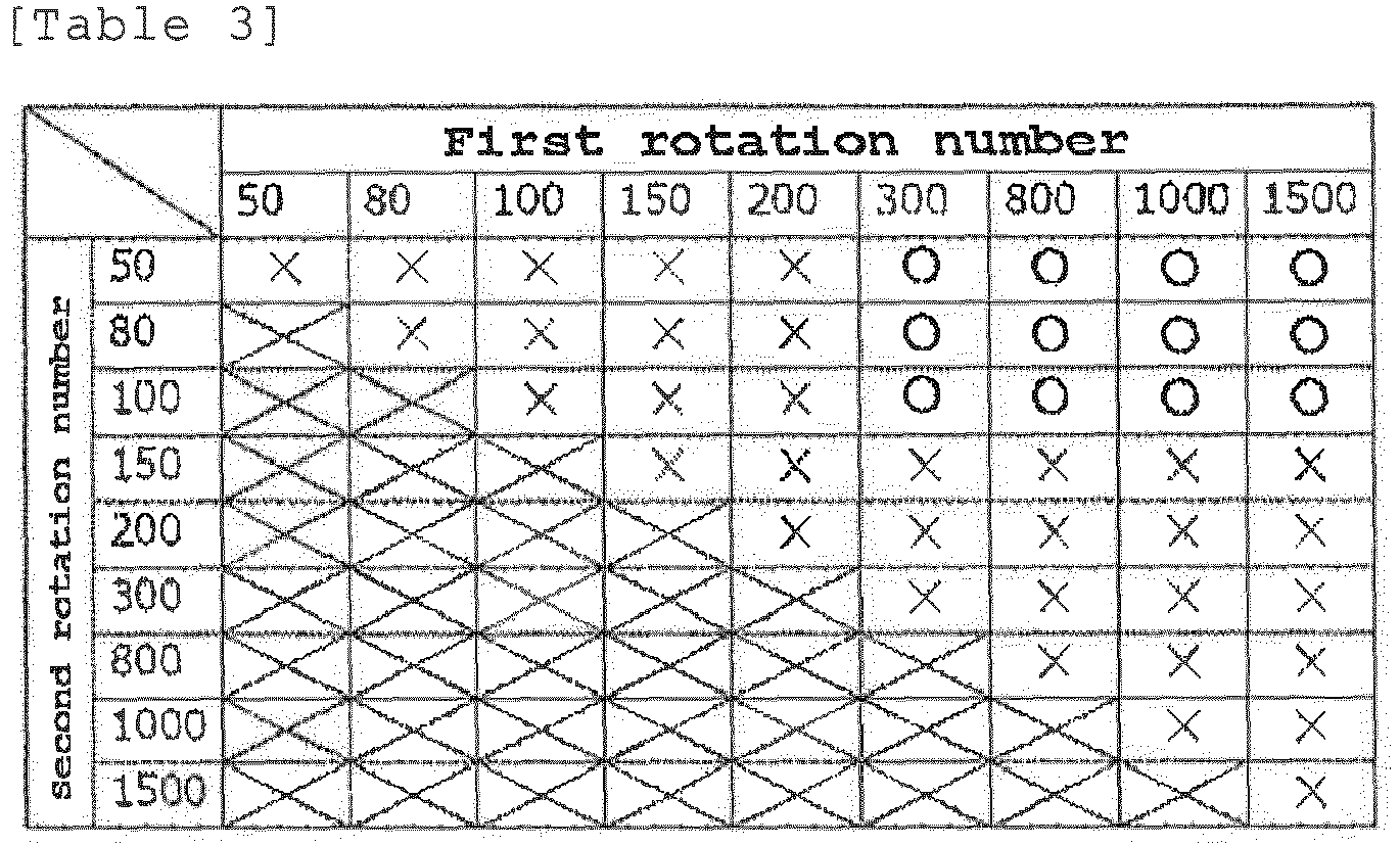
- Table 3 summaries the above results and the results of cleaning and drying under the conditions shown in Table 3 (first rotation number, second rotation number).
- o indicates that a favorable number of defects, a favorable haze deterioration amount, and no haze abnormality; and ⁇ indicates the other states.
- a semiconductor wafer having a diameter of 300 mm was cleaned and dried in the order of ozone water (300 rpm) ⁇ pure water (300 rpm) ⁇ hydrofluoric acid (300 rpm) ⁇ hydrofluoric acid (100 rpm) ⁇ pure water (100 rpm) ⁇ ozone (100 rpm) ⁇ ozone water (100 rpm) ⁇ drying (100 rpm).
- the hydrofluoric acid concentration was 1.0%
- the cleaning with hydrofluoric acid at 300 rpm was performed until about 90% of the oxide film was removed, and then the rotation number was changed to 100 rpm to thus completely remove the oxide film.
- the wafer had a contact angle of 57° with pure water and had a water-repelling surface.
- Comparative Example 13 the number of surface defects was 1121, and the relative value was 150, given that the value in Example 1 was taken as 100; ⁇ Haze was 1.07 ppb, and the relative value was 95, given that the value in Example 1 was taken as 100. It was revealed that surface defects such as water mark and particles were increased by the oxide film removal treatment by the high speed rotation at 300 rpm or more after the water-repelling surface was attained.
Landscapes
- Cleaning Or Drying Semiconductors (AREA)
- Weting (AREA)
Abstract
Description
- The present invention relates to a method for cleaning a semiconductor wafer.
- In a water-repelling surface treatment for a semiconductor wafer (e.g., silicon wafer) by using a single-wafer-processing spin dryer, an oxide film formed on the surface of a semiconductor wafer is generally removed with a cleaning solution such as hydrofluoric acid (HF) from the semiconductor wafer (Patent Document 1) .
-
FIG. 7 shows a graph illustrating the rotational speed of a semiconductor wafer in a conventional semiconductor-wafer cleaning process (cleaning with ozone water → pure water → hydrofluoric acid treatment → pure water → ozone water) and drying process. As shown inFIG. 7 , in the conventional method, the rotation number during the hydrofluoric acid treatment is basically constant, and the rotation number is not changed. - Generally, after the hydrofluoric acid treatment is completed, pure water is used to replace hydrofluoric acid, and ozone water is used to form an oxide film again. Nevertheless, when such a treatment with pure water or ozone water is performed also, the rotation number is basically constant and is not different from that during the hydrofluoric acid treatment.
- Conventionally, when a single-wafer-processing spin dryer is employed as described above, the rotation number is set constant, for example, at 300 rpm or more, to surely distribute the chemical solution to the outer peripheral portion of a wafer. However, after a hydrofluoric acid treatment at such a high speed is completed, if pure water- or ozone water-treatment, drying, and so forth are performed, micro particles and a water mark which resembles a water-flow pattern are increased, bringing about a problem that the wafer quality greatly deteriorates.
- Further, although keeping the surface roughness of a wafer is also important, when the oxide film is removed by the HF treatment at a constant rotational speed of 100 rpm or less, for example, the solution remains at the wafer outer periphery, resulting in a problem that haze occurs locally.
- Patent Document 1: Japanese Unexamined Patent publication (Kokai) No.
2009-272411 - As described above, the conventional method for cleaning a semiconductor wafer has caused the phenomena that surface roughness deteriorates, and that surface defects such as water mark and micro particles are increased.
- The present invention has been made in view of the above-described problems. An object of the present invention is to provide a method for cleaning a semiconductor wafer by which surface roughness deterioration and surface defect generation can be suppressed.
- To achieve the object, the present invention provides a method for cleaning a semiconductor wafer, comprising:
- supplying a semiconductor wafer whose surface has an oxide film formed thereon with a cleaning solution capable of removing the oxide film; and
- cleaning, while rotating, the semiconductor wafer to remove the oxide film formed on the surface of the semiconductor wafer, wherein
- the oxide film is removed such that a rotational speed of the semiconductor wafer is 300 rpm or more after the cleaning with the cleaning solution is started and before a water-repelling surface is attained, and
- then the rotational speed of the semiconductor wafer is changed to 100 rpm or less to completely remove the oxide film.
- Such a method for cleaning a semiconductor wafer makes it possible to suppress surface roughness deterioration and suppress surface defect generation.
- Preferably, in this case, the semiconductor wafer is a silicon wafer, and the cleaning solution capable of removing the oxide film is hydrofluoric acid.
- The inventive method for cleaning a semiconductor wafer is particularly effective in such a case.
- Moreover, the oxide film removal at the rotational speed of 300 rpm or more is preferably performed before 90% of the oxide film formed on the surface of the semiconductor wafer is removed, and then the rotational speed of the semiconductor wafer is changed to 100 rpm or less to completely remove the oxide film.
- Removing the oxide film in this manner can more reliably suppress surface roughness deterioration and suppress surface defect generation.
- Further, the oxide film removal at the rotational speed of 300 rpm or more is preferably performed before the semiconductor wafer having the oxide film formed thereon has a contact angle of more than 5° with pure water, and then the rotational speed of the semiconductor wafer is changed to 100 rpm or less to completely remove the oxide film.
- Removing the oxide film in this manner can more reliably suppress surface roughness deterioration and suppress surface defect generation.
- Furthermore, after the oxide film formed on the surface of the semiconductor wafer is completely removed, cleaning with pure water or ozone water is preferably performed at the rotational speed of 100 rpm or less.
- After the oxide film removal, performing cleaning with pure water or ozone water through low speed rotation as described above makes it possible to more reliably suppress generations of surface defects such as water mark and micro particles.
- In addition, the oxide film can be a native oxide film.
- Thus, the inventive method for cleaning a semiconductor wafer is particularly suitably utilizable when the oxide film is a native oxide film.
- The inventive method for cleaning a semiconductor wafer makes it possible to suppress surface roughness deterioration and surface defect generation, and obtain a high-quality semiconductor wafer.
-
-
FIG. 1 is a graph illustrating an example of the rotational speed of a semiconductor wafer in a method for cleaning a semiconductor wafer of the present invention. -
FIG. 2 shows graphs each illustrating changes in the contact angle and the percentage of the oxide film removed in an oxide-film removal process using hydrofluoric acid (0.2%, 1.0%, 4.0%). -
FIG. 3 is a graph illustrating a relation between the time to remove a native oxide film and the hydrofluoric acid concentration. -
FIG. 4 shows (A) the result of measuring the number of surface defects and (B) the result of measuring the haze deterioration amount in Examples and Comparative Examples. -
FIG. 5 shows surface defect maps after drying in Examples and Comparative Examples. -
FIG. 6 shows haze maps after the drying in Example 6, Comparative Example 1, and Comparative Example 7. -
FIG. 7 is a graph illustrating the rotational speed of a semiconductor wafer in a conventional method for cleaning a semiconductor wafer. - As described above, the conventional method for cleaning a semiconductor wafer has problems that a localized haze abnormality occurs, and that surface defects such as water mark and micro particles are increased. Then, the present inventors have found that when an oxide film of a wafer is removed using a single-wafer-processing spin dryer, high speed rotation is required to keep the surface roughness, and low speed rotation is required to suppress the particles and water mark. Moreover, the inventors have found that after the water-repelling surface of a wafer is exposed, cleaning at high speed rotation facilitates repelling of the chemical solution, thereby increasing the particles and water mark.
- Further, the present inventors have earnestly studied to achieve the object and consequently discovered that when the oxide film is removed by a high speed rotation at 300 rpm or more so as to keep the haze level before the water-repelling surface is attained and then the processing proceeds to a low speed rotation at 100 rpm or less to completely remove the oxide film, it is possible to suppress surface roughness deterioration and suppress surface defect generation. These findings have led to the present invention.
- Specifically, the present invention provides a method for cleaning a semiconductor wafer, including:
- supplying a semiconductor wafer whose surface has an oxide film formed thereon with a cleaning solution capable of removing the oxide film; and
- cleaning, while rotating, the semiconductor wafer to remove the oxide film formed on the surface of the semiconductor wafer, where
- the oxide film is removed such that a rotational speed of the semiconductor wafer is 300 rpm or more after the cleaning with the cleaning solution is started and before a water-repelling surface is attained, and
- then the rotational speed of the semiconductor wafer is changed to 100 rpm or less to completely remove the oxide film.
- Hereinafter, the inventive method for cleaning a semiconductor wafer will be described.
- A target to be cleaned is a semiconductor wafer having a surface with an oxide film formed thereon. The kind of the semiconductor wafer is not particularly limited, and an example thereof includes a silicon wafer. Moreover, the oxide film includes a native oxide film, a thermal oxide film, and the like, and a native oxide film (e.g., the film thickness: 0.5 nm to 1.5 nm) is preferable. Note that the native oxide film can be formed, for example, by cleaning with ozone water (e.g., ozone concentration: 3 ppm or more) or pure water.
- Such a semiconductor wafer whose surface has an oxide film formed thereon is supplied with a cleaning solution capable of removing the oxide film, and cleaned, while the semiconductor wafer is being rotated, to remove the oxide film formed on the surface of the semiconductor wafer. The present invention is characterized in that this oxide film removal is performed such that a rotational speed of the semiconductor wafer is 300 rpm or more after the cleaning with the cleaning solution is started and before a water-repelling surface is attained, and then the rotational speed of the semiconductor wafer is changed to 100 rpm or less to completely remove the oxide film.
- Such a method for cleaning a semiconductor wafer can suppress surface roughness deterioration and surface defect generation.
- In cleaning a semiconductor wafer in the present invention, a conventionally-employed single-wafer-processing spin dryer can be used. Moreover, the cleaning solution capable of removing the oxide film is preferably hydrofluoric acid (e.g., 0.5 to 5.0 wt%).
- After the cleaning with the cleaning solution capable of removing the oxide film is started and before the water-repelling surface is attained (particularly, immediately before the water-repelling surface is attained), the high speed rotation of 300 rpm or more (preferably 1000 rpm or more) makes it possible to keep the surface roughness, and suppress haze abnormality at the wafer outer periphery. After the cleaning is started and before the water-repelling surface is attained, if the rotational speed is less than 300 rpm, the haze level deteriorates. After the cleaning is started and before the water-repelling surface is attained, the upper limit of rotational speed is not particularly limited, and can be, for example, 5000 rpm or less.
- After the oxide film is removed by the high speed rotation at 300 rpm or more before the water-repelling surface is attained (particularly, immediately before the water-repelling surface is attained), the rotational speed of the semiconductor wafer is changed to 100 rpm or less (preferably 50 rpm or less) to completely remove the oxide film. Thereby, generations of surface defects such as particles and water mark can be suppressed. If the high speed rotation of 300 rpm or more is performed in the state of water-repelling surface, or if the changed rotational speed exceeds 100 rpm, surface defect generations such as particles and water mark cannot be suppressed. The lower limit of the changed rotational speed is not particularly limited, and is preferably at least several rotations to obtain the cleaning effect.
- The inventive method for cleaning a semiconductor wafer can be carried out as shown in
FIG. 1 ; specifically, cleaning is performed with ozone water and pure water to form an oxide film; next, after cleaning with a cleaning solution (HF) capable of removing the oxide film is started and before the water-repelling surface is attained (particularly, immediately before the water-repelling surface is attained), the oxide film removal is performed with a first rotation number of 300 rpm or more; then, the rotation is shifted to a second rotation number of 100 rpm or less to completely remove the oxide film. InFIG. 1 , T indicates a timing at which "the water-repelling surface is attained." - In the present invention, the state of "water-repelling surface" can be defined using a contact angle of a semiconductor wafer, which has an oxide film formed thereon, with pure water.
FIGs. 2 (a) to (c) show graphs each illustrating changes in the contact angle of a semiconductor wafer, which has an oxide film formed thereon, with pure water and the percentage of the oxide film removed in the oxide film removal process using hydrofluoric acid (0.2%, 1.0%, 4.0%). The contact angles shown inFIGs. 2 (a) to (c) are 5° or less (i.e., hydrophilic surface) for a while after the cleaning is started, but is thereafter rapidly increased, so that a water-repelling surface is obtained. In other words, the timing at which "the water-repelling surface is attained" in the present invention can be defined as a timing at which the contact angle between a semiconductor wafer, which has an oxide film formed thereon, and pure water exceeds 5°. Incidentally, the contact angle can be measured by using a portable contact angle meter PCA-11 manufactured by Kyowa Interface Science Co., Ltd. - Thus, surface roughness deterioration and surface defect generation can be more reliably suppressed by the method in which the oxide film removal at the rotational speed of 300 rpm or more is performed before the semiconductor wafer having the oxide film formed thereon has a contact angle of more than 5° with pure water, and then the rotational speed of the semiconductor wafer is changed to 100 rpm or less to completely remove the oxide film.
- In this respect, as shown in
FIGs. 2 (a) to (c) , when the percentage of the oxide film removed is 90% or more, the wafer has a contact angle of more than 5° and has a water-repelling surface. - Accordingly, the present invention can also provide the method in which the oxide film removal at the rotational speed of 300 rpm or more is performed before 90% of the oxide film formed on the surface of the semiconductor wafer is removed, and then the rotational speed of the semiconductor wafer is changed to 100 rpm or less to completely remove the oxide film.
- In the present invention, to reliably suppress surface roughness deterioration, the oxide film removal at the rotational speed of 300 rpm or more is preferably performed for the possible longest period before the water-repelling surface is attained. Thus, the oxide film removal is preferably performed immediately before 90% of the oxide film formed on the surface of the semiconductor wafer is removed, and the oxide film removal can be performed until 80% or more of the oxide film is removed.
- Further,
FIG. 3 shows a relation between the time to remove a native oxide film (time to completely separate the oxide film and time to attain the water-repelling surface) and the hydrofluoric acid concentration. For example, when the HF concentration is 1.0%, the time to completely separate the native oxide film (time required to remove 100% of the native oxide film) is 28 seconds. Since the native oxide film is removed (etched) at a constant speed, the percentage of the oxide film removed reaches 90% (i.e., the water-repelling surface is attained) at 25.2 seconds. Thus, in this case, the present invention can provide the method in which the oxide film removal by the high speed rotation at 300 rpm or more is performed before 25.2 seconds elapse after the cleaning with hydrofluoric acid is started, and then the rotation is switched to the low speed rotation at 100 rpm or less. - After the oxide film formed on the surface of the semiconductor wafer is completely removed, cleaning with pure water or ozone water (e.g., 3 ppm or more) is preferably performed to prevent the surface from contamination. Such cleaning with pure water or ozone water is preferably performed at the rotational speed of 100 rpm or less (particularly preferably 50 rpm or less). The cleaning with pure water or ozone water by the low speed rotation after the oxide film removal as described above can more reliably suppress generations of water mark, micro particles, etc.
- The rotational speed after the oxide film formation by, for example, the cleaning with pure water or ozone water is not particularly limited, and may be high speed rotation at 300 rpm or more. After that, a drying process is preferably performed.
- Hereinafter, the present invention will be more specifically described with reference to Examples and Comparative Examples. However, the present invention is not limited to these Examples.
- Using a single-wafer-processing spin dryer, semiconductor wafers each having a diameter of 300 mm were cleaned and dried under conditions shown in Table 1 in the order of ozone water (first rotation number) → pure water (first rotation number) → hydrofluoric acid (first rotation number) → hydrofluoric acid (second rotation number) → pure water (second rotation number)→ ozone (second rotation number) → ozone water (1000 rpm) → drying (1000 rpm). Note that the hydrofluoric acid concentration was 1.0%. In Examples 1 to 5 and Comparative Example 9 to 12, the cleaning with hydrofluoric acid with the first rotation number was performed until about 89% of the oxide film was removed, and then the rotation number was changed to the second rotation number to thus completely remove the oxide film. Note that when the hydrofluoric-acid cleaning with the first rotation number was completed, the wafer had a contact angle of 5° with pure water. Meanwhile, in Comparative Examples 1 to 8, the rotational speed was not changed in the oxide film removal process using hydrofluoric acid.
- Tables 1, 2 show the results of the number of surface defects, ΔHaze (haze deterioration amount), and the presence or absence of haze abnormality in the dried semiconductor wafers.
FIG. 4 shows graphs of (A) the number of defects, given that the value in Example 1 was taken as 100, and (B) the haze deterioration amount, given that the value in Example 1 was taken as 100.FIG. 5 shows surface defect maps of the dried semiconductor wafers.FIG. 6 shows haze maps after the drying in Comparative Example 1 and Comparative Example 7. It was revealed that Comparative Example 1 had a haze abnormality but Comparative Example 7 had no haze abnormality.[Table 1] Example 1 Example 2 Example 3 Example 4 Example 5 First rotation number 300 rpm 800 rpm 1000 rpm 1000 rpm 1500 rpm Second rotation number 100 rpm 100 rpm 50 rpm 100 rpm 50 rpm Number of defects 747 566 346 300 232 Defect level good good good good good ΔHaze 1.13 ppb 1.04 ppb 1.07 ppb 1.12 ppb 0.98 ppb Haze level good good good good good Haze abnormality absent absent absent absent absent 

- Cleaning and drying were performed by the same method as in Examples 1 to 5 described above, except that the first rotation number was 1300 rpm and the second rotational speed was 50 rpm (Example 6).
FIG. 6 shows a haze map in Example 6. Example 6 was revealed to have no haze abnormality. - By the spin cleaning at the single constant speed of 100 rpm or less, the haze deterioration amount was large, and haze abnormality occurred at the wafer outer periphery (Comparative Examples 1 to 3). Moreover, by the spin cleaning at the single constant speed of 150 rpm or more, water mark was generated, and the surface defect level deteriorated (Comparative Examples 4 to 8). Further, even when the rotational speed was changed during the oxide film removal using hydrofluoric acid, if the first rotation number was smaller than 300 rpm, the haze deterioration amount was large (Comparative Examples 9, 10); if the second rotation number was faster than 100 rpm, the number of surface defects was larger (Comparative Examples 11, 12). Note that it was revealed that, in Comparative Examples 9, 10, the haze abnormality occurred at the wafer outer periphery, but the abnormality was absent in appearance.
- In contrast, as in Examples 1 to 6, shifting the high speed rotation of 300 rpm or more to the low speed rotation of 100 rpm or less during the oxide film removal treatment using hydrofluoric acid successfully suppressed the haze deterioration amount, and suppressed haze abnormality and surface defect generations such as water mark.
- Table 3 summaries the above results and the results of cleaning and drying under the conditions shown in Table 3 (first rotation number, second rotation number). In Table 3, o indicates that a favorable number of defects, a favorable haze deterioration amount, and no haze abnormality; and × indicates the other states.
- Using a single-wafer-processing spin dryer, a semiconductor wafer having a diameter of 300 mm was cleaned and dried in the order of ozone water (300 rpm) → pure water (300 rpm) → hydrofluoric acid (300 rpm) → hydrofluoric acid (100 rpm) → pure water (100 rpm) → ozone (100 rpm) → ozone water (100 rpm) → drying (100 rpm). Note that the hydrofluoric acid concentration was 1.0%, the cleaning with hydrofluoric acid at 300 rpm was performed until about 90% of the oxide film was removed, and then the rotation number was changed to 100 rpm to thus completely remove the oxide film. Note that when the hydrofluoric acid cleaning with the first rotation number was completed, the wafer had a contact angle of 57° with pure water and had a water-repelling surface.
- As a result, in Comparative Example 13, the number of surface defects was 1121, and the relative value was 150, given that the value in Example 1 was taken as 100; ΔHaze was 1.07 ppb, and the relative value was 95, given that the value in Example 1 was taken as 100. It was revealed that surface defects such as water mark and particles were increased by the oxide film removal treatment by the high speed rotation at 300 rpm or more after the water-repelling surface was attained.
- It should be noted that the present invention is not limited to the above-described embodiments. The embodiments are just examples, and any examples that have substantially the same feature and demonstrate the same functions and effects as those in the technical concept disclosed in claims of the present invention are included in the technical scope of the present invention.
Claims (6)
- A method for cleaning a semiconductor wafer, including:supplying a semiconductor wafer whose surface has an oxide film formed thereon with a cleaning solution capable of removing the oxide film; andcleaning, while rotating, the semiconductor wafer to remove the oxide film formed on the surface of the semiconductor wafer, whereinthe oxide film is removed such that a rotational speed of the semiconductor wafer is 300 rpm or more after the cleaning with the cleaning solution is started and before a water-repelling surface is attained, and then the rotational speed of the semiconductor wafer is changed to 100 rpm or less to completely remove the oxide film.
- The method for cleaning a semiconductor wafer according to claim 1, wherein
the semiconductor wafer is a silicon wafer, and
the cleaning solution capable of removing the oxide film is hydrofluoric acid. - The method for cleaning a semiconductor wafer according to claim 1 or 2, wherein
the oxide film removal at the rotational speed of 300 rpm or more is performed before 90% of the oxide film formed on the surface of the semiconductor wafer is removed, and
then the rotational speed of the semiconductor wafer is changed to 100 rpm or less to completely remove the oxide film. - The method for cleaning a semiconductor wafer according to any one of claims 1 to 3, wherein
the oxide film removal at the rotational speed of 300 rpm or more is performed before the semiconductor wafer having the oxide film formed thereon has a contact angle of more than 5° with pure water, and
then the rotational speed of the semiconductor wafer is changed to 100 rpm or less to completely remove the oxide film. - The method for cleaning a semiconductor wafer according to any one of claims 1 to 4, wherein after the oxide film formed on the surface of the semiconductor wafer is completely removed, cleaning with pure water or ozone water is performed at the rotational speed of 100 rpm or less.
- The method for cleaning a semiconductor wafer according to any one of claims 1 to 5, wherein the oxide film is a native oxide film.
Applications Claiming Priority (2)
| Application Number | Priority Date | Filing Date | Title |
|---|---|---|---|
| JP2017009295A JP6575538B2 (en) | 2017-01-23 | 2017-01-23 | Semiconductor wafer cleaning method |
| PCT/JP2017/045831 WO2018135226A1 (en) | 2017-01-23 | 2017-12-20 | Semiconductor wafer cleaning method |
Publications (3)
| Publication Number | Publication Date |
|---|---|
| EP3573090A1 true EP3573090A1 (en) | 2019-11-27 |
| EP3573090A4 EP3573090A4 (en) | 2020-11-04 |
| EP3573090B1 EP3573090B1 (en) | 2024-05-01 |
Family
ID=62907914
Family Applications (1)
| Application Number | Title | Priority Date | Filing Date |
|---|---|---|---|
| EP17892697.8A Active EP3573090B1 (en) | 2017-01-23 | 2017-12-20 | Semiconductor wafer cleaning method |
Country Status (8)
| Country | Link |
|---|---|
| US (1) | US11094525B2 (en) |
| EP (1) | EP3573090B1 (en) |
| JP (1) | JP6575538B2 (en) |
| KR (1) | KR102509323B1 (en) |
| CN (1) | CN110140197B (en) |
| SG (1) | SG10201913707UA (en) |
| TW (1) | TWI778004B (en) |
| WO (1) | WO2018135226A1 (en) |
Families Citing this family (2)
| Publication number | Priority date | Publication date | Assignee | Title |
|---|---|---|---|---|
| FI128613B (en) * | 2019-06-19 | 2020-08-31 | Comptek Solutions Oy | Optoelectronic device |
| KR20240121053A (en) * | 2023-02-01 | 2024-08-08 | 에스케이실트론 주식회사 | A semiconductor substrate and a method of cleaning a semiconductor substrate |
Family Cites Families (16)
| Publication number | Priority date | Publication date | Assignee | Title |
|---|---|---|---|---|
| JPH069195B2 (en) * | 1989-05-06 | 1994-02-02 | 大日本スクリーン製造株式会社 | Substrate surface treatment method |
| JP2002368067A (en) * | 2001-06-08 | 2002-12-20 | Tokyo Electron Ltd | Rotary substrate processing apparatus and rotary substrate processing method |
| JP4089809B2 (en) * | 2002-03-13 | 2008-05-28 | Sumco Techxiv株式会社 | Equipment for removing oxide film at edge of semiconductor wafer |
| JP2005327936A (en) * | 2004-05-14 | 2005-11-24 | Canon Inc | Cleaning method and manufacturing method of substrate |
| CN100524639C (en) * | 2005-02-07 | 2009-08-05 | 株式会社荏原制作所 | Substrate processing method, substrate processing apparatus and control program |
| JP2007165366A (en) * | 2005-12-09 | 2007-06-28 | Ebara Corp | Substrate processing apparatus and substrate processing method |
| JP4832201B2 (en) * | 2006-07-24 | 2011-12-07 | 大日本スクリーン製造株式会社 | Substrate processing equipment |
| JP2009147038A (en) * | 2007-12-13 | 2009-07-02 | Dainippon Screen Mfg Co Ltd | Substrate processing method |
| JP5317529B2 (en) | 2008-05-02 | 2013-10-16 | Sumco Techxiv株式会社 | Semiconductor wafer processing method and processing apparatus |
| JP2010177543A (en) * | 2009-01-30 | 2010-08-12 | Ebara Corp | Method and apparatus for processing substrate |
| JP5795917B2 (en) * | 2010-09-27 | 2015-10-14 | 株式会社Screenホールディングス | Substrate processing apparatus and substrate processing method |
| JP5061229B2 (en) * | 2010-10-18 | 2012-10-31 | 東京エレクトロン株式会社 | Substrate cleaning apparatus and substrate cleaning method. |
| JP5589968B2 (en) * | 2011-06-17 | 2014-09-17 | 信越半導体株式会社 | Semiconductor wafer cleaning method |
| JP6379400B2 (en) * | 2013-09-26 | 2018-08-29 | 株式会社Screenホールディングス | Substrate processing method and substrate processing apparatus |
| JP6256828B2 (en) * | 2013-10-10 | 2018-01-10 | 株式会社Screenホールディングス | Substrate processing method and substrate processing apparatus |
| JP2015220284A (en) * | 2014-05-15 | 2015-12-07 | 信越半導体株式会社 | Wafer cleaning method |
-
2017
- 2017-01-23 JP JP2017009295A patent/JP6575538B2/en active Active
- 2017-12-20 WO PCT/JP2017/045831 patent/WO2018135226A1/en not_active Ceased
- 2017-12-20 CN CN201780082034.1A patent/CN110140197B/en active Active
- 2017-12-20 KR KR1020197019648A patent/KR102509323B1/en active Active
- 2017-12-20 SG SG10201913707UA patent/SG10201913707UA/en unknown
- 2017-12-20 US US16/471,609 patent/US11094525B2/en active Active
- 2017-12-20 EP EP17892697.8A patent/EP3573090B1/en active Active
-
2018
- 2018-01-05 TW TW107100403A patent/TWI778004B/en active
Also Published As
| Publication number | Publication date |
|---|---|
| SG10201913707UA (en) | 2020-03-30 |
| KR102509323B1 (en) | 2023-03-13 |
| CN110140197A (en) | 2019-08-16 |
| TWI778004B (en) | 2022-09-21 |
| TW201841240A (en) | 2018-11-16 |
| WO2018135226A1 (en) | 2018-07-26 |
| EP3573090B1 (en) | 2024-05-01 |
| EP3573090A4 (en) | 2020-11-04 |
| JP6575538B2 (en) | 2019-09-18 |
| US20200105517A1 (en) | 2020-04-02 |
| JP2018120886A (en) | 2018-08-02 |
| CN110140197B (en) | 2023-04-28 |
| US11094525B2 (en) | 2021-08-17 |
| KR20190105581A (en) | 2019-09-17 |
Similar Documents
| Publication | Publication Date | Title |
|---|---|---|
| CN112673458B (en) | Semiconductor silicon wafer cleaning device and cleaning method | |
| TWI778110B (en) | Cleaning method of silicon wafer | |
| EP3502322B1 (en) | Gaas substrate and production method therefor | |
| EP3573090B1 (en) | Semiconductor wafer cleaning method | |
| TWI872209B (en) | Semiconductor wafer cleaning method | |
| JP2006120819A (en) | Semiconductor wafer manufacturing method and semiconductor wafer | |
| WO2022224583A1 (en) | Wafer cleaning method and cleaning treatment apparatus | |
| TWI460782B (en) | Wafer surface treatment method | |
| US20090071507A1 (en) | Process for cleaning a semiconductor wafer | |
| WO2023120016A1 (en) | Method for cleaning semiconductor wafer and method for producing semiconductor wafer | |
| TWI909266B (en) | Method for cleaning semiconductor wafer, methof for manufacturing semiconductor wafer and semiconductor wafer | |
| US20250201547A1 (en) | Method for cleaning a semiconductor wafer | |
| WO2025099975A1 (en) | Silicon wafer cleaning method | |
| WO2006035865A1 (en) | Semiconductor wafer manufacturing method and semiconductor wafer | |
| KR20260070956A (en) | Method for manufacturing wafer | |
| TW202446496A (en) | Method for cleaning semiconductor wafer | |
| JP2026505084A (en) | Method for cleaning semiconductor wafers | |
| JP2022166590A (en) | Wafer cleaning method | |
| JP2007042889A (en) | Method for suppressing boron contamination on silicon wafer surface |
Legal Events
| Date | Code | Title | Description |
|---|---|---|---|
| STAA | Information on the status of an ep patent application or granted ep patent |
Free format text: STATUS: THE INTERNATIONAL PUBLICATION HAS BEEN MADE |
|
| PUAI | Public reference made under article 153(3) epc to a published international application that has entered the european phase |
Free format text: ORIGINAL CODE: 0009012 |
|
| STAA | Information on the status of an ep patent application or granted ep patent |
Free format text: STATUS: REQUEST FOR EXAMINATION WAS MADE |
|
| 17P | Request for examination filed |
Effective date: 20190709 |
|
| AK | Designated contracting states |
Kind code of ref document: A1 Designated state(s): AL AT BE BG CH CY CZ DE DK EE ES FI FR GB GR HR HU IE IS IT LI LT LU LV MC MK MT NL NO PL PT RO RS SE SI SK SM TR |
|
| AX | Request for extension of the european patent |
Extension state: BA ME |
|
| DAV | Request for validation of the european patent (deleted) | ||
| DAX | Request for extension of the european patent (deleted) | ||
| REG | Reference to a national code |
Ref country code: DE Ref legal event code: R079 Free format text: PREVIOUS MAIN CLASS: H01L0021304000 Ipc: H01L0021306000 Ref country code: DE Ref legal event code: R079 Ref document number: 602017081674 Country of ref document: DE Free format text: PREVIOUS MAIN CLASS: H01L0021304000 Ipc: H01L0021306000 |
|
| A4 | Supplementary search report drawn up and despatched |
Effective date: 20201002 |
|
| RIC1 | Information provided on ipc code assigned before grant |
Ipc: H01L 21/306 20060101AFI20200928BHEP |
|
| STAA | Information on the status of an ep patent application or granted ep patent |
Free format text: STATUS: EXAMINATION IS IN PROGRESS |
|
| 17Q | First examination report despatched |
Effective date: 20230302 |
|
| GRAP | Despatch of communication of intention to grant a patent |
Free format text: ORIGINAL CODE: EPIDOSNIGR1 |
|
| STAA | Information on the status of an ep patent application or granted ep patent |
Free format text: STATUS: GRANT OF PATENT IS INTENDED |
|
| INTG | Intention to grant announced |
Effective date: 20231208 |
|
| GRAS | Grant fee paid |
Free format text: ORIGINAL CODE: EPIDOSNIGR3 |
|
| GRAA | (expected) grant |
Free format text: ORIGINAL CODE: 0009210 |
|
| STAA | Information on the status of an ep patent application or granted ep patent |
Free format text: STATUS: THE PATENT HAS BEEN GRANTED |
|
| AK | Designated contracting states |
Kind code of ref document: B1 Designated state(s): AL AT BE BG CH CY CZ DE DK EE ES FI FR GB GR HR HU IE IS IT LI LT LU LV MC MK MT NL NO PL PT RO RS SE SI SK SM TR |
|
| REG | Reference to a national code |
Ref country code: GB Ref legal event code: FG4D |
|
| REG | Reference to a national code |
Ref country code: CH Ref legal event code: EP |
|
| REG | Reference to a national code |
Ref country code: DE Ref legal event code: R096 Ref document number: 602017081674 Country of ref document: DE |
|
| REG | Reference to a national code |
Ref country code: IE Ref legal event code: FG4D |
|
| REG | Reference to a national code |
Ref country code: LT Ref legal event code: MG9D |
|
| REG | Reference to a national code |
Ref country code: NL Ref legal event code: MP Effective date: 20240501 |
|
| PG25 | Lapsed in a contracting state [announced via postgrant information from national office to epo] |
Ref country code: IS Free format text: LAPSE BECAUSE OF FAILURE TO SUBMIT A TRANSLATION OF THE DESCRIPTION OR TO PAY THE FEE WITHIN THE PRESCRIBED TIME-LIMIT Effective date: 20240901 |
|
| PG25 | Lapsed in a contracting state [announced via postgrant information from national office to epo] |
Ref country code: BG Free format text: LAPSE BECAUSE OF FAILURE TO SUBMIT A TRANSLATION OF THE DESCRIPTION OR TO PAY THE FEE WITHIN THE PRESCRIBED TIME-LIMIT Effective date: 20240501 |
|
| PG25 | Lapsed in a contracting state [announced via postgrant information from national office to epo] |
Ref country code: FI Free format text: LAPSE BECAUSE OF FAILURE TO SUBMIT A TRANSLATION OF THE DESCRIPTION OR TO PAY THE FEE WITHIN THE PRESCRIBED TIME-LIMIT Effective date: 20240501 Ref country code: HR Free format text: LAPSE BECAUSE OF FAILURE TO SUBMIT A TRANSLATION OF THE DESCRIPTION OR TO PAY THE FEE WITHIN THE PRESCRIBED TIME-LIMIT Effective date: 20240501 |
|
| PG25 | Lapsed in a contracting state [announced via postgrant information from national office to epo] |
Ref country code: GR Free format text: LAPSE BECAUSE OF FAILURE TO SUBMIT A TRANSLATION OF THE DESCRIPTION OR TO PAY THE FEE WITHIN THE PRESCRIBED TIME-LIMIT Effective date: 20240802 |
|
| PG25 | Lapsed in a contracting state [announced via postgrant information from national office to epo] |
Ref country code: PT Free format text: LAPSE BECAUSE OF FAILURE TO SUBMIT A TRANSLATION OF THE DESCRIPTION OR TO PAY THE FEE WITHIN THE PRESCRIBED TIME-LIMIT Effective date: 20240902 |
|
| REG | Reference to a national code |
Ref country code: AT Ref legal event code: MK05 Ref document number: 1683589 Country of ref document: AT Kind code of ref document: T Effective date: 20240501 |
|
| PG25 | Lapsed in a contracting state [announced via postgrant information from national office to epo] |
Ref country code: NL Free format text: LAPSE BECAUSE OF FAILURE TO SUBMIT A TRANSLATION OF THE DESCRIPTION OR TO PAY THE FEE WITHIN THE PRESCRIBED TIME-LIMIT Effective date: 20240501 |
|
| PG25 | Lapsed in a contracting state [announced via postgrant information from national office to epo] |
Ref country code: ES Free format text: LAPSE BECAUSE OF FAILURE TO SUBMIT A TRANSLATION OF THE DESCRIPTION OR TO PAY THE FEE WITHIN THE PRESCRIBED TIME-LIMIT Effective date: 20240501 |
|
| PG25 | Lapsed in a contracting state [announced via postgrant information from national office to epo] |
Ref country code: AT Free format text: LAPSE BECAUSE OF FAILURE TO SUBMIT A TRANSLATION OF THE DESCRIPTION OR TO PAY THE FEE WITHIN THE PRESCRIBED TIME-LIMIT Effective date: 20240501 |
|
| PG25 | Lapsed in a contracting state [announced via postgrant information from national office to epo] |
Ref country code: PL Free format text: LAPSE BECAUSE OF FAILURE TO SUBMIT A TRANSLATION OF THE DESCRIPTION OR TO PAY THE FEE WITHIN THE PRESCRIBED TIME-LIMIT Effective date: 20240501 |
|
| PG25 | Lapsed in a contracting state [announced via postgrant information from national office to epo] |
Ref country code: LV Free format text: LAPSE BECAUSE OF FAILURE TO SUBMIT A TRANSLATION OF THE DESCRIPTION OR TO PAY THE FEE WITHIN THE PRESCRIBED TIME-LIMIT Effective date: 20240501 |
|
| PG25 | Lapsed in a contracting state [announced via postgrant information from national office to epo] |
Ref country code: PT Free format text: LAPSE BECAUSE OF FAILURE TO SUBMIT A TRANSLATION OF THE DESCRIPTION OR TO PAY THE FEE WITHIN THE PRESCRIBED TIME-LIMIT Effective date: 20240902 Ref country code: PL Free format text: LAPSE BECAUSE OF FAILURE TO SUBMIT A TRANSLATION OF THE DESCRIPTION OR TO PAY THE FEE WITHIN THE PRESCRIBED TIME-LIMIT Effective date: 20240501 Ref country code: NO Free format text: LAPSE BECAUSE OF FAILURE TO SUBMIT A TRANSLATION OF THE DESCRIPTION OR TO PAY THE FEE WITHIN THE PRESCRIBED TIME-LIMIT Effective date: 20240801 Ref country code: NL Free format text: LAPSE BECAUSE OF FAILURE TO SUBMIT A TRANSLATION OF THE DESCRIPTION OR TO PAY THE FEE WITHIN THE PRESCRIBED TIME-LIMIT Effective date: 20240501 Ref country code: LV Free format text: LAPSE BECAUSE OF FAILURE TO SUBMIT A TRANSLATION OF THE DESCRIPTION OR TO PAY THE FEE WITHIN THE PRESCRIBED TIME-LIMIT Effective date: 20240501 Ref country code: IS Free format text: LAPSE BECAUSE OF FAILURE TO SUBMIT A TRANSLATION OF THE DESCRIPTION OR TO PAY THE FEE WITHIN THE PRESCRIBED TIME-LIMIT Effective date: 20240901 Ref country code: HR Free format text: LAPSE BECAUSE OF FAILURE TO SUBMIT A TRANSLATION OF THE DESCRIPTION OR TO PAY THE FEE WITHIN THE PRESCRIBED TIME-LIMIT Effective date: 20240501 Ref country code: GR Free format text: LAPSE BECAUSE OF FAILURE TO SUBMIT A TRANSLATION OF THE DESCRIPTION OR TO PAY THE FEE WITHIN THE PRESCRIBED TIME-LIMIT Effective date: 20240802 Ref country code: FI Free format text: LAPSE BECAUSE OF FAILURE TO SUBMIT A TRANSLATION OF THE DESCRIPTION OR TO PAY THE FEE WITHIN THE PRESCRIBED TIME-LIMIT Effective date: 20240501 Ref country code: ES Free format text: LAPSE BECAUSE OF FAILURE TO SUBMIT A TRANSLATION OF THE DESCRIPTION OR TO PAY THE FEE WITHIN THE PRESCRIBED TIME-LIMIT Effective date: 20240501 Ref country code: BG Free format text: LAPSE BECAUSE OF FAILURE TO SUBMIT A TRANSLATION OF THE DESCRIPTION OR TO PAY THE FEE WITHIN THE PRESCRIBED TIME-LIMIT Effective date: 20240501 Ref country code: AT Free format text: LAPSE BECAUSE OF FAILURE TO SUBMIT A TRANSLATION OF THE DESCRIPTION OR TO PAY THE FEE WITHIN THE PRESCRIBED TIME-LIMIT Effective date: 20240501 Ref country code: RS Free format text: LAPSE BECAUSE OF FAILURE TO SUBMIT A TRANSLATION OF THE DESCRIPTION OR TO PAY THE FEE WITHIN THE PRESCRIBED TIME-LIMIT Effective date: 20240801 |
|
| PG25 | Lapsed in a contracting state [announced via postgrant information from national office to epo] |
Ref country code: DK Free format text: LAPSE BECAUSE OF FAILURE TO SUBMIT A TRANSLATION OF THE DESCRIPTION OR TO PAY THE FEE WITHIN THE PRESCRIBED TIME-LIMIT Effective date: 20240501 |
|
| PG25 | Lapsed in a contracting state [announced via postgrant information from national office to epo] |
Ref country code: EE Free format text: LAPSE BECAUSE OF FAILURE TO SUBMIT A TRANSLATION OF THE DESCRIPTION OR TO PAY THE FEE WITHIN THE PRESCRIBED TIME-LIMIT Effective date: 20240501 |
|
| PG25 | Lapsed in a contracting state [announced via postgrant information from national office to epo] |
Ref country code: CZ Free format text: LAPSE BECAUSE OF FAILURE TO SUBMIT A TRANSLATION OF THE DESCRIPTION OR TO PAY THE FEE WITHIN THE PRESCRIBED TIME-LIMIT Effective date: 20240501 |
|
| PG25 | Lapsed in a contracting state [announced via postgrant information from national office to epo] |
Ref country code: RO Free format text: LAPSE BECAUSE OF FAILURE TO SUBMIT A TRANSLATION OF THE DESCRIPTION OR TO PAY THE FEE WITHIN THE PRESCRIBED TIME-LIMIT Effective date: 20240501 Ref country code: SK Free format text: LAPSE BECAUSE OF FAILURE TO SUBMIT A TRANSLATION OF THE DESCRIPTION OR TO PAY THE FEE WITHIN THE PRESCRIBED TIME-LIMIT Effective date: 20240501 |
|
| PG25 | Lapsed in a contracting state [announced via postgrant information from national office to epo] |
Ref country code: SM Free format text: LAPSE BECAUSE OF FAILURE TO SUBMIT A TRANSLATION OF THE DESCRIPTION OR TO PAY THE FEE WITHIN THE PRESCRIBED TIME-LIMIT Effective date: 20240501 |
|
| PG25 | Lapsed in a contracting state [announced via postgrant information from national office to epo] |
Ref country code: SM Free format text: LAPSE BECAUSE OF FAILURE TO SUBMIT A TRANSLATION OF THE DESCRIPTION OR TO PAY THE FEE WITHIN THE PRESCRIBED TIME-LIMIT Effective date: 20240501 Ref country code: SK Free format text: LAPSE BECAUSE OF FAILURE TO SUBMIT A TRANSLATION OF THE DESCRIPTION OR TO PAY THE FEE WITHIN THE PRESCRIBED TIME-LIMIT Effective date: 20240501 Ref country code: RO Free format text: LAPSE BECAUSE OF FAILURE TO SUBMIT A TRANSLATION OF THE DESCRIPTION OR TO PAY THE FEE WITHIN THE PRESCRIBED TIME-LIMIT Effective date: 20240501 Ref country code: EE Free format text: LAPSE BECAUSE OF FAILURE TO SUBMIT A TRANSLATION OF THE DESCRIPTION OR TO PAY THE FEE WITHIN THE PRESCRIBED TIME-LIMIT Effective date: 20240501 Ref country code: DK Free format text: LAPSE BECAUSE OF FAILURE TO SUBMIT A TRANSLATION OF THE DESCRIPTION OR TO PAY THE FEE WITHIN THE PRESCRIBED TIME-LIMIT Effective date: 20240501 Ref country code: CZ Free format text: LAPSE BECAUSE OF FAILURE TO SUBMIT A TRANSLATION OF THE DESCRIPTION OR TO PAY THE FEE WITHIN THE PRESCRIBED TIME-LIMIT Effective date: 20240501 |
|
| REG | Reference to a national code |
Ref country code: DE Ref legal event code: R097 Ref document number: 602017081674 Country of ref document: DE |
|
| PG25 | Lapsed in a contracting state [announced via postgrant information from national office to epo] |
Ref country code: IT Free format text: LAPSE BECAUSE OF FAILURE TO SUBMIT A TRANSLATION OF THE DESCRIPTION OR TO PAY THE FEE WITHIN THE PRESCRIBED TIME-LIMIT Effective date: 20240501 |
|
| PLBE | No opposition filed within time limit |
Free format text: ORIGINAL CODE: 0009261 |
|
| STAA | Information on the status of an ep patent application or granted ep patent |
Free format text: STATUS: NO OPPOSITION FILED WITHIN TIME LIMIT |
|
| 26N | No opposition filed |
Effective date: 20250204 |
|
| PG25 | Lapsed in a contracting state [announced via postgrant information from national office to epo] |
Ref country code: SI Free format text: LAPSE BECAUSE OF FAILURE TO SUBMIT A TRANSLATION OF THE DESCRIPTION OR TO PAY THE FEE WITHIN THE PRESCRIBED TIME-LIMIT Effective date: 20240501 |
|
| PG25 | Lapsed in a contracting state [announced via postgrant information from national office to epo] |
Ref country code: MC Free format text: LAPSE BECAUSE OF FAILURE TO SUBMIT A TRANSLATION OF THE DESCRIPTION OR TO PAY THE FEE WITHIN THE PRESCRIBED TIME-LIMIT Effective date: 20240501 |
|
| REG | Reference to a national code |
Ref country code: CH Ref legal event code: PL |
|
| PG25 | Lapsed in a contracting state [announced via postgrant information from national office to epo] |
Ref country code: LU Free format text: LAPSE BECAUSE OF NON-PAYMENT OF DUE FEES Effective date: 20241220 |
|
| GBPC | Gb: european patent ceased through non-payment of renewal fee |
Effective date: 20241220 |
|
| PG25 | Lapsed in a contracting state [announced via postgrant information from national office to epo] |
Ref country code: SE Free format text: LAPSE BECAUSE OF FAILURE TO SUBMIT A TRANSLATION OF THE DESCRIPTION OR TO PAY THE FEE WITHIN THE PRESCRIBED TIME-LIMIT Effective date: 20240501 |
|
| REG | Reference to a national code |
Ref country code: BE Ref legal event code: MM Effective date: 20241231 |
|
| PG25 | Lapsed in a contracting state [announced via postgrant information from national office to epo] |
Ref country code: GB Free format text: LAPSE BECAUSE OF NON-PAYMENT OF DUE FEES Effective date: 20241220 Ref country code: BE Free format text: LAPSE BECAUSE OF NON-PAYMENT OF DUE FEES Effective date: 20241231 |
|
| PG25 | Lapsed in a contracting state [announced via postgrant information from national office to epo] |
Ref country code: CH Free format text: LAPSE BECAUSE OF NON-PAYMENT OF DUE FEES Effective date: 20241231 |
|
| PG25 | Lapsed in a contracting state [announced via postgrant information from national office to epo] |
Ref country code: IE Free format text: LAPSE BECAUSE OF NON-PAYMENT OF DUE FEES Effective date: 20241220 |
|
| REG | Reference to a national code |
Ref country code: DE Ref legal event code: R079 Ref document number: 602017081674 Country of ref document: DE Free format text: PREVIOUS MAIN CLASS: H01L0021306000 Ipc: H10P0050000000 |
|
| PGFP | Annual fee paid to national office [announced via postgrant information from national office to epo] |
Ref country code: DE Payment date: 20251211 Year of fee payment: 9 |
|
| PGFP | Annual fee paid to national office [announced via postgrant information from national office to epo] |
Ref country code: FR Payment date: 20251229 Year of fee payment: 9 |