EP3570462A1 - Coherent optical communication with constellations having electric field coordinates on circles - Google Patents
Coherent optical communication with constellations having electric field coordinates on circles Download PDFInfo
- Publication number
- EP3570462A1 EP3570462A1 EP19173985.3A EP19173985A EP3570462A1 EP 3570462 A1 EP3570462 A1 EP 3570462A1 EP 19173985 A EP19173985 A EP 19173985A EP 3570462 A1 EP3570462 A1 EP 3570462A1
- Authority
- EP
- European Patent Office
- Prior art keywords
- optical
- data
- phase
- electric field
- polarization components
- Prior art date
- Legal status (The legal status is an assumption and is not a legal conclusion. Google has not performed a legal analysis and makes no representation as to the accuracy of the status listed.)
- Granted
Links
- 230000003287 optical effect Effects 0.000 title claims abstract description 322
- 230000005684 electric field Effects 0.000 title claims abstract description 137
- 230000001427 coherent effect Effects 0.000 title claims description 23
- 238000004891 communication Methods 0.000 title description 17
- 230000010287 polarization Effects 0.000 claims abstract description 95
- 238000005259 measurement Methods 0.000 claims abstract description 10
- 239000000203 mixture Substances 0.000 claims abstract description 10
- 239000000969 carrier Substances 0.000 claims description 9
- 239000013307 optical fiber Substances 0.000 description 39
- 238000010276 construction Methods 0.000 description 12
- 230000005540 biological transmission Effects 0.000 description 10
- 230000001902 propagating effect Effects 0.000 description 9
- 238000001514 detection method Methods 0.000 description 7
- 239000000835 fiber Substances 0.000 description 6
- 230000015556 catabolic process Effects 0.000 description 4
- 238000006731 degradation reaction Methods 0.000 description 4
- 230000002123 temporal effect Effects 0.000 description 4
- 239000000654 additive Substances 0.000 description 3
- 230000000996 additive effect Effects 0.000 description 3
- 238000010586 diagram Methods 0.000 description 3
- 239000006185 dispersion Substances 0.000 description 3
- 238000003491 array Methods 0.000 description 2
- 230000006735 deficit Effects 0.000 description 2
- 238000009826 distribution Methods 0.000 description 2
- 230000003993 interaction Effects 0.000 description 2
- 238000000034 method Methods 0.000 description 2
- 239000013598 vector Substances 0.000 description 2
- 229910052691 Erbium Inorganic materials 0.000 description 1
- 238000001069 Raman spectroscopy Methods 0.000 description 1
- 230000003321 amplification Effects 0.000 description 1
- 230000001955 cumulated effect Effects 0.000 description 1
- 230000000694 effects Effects 0.000 description 1
- UYAHIZSMUZPPFV-UHFFFAOYSA-N erbium Chemical compound [Er] UYAHIZSMUZPPFV-UHFFFAOYSA-N 0.000 description 1
- 230000000116 mitigating effect Effects 0.000 description 1
- 238000003199 nucleic acid amplification method Methods 0.000 description 1
- 238000005086 pumping Methods 0.000 description 1
Images


Classifications
-
- H—ELECTRICITY
- H04—ELECTRIC COMMUNICATION TECHNIQUE
- H04B—TRANSMISSION
- H04B10/00—Transmission systems employing electromagnetic waves other than radio-waves, e.g. infrared, visible or ultraviolet light, or employing corpuscular radiation, e.g. quantum communication
- H04B10/25—Arrangements specific to fibre transmission
- H04B10/2507—Arrangements specific to fibre transmission for the reduction or elimination of distortion or dispersion
-
- H—ELECTRICITY
- H04—ELECTRIC COMMUNICATION TECHNIQUE
- H04B—TRANSMISSION
- H04B10/00—Transmission systems employing electromagnetic waves other than radio-waves, e.g. infrared, visible or ultraviolet light, or employing corpuscular radiation, e.g. quantum communication
- H04B10/60—Receivers
- H04B10/61—Coherent receivers
- H04B10/613—Coherent receivers including phase diversity, e.g., having in-phase and quadrature branches, as in QPSK coherent receivers
-
- H—ELECTRICITY
- H04—ELECTRIC COMMUNICATION TECHNIQUE
- H04B—TRANSMISSION
- H04B10/00—Transmission systems employing electromagnetic waves other than radio-waves, e.g. infrared, visible or ultraviolet light, or employing corpuscular radiation, e.g. quantum communication
- H04B10/50—Transmitters
- H04B10/516—Details of coding or modulation
- H04B10/5165—Carrier suppressed; Single sideband; Double sideband or vestigial
-
- H—ELECTRICITY
- H04—ELECTRIC COMMUNICATION TECHNIQUE
- H04B—TRANSMISSION
- H04B10/00—Transmission systems employing electromagnetic waves other than radio-waves, e.g. infrared, visible or ultraviolet light, or employing corpuscular radiation, e.g. quantum communication
- H04B10/60—Receivers
- H04B10/61—Coherent receivers
- H04B10/614—Coherent receivers comprising one or more polarization beam splitters, e.g. polarization multiplexed [PolMux] X-PSK coherent receivers, polarization diversity heterodyne coherent receivers
-
- H—ELECTRICITY
- H04—ELECTRIC COMMUNICATION TECHNIQUE
- H04B—TRANSMISSION
- H04B10/00—Transmission systems employing electromagnetic waves other than radio-waves, e.g. infrared, visible or ultraviolet light, or employing corpuscular radiation, e.g. quantum communication
- H04B10/60—Receivers
- H04B10/61—Coherent receivers
- H04B10/616—Details of the electronic signal processing in coherent optical receivers
- H04B10/6162—Compensation of polarization related effects, e.g., PMD, PDL
-
- H—ELECTRICITY
- H04—ELECTRIC COMMUNICATION TECHNIQUE
- H04B—TRANSMISSION
- H04B10/00—Transmission systems employing electromagnetic waves other than radio-waves, e.g. infrared, visible or ultraviolet light, or employing corpuscular radiation, e.g. quantum communication
- H04B10/60—Receivers
- H04B10/61—Coherent receivers
- H04B10/616—Details of the electronic signal processing in coherent optical receivers
- H04B10/6166—Polarisation demultiplexing, tracking or alignment of orthogonal polarisation components
-
- H—ELECTRICITY
- H04—ELECTRIC COMMUNICATION TECHNIQUE
- H04J—MULTIPLEX COMMUNICATION
- H04J14/00—Optical multiplex systems
- H04J14/06—Polarisation multiplex systems
Definitions
- the invention relates to coherent optical communications.
- the quality of the transmission of information over many types of communication channels typically depends on the constellations of data symbols used to transmit the information in the presence of noise.
- the quality of such transmission of information is also subject to other specific channel impairments, which can be largely compensated. Nevertheless, such constellations and compensation schemes result in the transmission of information constrained by the Shannon limit due to the presence of additive Gaussian white noise (AGWN).
- AGWN additive Gaussian white noise
- AGWN e.g., produced by optical amplifiers
- nonlinear optical distortions produced in optical fibers
- Various embodiments provide apparatus and methods that can mitigation some of the undesired affects caused by additive Gaussian white noise (AGWN) and nonlinear optical distortions to the data symbol stream being optically transmitted.
- AGWN additive Gaussian white noise
- These embodiments are configured for polarization multiplexed, coherent optical communication based on constellations of data symbols whose values may also be less complex to modulate onto optical carriers and/or may also be less complicated to demodulate from such data-modulated optical carriers.
- an apparatus in first embodiments, includes a coherent optical data receiver including two optical hybrids, two light detectors and a digital signal processor (DSP).
- Each optical hybrid outputs mixtures of a corresponding one of the polarization components of a received data-modulated optical carrier with reference light.
- Each light detector outputs digital measurements, at a sequence of times, of the mixtures from a corresponding one of the optical hybrids.
- the digital signal processor is configured to identify a sequence of data symbols of a constellation having parts transmitted on both polarization components of the data-modulated optical carrier in response to receipt of the digital measurements.
- the transmitted data-modulated optical carrier has about a same total light intensity in each optical modulation time slot thereof.
- Each data symbol is defined by in-phase and quadrature-phase electric field coordinates of both polarization components. Pairs of the in-phase and quadrature-phase electric field coordinates of each of the polarization components of the data symbols for each optical modulation time slot are located on a preselected set of two or more concentric circles about an origin.
- the constellation has four times an integer number of dimensions.
- the preselected set may include at least three or at least four of the concentric circles.
- each data symbol may have parts on two or more consecutive ones of the optical modulation time slots.
- the set may include at least three or at least four of the concentric circles.
- the pair of in-phase and quadrature-phase electric field coordinates of the different polarization components of individual ones of the data symbols may be on circles with different size diameters.
- some of the data symbols may have pairs of in-phase and quadrature-phase electric field coordinates the one of the polarization components at adjacent points on one of the circles and also have pairs of in-phase and quadrature-phase electric field coordinates of the other of the polarization components at or near diametrically opposite points on another of the circles of different size diameter.
- the constellation may have data symbols in which a pair of in-phase and quadrature-phase electric field coordinates of the one polarization component is on one of the circles and pairs of in-phase and quadrature-phase electric field coordinates of the other polarization component are at or near diametrically opposite points on another of the circles of different size diameter.
- the first apparatus may further include a coherent optical data transmitter having two in-phase and quadrature-phase optical data modulators and an electronic driver configured to electrically drive said optical data modulators to generate the transmitted data symbols of the constellation.
- a second embodiment of an apparatus includes coherent optical data transmitter.
- the transmitter includes two in-phase and quadrature-phase optical data modulators to modulate an optical carrier, a polarization combiner to combine the modulated optical carriers from the optical data modulators into a polarization multiplexed, data-modulated optical carrier, and an electronic driver connected to electrically drive said optical data modulators according to a constellation for which data symbols have parts transmitted on both polarization components of the data-modulated optical carrier.
- the transmitted data-modulated optical carrier has about a same total light intensity in each optical modulation time slot of the optical data modulators. Pairs of the in-phase and quadrature-phase electric field coordinates of each of the polarization components of the data symbols are located on a preselected set of two or more concentric circles about an origin.
- the constellation has four times an integer number of dimensions.
- the preselected set may include at least three or at least four of the concentric circles.
- each data symbol may have parts on two or more consecutive ones of the optical modulation time slots.
- the preselected set may include at least three or at least four of the concentric circles.
- the pair of in-phase and quadrature-phase electric field coordinates of the different polarization components of individual ones of the data symbols may be on circles with different size diameters.
- some of the data symbols may have pairs of in-phase and quadrature-phase electric field coordinates of one of the polarization components at adjacent points on one of the circles and also have pairs of in-phase and quadrature-phase electric field coordinates of the other of the polarization components at or near diametrically opposite points on another of the circles.
- the constellation may have data symbols in which a pair of in-phase and quadrature-phase electric field coordinates of one of the polarization components is on one of the circles and pairs of in-phase and quadrature-phase electric field coordinates of the other of the polarization components are at or near diametrically opposite points on another of the circles.
- a coherent optical data receiver includes two optical hybrids, two light detectors and a digital signal processor.
- Each optical hybrid is configured to output mixtures of a corresponding one of the polarization components of a received data-modulated optical carrier with reference light.
- Each light detector is configured to output digital measurements of the mixtures at a sequence of times from a corresponding one of the optical hybrids.
- the digital signal processor is configured to identify a sequence of data symbols of a constellation having parts transmitted on both polarization components of the data-modulated optical carrier in response to receipt of the digital measurements.
- the transmitted data-modulated optical carrier has about a same total light intensity in each optical modulation time slot thereof.
- Each data symbol is defined by in-phase and quadrature-phase electric field coordinates of both polarization components.
- the constellation has four times an integer number of dimensions with the integer being greater than one.
- Each data symbol has parts on three or more consecutive ones of the optical modulation time slots.
- some of the data symbols of the constellation may have X-polarization I and Q electric field coordinates and Y-polarization component I and Q electric field coordinates, for at least one optical modulation time slot, located at points of a 3-dimensional sphere about an origin of the electric field coordinates for the at least one optical modulation time slot with the points not located on a preselected set of tori about an origin of the electric field coordinates.
- a coherent optical data transmitter includes two in-phase and quadrature-phase optical data modulators to modulate an optical carrier, a polarization combiner to combine the modulated optical carriers from the optical data modulators into a polarization multiplexed, data-modulated optical carrier, and an electronic driver connected to electrically drive said optical data modulators according to a constellation for which data symbols have parts transmitted on both polarization components of the data-modulated optical carrier.
- the transmitted data-modulated optical carrier has about a same total light intensity in each optical modulation time slot of the optical data modulators.
- the constellation has four times an integer number of dimensions with the integer being greater than one. Each data symbol has parts on three or more consecutive ones of the optical modulation time slots.
- some of the data symbols of the constellation may have X-polarization I and Q electric field coordinates and Y-polarization component I and Q electric field coordinates, for at least one optical modulation time slot, located at points of a 3-dimensional sphere about an origin of the electric field coordinates for the at least one optical modulation time slot with the points not located on a preselected set of tori.
- first and second optical propagating modes of an optical fiber which only significantly differ by having locally orthogonal polarizations, will be referred to as respective first and second orthogonal polarization components of a single optical propagating mode.
- AWGN additive white Gaussian noise
- each data symbol of a constellation will be defined by a set of real electric field coordinate pairs, wherein each electric field coordinate pair, e.g., a pair of in-phase and quadrature-phase electric field values of electric field coordinates, to be located on or near one or more circle(s) about the origin in a relevant 2-dimensional Euclidian space, e.g., the space formed by the in-phase and quadrature phase electric field averaged over an optical modulation time slot.
- Each individual electric field coordinate pair may be constrained to be located on a preselected set of one, two, three, four or more concentric circles about an origin of said 2-dimensional Euclidean space.
- an individual electric field coordinate pair may have values uniformly or non-uniformly distributed on such circle(s).
- the number of available values may be the same or different on different ones of the circles.
- different electric field coordinate pairs of the same data symbol may be jointly constrained, i.e., to limit the values of the different electric field coordinate pairs in the set defining an individual data symbol of the constellation.
- an optical modulation time slot is a time period over which optical data modulator(s) of the optical fiber communication system transmit a single modulation form on an optical carrier.
- the optical modulation time slots typically have temporal lengths given by an inverse of the baud rate for driving the optical data modulator(s).
- the temporal length of a data symbol on the optical carrier may be 1, 2, 3, 4 etc. times the length of the optical modulation time slot.
- some of the geometrically defined constellations of the present application may be advantageous for one or more reasons.
- some such geometrically defined constellations may provide a large minimum Euclidean distance between the data symbols therein even if the minimum distance is not maximized. For this reason, such constellations may still enable the communication of large amounts of information in the presence of AGWN.
- Second, such geometrically defined constellations may provide approximately the same transmitted total optical intensity, when averaged over an optical modulation time slot, e.g., an approximately constant total optical power. Such about constant total transmitted optical power is believed, by the inventors, to reduce undesired non-linear optical degradations of data-modulated optical carrier in the optical transmission fiber(s).
- such geometrically defined embodiments may enable simpler implementations of electronic drivers of optical data modulators in optical data transmitters and/or enable simpler implementations of electronic, data-symbol, demodulator circuits in optical data receivers, e.g., due to simpler algorithms for identifying the electric field coordinate pairs of data symbols, e.g., the pairs of I and Q electric field coordinates of the data symbol.
- FIG. 1 schematically illustrates an optical data transmitter 10.
- the optical data transmitter 10 includes a light source 12; a light splitter 14; a pair of optical data modulators 16, 18; an optical polarization combiner 20; and an electronic driver 22.
- the light source 12 may be a laser, e.g., a continuous-wave output laser, which produces the light for the optical carrier.
- the laser may be a narrow line-width laser, e.g., an external cavity laser.
- the light splitter 14 is connected to receive light from the light source 12 and transmit part of the received light to each of the optical data modulators 16, 18, e.g., in about equal intensity parts.
- the light splitter 14 may be, e.g., a conventional optical intensity splitter, e.g., a 50/50 optical splitter, or may be a conventional polarization beam splitter appropriately aligned with respect to the polarization output of the light source 12, e.g., to produce two about equal intensity light beams.
- the optical data modulators 16, 18 may be conventional optical modulators for phase modulating an optical carrier. Each of the optical data modulators 16, 18 is capable of separately modulating the in-phase (I) and quadrature-phase (Q) components of the optical carrier in response to electrical driving signals from the electronic driver 22.
- each optical data modulator 16,18 may be a nested Mach-Zehnder interferometer (MZI), in which the data-modulated optical carriers produced by the two component MZIs of the nested MZI are combined with a relative phase of about ⁇ /2 radians to produce I and Q data-modulated parts of one polarization component of the final data-modulated optical carrier.
- MZI Mach-Zehnder interferometer
- the optical polarization combiner 20 combines the two components of the data-modulated optical carriers received from the two optical data modulators 16, 18 with different polarizations, e.g., with relatively orthogonal polarizations at the near end face optical fiber transmission line 24. That is, the optical polarization combiner 20 combines the component data-modulated optical carrier from the two optical data modulator 16, 18 to produce a polarization-multiplexed, data-modulated optical carrier incident on near end face the optical fiber line 24.
- optical polarization combiner 20 may perform said combining operation so that the light from each optical data modulator 16, 18 primarily excites a different one of two orthogonal polarization components of a single optical propagating mode of the optical fiber line 24, at the near end face thereof.
- the electronic driver 22 is connected to receive an input digital data stream (DATA) and map segments thereof, e.g., consecutive segments, into corresponding data symbols and to output corresponding electrical signal sets to drive the pair of optical data modulators 16, 18 to modulate the optical carriers to carry the data symbols.
- the electronic driver 22 outputs a temporal sequence of D sets of electrical driver signals for the two optical data modulators 16, 18, via electrical connections (EC) for each of said data symbols, i.e., for D optical modulation time slots.
- D is a positive integer, e.g., 1, 2, 3, 4, etc.
- each consecutive such set causes parallel I and Q modulation by each optical data modulator 16, 18 in a single optical modulation time slot.
- the electronic driver 22 operates the optical data modulators 16, 18 in parallel, e.g., simultaneously, so that portions of each data symbol are modulated onto the two components of the optical carrier by the individual optical data modulators 16, 18.
- first and second separate portions of each data symbol are typically carried by the two relatively orthogonal polarization components of the optical propagating mode in the optical fiber line 24.
- the electronic driver 22 may operate the optical data modulators 16, 18 to modulate portions an individual data symbol onto the optical carrier over one or more optical modulation time slots. That is, the transmission of a single data symbol may require and a temporal sequence of sequential optical modulations on the final optical carrier.
- the optical fiber line 24 supports two orthogonal polarization components of one or more optical propagating mode(s) therein.
- the optical fiber line 24 may include one or more spans of conventional single mode optical fiber or of one or more spans of a multimode optical fiber, e.g., a few mode optical fiber.
- the optical data transmitter 10 may transmit a stream of data symbols by using both orthogonal polarization components of the same lateral spatial propagating mode(s) of the optical fiber line 24. For example, such a pair of orthogonally polarization components of one type of optical propagating mode in a multimode or multicore optical fiber line.
- internal connecting optical paths are schematically indicated by an optical waveguide (OW). But, some or all of said internal connecting optical paths may also be free space optical paths in other embodiments.
- OW optical waveguide
- FIG. 2 schematically illustrates an example of an optical data receiver 30, i.e., a coherent optical data receiver.
- the optical data receiver 30 includes a local optical source 32; a light splitter 34; optical hybrids 36, 38; a polarization splitter 40; analog electronic detection and processing circuits 42, 44; and a digital signal processor 46.
- the local optical source 32 may be, e.g., a continuous-wave laser with about the same wavelength as received data-modulated optical carrier.
- the local optical source 32 may be a narrow line width laser, e.g., an external cavity laser.
- the light splitter 34 receives light from the local optical source 32 and transmits a portion of said light to each of the optical hybrids 36, 38, e.g., about equal intensity portions thereof.
- the light splitter 14 may be, e.g., a conventional optical intensity splitter, e.g., a 50/50 optical splitter, or a conventional polarization beam splitter appropriately aligned with respect to the polarization of the light beam from the local optical source 32.
- Each optical hybrid 36, 38 is an optical mixer that interferes, at optical outputs thereof, combinations of light received at their two optical inputs.
- each optical hybrid 36, 38 may be a conventional 90-degree optical hybrid, for which a difference in optical intensities on one pair of the optical outputs may be a measure of primarily an I-component of the received data-modulated optical carrier, and the difference in the optical intensities on the other pair of optical outputs may be a measure of primarily a Q-component of said same data- modulated optical carrier.
- the optical hybrids 36, 38 may have any conventional construction, e.g., planar waveguide optical mixers or multimode optical interference devices, and a person of ordinary skill would understand how to make suitable ones of such optical hybrids in light of the present disclosure.
- the polarization splitter 40 splits the data-modulated optical carrier, which is received from the optical fiber line 24, into two, about orthogonal, polarization components and transmits each of the polarization components to a corresponding one of the optical hybrids 36, 38.
- each optical hybrid 36, 38 is connected for optical coherent detection of the I-phase and Q-phase modulation of one of the polarization components of a received data-modulated optical carrier.
- Each analog electronic detection and processing circuit 42, 44 detects the optical signals at the optical outputs of a corresponding one of the optical hybrids 36, 38.
- Each analog electronic detection and processing circuit 42, 44 may include one or more balanced arrays of photodiodes for detecting differences in light intensities at pairs of optical outputs of the corresponding optical hybrid 36, 38, low-pass electronic filter(s) for processing electrical signals output by one or more the balanced arrays, electronic amplifiers for amplifying said processed electrical signals, and analog-to-digital converters to convert said amplified electrical signals into digital representations thereof.
- Each analog electronic detection and processing circuit 42, 44 outputs two digital electrical signals indicative of the data-modulations of the two phases, e.g., the I and Q phases, of one polarization component of the data-modulated optical carrier received from the optical fiber line 24.
- the digital signal processor 46 is connected to receive, from the analog electronic detection and processing circuits 42, 44 via electrical connections (EC), a digital signal stream indicative of data modulations on I and Q phases of the two orthogonal polarization components of the data-modulated optical carrier received from the optical fiber line 24.
- the digital signal processor 46 includes circuitry for correcting for various types of optical impairments ins the received data-modulated optical carrier, e.g., cumulated chromatic dispersion, phase and frequency offset, I-Q misalignment, and polarization mode dispersion and polarization rotation.
- the digital signal processor (DSP) 46 is configured to demodulate data symbols of a constellation whose data symbols are defined by modulations of the I and Q phases of the optical carrier in both orthogonal polarization components thereof.
- the modulations defining one data symbol extend over a sequence of D consecutive optical carrier modulation periods, wherein D is a positive integer, e.g., 1, 2, 3, 4, etc. That is, the DSP 46 is configured to identify parallel modulations of the transmitted data-modulated optical carrier over a consecutive sequence of one or more optical modulation time slots, in order to demodulate individual data symbols.
- the DSP 46 outputs a digital data stream (DATA) indicative of the data carried by the stream of data symbols modulated on the data-modulated optical carrier received from the optical fiber line 24.
- DATA digital data stream
- individual internal connecting optical paths are indicated by optical waveguides (OW), but, some or all of said internal connecting optical paths may also be formed as free space optical paths in other embodiments.
- OW optical waveguides
- electrical connections EC connect the analog electronic detection and processing circuits 42, 44 to the DSP 46.
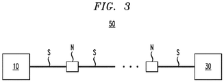
- FIG 3 schematically illustrates an example of an all-optical fiber communication system 50.
- the optical fiber communication system 50 includes the optical data transmitter 10 of Figure 1 , the optical data receiver 30 of Figure 2 , and the optical fiber line 24 of Figures 1 - 2 .
- the optical fiber line 24 may have a sequence of one or more optical fiber spans S, which are optically end-coupled by intermediate nodes (N).
- One or more intermediate nodes (N) may provide conventional optical amplification, e.g., by providing conventional forward and/or backward Raman pumping and/or conventional lumped erbium doped fiber, optical amplifier(s), and/or may provide conventional optical dispersion management.
- Such intermediate optical processing of the transmitted data-modulated optical carrier will introduce AGWN onto the data-modulated optical carrier being communicated from the optical data transmitter 10 to the optical data receiver 30.
- the communication over the optical fiber line 24 may also introduce nonlinear optical degradation into said data-modulated optical carrier.
- the optical fiber line 24 has one or more spans of single mode optical fiber. From the present description, the person of ordinary skill in the relevant arts would understand how to implement the inventions in embodiments where the optical fiber line 24 is formed by spans of multimode fiber, e.g., multicore or few mode optical fiber.
- the constellations could also be implemented with two orthogonal polarization components of an optical propagating mode in embodiments in which the optical fiber line 24 includes spans of multimode optical fiber.
- constellations of various embodiments will be described with respect to the optical data transmitter 10, the optical data receiver 30, and the optical communication system 50 of Figures 1 - 3 .
- the electronic driver 22 and the DSP 46 of Figures 1 -2 will have circuitry for enabling optical data communication via these special constellations of data symbols.
- the constellations are embedded in four or more Euclidean dimensions, e.g., 4D dimensions with D a positive integer, e.g., 1, 2, 3, 4, etc.
- the data symbols of each such constellation lie on or near a corresponding (4D-1)-dimensional sphere, i.e., S 4D-1 .
- the sphere is embedded in a 4D real Euclidean space and is centered on the origin of the Euclidean space.
- the electronic driver 22 typically maintains the total energy of the transmitted data-modulated optical carrier to be approximately constant.
- the average value of the total light intensity over an optical modulation time slot may be approximately constant when said average value is compared for different optical modulation time slots. Due to the approximate constant total light intensity, the inventors believe that undesired effects of nonlinear optical interactions should be reduced.
- the total energy of the transmitted, data-modulated optical carrier may be approximately constant over consecutive optical modulation time slots even in embodiments for which a single data symbol occupies a plurality of consecutive optical modulation time slots.
- the available values of data symbols are on and/or near a corresponding sphere, i.e., S 4D-1 , and are preferably spread over and/or near the sphere in a manner that provides a large minimum distance between the data symbols.
- the data symbols are defined in a manner that may provide simplified algorithms for electrically driving the optical data modulators 16, 18, with the electronic driver 22, and/or for identifying individual ones of the data symbols during data demodulation in the DSP 46.
- An axially symmetric single-mode fiber usually has two optical propagating modes of orthogonal polarization.
- electric field vectors will be referred to as E X ( x , t) and E Y ( x , t), respectively, where x is the spatial position and t is the time.
- E X ( x , t) and E Y ( x , t) are locally orthogonal at all points x.
- 2 i.e., integrated over the optical fiber's cross section.
- nonlinear optical interactions are about proportional to the total light intensity, e.g., about proportional to
- D small number
- R is a constant
- E X,I (t) 2 , E X,Q (t) 2 , E Y,I (t) 2 , and E Y,Q (t) 2 are the averages of squares of the electrical fields of the I-phase and Q-phase components of the X and Y orthogonal polarization components of the modulated optical carrier integrated over the cross section of the optical fiber (csf), and "t" is time of the optical modulation time slot.
- Eq. (1) states that the total light intensity, summed over the optical modulation time slots of the data symbol is constant.
- the total intensity is a sum of intensities of the orthogonal I-phase and Q-phase parts of the data-modulated optical carrier summed over the two X and Y orthogonal polarization components.
- Eq. (1) implies that the data symbols of the constellation lie on a (4D-1)-dimensional sphere about the origin in 4D-dimensional real Euclidean space where the real Euclidean electric field coordinates of a data symbol are: E X , I t 1 , E X , Q t 1 , E Y , I t 1 , E Y , Q t 1 , ... , E X , I t D , E X , Q t D , E Y , I t D , E Y , D t D .
- constructions are given to define the data symbols for different constellations.
- the constructions involve imposing constraints on electric field coordinate pairs, i.e., the above pairs of electric field values or electric field coordinates for the X and Y orthogonal polarizations in a sequence of one or more modulation time slots for a data symbol, of the individual data symbols to be on one, two, or more circles about the origin in the 2-dimensional real Euclidean spaces of the electric field coordinate pairs.
- Such constructions produce sets of data symbols that can be easily defined for modulation and/or easily identified during demodulation, e.g., because the individual electric field coordinate pairs of a data symbol are located on or near a preselected set of one or more concentric circles.
- Equation (1_1 states that the data symbol of an optical modulation time slot "t", is a point on a 3-dimensional sphere of radius R in the real Euclidean space formed by values of the real and imaginary parts of the X and Y electric fields, i.e., the Euclidean space whose points are: ⁇ E X,I (t), E X,Q (t), E Y,I (t), E Y,Q (t) ⁇ .
- Equation (1_1) is one constraint on the 4 real electric field coordinates E X,I (t), E X,Q (t), E Y,I (t), and E Y,Q (t) of each transmitted data symbol.
- E X,I (t) ⁇ E X,I , E X,Q (t) ⁇ E X,Q , E Y,I ⁇ E Y,I , E Y,Q (t) ⁇ E Y,Q for writing simplicity below.
- each data symbol may be subject to further constraints on their defining I and Q electric field coordinate pairs (E X,I , E X,Q ) and (E X,I , E X,Q ).
- (1_1) is solved for the X polarization component, I and Q, electric field coordinate pair (E X,I , E X,Q ) being on a first circle of radius R X and for the Y-polarization component, I and Q, electric field coordinate pair (E Y,I , E Y,Q ) being on a second circle of radius R Y where both circles have centers at (0, 0) in the relevant 2-dimensional Euclidean space.
- each X-polarization, I and Q, electric field coordinate pair (E X,I , E X,Q ) lies on an E X circle of radius R X (1) or R X (2)
- each Y-polarization, I and Q, electric field coordinate pair (E Y,I , E Y,Q ) lies on an E Y circle of radius R Y (1) or R Y (2).
- Electric field coordinate pairs are empty small circles in Figure 4 . To ensure that eq.
- This constraint is schematically illustrated by 2 dashed double arrowed lines between the two circles for the electric field coordinate pair (E X,I , E X,Q ) and the two circles for the electric field coordinate pair (E Y,I , E Y,Q ), i.e., to indicate circle-to-circle constraints.
- the constellation has one data symbol for each pairing of a point of the inner E X circle with a point of the outer E Y circle, and also has one data symbol for each pairing of a point of the outer E X circle with a point of the inner E Y circle.
- the numbers of points on the each of the E X and E Y circles may be different and/or the distributions of said points may be different on the various E X and E Y circles, e.g., being uniformly or non-uniformly distributed on the various E X and E Y circles.
- the electronic driver 22 of Figure 1 and/or the DSP 46 of Figure 2 may be less complex.
- the simple geometrical definitions of the locations of such electric field coordinate pairs of the data symbols may enable less complex algorithms for determining driver values for producing the transmitted data symbols, i.e., during modulation, and/or less complex algorithms for identifying received data symbols, i.e., during demodulation, than in alternate coherent optical communication systems in which data symbols are uniformly distributed over a 3-dimensional sphere.
- the DSP 46 may be simpler and possibly more rapid than a DSP in a coherent optical data receiver for a constellation whose data symbols are more uniformly spatially distributed on a 3-dimensional sphere.
- the present embodiments may not provide the most advantageous constellations with respect to error protection, some such embodiments may enable higher baud rates in the DSP 46 of the coherent optical data receiver 30.
- the constellations impose other constraints between the X-polarization, I and Q, electric field coordinate pairs (E X,I , E X,Q ) and the Y-polarization, I and Q, electric field coordinate pairs (E Y,I , E Y,Q ) of data symbols.
- Dashed double arrowed lines indicate illustrative electric field coordinate pairs (E X,I , E X,Q ) and (E Y,I , E Y,Q ) satisfying the constraints.
- Such pairs are empty small circles in Figures 5 - 7 .
- the other constraints associate points of the E X circles to points of the E Y circles without associating all points of any pair of E x and E Y circles in a data symbol.
- Each illustrated construction has 32 data symbols.
- Other embodiments evident to the person of ordinary skill in light of the present disclosure, can have different numbers of data symbols.
- the further constraints may increase the minimum distance between the data symbols of such constellations and/or may improve the uniformity of the distribution of data symbols of the constellation on a 3-dimensional sphere.
- Figure 5 schematically illustrates a two concentric circle construction of a constellation in which each X-polarization, I and Q, electric field coordinate pair (E X,I , E X,Q ) lies on an inner or outer circle and each Y-polarization, I and Q, electric field coordinate pair (E Y,I , E Y,Q ) lies on an inner or outer circle.
- the electric field coordinate pair (E X,I , E X,Q ) lies on the inner E X circle when the electric field coordinate pair (E Y,I , E Y,Q ) lies on the outer E Y circle
- the electric field coordinate pair (E X,I , E X,Q ) lies on the outer E X circle when the electric field coordinate pair (E Y,I , E Y,Q ) lies on the inner E Y circle.
- the data symbols are defined such that each value of X-polarization, I and Q, electric field coordinate pair (E X,I , E X,Q ) is associated with a single value of the Y-polarization, I and Q, electric field coordinate pair (E Y,I , E Y,Q ).
- the data symbols are defined such that neighboring points on the outer E X circle are associated to about diametrically opposite points on the inner E Y circle and such that neighboring points on the outer E Y circle are associated to about diametrically opposite points on the inner E X circle.
- the minimum distance can be large, because a small distance between one, I and Q, electric field coordinate pair of two data symbols can imply a large distance between the other, I and Q, electric field coordinate pair of said two data symbols.
- Figure 6 schematically illustrates yet another two concentric circle construction of a constellation whose data symbols have X-polarization, I and Q, electric field coordinate pair (E X,I , E X,Q ) on an inner or outer E X circle and Y-polarization, I and Q, electric field coordinate pair (E Y,I , E Y,Q ) on an inner or outer E Y circle.
- the electric field coordinate pair (E X,I , E X,Q ) lies on the inner E X circle when the electric field coordinate pair (E Y,I , E Y,Q ) lies on the outer E Y circle
- the electric field coordinate pair (E X,I , E X,Q ) lies on the outer E X circle when the electric field coordinate pair (E Y,I , E Y,Q ) lies on the inner E Y circle.
- 2 data symbols are defined for each value of an X-polarization, I and Q, electric field coordinate pair on an inner or outer E X circle, because the Y-polarization, I and Q, electric field coordinate pairs can have two diametrically opposite values on the respective outer or inner E Y circle. If the point of the pair (E X,I , E X,Q ) is on the inner E X circle, there are only two data symbols for which the pair (E Y,I , E Y,Q ) has values at or near diametrically opposite points on the outer E Y circle.
- Figure 7 schematically illustrates yet another two concentric circle construction of a constellation whose data symbols have X-polarization, I and Q, electric field coordinate pairs (E X,I , E X,Q ) on an inner or outer E X circle and Y-polarization, I and Q, electric field coordinate pairs (E Y,I , E Y,Q ) on an inner or outer E Y circle.
- the electric field coordinate pair (E X,I , E X,Q ) lies on the inner E X circle when the electric field coordinate pair (E Y,I , E Y,Q ) lies on the outer E Y circle
- the electric field coordinate pair (E X,I , E X,Q ) lies on the outer E X circle when the electric field coordinate pair (E Y,I , E Y,Q ) lies on the inner E Y circle.
- 2 data symbols are defined for each value of an I and Q, electric field coordinate pair on an inner E X or E Y circle, which are associated with two diametrically opposite values on the respective outer E Y or E X circle.
- each data symbol of a constellation extends over a sequence of D consecutive optical modulation time slots as in above eq. (2), i.e., for D > 1.
- the data symbols satisfy eq. (1) so that the total light intensity is about constant, when averaged over the D optical modulation time slots of individual data symbols.
- the data symbols are located on or near points of a (4D-1)-dimensional spheres in a 4D-dimensional real Euclidean space as already discussed.
- the inventors believe that advantageous specific embodiments of such constellations may be further constrained such that the data symbols are on or near points of a space that is a direct product of D 3-dimensional spheres.
- the sequence of D consecutive optical modulation time slots ⁇ t 1 , ..., t D ⁇ is the set of optical modulation time slots of a single data symbol.
- (1_1_1) implies that the total light intensity is constant over individual optical modulation time slots "t r " even though an individual data symbol spans a plurality of such optical modulation time slots.
- the inventors believe that some such special constellations may reduce undesired nonlinear optical degradations of the data symbols during transmission through the optical fiber line 24 while enabling a larger minimum distance between said data symbols, e.g., larger than for some constellations of Figures 4-7 .
- each part of a same data symbol, in the D different optical modulation time slots may be in one of the 4-dimensional constellations of Figures 4 - 7 , but the 4-dimensional constellation of Figures 4 - 7 may be different for the parts of the same data symbol in the D different optical modulation time slots.
- D 2
- the part of some data symbols in the first optical modulation time slot may belong to the constellation of Figure 4
- the part of the same some data symbols in the second optical modulation time slot may belong to a constellation of Figure 5, 6, or 7 .
- constraints may be imposed between parts of an individual data symbol in different optical modulation time slots "t r " of the same data symbol.
- D 2
- the two parts of a single data symbol in consecutive optical modulation time slots may both belong to one of the 4-dimensional constellations of Figures 4 - 7 .
- Said two parts of the same data symbol for part or all of the constellation may be subject to constraint(s) that further restrict the allowed values of ⁇ E X,I (t 1 ), E X,Q (t 1 ) ⁇ according to the values of ⁇ E Y,I (t 2 ), E Y,Q (t 2 ) ⁇ or may alternately further restrict the allowed values of ⁇ E X,I (T 1 ), E X,Q (t 1 ) ⁇ according to the values of ⁇ E X,I (t 2 ), E X,Q (t 2 ) ⁇ .
- the electric field coordinate pairs ⁇ E X,I (t 1 ), E X,Q (t 1 ) ⁇ and ⁇ E Y,I (t 2 ), E Y,Q (t 2 ) ⁇ may be mutually constrained as already described with respect to any of above Figures 4, 5, 6, or 7 except that the electric field coordinate pairs on the E X circles and the E Y circles are in different optical modulation time slots of the same data symbol.
- the electric field coordinate pairs ⁇ E X,I (t 1 ), E X,Q (t 1 ) ⁇ and ⁇ E X,I (t 2 ), E X,Q (t 2 ) ⁇ of the t 1 and t 2 optical modulation time slots may be mutually constrained as described with respect to any of Figures 4, 5, 6, or 7 except that electric field coordinate pairs on the E X circles in Figures 4 - 7 are now on E X (t 1 ) circles and electric field coordinate pairs on the E Y circles in Figures 4 -7 are now on E X (t 2 ) circles.
- Said two parts of the same data symbol may also be subject to constraint(s) that further relate the allowed values of ⁇ E Y,I (t 1 ), E Y,Q (t 1 ) ⁇ to the values of ⁇ E X,I (t 2 ), E X,Q (t 2 ) ⁇ or further relate the allowed values of ⁇ E Y,I (t 1 ), E Y,Q (t 1 ) ⁇ to the values of ⁇ E X,I (t 2 ), E X,Q (t 2 ) ⁇ in analogous manners.
- the electric field coordinate pairs ⁇ E Y,I (t 1 ), E Y,Q (t 1 ) ⁇ and ⁇ E X,I (t 2 ), E X,Q (t 2 ) ⁇ may be mutually constrained as already described with respect to any of above Figures 4, 5, 6, or 7 except that the electric field coordinate pairs on the E Y circles and the E X circles are in different optical modulation time slots of the same data symbol.
- the electric field coordinate pairs ⁇ E Y,I (t 1 ), E Y,Q (t 1 ) ⁇ and ⁇ E Y,I (t 2 ), E Y,Q (t 2 ) ⁇ of the t 1 and t 2 optical modulation time slots may be mutually constrained as described with respect to any of Figures 4, 5, 6, or 7 except that the electric field coordinate pairs on the E X circles in Figures 4 - 7 are on now on E Y (t 1 ) circles and the electric field coordinate pairs on E Y circles in Figures 4 -7 are now on E Y (t 2 ) circles.
- electric field coordinate pairs of each polarization component may be restricted to be on the inner circles of Figure 4, 5, 6, or 7 in all optical modulation time slots "t r " or alternately may be restricted to be on the outer circles of Figure 4, 5, 6, or 7 in all optical modulation time slots "t r ".
- the electric field coordinate pairs ⁇ E Y,I (t r ), E Y,Q (t r ) ⁇ may be restricted to be on the outer circles of Figure 4, 5, 6, or 7 in all optical modulation time slots "t r " or alternately may be restricted to be on the inner circles of Figure 4, 5, 6, or 7 in all optical modulation time slots "t r ".
- Such constraints may reduce undesired degradations of data symbols due to nonlinear optical effects.
- the 4 real electric field coordinates ⁇ E X,I (t r ), E X,Q (t r ), E Y,I (t r ), E Y,Q (t r ) ⁇ of data symbols, for each optical modulation time slot "t r " may be more generally located.
- the set of 4 real electric field coordinates for X-polarization and Y-polarization parts of each data symbol i.e., the sets ⁇ E X,I (t r ), E X,Q (t r ), E Y,I (t r ), E Y,Q (t r ) ⁇ may be constrained to lie on a 3-dimensional sphere of the same radius "R", for one or more optical modulation time slots t r of a data symbol, rather than being constrained to lie on products of sets of concentric circles as already described.
- such constellations may still be useful in some embodiments of the optical data transmitter 10 of Figure 1 , the optical data receiver 30 of Figure, and/or the fiber optical communication system 50 of Figure 3 .
- the transmitted data-modulated optical carrier will still satisfy the requirement of having an about constant total light intensity or energy in each optical modulation time slot.
- Such embodiments for larger values of D, may enable a somewhat larger minimum distance between data symbols of the constellations for the same total number of data symbols, which can aid to increase the amount of information transmitted in the presence of AGWN.
- constellations may require more complex modulation algorithms for the electronic driver 22 of Figure 1 and/or more complex demodulation algorithms for the DSP 46 of Figure 2 .
Abstract
Description
- The invention relates to coherent optical communications.
- This section introduces aspects that may be help to facilitate a better understanding of the inventions. Accordingly, the statements of this section are to be read in this light and are not to be understood as admissions about what is prior art or what is not prior art.
- The quality of the transmission of information over many types of communication channels, e.g., wireless, wired, and optical fiber channels, typically depends on the constellations of data symbols used to transmit the information in the presence of noise. The quality of such transmission of information is also subject to other specific channel impairments, which can be largely compensated. Nevertheless, such constellations and compensation schemes result in the transmission of information constrained by the Shannon limit due to the presence of additive Gaussian white noise (AGWN).
- With respect to optical communication over optical fibers, information transmission can be negatively impacted by two important phenomena, AGWN, e.g.., produced by optical amplifiers, and nonlinear optical distortions produced in optical fibers.
- Various embodiments provide apparatus and methods that can mitigation some of the undesired affects caused by additive Gaussian white noise (AGWN) and nonlinear optical distortions to the data symbol stream being optically transmitted. These embodiments are configured for polarization multiplexed, coherent optical communication based on constellations of data symbols whose values may also be less complex to modulate onto optical carriers and/or may also be less complicated to demodulate from such data-modulated optical carriers.
- In first embodiments, an apparatus includes a coherent optical data receiver including two optical hybrids, two light detectors and a digital signal processor (DSP). Each optical hybrid outputs mixtures of a corresponding one of the polarization components of a received data-modulated optical carrier with reference light. Each light detector outputs digital measurements, at a sequence of times, of the mixtures from a corresponding one of the optical hybrids. The digital signal processor is configured to identify a sequence of data symbols of a constellation having parts transmitted on both polarization components of the data-modulated optical carrier in response to receipt of the digital measurements. The transmitted data-modulated optical carrier has about a same total light intensity in each optical modulation time slot thereof. Each data symbol is defined by in-phase and quadrature-phase electric field coordinates of both polarization components. Pairs of the in-phase and quadrature-phase electric field coordinates of each of the polarization components of the data symbols for each optical modulation time slot are located on a preselected set of two or more concentric circles about an origin. The constellation has four times an integer number of dimensions.
- In any first embodiments, for at least one of the pairs of in-phase and quadrature-phase electric field coordinates of the polarization components the preselected set may include at least three or at least four of the concentric circles.
- In any of the first embodiments, each data symbol may have parts on two or more consecutive ones of the optical modulation time slots. In some such embodiments, for at least one of the pairs of in-phase and quadrature-phase electric field coordinates of each polarization component, the set may include at least three or at least four of the concentric circles.
- In any of the first embodiments, the pair of in-phase and quadrature-phase electric field coordinates of the different polarization components of individual ones of the data symbols may be on circles with different size diameters.
- In any of the first embodiments, some of the data symbols may have pairs of in-phase and quadrature-phase electric field coordinates the one of the polarization components at adjacent points on one of the circles and also have pairs of in-phase and quadrature-phase electric field coordinates of the other of the polarization components at or near diametrically opposite points on another of the circles of different size diameter.
- In any of the first embodiments, the constellation may have data symbols in which a pair of in-phase and quadrature-phase electric field coordinates of the one polarization component is on one of the circles and pairs of in-phase and quadrature-phase electric field coordinates of the other polarization component are at or near diametrically opposite points on another of the circles of different size diameter.
- In any of the above embodiments, the first apparatus may further include a coherent optical data transmitter having two in-phase and quadrature-phase optical data modulators and an electronic driver configured to electrically drive said optical data modulators to generate the transmitted data symbols of the constellation.
- A second embodiment of an apparatus includes coherent optical data transmitter. The transmitter includes two in-phase and quadrature-phase optical data modulators to modulate an optical carrier, a polarization combiner to combine the modulated optical carriers from the optical data modulators into a polarization multiplexed, data-modulated optical carrier, and an electronic driver connected to electrically drive said optical data modulators according to a constellation for which data symbols have parts transmitted on both polarization components of the data-modulated optical carrier. The transmitted data-modulated optical carrier has about a same total light intensity in each optical modulation time slot of the optical data modulators. Pairs of the in-phase and quadrature-phase electric field coordinates of each of the polarization components of the data symbols are located on a preselected set of two or more concentric circles about an origin. The constellation has four times an integer number of dimensions.
- In any of the second embodiments, for at least one of the pairs of in-phase and quadrature-phase electric field coordinates of the polarization components the preselected set may include at least three or at least four of the concentric circles.
- In any of the second embodiments, each data symbol may have parts on two or more consecutive ones of the optical modulation time slots. In some such embodiments, for at least one of the pairs of in-phase and quadrature-phase electric field coordinates of the polarization components the preselected set may include at least three or at least four of the concentric circles.
- In any of the second embodiments, the pair of in-phase and quadrature-phase electric field coordinates of the different polarization components of individual ones of the data symbols may be on circles with different size diameters.
- In any of the second embodiments, some of the data symbols may have pairs of in-phase and quadrature-phase electric field coordinates of one of the polarization components at adjacent points on one of the circles and also have pairs of in-phase and quadrature-phase electric field coordinates of the other of the polarization components at or near diametrically opposite points on another of the circles.
- In any of the second embodiments, the constellation may have data symbols in which a pair of in-phase and quadrature-phase electric field coordinates of one of the polarization components is on one of the circles and pairs of in-phase and quadrature-phase electric field coordinates of the other of the polarization components are at or near diametrically opposite points on another of the circles.
- In third embodiments, a coherent optical data receiver includes two optical hybrids, two light detectors and a digital signal processor. Each optical hybrid is configured to output mixtures of a corresponding one of the polarization components of a received data-modulated optical carrier with reference light. Each light detector is configured to output digital measurements of the mixtures at a sequence of times from a corresponding one of the optical hybrids. The digital signal processor is configured to identify a sequence of data symbols of a constellation having parts transmitted on both polarization components of the data-modulated optical carrier in response to receipt of the digital measurements. The transmitted data-modulated optical carrier has about a same total light intensity in each optical modulation time slot thereof. Each data symbol is defined by in-phase and quadrature-phase electric field coordinates of both polarization components. The constellation has four times an integer number of dimensions with the integer being greater than one. Each data symbol has parts on three or more consecutive ones of the optical modulation time slots.
- In any of the third embodiments, some of the data symbols of the constellation may have X-polarization I and Q electric field coordinates and Y-polarization component I and Q electric field coordinates, for at least one optical modulation time slot, located at points of a 3-dimensional sphere about an origin of the electric field coordinates for the at least one optical modulation time slot with the points not located on a preselected set of tori about an origin of the electric field coordinates.
- In fourth embodiments, a coherent optical data transmitter includes two in-phase and quadrature-phase optical data modulators to modulate an optical carrier, a polarization combiner to combine the modulated optical carriers from the optical data modulators into a polarization multiplexed, data-modulated optical carrier, and an electronic driver connected to electrically drive said optical data modulators according to a constellation for which data symbols have parts transmitted on both polarization components of the data-modulated optical carrier. The transmitted data-modulated optical carrier has about a same total light intensity in each optical modulation time slot of the optical data modulators. The constellation has four times an integer number of dimensions with the integer being greater than one. Each data symbol has parts on three or more consecutive ones of the optical modulation time slots.
- In any of the fourth embodiments, some of the data symbols of the constellation may have X-polarization I and Q electric field coordinates and Y-polarization component I and Q electric field coordinates, for at least one optical modulation time slot, located at points of a 3-dimensional sphere about an origin of the electric field coordinates for the at least one optical modulation time slot with the points not located on a preselected set of tori.
-
-
Figure 1 is a block diagram schematically illustrating an embodiment of an optical data transmitter; -
Figure 2 is a block diagram schematically illustrating an embodiment of an optical data receiver; -
Figure 3 is a block diagram schematically illustrating an example of an optical fiber communication system, e.g., using the optical data transmitter and receiver ofFigures 1 - 2 ; -
Figure 4 schematically illustrates first definition of a constellation of data symbols, e.g., values of data symbols used in individual modulation time slots by the optical data transmitter and receiver ofFigures 1 - 3 ; -
Figure 5 schematically illustrates second definition of a constellation of data symbols, e.g., values of data symbols used in individual modulation time slots by the optical data transmitter and receiver ofFigures 1 - 3 ; -
Figure 6 schematically illustrates third definition of a constellation of data symbols, e.g., values of data symbols used in individual modulation time slots by the optical data transmitter and receiver ofFigures 1 - 3 ; and -
Figure 7 schematically illustrates fourth definition of a constellation of data symbols, e.g., values of data symbols used in individual modulation time slots by the optical data transmitter and receiver ofFigures 1 - 3 . - In the Figures, relative dimension(s) of some feature(s) may be exaggerated to more clearly illustrate the feature(s) and/or relation(s) to other feature(s) therein.
- In the various Figures, similar reference numbers may be used to indicate similar structures and/or structures with similar functions.
- Herein, various embodiments are described more fully by the Figures and the Detailed Description of Illustrative Embodiments. Nevertheless, the inventions may be embodied in various forms and are not limited to the embodiments described in the Figures and the Detailed Description of Illustrative Embodiments.
- Herein, to simplify the description, first and second optical propagating modes of an optical fiber, which only significantly differ by having locally orthogonal polarizations, will be referred to as respective first and second orthogonal polarization components of a single optical propagating mode.
- To transmit the largest amount of information, it may be desirable to transmit data symbols of a constellation that maximizes the mutual information at a given signal-to-noise ratio (SNR). One source of noise is the additive white Gaussian noise (AWGN), e.g., noise typically produced by stimulated emission in optical amplifiers. Unfortunately, both identifying and using a constellation that maximizes the information communicated in the presence of AWGN can be challenging. For example, searching for a constellation that approximately maximize the minimum Euclidian distance between pairs of data symbols in the constellation may be simpler than searching for constellations that actually maximize the mutual information. But, defining a constellation that maximizes the minimum distance between data symbols can be complicated, and using such a constellation in an optical fiber communication system may result in complex modulation and/or demodulation of data onto and from an optical carrier. For that reason, the applicants searched for geometric methods to define constellations in manners that tend to produce a large minimum distance between the data symbols therein even though the minimum distance may not be maximized.
- Herein, each data symbol of a constellation will be defined by a set of real electric field coordinate pairs, wherein each electric field coordinate pair, e.g., a pair of in-phase and quadrature-phase electric field values of electric field coordinates, to be located on or near one or more circle(s) about the origin in a relevant 2-dimensional Euclidian space, e.g., the space formed by the in-phase and quadrature phase electric field averaged over an optical modulation time slot. Each individual electric field coordinate pair may be constrained to be located on a preselected set of one, two, three, four or more concentric circles about an origin of said 2-dimensional Euclidean space. In such a constellation, an individual electric field coordinate pair may have values uniformly or non-uniformly distributed on such circle(s). For an individual electric field coordinate pair, the number of available values may be the same or different on different ones of the circles. Also, in some embodiments, different electric field coordinate pairs of the same data symbol may be jointly constrained, i.e., to limit the values of the different electric field coordinate pairs in the set defining an individual data symbol of the constellation.
- Herein, the data symbols of each constellation will be located on or near a sphere about the origin of a Euclidean space of dimension 4D, where D is an integer, e.g., D = 1, 2, 3, 4, etc. For D = 1, the constellation has its data symbols on or near a 3-dimensional sphere about the origin in a 4-dimensional real Euclidean space, and each data symbol occupies a single optical modulation time slot. For D = 2, the constellation has its symbol points on or near a 7-dimensional sphere about the origin in an 8-dimensional real Euclidean space, and each data symbol occupies two consecutive, data modulation time slots. For D = 3, the constellation has is symbol points on or near an 11-dimensional sphere about the origin in a 12-dimensional real Euclidean space, and each data symbol occupies three consecutive, optical modulation time slots.
- Herein, an optical modulation time slot is a time period over which optical data modulator(s) of the optical fiber communication system transmit a single modulation form on an optical carrier. For example, the optical modulation time slots typically have temporal lengths given by an inverse of the baud rate for driving the optical data modulator(s). The temporal length of a data symbol on the optical carrier may be 1, 2, 3, 4 etc. times the length of the optical modulation time slot.
- In various embodiments, some of the geometrically defined constellations of the present application may be advantageous for one or more reasons. First, some such geometrically defined constellations may provide a large minimum Euclidean distance between the data symbols therein even if the minimum distance is not maximized. For this reason, such constellations may still enable the communication of large amounts of information in the presence of AGWN. Second, such geometrically defined constellations may provide approximately the same transmitted total optical intensity, when averaged over an optical modulation time slot, e.g., an approximately constant total optical power. Such about constant total transmitted optical power is believed, by the inventors, to reduce undesired non-linear optical degradations of data-modulated optical carrier in the optical transmission fiber(s). Third, such geometrically defined embodiments may enable simpler implementations of electronic drivers of optical data modulators in optical data transmitters and/or enable simpler implementations of electronic, data-symbol, demodulator circuits in optical data receivers, e.g., due to simpler algorithms for identifying the electric field coordinate pairs of data symbols, e.g., the pairs of I and Q electric field coordinates of the data symbol.
-
Figure 1 schematically illustrates anoptical data transmitter 10. Theoptical data transmitter 10 includes alight source 12; alight splitter 14; a pair of optical data modulators 16, 18; anoptical polarization combiner 20; and anelectronic driver 22. - The
light source 12 may be a laser, e.g., a continuous-wave output laser, which produces the light for the optical carrier. For example, the laser may be a narrow line-width laser, e.g., an external cavity laser. - The
light splitter 14 is connected to receive light from thelight source 12 and transmit part of the received light to each of theoptical data modulators light splitter 14 may be, e.g., a conventional optical intensity splitter, e.g., a 50/50 optical splitter, or may be a conventional polarization beam splitter appropriately aligned with respect to the polarization output of thelight source 12, e.g., to produce two about equal intensity light beams. - The
optical data modulators optical data modulators electronic driver 22. For example, eachoptical data modulator - The
optical polarization combiner 20 combines the two components of the data-modulated optical carriers received from the two optical data modulators 16, 18 with different polarizations, e.g., with relatively orthogonal polarizations at the near end face opticalfiber transmission line 24. That is, theoptical polarization combiner 20 combines the component data-modulated optical carrier from the twooptical data modulator optical fiber line 24. For example,optical polarization combiner 20 may perform said combining operation so that the light from eachoptical data modulator optical fiber line 24, at the near end face thereof. - The
electronic driver 22 is connected to receive an input digital data stream (DATA) and map segments thereof, e.g., consecutive segments, into corresponding data symbols and to output corresponding electrical signal sets to drive the pair of optical data modulators 16, 18 to modulate the optical carriers to carry the data symbols. In particular, theelectronic driver 22 outputs a temporal sequence of D sets of electrical driver signals for the two optical data modulators 16, 18, via electrical connections (EC) for each of said data symbols, i.e., for D optical modulation time slots. Here, D is a positive integer, e.g., 1, 2, 3, 4, etc. Typically, each consecutive such set causes parallel I and Q modulation by eachoptical data modulator - The
electronic driver 22 operates theoptical data modulators optical fiber line 24. - In some embodiments, the
electronic driver 22 may operate theoptical data modulators - The
optical fiber line 24 supports two orthogonal polarization components of one or more optical propagating mode(s) therein. For example, theoptical fiber line 24 may include one or more spans of conventional single mode optical fiber or of one or more spans of a multimode optical fiber, e.g., a few mode optical fiber. As already mentioned, theoptical data transmitter 10 may transmit a stream of data symbols by using both orthogonal polarization components of the same lateral spatial propagating mode(s) of theoptical fiber line 24. For example, such a pair of orthogonally polarization components of one type of optical propagating mode in a multimode or multicore optical fiber line. - In the embodiment of
Figure 1 , internal connecting optical paths are schematically indicated by an optical waveguide (OW). But, some or all of said internal connecting optical paths may also be free space optical paths in other embodiments. -
Figure 2 schematically illustrates an example of anoptical data receiver 30, i.e., a coherent optical data receiver. Theoptical data receiver 30 includes a localoptical source 32; alight splitter 34;optical hybrids polarization splitter 40; analog electronic detection andprocessing circuits digital signal processor 46. - The local
optical source 32 may be, e.g., a continuous-wave laser with about the same wavelength as received data-modulated optical carrier. The localoptical source 32 may be a narrow line width laser, e.g., an external cavity laser. - The
light splitter 34 receives light from the localoptical source 32 and transmits a portion of said light to each of theoptical hybrids light splitter 14 may be, e.g., a conventional optical intensity splitter, e.g., a 50/50 optical splitter, or a conventional polarization beam splitter appropriately aligned with respect to the polarization of the light beam from the localoptical source 32. - Each
optical hybrid optical hybrid optical hybrids - The
polarization splitter 40 splits the data-modulated optical carrier, which is received from theoptical fiber line 24, into two, about orthogonal, polarization components and transmits each of the polarization components to a corresponding one of theoptical hybrids optical hybrid - Each analog electronic detection and
processing circuit optical hybrids processing circuit optical hybrid processing circuit optical fiber line 24. - The
digital signal processor 46 is connected to receive, from the analog electronic detection andprocessing circuits optical fiber line 24. Typically, thedigital signal processor 46 includes circuitry for correcting for various types of optical impairments ins the received data-modulated optical carrier, e.g., cumulated chromatic dispersion, phase and frequency offset, I-Q misalignment, and polarization mode dispersion and polarization rotation. - The digital signal processor (DSP) 46 is configured to demodulate data symbols of a constellation whose data symbols are defined by modulations of the I and Q phases of the optical carrier in both orthogonal polarization components thereof. The modulations defining one data symbol extend over a sequence of D consecutive optical carrier modulation periods, wherein D is a positive integer, e.g., 1, 2, 3, 4, etc. That is, the
DSP 46 is configured to identify parallel modulations of the transmitted data-modulated optical carrier over a consecutive sequence of one or more optical modulation time slots, in order to demodulate individual data symbols. TheDSP 46 outputs a digital data stream (DATA) indicative of the data carried by the stream of data symbols modulated on the data-modulated optical carrier received from theoptical fiber line 24. - In the embodiment of
Figure 2 , individual internal connecting optical paths are indicated by optical waveguides (OW), but, some or all of said internal connecting optical paths may also be formed as free space optical paths in other embodiments. - In the embodiment of
Figure 2 , electrical connections EC connect the analog electronic detection andprocessing circuits DSP 46. -
Figure 3 schematically illustrates an example of an all-opticalfiber communication system 50. The opticalfiber communication system 50 includes theoptical data transmitter 10 ofFigure 1 , theoptical data receiver 30 ofFigure 2 , and theoptical fiber line 24 ofFigures 1 - 2 . Here, theoptical fiber line 24 may have a sequence of one or more optical fiber spans S, which are optically end-coupled by intermediate nodes (N). One or more intermediate nodes (N) may provide conventional optical amplification, e.g., by providing conventional forward and/or backward Raman pumping and/or conventional lumped erbium doped fiber, optical amplifier(s), and/or may provide conventional optical dispersion management. Often, such intermediate optical processing of the transmitted data-modulated optical carrier will introduce AGWN onto the data-modulated optical carrier being communicated from theoptical data transmitter 10 to theoptical data receiver 30. The communication over theoptical fiber line 24 may also introduce nonlinear optical degradation into said data-modulated optical carrier. - Various constellations will be described with respect to embodiments for which the
optical fiber line 24 has one or more spans of single mode optical fiber. From the present description, the person of ordinary skill in the relevant arts would understand how to implement the inventions in embodiments where theoptical fiber line 24 is formed by spans of multimode fiber, e.g., multicore or few mode optical fiber. For example, the constellations could also be implemented with two orthogonal polarization components of an optical propagating mode in embodiments in which theoptical fiber line 24 includes spans of multimode optical fiber. - Below, constellations of various embodiments will be described with respect to the
optical data transmitter 10, theoptical data receiver 30, and theoptical communication system 50 ofFigures 1 - 3 . In particular, theelectronic driver 22 and theDSP 46 ofFigures 1 -2 will have circuitry for enabling optical data communication via these special constellations of data symbols. The constellations are embedded in four or more Euclidean dimensions, e.g., 4D dimensions with D a positive integer, e.g., 1, 2, 3, 4, etc. The data symbols of each such constellation lie on or near a corresponding (4D-1)-dimensional sphere, i.e., S4D-1. The sphere is embedded in a 4D real Euclidean space and is centered on the origin of the Euclidean space. - In addition, the
electronic driver 22 typically maintains the total energy of the transmitted data-modulated optical carrier to be approximately constant. For example, the average value of the total light intensity over an optical modulation time slot may be approximately constant when said average value is compared for different optical modulation time slots. Due to the approximate constant total light intensity, the inventors believe that undesired effects of nonlinear optical interactions should be reduced. In some embodiments, the total energy of the transmitted, data-modulated optical carrier may be approximately constant over consecutive optical modulation time slots even in embodiments for which a single data symbol occupies a plurality of consecutive optical modulation time slots. - For each such constellation, the available values of data symbols are on and/or near a corresponding sphere, i.e., S4D-1, and are preferably spread over and/or near the sphere in a manner that provides a large minimum distance between the data symbols. In addition, the data symbols are defined in a manner that may provide simplified algorithms for electrically driving the
optical data modulators electronic driver 22, and/or for identifying individual ones of the data symbols during data demodulation in theDSP 46. - An axially symmetric single-mode fiber (SMF) usually has two optical propagating modes of orthogonal polarization. For the two orthogonal modes, electric field vectors will be referred to as EX(x, t) and EY(x, t), respectively, where x is the spatial position and t is the time. For the two modes, the respective electrical field vectors EX(x, t) and EY(x, t) are locally orthogonal at all points x. Thus, the total light intensity is typically given by |Ex(x, t)|2 + |EY(x, t)|2, i.e., integrated over the optical fiber's cross section. Since nonlinear optical interactions are about proportional to the total light intensity, e.g., about proportional to |EX(x, t)|2 + |EY(x, t)|2. The inventors believe that undesired nonlinear optical effects may be reduced by keeping the total light intensity constant when averaged over the small number, D, of consecutive optical modulation time slots used to transmit an individual data symbol. That is, the inventors believe that using a geometrically defined constellation defined by:


- Below, constructions are given to define the data symbols for different constellations. In some embodiments, the constructions involve imposing constraints on electric field coordinate pairs, i.e., the above pairs of electric field values or electric field coordinates for the X and Y orthogonal polarizations in a sequence of one or more modulation time slots for a data symbol, of the individual data symbols to be on one, two, or more circles about the origin in the 2-dimensional real Euclidean spaces of the electric field coordinate pairs. Such constructions produce sets of data symbols that can be easily defined for modulation and/or easily identified during demodulation, e.g., because the individual electric field coordinate pairs of a data symbol are located on or near a preselected set of one or more concentric circles.
- In this section, each data symbol of the constellation is transmitted in a separate single optical modulation time slot, i.e., D = 1. For such a constellation, the
optical data modulators Fig. 1 produce data symbols whose I-phase and Q-phase electric fields satisfy:
- Below, reference to the modulation period "t" will be dropped to simplify notations for such embodiments where a data symbol spans a single optical modulation time slot. That is, EX,I(t) → EX,I, EX,Q(t) → EX,Q, EY,I → EY,I, EY,Q(t) → EY,Q for writing simplicity below.
- For such a constellation, each data symbol may be subject to further constraints on their defining I and Q electric field coordinate pairs (EX,I, EX,Q) and (EX,I, EX,Q). The constraints may have the form:

- In some such constellations, each I and Q, electric field coordinate pair may be constrained to lie on 1, 2, 3, or more such concentric circles. That is, RX may be RX(j) with j = 1, 2, 3,... so that RY will be RY(j) with {RX(j)}2 + {RY(j)}2 = R2 according to Eq. (1_2). The relationship RX 2 + RY 2 = R2 is a constraint between the X electric field coordinate pair (EX,I, EX,Q) and the Y electric field coordinate pair (EY,I, EY,Q) of the data symbols of the constellation. To summarize, such multiple concentric circle definitions of constellations satisfy the equations:

-
Figure 4 schematically illustrates an embodiment of a two concentric circle construction of a constellation, i.e., according to eq. (1_3) for N = 2 and j ε{1, 2}. In this construction, each X-polarization, I and Q, electric field coordinate pair (EX,I, EX,Q) lies on an EX circle of radius RX(1) or RX(2), and each Y-polarization, I and Q, electric field coordinate pair (EY,I, EY,Q) lies on an EY circle of radius RY(1) or RY(2). Electric field coordinate pairs are empty small circles inFigure 4 . To ensure that eq. (1_2) is satisfied, the pair (EX,I, EX,Q) lies on the inner EX circle when the pair (EY,I, EY,Q) lies on the outer EY circle, and the pair (EX,I, EX,Q) lies on the outer EX circle when the pair (EY,I, EY,Q) lies on the inner EY circle. This constraint is schematically illustrated by 2 dashed double arrowed lines between the two circles for the electric field coordinate pair (EX,I, EX,Q) and the two circles for the electric field coordinate pair (EY,I, EY,Q), i.e., to indicate circle-to-circle constraints. The constellation has one data symbol for each pairing of a point of the inner EX circle with a point of the outer EY circle, and also has one data symbol for each pairing of a point of the outer EX circle with a point of the inner EY circle. For the illustrated example with 4 points on each EX circle and each EY circle, such a circle relationship leads to a constellation of 4x4 + 4x4 values for the data symbols, i.e., 32 different data symbols. In other embodiments, the numbers of points on the each of the EX and EY circles may be different and/or the distributions of said points may be different on the various EX and EY circles, e.g., being uniformly or non-uniformly distributed on the various EX and EY circles. - Since the electric field coordinate pairs (EX,I, EX,Q) and (EY,I, EY,Q) lie on or near, at most, a few concentric circles in such constellations, the
electronic driver 22 ofFigure 1 and/or theDSP 46 ofFigure 2 may be less complex. The simple geometrical definitions of the locations of such electric field coordinate pairs of the data symbols may enable less complex algorithms for determining driver values for producing the transmitted data symbols, i.e., during modulation, and/or less complex algorithms for identifying received data symbols, i.e., during demodulation, than in alternate coherent optical communication systems in which data symbols are uniformly distributed over a 3-dimensional sphere. Due to the form of the present constellations, theDSP 46 may be simpler and possibly more rapid than a DSP in a coherent optical data receiver for a constellation whose data symbols are more uniformly spatially distributed on a 3-dimensional sphere. Thus, while the present embodiments may not provide the most advantageous constellations with respect to error protection, some such embodiments may enable higher baud rates in theDSP 46 of the coherentoptical data receiver 30. -
Figures 5, 6, and 7 schematically illustrate constructions of other constellations in which the data symbols satisfy eq. (1_3) for N = 2. The constellations impose other constraints between the X-polarization, I and Q, electric field coordinate pairs (EX,I, EX,Q) and the Y-polarization, I and Q, electric field coordinate pairs (EY,I, EY,Q) of data symbols. Dashed double arrowed lines indicate illustrative electric field coordinate pairs (EX,I, EX,Q) and (EY,I, EY,Q) satisfying the constraints. Such pairs are empty small circles inFigures 5 - 7 . The other constraints associate points of the EX circles to points of the EY circles without associating all points of any pair of Ex and EY circles in a data symbol. Each illustrated construction has 32 data symbols. Other embodiments evident to the person of ordinary skill in light of the present disclosure, can have different numbers of data symbols. As will be clear, for the same number of data symbols, the further constraints may increase the minimum distance between the data symbols of such constellations and/or may improve the uniformity of the distribution of data symbols of the constellation on a 3-dimensional sphere. -
Figure 5 schematically illustrates a two concentric circle construction of a constellation in which each X-polarization, I and Q, electric field coordinate pair (EX,I, EX,Q) lies on an inner or outer circle and each Y-polarization, I and Q, electric field coordinate pair (EY,I, EY,Q) lies on an inner or outer circle. As above, the electric field coordinate pair (EX,I, EX,Q) lies on the inner EX circle when the electric field coordinate pair (EY,I, EY,Q) lies on the outer EY circle, and the electric field coordinate pair (EX,I, EX,Q) lies on the outer EX circle when the electric field coordinate pair (EY,I, EY,Q) lies on the inner EY circle. Also, the data symbols are defined such that each value of X-polarization, I and Q, electric field coordinate pair (EX,I, EX,Q) is associated with a single value of the Y-polarization, I and Q, electric field coordinate pair (EY,I, EY,Q). In the illustrated embodiments, the data symbols are defined such that neighboring points on the outer EX circle are associated to about diametrically opposite points on the inner EY circle and such that neighboring points on the outer EY circle are associated to about diametrically opposite points on the inner EX circle. In this constellation, the minimum distance can be large, because a small distance between one, I and Q, electric field coordinate pair of two data symbols can imply a large distance between the other, I and Q, electric field coordinate pair of said two data symbols. -
Figure 6 schematically illustrates yet another two concentric circle construction of a constellation whose data symbols have X-polarization, I and Q, electric field coordinate pair (EX,I, EX,Q) on an inner or outer EX circle and Y-polarization, I and Q, electric field coordinate pair (EY,I, EY,Q) on an inner or outer EY circle. Again, for each data symbol, the electric field coordinate pair (EX,I, EX,Q) lies on the inner EX circle when the electric field coordinate pair (EY,I, EY,Q) lies on the outer EY circle, and the electric field coordinate pair (EX,I, EX,Q) lies on the outer EX circle when the electric field coordinate pair (EY,I, EY,Q) lies on the inner EY circle. Also, 2 data symbols are defined for each value of an X-polarization, I and Q, electric field coordinate pair on an inner or outer EX circle, because the Y-polarization, I and Q, electric field coordinate pairs can have two diametrically opposite values on the respective outer or inner EY circle. If the point of the pair (EX,I, EX,Q) is on the inner EX circle, there are only two data symbols for which the pair (EY,I, EY,Q) has values at or near diametrically opposite points on the outer EY circle. Similarly, if the point of the pair (EX,I, EX,Q) is on the outer EX circle, there are only two data symbols for which the pair (EY,I, EY,Q), has values at or near diametrically opposite points on the inner EY circle. -
Figure 7 schematically illustrates yet another two concentric circle construction of a constellation whose data symbols have X-polarization, I and Q, electric field coordinate pairs (EX,I, EX,Q) on an inner or outer EX circle and Y-polarization, I and Q, electric field coordinate pairs (EY,I, EY,Q) on an inner or outer EY circle. Again, for each data symbol, the electric field coordinate pair (EX,I, EX,Q) lies on the inner EX circle when the electric field coordinate pair (EY,I, EY,Q) lies on the outer EY circle, and the electric field coordinate pair (EX,I, EX,Q) lies on the outer EX circle when the electric field coordinate pair (EY,I, EY,Q) lies on the inner EY circle. Also, 2 data symbols are defined for each value of an I and Q, electric field coordinate pair on an inner EX or EY circle, which are associated with two diametrically opposite values on the respective outer EY or EX circle. That is, if an electric field coordinate pair is on the inner circle, there are data symbols for which the other electric field coordinate pair has 2 values at or near diametrically opposite points on the other outer circle. In this embodiment, there are twice as many points on the outer EX and EY circles as on the inner EX and EY circles. - From the above examples, the person of ordinary skill in the relevant arts would be able to readily construct other constellations in which the data symbols are located on or near a 3-dimensional sphere and X-polarization, I-Q electric field coordinate pairs and/or Y-polarization, I-Q electric field coordinate pairs for the data symbols, i.e., each pair has an I electric field coordinate and a Q electric field coordinate, and the pairs are located on one or more associated concentric circles.
- In some embodiments of the
optical data transmitter 10 ofFigure 1 , theoptical data receiver 30 ofFigure 2 , and/or the opticalfiber communication system 50 ofFigure 3 , each data symbol of a constellation extends over a sequence of D consecutive optical modulation time slots as in above eq. (2), i.e., for D > 1. In such constellations, the data symbols satisfy eq. (1) so that the total light intensity is about constant, when averaged over the D optical modulation time slots of individual data symbols. In such embodiments, the data symbols are located on or near points of a (4D-1)-dimensional spheres in a 4D-dimensional real Euclidean space as already discussed. - The inventors believe that advantageous specific embodiments of such constellations may be further constrained such that the data symbols are on or near points of a space that is a direct product of D 3-dimensional spheres. In such a constellation, the data symbols satisfy:

optical fiber line 24 while enabling a larger minimum distance between said data symbols, e.g., larger than for some constellations ofFigures 4-7 . - For example, in some constellations according to Eq. (1_1_1), each part of a same data symbol, in the D different optical modulation time slots, may be in one of the 4-dimensional constellations of
Figures 4 - 7 , but the 4-dimensional constellation ofFigures 4 - 7 may be different for the parts of the same data symbol in the D different optical modulation time slots. As an example, for D = 2, the part of some data symbols in the first optical modulation time slot may belong to the constellation ofFigure 4 , and the part of the same some data symbols in the second optical modulation time slot may belong to a constellation ofFigure 5, 6, or 7 . - In some examples of constellations according to Eq. (1_1_1), constraints may be imposed between parts of an individual data symbol in different optical modulation time slots "tr" of the same data symbol. As an example, for D = 2, the two parts of a single data symbol in consecutive optical modulation time slots may both belong to one of the 4-dimensional constellations of
Figures 4 - 7 . Said two parts of the same data symbol for part or all of the constellation may be subject to constraint(s) that further restrict the allowed values of {EX,I(t1), EX,Q(t1)} according to the values of {EY,I(t2), EY,Q(t2)} or may alternately further restrict the allowed values of {EX,I(T1), EX,Q(t1)} according to the values of {EX,I(t2), EX,Q(t2)}. As an example, the electric field coordinate pairs {EX,I(t1), EX,Q(t1)} and {EY,I(t2), EY,Q(t2)} may be mutually constrained as already described with respect to any of aboveFigures 4, 5, 6, or 7 except that the electric field coordinate pairs on the EX circles and the EY circles are in different optical modulation time slots of the same data symbol. Alternatively, the electric field coordinate pairs {EX,I(t1), EX,Q(t1)} and {EX,I(t2), EX,Q(t2)} of the t1 and t2 optical modulation time slots may be mutually constrained as described with respect to any ofFigures 4, 5, 6, or 7 except that electric field coordinate pairs on the EX circles inFigures 4 - 7 are now on EX (t1) circles and electric field coordinate pairs on the EY circles inFigures 4 -7 are now on EX (t2) circles. Said two parts of the same data symbol may also be subject to constraint(s) that further relate the allowed values of {EY,I(t1), EY,Q(t1)} to the values of {EX,I(t2), EX,Q(t2)} or further relate the allowed values of {EY,I(t1), EY,Q(t1)} to the values of {EX,I(t2), EX,Q(t2)} in analogous manners. As an example, the electric field coordinate pairs {EY,I(t1), EY,Q(t1)} and {EX,I(t2), EX,Q(t2)} may be mutually constrained as already described with respect to any of aboveFigures 4, 5, 6, or 7 except that the electric field coordinate pairs on the EY circles and the EX circles are in different optical modulation time slots of the same data symbol. Alternatively, the electric field coordinate pairs {EY,I(t1), EY,Q(t1)} and {EY,I(t2), EY,Q(t2)} of the t1 and t2 optical modulation time slots may be mutually constrained as described with respect to any ofFigures 4, 5, 6, or 7 except that the electric field coordinate pairs on the EX circles inFigures 4 - 7 are on now on EY (t1) circles and the electric field coordinate pairs on EY circles inFigures 4 -7 are now on EY (t2) circles. - In some embodiments of the above paragraph, it may be advantageous that electric field coordinate pairs of each polarization component to remain on circles of similar size in all optical modulation time slots "tr". For example, the electric field coordinate pairs {EX,I(tr), EX,Q(tr)] may be restricted to be on the inner circles of
Figure 4, 5, 6, or 7 in all optical modulation time slots "tr" or alternately may be restricted to be on the outer circles ofFigure 4, 5, 6, or 7 in all optical modulation time slots "tr". Similarly, the electric field coordinate pairs {EY,I(tr), EY,Q(tr)} may be restricted to be on the outer circles ofFigure 4, 5, 6, or 7 in all optical modulation time slots "tr" or alternately may be restricted to be on the inner circles ofFigure 4, 5, 6, or 7 in all optical modulation time slots "tr". Such constraints may reduce undesired degradations of data symbols due to nonlinear optical effects. - In other embodiments of constellations satisfying eq. (1_1_1), the 4 real electric field coordinates {EX,I(tr), EX,Q(tr), EY,I(tr), EY,Q(tr)} of data symbols, for each optical modulation time slot "tr", may be more generally located. In such constellations, e.g., for D =2, 3, 4 or more, it may not be required that the X-polarization, I and Q, electric field coordinate pair of each data symbol be on or near a preselected set of concentric circles and/or that the Y-polarization, I and Q, electric field coordinate pair of each data symbol be on or near another preselected set of concentric circles. For example, the set of 4 real electric field coordinates for X-polarization and Y-polarization parts of each data symbol, i.e., the sets {EX,I(tr), EX,Q(tr), EY,I(tr), EY,Q(tr)} may be constrained to lie on a 3-dimensional sphere of the same radius "R", for one or more optical modulation time slots tr of a data symbol, rather than being constrained to lie on products of sets of concentric circles as already described. With, at least, some of the data symbols of such a constellation not having X-polarization, I and Q, electric field coordinate pairs and Y-polarization, I and Q, electric field coordinate pairs located on or near such small sets of concentric circles, e.g., 2, 3, or 4 such circles per polarization component, such constellations may still be useful in some embodiments of the
optical data transmitter 10 ofFigure 1 , theoptical data receiver 30 of Figure, and/or the fiberoptical communication system 50 ofFigure 3 . For such embodiments, the transmitted data-modulated optical carrier will still satisfy the requirement of having an about constant total light intensity or energy in each optical modulation time slot. But, such embodiments, for larger values of D, may enable a somewhat larger minimum distance between data symbols of the constellations for the same total number of data symbols, which can aid to increase the amount of information transmitted in the presence of AGWN. Of course, such constellations may require more complex modulation algorithms for theelectronic driver 22 ofFigure 1 and/or more complex demodulation algorithms for theDSP 46 ofFigure 2 . - The person of ordinary skill would be able to easily make and use coherent optical fiber transmission systems with other constellations according to eq. (1_1_1) based on the teachings of present application.
- The Detailed Description of the Illustrative Embodiments and drawings merely illustrate principles of the inventions. Based on the present specification, those of ordinary skill in the relevant art will be able to devise various arrangements that, although not explicitly described or shown herein, embody the inventions and are included within the scope of the claims. Also, statements herein reciting principles, aspects, and embodiments are intended to encompass equivalents thereof.
Claims (15)
- An apparatus, comprising:a coherent optical data receiver including two optical hybrids, two light detectors and a digital signal processor, each optical hybrid being configured to output mixtures of a corresponding one of the polarization components of a received data-modulated optical carrier with reference light, each light detector to output digital measurements of the mixtures at a sequence of times from a corresponding one of the optical hybrids;wherein the digital signal processor is configured to identify a sequence of data symbols of a constellation having parts transmitted on both polarization components of the data-modulated optical carrier in response to receipt of the digital measurements, the transmitted data-modulated optical carrier having about a same total light intensity in each optical modulation time slot thereof, each data symbol being defined by in-phase and quadrature-phase electric field coordinates of both polarization components; andwherein pairs of the in-phase and quadrature-phase electric field coordinates of each of the polarization components of the data symbols for each optical modulation time slot are located on a preselected set of two or more concentric circles about an origin, the constellation has four times an integer dimensions.
- The apparatus of claim 1, wherein for at least one of the pairs of in-phase and quadrature-phase electric field coordinates of the polarization components the preselected set includes at least three of the concentric circles.
- The apparatus of claim 1 or 2, wherein each data symbol has parts on two or more consecutive ones of the optical modulation time slots.
- The apparatus of claim 1, 2, or 3, wherein the pair of in-phase and quadrature-phase electric field coordinates of the different polarization components of individual ones of the data symbols are on circles with different size diameters.
- The apparatus of claim 1, 2, 3, or 4, wherein some of the data symbols have pairs of in-phase and quadrature-phase electric field coordinates of the one of the polarization components at adjacent points on one of the circles and have pairs of in-phase and quadrature-phase electric field coordinates of the other of the polarization components at or near diametrically opposite points on another of the circles of different size diameter.
- The apparatus of claim 1, 2, 3, or 4, wherein the constellation has data symbols in which a pair of in-phase and quadrature-phase electric field coordinates of the one of the polarization components is at a same point on one of the circles and pairs of in-phase and quadrature-phase electric field coordinates of the other of the polarization components are at or near diametrically opposite points on another of the circles of different size diameter.
- A coherent optical data transmitter comprising:two in-phase and quadrature-phase optical data modulators to modulate an optical carrier;a polarization combiner to combine the modulated optical carriers from the optical data modulators into a polarization multiplexed, data-modulated optical carrier; andan electronic driver connected to electrically drive said optical data modulators according to a constellation for which data symbols have parts transmitted on both polarization components of the data-modulated optical carrier, and the transmitted data-modulated optical carrier having about a same total light intensity in each optical modulation time slot of the optical data modulators;wherein pairs of the in-phase and quadrature-phase electric field coordinates of each of the polarization components of the data symbols are located on a preselected set of two or more concentric circles about an origin, the constellation having four times an integer dimensions.
- The coherent optical data transmitter of claim 7, wherein for at least one of the pairs of in-phase and quadrature-phase electric field coordinates of the polarization components the preselected set includes at least three of the concentric circles.
- The coherent optical data transmitter of claim 7 or 8, wherein each data symbol has parts on two or more consecutive ones of the optical modulation time slots.
- The coherent optical data transmitter of claim 7, 8, or 9, wherein the pair of in-phase and quadrature-phase electric field coordinates of the different polarization components of individual ones of the data symbols are on circles with different size diameters.
- The coherent optical data transmitter of claim 7, 8, 9, or 10, wherein some of the data symbols have pairs of in-phase and quadrature-phase electric field coordinates of one of the polarization components at adjacent points on one of the circles and have pairs of in-phase and quadrature-phase electric field coordinates of the other of the polarization components at or near diametrically opposite points on another of the circles.
- The coherent optical data transmitter of claim 7, 8, 9, or 10, wherein the constellation has data symbols in which a pair of in-phase and quadrature-phase electric field coordinates of one of the polarization components is at a same point on one of the circles and a pair of in-phase and quadrature-phase electric field coordinates of the other of the polarization components are at or near diametrically opposite points on another of the circles.
- An apparatus, comprising:a coherent optical data receiver including two optical hybrids, two light detectors and a digital signal processor, each optical hybrid being configured to output mixtures of a corresponding one of the polarization components of a received data-modulated optical carrier with reference light, each light detector to output digital measurements of the mixtures at a sequence of times from a corresponding one of the optical hybrids;wherein the digital signal processor is configured to identify a sequence of data symbols of a constellation having parts transmitted on both polarization components of the data-modulated optical carrier in response to receipt of the digital measurements, the transmitted data-modulated optical carrier having about a same total light intensity in each optical modulation time slot thereof, each data symbol being defined by in-phase and quadrature-phase electric field coordinates of both polarization components; andwherein the constellation has four times an integer number of dimensions with the integer being greater than one; andwherein each data symbol has parts on three or more consecutive ones of the optical modulation time slots.
- The apparatus of claim 13, wherein some of the data symbols of the constellation have X-polarization, I and Q, electric field coordinates and Y-polarization component, I and Q, electric field coordinates, for at least one optical modulation time slot, located at points of a 3-dimensional sphere about an origin of the electric field coordinates for at least one optical modulation time slot with the points not located on a preselected set of tori.
- A coherent optical data transmitter, comprising:two in-phase and quadrature-phase optical data modulators to modulate an optical carrier;a polarization combiner to combine the modulated optical carriers from the optical data modulators into a polarization multiplexed, data-modulated optical carrier; andan electronic driver connected to electrically drive said optical data modulators according to a constellation for which data symbols have parts transmitted on both polarization components of the data-modulated optical carrier, the transmitted data-modulated optical carrier having about a same total light intensity in each optical modulation time slot of the optical data modulators; andwherein the constellation has four times an integer number of dimensions with the integer being greater than one; andwherein each data symbol has parts on three or more consecutive ones of the optical modulation time slots.
Applications Claiming Priority (1)
| Application Number | Priority Date | Filing Date | Title |
|---|---|---|---|
| US15/979,376 US10601521B2 (en) | 2018-05-14 | 2018-05-14 | Coherent optical communication with constellations having coordinates on circles |
Publications (2)
| Publication Number | Publication Date |
|---|---|
| EP3570462A1 true EP3570462A1 (en) | 2019-11-20 |
| EP3570462B1 EP3570462B1 (en) | 2022-04-13 |
Family
ID=66529810
Family Applications (1)
| Application Number | Title | Priority Date | Filing Date |
|---|---|---|---|
| EP19173985.3A Active EP3570462B1 (en) | 2018-05-14 | 2019-05-13 | Coherent optical communication with constellations having electric field coordinates on circles |
Country Status (3)
| Country | Link |
|---|---|
| US (1) | US10601521B2 (en) |
| EP (1) | EP3570462B1 (en) |
| CN (1) | CN110492943B (en) |
Families Citing this family (1)
| Publication number | Priority date | Publication date | Assignee | Title |
|---|---|---|---|---|
| US11309972B2 (en) | 2019-09-20 | 2022-04-19 | Nokia Solutions And Networks Oy | Optical communication system employing a multidimensional constellation with an increased minimum distance |
Citations (3)
| Publication number | Priority date | Publication date | Assignee | Title |
|---|---|---|---|---|
| US20130177306A1 (en) * | 2012-01-10 | 2013-07-11 | Alcatel-Lucent Usa Inc. | Noise-resilient constellations for an optical transport system |
| US20130336649A1 (en) * | 2012-06-18 | 2013-12-19 | Alcatel-Lucent Usa Inc. | Adaptive constellations and decision regions for an optical transport system |
| JP2016144199A (en) * | 2015-02-05 | 2016-08-08 | 日本電信電話株式会社 | Optical transmitter and optical transmission method |
Family Cites Families (14)
| Publication number | Priority date | Publication date | Assignee | Title |
|---|---|---|---|---|
| US5982813A (en) | 1996-09-30 | 1999-11-09 | Amsc Subsidiary Corporation | Demand-based power and data rate adjustments to a transmitter to optimize channel capacity and power usage with respect to data transmission traffic over a fixed-bandwidth channel |
| EP2288048A1 (en) | 2009-08-21 | 2011-02-23 | Panasonic Corporation | Rotated multi-dimensional constellations for improved diversity in fading channels |
| CN101997608B (en) * | 2009-08-31 | 2013-10-09 | 华为技术有限公司 | Optical transmitter and method for generating optical signal |
| US8588623B2 (en) * | 2009-10-12 | 2013-11-19 | Nec Laboratories America, Inc. | Coded polarization-multiplexed iterative polar modulation |
| US8743984B2 (en) * | 2011-04-18 | 2014-06-03 | Nec Laboratories America, Inc. | Multidimensional hybrid modulations for ultra-high-speed optical transport |
| JP5888056B2 (en) * | 2012-03-28 | 2016-03-16 | 富士通株式会社 | Digital optical coherent transmission device |
| US9768875B2 (en) * | 2012-11-12 | 2017-09-19 | Ciena Corporation | Optical modulation schemes having reduced nonlinear optical transmission impairments |
| US9281915B2 (en) * | 2013-01-17 | 2016-03-08 | Alcatel Lucent | Optical polarization demultiplexing for a coherent-detection scheme |
| US9584259B2 (en) | 2013-06-19 | 2017-02-28 | Mitsubishi Electric Research Laboratories, Inc. | Quaternary block-coded high-dimensional modulation for coherent optical communications |
| JP6322942B2 (en) * | 2013-10-01 | 2018-05-16 | 日本電気株式会社 | Transmission equipment |
| US9621275B2 (en) * | 2014-07-01 | 2017-04-11 | Mitsubishi Electric Research Laboratories, Inc. | Method for generating constant modulus multi-dimensional modulations for coherent optical communications |
| WO2016051410A1 (en) * | 2014-10-02 | 2016-04-07 | B.G. Negev Technologies And Applications Ltd., At Ben-Gurion University | All-optical silicon-photonic constellation conversion of amplitude-phase modulation formats |
| US9806739B1 (en) | 2016-08-04 | 2017-10-31 | Mitsubishi Electric Research Laboratories, Inc. | Optical signal transmitter and optical communication system using constant modulus formats, and method for generating modulation codes |
| US10211928B2 (en) * | 2017-03-17 | 2019-02-19 | Infinera Corporation | Nonlinear tolerant constant modulus multi-dimensional modulation formats for coherent optical communication systems |
-
2018
- 2018-05-14 US US15/979,376 patent/US10601521B2/en active Active
-
2019
- 2019-05-13 CN CN201910394332.5A patent/CN110492943B/en active Active
- 2019-05-13 EP EP19173985.3A patent/EP3570462B1/en active Active
Patent Citations (3)
| Publication number | Priority date | Publication date | Assignee | Title |
|---|---|---|---|---|
| US20130177306A1 (en) * | 2012-01-10 | 2013-07-11 | Alcatel-Lucent Usa Inc. | Noise-resilient constellations for an optical transport system |
| US20130336649A1 (en) * | 2012-06-18 | 2013-12-19 | Alcatel-Lucent Usa Inc. | Adaptive constellations and decision regions for an optical transport system |
| JP2016144199A (en) * | 2015-02-05 | 2016-08-08 | 日本電信電話株式会社 | Optical transmitter and optical transmission method |
Also Published As
| Publication number | Publication date |
|---|---|
| CN110492943B (en) | 2022-05-17 |
| EP3570462B1 (en) | 2022-04-13 |
| CN110492943A (en) | 2019-11-22 |
| US10601521B2 (en) | 2020-03-24 |
| US20190349090A1 (en) | 2019-11-14 |
Similar Documents
| Publication | Publication Date | Title |
|---|---|---|
| CN101895495B (en) | Method and system for transmitting and receiving by orthogonally dual-polarized differential quaternary phase shift keying | |
| US8761600B2 (en) | In-band supervisory data modulation | |
| US8676060B2 (en) | Quadrature amplitude modulation signal generating device | |
| EP2107418B1 (en) | Optical qam system including an optical modulator and a controlling apparatus and method of controlling the optical modulator | |
| US7483600B2 (en) | Integrated coherent optical detector | |
| CN101207444B (en) | Coherent optical receiver | |
| US20090214224A1 (en) | Method and apparatus for coherent analog rf photonic transmission | |
| US20120093510A1 (en) | Correlation -control qpsk transmitter | |
| US20040028418A1 (en) | Electro-optical integrated transmitter chip for arbitrary quadrature modulation of optical signals | |
| CN110739997A (en) | Method for detecting optical carrier radio frequency link by self-coherence based on polarization multiplexing | |
| US20220045766A1 (en) | Rapid polarization tracking in an optical channel | |
| CN105612701A (en) | System and method using spectral shaping and expanded channel spacing | |
| US20120269514A1 (en) | High Speed IO with Coherent Detection | |
| EP3570462B1 (en) | Coherent optical communication with constellations having electric field coordinates on circles | |
| Takushima et al. | Measurement of differential phasor diagram of multilevel dpsk signals by using an adjustment-free delay interferometer composed of a 3$\,\times\, $3 optical coupler | |
| Meijerink et al. | Balanced optical phase diversity receivers for coherence multiplexing | |
| US10615874B2 (en) | Optical communication with low temporal coherence light | |
| Takeuchi et al. | Novel lightwave-interferometric phase detection for phase stabilization of two-tone coherent millimeter-wave/microwave carrier generation | |
| Rademacher et al. | Impact of modulation format on dynamic channel crosstalk behavior in multi-core fibers | |
| Zheng et al. | Silicon microring modulator achieving 1 Tb/s net rate with coherent detection | |
| Tan et al. | Coherent optical sampling based method for monitoring optical signal to noise ratio of high speed optical fiber communication systems | |
| US20100150576A1 (en) | Optical transmitting apparatus for return-to-zero differential phase-shift-keying (rz-dpsk) or return-to-zero differential quadrature phase shift keying (rz-dqpsk) | |
| JP2013225762A (en) | Coherent optical transmission system | |
| JP2014183369A (en) | Optical transmitter, optical communication system, polarization modulation method and program | |
| US11415481B2 (en) | Line monitoring system having heterodyne coherent detection |
Legal Events
| Date | Code | Title | Description |
|---|---|---|---|
| PUAI | Public reference made under article 153(3) epc to a published international application that has entered the european phase |
Free format text: ORIGINAL CODE: 0009012 |
|
| STAA | Information on the status of an ep patent application or granted ep patent |
Free format text: STATUS: THE APPLICATION HAS BEEN PUBLISHED |
|
| AK | Designated contracting states |
Kind code of ref document: A1 Designated state(s): AL AT BE BG CH CY CZ DE DK EE ES FI FR GB GR HR HU IE IS IT LI LT LU LV MC MK MT NL NO PL PT RO RS SE SI SK SM TR |
|
| AX | Request for extension of the european patent |
Extension state: BA ME |
|
| STAA | Information on the status of an ep patent application or granted ep patent |
Free format text: STATUS: REQUEST FOR EXAMINATION WAS MADE |
|
| 17P | Request for examination filed |
Effective date: 20200520 |
|
| RBV | Designated contracting states (corrected) |
Designated state(s): AL AT BE BG CH CY CZ DE DK EE ES FI FR GB GR HR HU IE IS IT LI LT LU LV MC MK MT NL NO PL PT RO RS SE SI SK SM TR |
|
| GRAP | Despatch of communication of intention to grant a patent |
Free format text: ORIGINAL CODE: EPIDOSNIGR1 |
|
| RIC1 | Information provided on ipc code assigned before grant |
Ipc: H04B 10/61 20130101ALI20210923BHEP Ipc: H04B 10/516 20130101ALI20210923BHEP Ipc: H04B 10/2507 20130101AFI20210923BHEP |
|
| STAA | Information on the status of an ep patent application or granted ep patent |
Free format text: STATUS: GRANT OF PATENT IS INTENDED |
|
| INTG | Intention to grant announced |
Effective date: 20211028 |
|
| GRAS | Grant fee paid |
Free format text: ORIGINAL CODE: EPIDOSNIGR3 |
|
| GRAA | (expected) grant |
Free format text: ORIGINAL CODE: 0009210 |
|
| STAA | Information on the status of an ep patent application or granted ep patent |
Free format text: STATUS: THE PATENT HAS BEEN GRANTED |
|
| AK | Designated contracting states |
Kind code of ref document: B1 Designated state(s): AL AT BE BG CH CY CZ DE DK EE ES FI FR GB GR HR HU IE IS IT LI LT LU LV MC MK MT NL NO PL PT RO RS SE SI SK SM TR |
|
| REG | Reference to a national code |
Ref country code: GB Ref legal event code: FG4D |
|
| REG | Reference to a national code |
Ref country code: CH Ref legal event code: EP |
|
| REG | Reference to a national code |
Ref country code: DE Ref legal event code: R096 Ref document number: 602019013591 Country of ref document: DE |
|
| REG | Reference to a national code |
Ref country code: IE Ref legal event code: FG4D |
|
| REG | Reference to a national code |
Ref country code: AT Ref legal event code: REF Ref document number: 1484207 Country of ref document: AT Kind code of ref document: T Effective date: 20220515 |
|
| REG | Reference to a national code |
Ref country code: LT Ref legal event code: MG9D |
|
| REG | Reference to a national code |
Ref country code: NL Ref legal event code: MP Effective date: 20220413 |
|
| REG | Reference to a national code |
Ref country code: AT Ref legal event code: MK05 Ref document number: 1484207 Country of ref document: AT Kind code of ref document: T Effective date: 20220413 |
|
| PG25 | Lapsed in a contracting state [announced via postgrant information from national office to epo] |
Ref country code: NL Free format text: LAPSE BECAUSE OF FAILURE TO SUBMIT A TRANSLATION OF THE DESCRIPTION OR TO PAY THE FEE WITHIN THE PRESCRIBED TIME-LIMIT Effective date: 20220413 |
|
| PG25 | Lapsed in a contracting state [announced via postgrant information from national office to epo] |
Ref country code: SE Free format text: LAPSE BECAUSE OF FAILURE TO SUBMIT A TRANSLATION OF THE DESCRIPTION OR TO PAY THE FEE WITHIN THE PRESCRIBED TIME-LIMIT Effective date: 20220413 Ref country code: PT Free format text: LAPSE BECAUSE OF FAILURE TO SUBMIT A TRANSLATION OF THE DESCRIPTION OR TO PAY THE FEE WITHIN THE PRESCRIBED TIME-LIMIT Effective date: 20220816 Ref country code: NO Free format text: LAPSE BECAUSE OF FAILURE TO SUBMIT A TRANSLATION OF THE DESCRIPTION OR TO PAY THE FEE WITHIN THE PRESCRIBED TIME-LIMIT Effective date: 20220713 Ref country code: LT Free format text: LAPSE BECAUSE OF FAILURE TO SUBMIT A TRANSLATION OF THE DESCRIPTION OR TO PAY THE FEE WITHIN THE PRESCRIBED TIME-LIMIT Effective date: 20220413 Ref country code: HR Free format text: LAPSE BECAUSE OF FAILURE TO SUBMIT A TRANSLATION OF THE DESCRIPTION OR TO PAY THE FEE WITHIN THE PRESCRIBED TIME-LIMIT Effective date: 20220413 Ref country code: GR Free format text: LAPSE BECAUSE OF FAILURE TO SUBMIT A TRANSLATION OF THE DESCRIPTION OR TO PAY THE FEE WITHIN THE PRESCRIBED TIME-LIMIT Effective date: 20220714 Ref country code: FI Free format text: LAPSE BECAUSE OF FAILURE TO SUBMIT A TRANSLATION OF THE DESCRIPTION OR TO PAY THE FEE WITHIN THE PRESCRIBED TIME-LIMIT Effective date: 20220413 Ref country code: ES Free format text: LAPSE BECAUSE OF FAILURE TO SUBMIT A TRANSLATION OF THE DESCRIPTION OR TO PAY THE FEE WITHIN THE PRESCRIBED TIME-LIMIT Effective date: 20220413 Ref country code: BG Free format text: LAPSE BECAUSE OF FAILURE TO SUBMIT A TRANSLATION OF THE DESCRIPTION OR TO PAY THE FEE WITHIN THE PRESCRIBED TIME-LIMIT Effective date: 20220713 Ref country code: AT Free format text: LAPSE BECAUSE OF FAILURE TO SUBMIT A TRANSLATION OF THE DESCRIPTION OR TO PAY THE FEE WITHIN THE PRESCRIBED TIME-LIMIT Effective date: 20220413 |
|
| PG25 | Lapsed in a contracting state [announced via postgrant information from national office to epo] |
Ref country code: RS Free format text: LAPSE BECAUSE OF FAILURE TO SUBMIT A TRANSLATION OF THE DESCRIPTION OR TO PAY THE FEE WITHIN THE PRESCRIBED TIME-LIMIT Effective date: 20220413 Ref country code: PL Free format text: LAPSE BECAUSE OF FAILURE TO SUBMIT A TRANSLATION OF THE DESCRIPTION OR TO PAY THE FEE WITHIN THE PRESCRIBED TIME-LIMIT Effective date: 20220413 Ref country code: LV Free format text: LAPSE BECAUSE OF FAILURE TO SUBMIT A TRANSLATION OF THE DESCRIPTION OR TO PAY THE FEE WITHIN THE PRESCRIBED TIME-LIMIT Effective date: 20220413 Ref country code: IS Free format text: LAPSE BECAUSE OF FAILURE TO SUBMIT A TRANSLATION OF THE DESCRIPTION OR TO PAY THE FEE WITHIN THE PRESCRIBED TIME-LIMIT Effective date: 20220813 |
|
| REG | Reference to a national code |
Ref country code: CH Ref legal event code: PL |
|
| REG | Reference to a national code |
Ref country code: DE Ref legal event code: R097 Ref document number: 602019013591 Country of ref document: DE |
|
| REG | Reference to a national code |
Ref country code: BE Ref legal event code: MM Effective date: 20220531 |
|
| PG25 | Lapsed in a contracting state [announced via postgrant information from national office to epo] |
Ref country code: SM Free format text: LAPSE BECAUSE OF FAILURE TO SUBMIT A TRANSLATION OF THE DESCRIPTION OR TO PAY THE FEE WITHIN THE PRESCRIBED TIME-LIMIT Effective date: 20220413 Ref country code: SK Free format text: LAPSE BECAUSE OF FAILURE TO SUBMIT A TRANSLATION OF THE DESCRIPTION OR TO PAY THE FEE WITHIN THE PRESCRIBED TIME-LIMIT Effective date: 20220413 Ref country code: RO Free format text: LAPSE BECAUSE OF FAILURE TO SUBMIT A TRANSLATION OF THE DESCRIPTION OR TO PAY THE FEE WITHIN THE PRESCRIBED TIME-LIMIT Effective date: 20220413 Ref country code: MC Free format text: LAPSE BECAUSE OF FAILURE TO SUBMIT A TRANSLATION OF THE DESCRIPTION OR TO PAY THE FEE WITHIN THE PRESCRIBED TIME-LIMIT Effective date: 20220413 Ref country code: LU Free format text: LAPSE BECAUSE OF NON-PAYMENT OF DUE FEES Effective date: 20220513 Ref country code: LI Free format text: LAPSE BECAUSE OF NON-PAYMENT OF DUE FEES Effective date: 20220531 Ref country code: EE Free format text: LAPSE BECAUSE OF FAILURE TO SUBMIT A TRANSLATION OF THE DESCRIPTION OR TO PAY THE FEE WITHIN THE PRESCRIBED TIME-LIMIT Effective date: 20220413 Ref country code: DK Free format text: LAPSE BECAUSE OF FAILURE TO SUBMIT A TRANSLATION OF THE DESCRIPTION OR TO PAY THE FEE WITHIN THE PRESCRIBED TIME-LIMIT Effective date: 20220413 Ref country code: CZ Free format text: LAPSE BECAUSE OF FAILURE TO SUBMIT A TRANSLATION OF THE DESCRIPTION OR TO PAY THE FEE WITHIN THE PRESCRIBED TIME-LIMIT Effective date: 20220413 Ref country code: CH Free format text: LAPSE BECAUSE OF NON-PAYMENT OF DUE FEES Effective date: 20220531 |
|
| PLBE | No opposition filed within time limit |
Free format text: ORIGINAL CODE: 0009261 |
|
| STAA | Information on the status of an ep patent application or granted ep patent |
Free format text: STATUS: NO OPPOSITION FILED WITHIN TIME LIMIT |
|
| 26N | No opposition filed |
Effective date: 20230116 |
|
| PG25 | Lapsed in a contracting state [announced via postgrant information from national office to epo] |
Ref country code: AL Free format text: LAPSE BECAUSE OF FAILURE TO SUBMIT A TRANSLATION OF THE DESCRIPTION OR TO PAY THE FEE WITHIN THE PRESCRIBED TIME-LIMIT Effective date: 20220413 |
|
| PG25 | Lapsed in a contracting state [announced via postgrant information from national office to epo] |
Ref country code: IE Free format text: LAPSE BECAUSE OF NON-PAYMENT OF DUE FEES Effective date: 20220513 Ref country code: FR Free format text: LAPSE BECAUSE OF NON-PAYMENT OF DUE FEES Effective date: 20220613 |
|
| PG25 | Lapsed in a contracting state [announced via postgrant information from national office to epo] |
Ref country code: SI Free format text: LAPSE BECAUSE OF FAILURE TO SUBMIT A TRANSLATION OF THE DESCRIPTION OR TO PAY THE FEE WITHIN THE PRESCRIBED TIME-LIMIT Effective date: 20220413 Ref country code: BE Free format text: LAPSE BECAUSE OF NON-PAYMENT OF DUE FEES Effective date: 20220531 |
|
| PGFP | Annual fee paid to national office [announced via postgrant information from national office to epo] |
Ref country code: GB Payment date: 20230330 Year of fee payment: 5 |
|
| P01 | Opt-out of the competence of the unified patent court (upc) registered |
Effective date: 20230527 |
|
| PGFP | Annual fee paid to national office [announced via postgrant information from national office to epo] |
Ref country code: DE Payment date: 20230331 Year of fee payment: 5 |
|
| PG25 | Lapsed in a contracting state [announced via postgrant information from national office to epo] |
Ref country code: IT Free format text: LAPSE BECAUSE OF FAILURE TO SUBMIT A TRANSLATION OF THE DESCRIPTION OR TO PAY THE FEE WITHIN THE PRESCRIBED TIME-LIMIT Effective date: 20220413 |
|
| PG25 | Lapsed in a contracting state [announced via postgrant information from national office to epo] |
Ref country code: HU Free format text: LAPSE BECAUSE OF FAILURE TO SUBMIT A TRANSLATION OF THE DESCRIPTION OR TO PAY THE FEE WITHIN THE PRESCRIBED TIME-LIMIT; INVALID AB INITIO Effective date: 20190513 |