EP3570340B1 - Blue organic electroluminescent device and preparation method therefor - Google Patents
Blue organic electroluminescent device and preparation method therefor Download PDFInfo
- Publication number
- EP3570340B1 EP3570340B1 EP17891195.4A EP17891195A EP3570340B1 EP 3570340 B1 EP3570340 B1 EP 3570340B1 EP 17891195 A EP17891195 A EP 17891195A EP 3570340 B1 EP3570340 B1 EP 3570340B1
- Authority
- EP
- European Patent Office
- Prior art keywords
- layer
- blue organic
- hole
- light emitting
- electroluminescent device
- Prior art date
- Legal status (The legal status is an assumption and is not a legal conclusion. Google has not performed a legal analysis and makes no representation as to the accuracy of the status listed.)
- Active
Links
Images


Classifications
-
- H—ELECTRICITY
- H10—SEMICONDUCTOR DEVICES; ELECTRIC SOLID-STATE DEVICES NOT OTHERWISE PROVIDED FOR
- H10K—ORGANIC ELECTRIC SOLID-STATE DEVICES
- H10K50/00—Organic light-emitting devices
- H10K50/10—OLEDs or polymer light-emitting diodes [PLED]
- H10K50/11—OLEDs or polymer light-emitting diodes [PLED] characterised by the electroluminescent [EL] layers
- H10K50/12—OLEDs or polymer light-emitting diodes [PLED] characterised by the electroluminescent [EL] layers comprising dopants
-
- H—ELECTRICITY
- H10—SEMICONDUCTOR DEVICES; ELECTRIC SOLID-STATE DEVICES NOT OTHERWISE PROVIDED FOR
- H10K—ORGANIC ELECTRIC SOLID-STATE DEVICES
- H10K71/00—Manufacture or treatment specially adapted for the organic devices covered by this subclass
-
- H—ELECTRICITY
- H10—SEMICONDUCTOR DEVICES; ELECTRIC SOLID-STATE DEVICES NOT OTHERWISE PROVIDED FOR
- H10K—ORGANIC ELECTRIC SOLID-STATE DEVICES
- H10K85/00—Organic materials used in the body or electrodes of devices covered by this subclass
- H10K85/40—Organosilicon compounds, e.g. TIPS pentacene
-
- H—ELECTRICITY
- H10—SEMICONDUCTOR DEVICES; ELECTRIC SOLID-STATE DEVICES NOT OTHERWISE PROVIDED FOR
- H10K—ORGANIC ELECTRIC SOLID-STATE DEVICES
- H10K85/00—Organic materials used in the body or electrodes of devices covered by this subclass
- H10K85/60—Organic compounds having low molecular weight
- H10K85/615—Polycyclic condensed aromatic hydrocarbons, e.g. anthracene
-
- H—ELECTRICITY
- H10—SEMICONDUCTOR DEVICES; ELECTRIC SOLID-STATE DEVICES NOT OTHERWISE PROVIDED FOR
- H10K—ORGANIC ELECTRIC SOLID-STATE DEVICES
- H10K85/00—Organic materials used in the body or electrodes of devices covered by this subclass
- H10K85/60—Organic compounds having low molecular weight
- H10K85/631—Amine compounds having at least two aryl rest on at least one amine-nitrogen atom, e.g. triphenylamine
-
- H—ELECTRICITY
- H10—SEMICONDUCTOR DEVICES; ELECTRIC SOLID-STATE DEVICES NOT OTHERWISE PROVIDED FOR
- H10K—ORGANIC ELECTRIC SOLID-STATE DEVICES
- H10K85/00—Organic materials used in the body or electrodes of devices covered by this subclass
- H10K85/60—Organic compounds having low molecular weight
- H10K85/649—Aromatic compounds comprising a hetero atom
- H10K85/657—Polycyclic condensed heteroaromatic hydrocarbons
-
- H—ELECTRICITY
- H10—SEMICONDUCTOR DEVICES; ELECTRIC SOLID-STATE DEVICES NOT OTHERWISE PROVIDED FOR
- H10K—ORGANIC ELECTRIC SOLID-STATE DEVICES
- H10K85/00—Organic materials used in the body or electrodes of devices covered by this subclass
- H10K85/60—Organic compounds having low molecular weight
- H10K85/649—Aromatic compounds comprising a hetero atom
- H10K85/657—Polycyclic condensed heteroaromatic hydrocarbons
- H10K85/6572—Polycyclic condensed heteroaromatic hydrocarbons comprising only nitrogen in the heteroaromatic polycondensed ring system, e.g. phenanthroline or carbazole
-
- H—ELECTRICITY
- H10—SEMICONDUCTOR DEVICES; ELECTRIC SOLID-STATE DEVICES NOT OTHERWISE PROVIDED FOR
- H10K—ORGANIC ELECTRIC SOLID-STATE DEVICES
- H10K2101/00—Properties of the organic materials covered by group H10K85/00
- H10K2101/40—Interrelation of parameters between multiple constituent active layers or sublayers, e.g. HOMO values in adjacent layers
-
- H—ELECTRICITY
- H10—SEMICONDUCTOR DEVICES; ELECTRIC SOLID-STATE DEVICES NOT OTHERWISE PROVIDED FOR
- H10K—ORGANIC ELECTRIC SOLID-STATE DEVICES
- H10K50/00—Organic light-emitting devices
- H10K50/10—OLEDs or polymer light-emitting diodes [PLED]
- H10K50/11—OLEDs or polymer light-emitting diodes [PLED] characterised by the electroluminescent [EL] layers
-
- H—ELECTRICITY
- H10—SEMICONDUCTOR DEVICES; ELECTRIC SOLID-STATE DEVICES NOT OTHERWISE PROVIDED FOR
- H10K—ORGANIC ELECTRIC SOLID-STATE DEVICES
- H10K71/00—Manufacture or treatment specially adapted for the organic devices covered by this subclass
- H10K71/10—Deposition of organic active material
- H10K71/16—Deposition of organic active material using physical vapour deposition [PVD], e.g. vacuum deposition or sputtering
- H10K71/164—Deposition of organic active material using physical vapour deposition [PVD], e.g. vacuum deposition or sputtering using vacuum deposition
-
- H—ELECTRICITY
- H10—SEMICONDUCTOR DEVICES; ELECTRIC SOLID-STATE DEVICES NOT OTHERWISE PROVIDED FOR
- H10K—ORGANIC ELECTRIC SOLID-STATE DEVICES
- H10K71/00—Manufacture or treatment specially adapted for the organic devices covered by this subclass
- H10K71/40—Thermal treatment, e.g. annealing in the presence of a solvent vapour
Definitions
- the present invention relates to the technical field of organic electroluminescence, and particularly to a blue organic electroluminescent device and a preparation method thereof.
- organic luminescent device is a device which spontaneously emits light. When charges are injected into an organic film between an electron injection electrode (an anode) and a hole injection electrode (a cathode), electrons and holes are combined and then annihilated to produce light.
- organic electroluminescent display has a series of excellent properties such as tunable luminescence color, active luminescence, high brightness, high efficiency, wide view angle, low energy consumption, simple preparation process, capability of preparing curved and flexible display screen, and so on, and has a wide application prospect in the field of large planar flat panel full color display, so it is considered as the most competitive new generation display technology.
- organic electroluminescent technology has attracted more and more attentions and active participation of scientists and technicians in scientific community and industry community, such that the performances of organic electroluminescent device have been developed rapidly over the past decade.
- blue organic electroluminescent devices have become hot spots of investigation due to the wide prospect for application in terms of monochrome display, white light modulation, or the like.
- Transition metal complexes are regarded as ideal organic electroluminescent material by the academic community and industry community, due to their advantages such as high luminescence efficiency, tunable luminescence color, and so on.
- blue organic electroluminescent devices obtained based on transition metal complexes are usually accompanied by low color purity, low operating life, or low luminescence efficiency.
- blue luminescent materials generally have low luminescence efficiency.
- relatively wide energy gap of pure blue fluorescent materials results in great inconvenience for the screening of host materials, finally leading to unbalanced injection, transport and distribution of carriers.
- the blue luminescent devices prepared have relatively low luminescence efficiency and relatively high operation voltage.
- the device obtained had low luminescence efficiency, limiting its wide application in lighting and display fields.
- Yuguang MA et al. at South China University of Technology reported in Laser Photonics Reviews that a new deep blue fluorescent material was developed and an excellent deep blue luminescent device was obtained.
- the deep blue device obtained had very excellent color purity and color stability, the high operation voltage thereof not only directly resulted in low power efficiency of the device, but also indirectly reduced the operation stability of the device.
- Other examples of blue luminescent materials and blue luminescent devices are shown in the following patent documents: CN 102 024 909 A , US 2011/291082 A1 and US 2005/118456 A1 .
- the technical problem to be solved by the present invention is to provide a blue organic electroluminescent device and a preparation method thereof.
- the blue organic electroluminescent device has simple structure, and relatively high efficiency, luminance and operation stability.
- the present invention provides a blue organic electroluminescent device, comprising:
- the light emitting layer has a thickness of from 5 to 20 nm.
- an anode interface layer is further disposed between the anode layer and the light emitting layer, wherein the anode interface layer has a thickness of from 2 to 10 nm.
- a hole transport layer or electron blocking layer is further disposed between the anode layer and the light emitting layer, wherein the hole transport layer or electron blocking layer has a thickness of from 40 to 60 nm.
- the hole transport layer or electron blocking layer is disposed between the anode interface layer and the light emitting layer.
- a hole blocking layer or electron transport layer is further disposed between the light emitting layer and the cathode layer, wherein the hole blocking layer or electron transport layer has a thickness of from 40 to 60 nm.
- a buffer layer is further disposed between the hole blocking layer or electron transport layer and the cathode layer, wherein the buffer layer has a thickness of from 0.8 to 1.2 nm.
- the present invention further provides a preparation method of a blue organic electroluminescent device, comprising:
- the present invention provides a blue organic electroluminescent device comprising: a substrate; an anode layer disposed on the substrate; a light emitting layer disposed on the anode layer, the light emitting layer being formed from a blue organic fluorescent material and a hole-type organic host material, wherein the blue organic fluorescent material is 8.0% to 25.0% by mass of the hole-type organic host material, and an excited state energy of the blue organic fluorescent material is lower than an excited state energy of the hole-type organic host material; and a cathode layer disposed on the light emitting layer, wherein the blue organic fluorescent material is 2,2'-(9,10-anthracenediyl-di-4,1-phenylene)bis[6-methyl-benzothiazole], and the hole-type organic host material is one or more selected from the group consisting of 4,4'-di(9-carbazolyl)biphenyl, 1,3-di(carbazol-9-yl)benzene, 9,9'-(5-(triphen
- the 2,2'-(9,10-anthracenediyl-di-4,1-phenylene)bis[6-methyl-benzothiazole] blue organic fluorescent material also has excellent electron transport capability, and as it is doped in the light emitting layer at a high concentration, the 2,2'-(9,10-anthracenediyl-di-4,1-phenylene)bis[6-methyl-benzothiazole] blue organic fluorescent material can function as both a host material and a blue luminescent material, which is beneficial for balancing the distribution of holes and electrons in the light emitting region, can confine the recombination of holes and electrons within the narrow region of the light emitting layer, and can effectively balance the distribution of carriers in the light emitting layer.
- the device provided in the present invention has simple structure and low cost, and all materials thereof have good thermostability, which is beneficial for improving the lifetime of the device.
- the present invention provides a blue organic electroluminescent device, comprising:
- the substrate is preferably a plastic substrate, a polymer substrate, a silicon-based substrate or a glass substrate, and more preferably a glass substrate.
- An anode layer is disposed on the substrate.
- the anode layer is formed from a material into which holes can be easily injected, preferably a conductive metal, a conductive metal oxide, or graphene, more preferably indium tin oxide, gold electrode, platinum electrode or graphene electrode, and still more preferably indium tin oxide.
- the indium tin oxide preferably has a surface resistance of 8 to 25 ohm.
- an anode interface layer is preferably further disposed on the anode layer.
- the anode interface layer preferably has a thickness of 2 to 10 nm, more preferably 2 to 8 nm, still more preferably 2 to 5 nm, and the most preferably 3 nm.
- the anode interface layer is not specifically limited, as long as it is a well-known anode interface layer for those skilled in the art.
- the anode interface layer is preferably molybdenum trioxide, lithium fluoride or sodium chloride.
- a hole transport layer or electron blocking layer is preferably disposed on the anode interface layer.
- the hole transport layer or electron blocking layer preferably has a thickness of 40 to 60 nm, and more preferably 40 to 50 nm.
- the hole transport layer or electron blocking layer is not specifically limited, as long as it is a well-known hole transport layer or electron blocking layer for those skilled in the art.
- the hole transport layer or electron blocking layer is preferably formed from one or more selected from the group consisting of 4,4'-cyclohexylidene-bis[N,N-bis(4-methylphenyl)aniline] (TAPC), 4,4'-bis[N-(m-tolyl)-N-phenyl-amino]biphenyl (TPD) and N,N'-di(1-naphtyl)-N,N'-diphenyl-1,1'-biphenyl-4,4'-diamine (NPB), the molecular structural formulae of which are shown as follows:
- the light emitting layer preferably has a thickness of 5 to 20 nm, more preferably 5 to 15 nm, still more preferably 8 to 12 nm, and the most preferably 10 nm.
- the blue organic fluorescent material is 8.0% to 25.0%, preferably 10.0% to 25.0%, more preferably 15.0% to 20.0%, and even more preferably 15.0% to 16.0% by mass of the hole-type organic host material.
- the blue organic fluorescent material is a blue organic fluorescent material with matched energy and energy level.
- One basic principle for energy matching is that energy can be effectively transferred from the host material to the luminescent material, which requires that the excited state energy of the host material is greater than the excited state energy of the luminescent material.
- the host material has a wide energy gap, which can effectively include the energy gap of the luminescent material so as to facilitate capture of carriers.
- the 2,2'-(9,10-anthracenediyl-di-4,1-phenylene)bis[6-methyl-benzothiazole] blue organic fluorescent material has an energy level favorable for electron injection into the light emitting region, and meanwhile function as an electron-type auxiliary host material.
- the blue organic fluorescent material is 2,2'-(9,10-anthracenediyl-di-4,1-phenylene)bis[6-methyl-benzothiazole] (DBzA, with a molecular formula as shown in formula I).
- the blue organic fluorescent material DBzA is the luminescent material, as it has both high luminescence efficiency and high color purity as well as good thermostability, and meanwhile has excellent electron transport capability, capable of effectively balancing the distribution of carriers in the light emitting layer.
- the hole-type organic host material is selected from the group of 4,4'-di(9-carbazolyl)biphenyl (CBP, with a molecular formula as shown in formula II), 1,3-di(carbazol-9-yl)benzene (mCP, with a molecular formula as shown in formula III), 9,9'-(5-(triphenylsilyl)-1,3-phenylene)bis-9H-carbazole (SimCP, with a molecular formula as shown in formula IV), 1,3,5-tri(9-carbazolyl)benzene (TCP, with a molecular formula as shown in formula V), 4,4',4"-tri(carbazol-9-yl)triphenylamine (TcTa, with a molecular formula as shown in formula VI) and 4,4'-bis(triphenylsilyl)biphenyl (BSB, with a molecular formula as shown in formula VII).
- CBP 4,4'-d
- a hole blocking layer or electron transport layer is preferably further disposed on the light emitting layer.
- the hole blocking layer or electron transport layer preferably has a thickness of 40 to 60 nm, more preferably 40 to 55 nm, and still more preferably 40 to 50 nm.
- the hole blocking layer or electron transport layer is not specifically limited, as long as it is a well-known hole blocking layer or electron transport layer for those skilled in the art.
- the hole blocking layer or electron transport layer is preferably formed from one or more selected from the group consisting of tris[2,4,6-trimethyl-3-(3-pyridyl)phenyl]borane (3TPYMB), 1,3,5-tri[(3-pyridyl)-3-phenyl]benzene (TmPyPB), 1,3-bis[3,5-di(3-pyridyl)phenyl]benzene (BmPyPhB), 1,3,5-tris(1-phenyl-1H-benzoimidazol-2-yl)benzene (TPBi) and 1,3,5-tris ⁇ 6-[3-(pyridin-3-yl)phenyl]pyridin-2-yl ⁇ benzene (Tm3PyP26PyB), the molecular formulae of which are as shown in formulae VIII, IX, X, XI and XII.
- a buffer layer is preferably further disposed on the hole blocking layer or electron transport layer.
- the buffer layer preferably has a thickness of 0.8 to 1.2 nm, more preferably 0.9 to 1.1 nm, and still more preferably 1 nm.
- the buffer layer is not specifically limited, as long as it is a well-known buffer layer for those skilled in the art.
- the buffer layer is preferably formed from lithium fluoride, sodium chloride or sodium carbonate.
- a cathode layer is disposed on the buffer layer.
- the cathode layer preferably has a thickness of 90 to 150 nm, more preferably 100 to 140 nm, still more preferably 110 to 130 nm, and the most preferably 120 nm.
- the cathode layer is not specifically limited, as long as it is a well-known cathode layer for those skilled in the art.
- the cathode layer is preferably formed from metal aluminum, magnesium silver alloy or silver.
- FIG. 1 A schematic structural diagram of the blue organic electroluminescent device provided in the present invention is as shown in Fig. 1 , wherein 1 represents a substrate, 2 represents an anode layer, 3 represents an anode interface layer, 4 represents a hole transport layer/electron blocking layer, 5 represents a light emitting layer, 6 represents a hole blocking layer/electron transport layer, 7 represents a buffer layer, and 8 represents a cathode layer.
- the anode and the cathode of the blue organic electroluminescent device are overlapped with each other to form a light emitting region. When a positive voltage is applied between these two electrodes, the device will emit a pure blue light with a main emission peak around 462 nm.
- the 2,2'-(9,10-anthracenediyl-di-4,1-phenylene)bis[6-methyl-benzothiazole] blue organic fluorescent material also has excellent electron transport capability, and as it is doped in the light emitting layer at a high concentration, the 2,2'-(9,10-anthracenediyl-di-4,1-phenylene)bis[6-methyl-benzothiazole] blue organic fluorescent material can function as both a host material and a blue luminescent material, which is beneficial for balancing the distribution of holes and electrons in the light emitting region, can confine the recombination of holes and electrons within the narrow region of the light emitting layer, and can effectively balance the distribution of carriers in the light emitting layer.
- the device provided in the present invention has simple structure and low cost, and all materials thereof have good thermostability, which is beneficial for improving the lifetime of the device.
- the present invention also provides a preparation method of the above blue organic electroluminescent device, comprising the following steps:
- an anode layer is firstly formed on a substrate.
- the substrate and the anode layer are as described above, and will not be reiterated here.
- the electrode is preferably obtained by etching the conductive metal, conductive metal oxide, or graphene on the substrate.
- the shape and size of the electrode formed by etching are not specifically limited in the present invention. For example, a strip electrode with a width of 10 mm and a length of 30 mm may be formed by etching.
- an anode interface layer is preferably formed on the anode layer.
- the anode interface layer is as described above and will not be reiterated here.
- the substrate with the anode layer formed thereon is washed and dried, and then the anode interface layer is formed on the anode layer.
- the process for forming the anode interface layer is not specifically limited, as long as it is a well-known process for those skilled in the art.
- the dried substrate with the anode layer formed is firstly subjected to a low pressure oxygen plasma treatment under vacuum condition, and then the anode interface layer is vapor deposited thereon.
- the vacuum degree for the vacuum condition is preferably 8 to 15 Pa.
- the voltage for the low pressure oxygen plasma treatment is 350 to 500 V.
- the time for the low pressure oxygen plasma treatment is preferably 5 to 15 min.
- the vacuum degree for the vapor deposition is preferably 5 ⁇ 10 -5 to 8 ⁇ 10 -5 Pa.
- a hole transport layer or electron blocking layer is preferably formed on the anode interface layer.
- the hole transport layer or electron blocking layer is as described above and will not be reiterated here.
- the forming process is not specifically limited, as long as it is a well-known process for those skilled in the art.
- the process is preferably a vacuum vapor deposition process.
- the vacuum degree for the vapor deposition is preferably 1 ⁇ 10 -5 to 3 ⁇ 10 -5 Pa.
- the evaporation rate of organic material in the vacuum vapor deposition is preferably 0.05 to 0.1 nm/s.
- a light emitting layer is formed on the hole transport layer or electron blocking layer.
- the light emitting layer is as described above and will not be reiterated here.
- the forming process is not specifically limited, as long as it is a well-known process for those skilled in the art.
- the process is preferably a vacuum vapor deposition process.
- the vacuum degree for the vapor deposition is preferably 1 ⁇ 10 -5 to 3 ⁇ 10 -5 Pa.
- the evaporation rate of blue organic fluorescent material in the vacuum vapor deposition is preferably 0.004 to 0.025 nm/s.
- the evaporation rate of hole-type organic host material in the vacuum vapor deposition is preferably 0.05 to 0.1 nm/s.
- the 2,2'-(9,10-anthracenediyl-di-4,1-phenylene)bis[6-methyl-benzothiazole] blue organic fluorescent material and the hole-type organic host material selected from the group consisting of 4,4'-di(9-carbazolyl)biphenyl, 1,3-di(carbazol-9-yl)benzene, 9,9'-(5-(triphenylsilyl)-1,3-phenylene)bis-9H-carbazole, 1,3 ,5-tri (9-carbazolyl)benzene, 4,4',4"-tri(carbazol-9-yl)triphenylamine and 4,4'-bis(triphenylsilyl)biphenyl, in the mixed organic material are evaporated simultaneously from different evaporation sources. The evaporation rates of these two materials are adjusted such that the blue organic fluorescent material is 8.0% to 25.0% by mass of the hole-type organic host material.
- a hole blocking layer or electron transport layer is preferably formed on the light emitting layer.
- the hole blocking layer or electron transport layer is as described above and will not be reiterated here.
- the forming process is not specifically limited, as long as it is a well-known process for those skilled in the art.
- the process is preferably a vacuum vapor deposition process.
- the vacuum degree for the vapor deposition is preferably 1 ⁇ 10 -5 to 3 ⁇ 10 -5 Pa.
- the evaporation rate of organic material in the vacuum vapor deposition is preferably 0.05 to 0.1 nm/s.
- a buffer layer is preferably formed on the hole blocking layer or electron transport layer.
- the buffer layer is as described above and will not be reiterated here.
- the forming process is not specifically limited, as long as it is a well-known process for those skilled in the art.
- the process is preferably a vacuum vapor deposition process.
- the vacuum degree for the vacuum vapor deposition is preferably 5 ⁇ 10 -5 to 8 ⁇ 10 -5 Pa.
- the evaporation rate is preferably 0.5 to 1.5 nm/s.
- a cathode layer is formed on the buffer layer, thereby obtaining a blue organic electroluminescent device.
- the cathode layer is as described above, and will not be reiterated here.
- the forming process is not specifically limited, as long as it is a well-known process for those skilled in the art.
- the process is preferably a vacuum vapor deposition process.
- the vacuum degree for the vacuum vapor deposition is preferably 5 ⁇ 10 -5 to 8 ⁇ 10 -5 Pa.
- the blue organic electroluminescent device provided in the present invention has a simple structure, which is favorable for simplifying the preparation process of the device. Meanwhile, according to claim 1 generally have relatively low prices, which is favorable for lowering the manufacture cost of the device. In addition, all the materials used have good thermostability, which is favorable for improving the device lifetime.
- the present invention improves the efficiency, luminance and operation stability of the device and reduces the manufacture cost of the device, on the premise that it is ensured that the color purity of the device is not reduced.
- An ITO anode layer on an ITO glass was laser-etched into a patterned electrode, then ultrasonically washed with a cleaning liquid and deionized water sequentially for 15 min, and placed in an oven for drying. The dried substrate was then placed in a pretreating vacuum chamber.
- the ITO anode was subjected to a low-pressure oxygen plasma treatment for 10 min under an atmosphere having a vacuum degree of 10 Pa with a voltage of 400 V, and then transferred to a metal vapor deposition chamber to vapor deposit 3 nm MoO 3 anode interface layer 3 under a vacuum atmosphere of 3 ⁇ 10 -5 to 5 ⁇ 10 -5 Pa.
- the uncompleted device was transferred to an organic vapor deposition chamber to sequentially vapor deposit a TAPC hole transport layer/electron blocking layer 4 with a thickness of 40 nm, a DBzA doped TcTa light emitting layer 5 with a thickness of 10 nm, and a TmPyPB hole blocking layer/electron transport layer 6 with a thickness of 40 nm on the anode interface layer 3 under a vacuum atmosphere having a vacuum degree of 1 ⁇ 10 -5 to 3 ⁇ 10 -5 Pa.
- the uncompleted device was transferred to a metal vapor deposition chamber to vapor deposit a LiF buffer layer with a thickness of 1.0 nm under a vacuum atmosphere of 3 ⁇ 10 -5 to 5 ⁇ 10 -5 Pa.
- a metal Al electrode with a thickness of 120 nm was vapor deposited on the LiF layer through a specially-made mask plate to prepare a blue organic electroluminescent device having a structure of ITO/MoO 3 /TAPC/DBzA (16 wt%):TcTa/TmPyPB/LiF/Al.
- the evaporation rates for DBzA and TcTa in the light emitting layer 5 were controlled at 0.008 nm/s and 0.05 nm/s, respectively.
- the evaporation rates for TAPC and TmPyPB were controlled at 0.05 nm/s.
- the evaporation rate for MoO 3 was controlled at 0.01 nm/s.
- the evaporation rate for LiF was controlled at 0.005 nm/s.
- the evaporation rate for Al was controlled at 0.5 nm/s.
- the blue organic electroluminescent device obtained in Example 1 exhibited a pure blue light emission with a main peak at 462 nm under a direct voltage driving. As the operation voltage varied, the color coordinate of the device was stabilized in a range of from (0.131, 0.133) to (0.146, 0.142). When the luminance was 1000 cd/m 2 , the color coordinate of the device was (0.135, 0.138).
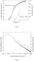
- Fig. 2 shows the curves of voltage-current density-luminance of the blue organic electroluminescent device obtained in Example 1. As seen from Fig. 2 , the lighting-up voltage of the device was 3.0 V, and the maximal luminance of the device was 10384 cd/m 2 .
- Fig. 3 shows the characteristic curves of current density-power efficiency-current efficiency of the blue organic electroluminescent device obtained in Example 1. As seen from Fig. 3 , the maximal current efficiency of the device is 6.41 cd/A, and the maximal power efficiency is 6.71 lm/W.
- Fig. 4 shows a spectrum of the blue organic electroluminescent device obtained in Example 1 when the luminance is 1000 cd/m 2 .
- the color coordinate of the device was (0.135, 0.138).
- An ITO anode layer on an ITO glass was laser-etched into a patterned electrode, then ultrasonically washed with a cleaning liquid and deionized water sequentially for 15 min, and placed in an oven for drying. The dried substrate was then placed in a pretreating vacuum chamber.
- the ITO anode was subjected to a low-pressure oxygen plasma treatment for 10 min under an atmosphere having a vacuum degree of 10 Pa with a voltage of 400 V, and then transferred to a metal vapor deposition chamber to vapor deposit 3 nm MoO 3 anode interface layer 3 under a vacuum atmosphere of 3 ⁇ 10 -5 to 5 ⁇ 10 -5 Pa.
- the uncompleted device was transferred to an organic vapor deposition chamber to sequentially vapor deposit a TAPC hole transport layer/electron blocking layer 4 with a thickness of 40 nm, a DBzA doped TcTa light emitting layer 5 with a thickness of 10 nm, and a Tm3PyP26PyB hole blocking layer/electron transport layer 6 with a thickness of 40 nm on the anode interface layer 3 under a vacuum atmosphere having a vacuum degree of 1 ⁇ 10 -5 to 3 ⁇ 10 -5 Pa.
- the uncompleted device was transferred to a metal vapor deposition chamber to vapor deposit a LiF buffer layer with a thickness of 1.0 nm under a vacuum atmosphere of 3 ⁇ 10 -5 to 5 ⁇ 10 -5 Pa.
- a metal Al electrode with a thickness of 120 nm was vapor deposited on the LiF layer through a specially-made mask plate to prepare a blue organic electroluminescent device having a structure of ITO/MoO 3 /TAPC/DBzA (15 wt%):TcTa/Tm3PyP26PyB/LiF/Al.
- the evaporation rates for DBzA and TcTa in the light emitting layer 5 were controlled at 0.0075 nm/s and 0.05 nm/s, respectively.
- the evaporation rates for TAPC and TmPyPB were controlled at 0.05 nm/s.
- the evaporation rate for MoO 3 was controlled at 0.01 nm/s.
- the evaporation rate for LiF was controlled at 0.005 nm/s.
- the evaporation rate for Al was controlled at 0.5 nm/s.
- the blue organic electroluminescent device obtained in Example 2 exhibited a pure blue light emission with a main peak at 462 nm under a direct voltage driving. As the operation voltage varied, the color coordinate of the device was stabilized in a range of from (0.133, 0.132) to (0.144, 0.143). When the luminance was 1000 cd/m 2 , the color coordinate of the device was (0.136, 0.134).
- Fig. 5 shows the curves of voltage-current density-luminance of the blue organic electroluminescent device obtained in Example 2. As seen from Fig. 5 , the luminance of the device increased as the current density and the driving voltage increased, the lighting-up voltage of the device was 2.8 V, and the maximal luminance of the device was 10937 cd/m 2 .
- Fig. 6 shows the characteristic curves of current density-power efficiency-current efficiency of the blue organic electroluminescent device obtained in Example 2. As seen from Fig. 6 , the maximal current efficiency of the device is 6.19 cd/A, and the maximal power efficiency is 6.51 Im/W.
- An ITO anode layer on an ITO glass was laser-etched into a patterned electrode, then ultrasonically washed with a cleaning liquid and deionized water sequentially for 15 min, and placed in an oven for drying. The dried substrate was then placed in a pretreating vacuum chamber.
- the ITO anode was subjected to a low-pressure oxygen plasma treatment for 10 min under an atmosphere having a vacuum degree of 10 Pa with a voltage of 400 V, and then transferred to a metal vapor deposition chamber to vapor deposit 3 nm MoO 3 anode interface layer 3 under a vacuum atmosphere of 3 ⁇ 10 -5 to 5 ⁇ 10 -5 Pa.
- the uncompleted device was transferred to an organic vapor deposition chamber to sequentially vapor deposit a TAPC hole transport layer/electron blocking layer 4 with a thickness of 50 nm, a DBzA doped TcTa light emitting layer 5 with a thickness of 10 nm, and a TmPyPB hole blocking layer/electron transport layer 6 with a thickness of 50 nm on the anode interface layer 3 under a vacuum atmosphere having a vacuum degree of 1 ⁇ 10 -5 to 3 ⁇ 10 -5 Pa.
- the uncompleted device was transferred to a metal vapor deposition chamber to vapor deposit a LiF buffer layer with a thickness of 1.0 nm under a vacuum atmosphere of 3 ⁇ 10 -5 to 5 ⁇ 10 -5 Pa.
- a metal Al electrode with a thickness of 120 nm was vapor deposited on the LiF layer through a specially-made mask plate to prepare a blue organic electroluminescent device having a structure of ITO/MoO 3 /TAPC/DBzA (16 wt%):TcTa/TmPyPB/LiF/Al.
- the evaporation rates for DBzA and TcTa in the light emitting layer 5 were controlled at 0.008 nm/s and 0.05 nm/s, respectively.
- the evaporation rates for TAPC and TmPyPB were controlled at 0.05 nm/s.
- the evaporation rate for MoO 3 was controlled at 0.01 nm/s.
- the evaporation rate for LiF was controlled at 0.005 nm/s.
- the evaporation rate for Al was controlled at 0.5 nm/s.
- the blue organic electroluminescent device obtained in Example 3 exhibited a pure blue light emission with a main peak at 462 nm under a direct voltage driving.
- the color coordinate of the device was stabilized in a range of from (0.135, 0.136) to (0.141, 0.149).
- the luminance was 1000 cd/m 2
- the color coordinate of the device was (0.137, 0.140).
- the lighting-up voltage of the device was 3.1 V
- the maximal luminance of the device was 11056 cd/m 2 .
- the maximal current efficiency of the device is 6.46 cd/A, and the maximal power efficiency is 6.54 lm/W.
- An ITO anode layer on an ITO glass was laser-etched into a patterned electrode, then ultrasonically washed with a cleaning liquid and deionized water sequentially for 15 min, and placed in an oven for drying. The dried substrate was then placed in a pretreating vacuum chamber.
- the ITO anode was subjected to a low-pressure oxygen plasma treatment for 10 min under an atmosphere having a vacuum degree of 10 Pa with a voltage of 400 V, and then transferred to a metal vapor deposition chamber to vapor deposit 3 nm MoO 3 anode interface layer 3 under a vacuum atmosphere of 3 ⁇ 10 -5 to 5 ⁇ 10 -5 Pa.
- the uncompleted device was transferred to an organic vapor deposition chamber to sequentially vapor deposit a TAPC hole transport layer/electron blocking layer 4 with a thickness of 50 nm, a DBzA doped TcTa light emitting layer 5 with a thickness of 10 nm, and a TmPyPB hole blocking layer/electron transport layer 6 with a thickness of 40 nm on the anode interface layer 3 under a vacuum atmosphere having a vacuum degree of 1 ⁇ 10 -5 to 3 ⁇ 10 -5 Pa.
- the uncompleted device was transferred to a metal vapor deposition chamber to vapor deposit a LiF buffer layer with a thickness of 1.0 nm under a vacuum atmosphere of 3 ⁇ 10 -5 to 5 ⁇ 10 -5 Pa.
- a metal Al electrode with a thickness of 120 nm was vapor deposited on the LiF layer through a specially-made mask plate to prepare an organic electroluminescent device having a structure of ITO/MoO 3 /TAPC/DBzA (16 wt%):TcTa/TmPyPB/LiF/Al.
- the evaporation rates for DBzA and TcTa in the light emitting layer 5 were controlled at 0.008 nm/s and 0.05 nm/s, respectively.
- the blue organic electroluminescent device obtained in Example 4 exhibited a pure blue light emission with a main peak at 462 nm under a direct voltage driving.
- the color coordinate of the device was stabilized in a range of from (0.131, 0.130) to (0.145, 0.141).
- the luminance was 1000 cd/m 2
- the color coordinate of the device was (0.132, 0.137).
- the lighting-up voltage of the device was 3.0 V
- the maximal luminance of the device was 11296 cd/m 2 .
- the maximal current efficiency of the device is 6.23 cd/A, and the maximal power efficiency is 6.52 Im/W.
- An ITO anode layer on an ITO glass was laser-etched into a patterned electrode, then ultrasonically washed with a cleaning liquid and deionized water sequentially for 15 min, and placed in an oven for drying. The dried substrate was then placed in a pretreating vacuum chamber.
- the ITO anode was subjected to a low-pressure oxygen plasma treatment for 10 min under an atmosphere having a vacuum degree of 10 Pa with a voltage of 400 V, and then transferred to a metal vapor deposition chamber to vapor deposit 3 nm MoO 3 anode interface layer 3 under a vacuum atmosphere of 3 ⁇ 10 -5 to 5 ⁇ 10 -5 Pa.
- the uncompleted device was transferred to an organic vapor deposition chamber to sequentially vapor deposit a TAPC hole transport layer/electron blocking layer 4 with a thickness of 40 nm, a DBzA doped TcTa light emitting layer 5 with a thickness of 10 nm, and a TmPyPB hole blocking layer/electron transport layer 6 with a thickness of 50 nm on the anode interface layer 3 under a vacuum atmosphere having a vacuum degree of 1 ⁇ 10 -5 to 3 ⁇ 10 -5 Pa.
- the uncompleted device was transferred to a metal vapor deposition chamber to vapor deposit a LiF buffer layer with a thickness of 1.0 nm under a vacuum atmosphere of 3 ⁇ 10 -5 to 5 ⁇ 10 -5 Pa.
- a metal Al electrode with a thickness of 120 nm was vapor deposited on the LiF layer through a specially-made mask plate to prepare a blue organic electroluminescent device having a structure of ITO/MoO 3 /TAPC/DBzA (16 wt%):TcTa/TmPyPB/LiF/Al.
- the evaporation rates for DBzA and TcTa in the light emitting layer 5 were controlled at 0.008 nm/s and 0.05 nm/s, respectively.
- the evaporation rates for TAPC and TmPyPB were controlled at 0.05 nm/s.
- the evaporation rate for MoO 3 was controlled at 0.01 nm/s.
- the evaporation rate for LiF was controlled at 0.005 nm/s.
- the evaporation rate for Al was controlled at 0.5 nm/s.
- the blue organic electroluminescent device obtained in Example 5 exhibited a pure blue light emission with a main peak at 462 nm under a direct voltage driving.
- the color coordinate of the device was stabilized in a range of from (0.135, 0.133) to (0.148, 0.146).
- the luminance was 1000 cd/m 2
- the color coordinate of the device was (0.139, 0.141).
- the lighting-up voltage of the device was 2.9 V
- the maximal luminance of the device was 9885 cd/m 2 .
- the maximal current efficiency of the device is 6.32 cd/A, and the maximal power efficiency is 6.84 lm/W.
- An ITO anode layer on an ITO glass was laser-etched into a patterned electrode, then ultrasonically washed with a cleaning liquid and deionized water sequentially for 15 min, and placed in an oven for drying. The dried substrate was then placed in a pretreating vacuum chamber.
- the ITO anode was subjected to a low-pressure oxygen plasma treatment for 10 min under an atmosphere having a vacuum degree of 10 Pa with a voltage of 400 V, and then transferred to a metal vapor deposition chamber to vapor deposit 3 nm MoO 3 anode interface layer 3 under a vacuum atmosphere of 3 ⁇ 10 -5 to 5 ⁇ 10 -5 Pa.
- the uncompleted device was transferred to an organic vapor deposition chamber to sequentially vapor deposit a TAPC hole transport layer/electron blocking layer 4 with a thickness of 50 nm, a DBzA doped TcTa light emitting layer 5 with a thickness of 10 nm, and a TmPyPB hole blocking layer/electron transport layer 6 with a thickness of 50 nm on the anode interface layer 3 under a vacuum atmosphere having a vacuum degree of 1 ⁇ 10 -5 to 3 ⁇ 10 -5 Pa.
- the uncompleted device was transferred to a metal vapor deposition chamber to vapor deposit a LiF buffer layer with a thickness of 1.0 nm under a vacuum atmosphere of 3 ⁇ 10 -5 to 5 ⁇ 10 -5 Pa.
- a metal Al electrode with a thickness of 120 nm was vapor deposited on the LiF layer through a specially-made mask plate to prepare an organic electroluminescent device having a structure of ITO/MoO 3 /TAPC/DBzA (15 wt%):TcTa/TmPyPB/LiF/Al.
- the evaporation rates for DBzA and TcTa in the light emitting layer 5 were controlled at 0.0075 nm/s and 0.05 nm/s, respectively.
- the evaporation rates for TAPC and TmPyPB were controlled at 0.05 nm/s.
- the evaporation rate for MoO 3 was controlled at 0.01 nm/s.
- the evaporation rate for LiF was controlled at 0.005 nm/s.
- the evaporation rate for Al was controlled at 0.5 nm/s.
- the blue organic electroluminescent device obtained in Example 6 exhibited a pure blue light emission with a main peak at 462 nm under a direct voltage driving.
- the color coordinate of the device was stabilized in a range of from (0.130, 0.135) to (0.142, 0.148).
- the luminance was 1000 cd/m 2
- the color coordinate of the device was (0.137, 0.143).
- the lighting-up voltage of the device was 3.0 V
- the maximal luminance of the device was 10656 cd/m 2 .
- the maximal current efficiency of the device is 6.28 cd/A, and the maximal power efficiency is 6.57 lm/W.
Landscapes
- Engineering & Computer Science (AREA)
- Physics & Mathematics (AREA)
- Chemical & Material Sciences (AREA)
- Materials Engineering (AREA)
- Spectroscopy & Molecular Physics (AREA)
- Optics & Photonics (AREA)
- Manufacturing & Machinery (AREA)
- Electroluminescent Light Sources (AREA)
Description
- The present invention relates to the technical field of organic electroluminescence, and particularly to a blue organic electroluminescent device and a preparation method thereof.
- An organic luminescent device is a device which spontaneously emits light. When charges are injected into an organic film between an electron injection electrode (an anode) and a hole injection electrode (a cathode), electrons and holes are combined and then annihilated to produce light. As compared to other flat display technologies such as liquid crystal display, plasma display device and field emission display, organic electroluminescent display has a series of excellent properties such as tunable luminescence color, active luminescence, high brightness, high efficiency, wide view angle, low energy consumption, simple preparation process, capability of preparing curved and flexible display screen, and so on, and has a wide application prospect in the field of large planar flat panel full color display, so it is considered as the most competitive new generation display technology. Therefore, research on organic electroluminescent technology has attracted more and more attentions and active participation of scientists and technicians in scientific community and industry community, such that the performances of organic electroluminescent device have been developed rapidly over the past decade. Among others, blue organic electroluminescent devices have become hot spots of investigation due to the wide prospect for application in terms of monochrome display, white light modulation, or the like.
- R&D (Research and Development) and design of high performance and high quality pure blue organic electroluminescent device have always been key and difficult point in the field. Transition metal complexes are regarded as ideal organic electroluminescent material by the academic community and industry community, due to their advantages such as high luminescence efficiency, tunable luminescence color, and so on. Many research groups, both domestic and abroad, set about material synthesis and device optimization, trying to improve the overall performances of blue organic electroluminescent devices in order to satisfy the requirements for industrialization. However, blue organic electroluminescent devices obtained based on transition metal complexes are usually accompanied by low color purity, low operating life, or low luminescence efficiency. Therefore, more and more research groups tend to replace blue transition metal complexes with blue fluorescence luminescent materials to obtain pure blue fluorescence organic electroluminescent devices. However, pure blue fluorescent materials generally have low luminescence efficiency. In addition, relatively wide energy gap of pure blue fluorescent materials results in great inconvenience for the screening of host materials, finally leading to unbalanced injection, transport and distribution of carriers. As a result, the blue luminescent devices prepared have relatively low luminescence efficiency and relatively high operation voltage.
- In order to solve these problems, domestic and abroad research groups devote themselves to design of new pure blue luminescent material and optimization of blue luminescent device structure. For example, Liang ZHOU et al. at Changchun Institute of Applied Chemistry, Chinese Academy of Sciences published a research article in Journal of Luminescence in 2010, which reported that a relatively stable pure blue luminescent device was obtained by incorporating trace amount of 8-hydroxylquinoline aluminum (AlQ), an electron transport material, into N,N'-di(1-naphthyl)-N,N'-diphenyl-1,1'-biphenyl-4,4'-diamine (NPB), a hole transport material emitting pure blue light. However, the device obtained had low luminescence efficiency, limiting its wide application in lighting and display fields. In 2014, Yuguang MA et al. at South China University of Technology reported in Laser Photonics Reviews that a new deep blue fluorescent material was developed and an excellent deep blue luminescent device was obtained. Although the deep blue device obtained had very excellent color purity and color stability, the high operation voltage thereof not only directly resulted in low power efficiency of the device, but also indirectly reduced the operation stability of the device. Other examples of blue luminescent materials and blue luminescent devices are shown in the following patent documents:
CN 102 024 909 A ,US 2011/291082 A1 andUS 2005/118456 A1 . - Thus, the overall performances of pure blue organic electroluminescent device comprising color purity, luminescence efficiency, operation stability and so on have not been substantially improved yet.
- In view of the above, the technical problem to be solved by the present invention is to provide a blue organic electroluminescent device and a preparation method thereof. The blue organic electroluminescent device has simple structure, and relatively high efficiency, luminance and operation stability.
- The present invention provides a blue organic electroluminescent device, comprising:
- a substrate;
- an anode layer disposed on the substrate;
- a light emitting layer disposed on the anode layer, the light emitting layer being formed from a blue organic fluorescent material and a hole-type organic host material, wherein the blue organic fluorescent material is 8.0% to 25.0% by mass of the hole-type organic host material, and an excited state energy of the blue organic fluorescent material is lower than an excited state energy of the hole-type organic host material; and
- a cathode layer disposed on the light emitting layer, wherein the blue organic fluorescent material is 2,2'-(9,10-anthracenediyl-di-4,1-phenylene)bis[6-methyl-benzothiazole] and wherein the hole-type organic host material is one or more selected from the group consisting of 4,4'-di(9-carbazolyl)biphenyl, 1,3-di(carbazol-9-yl)benzene, 9,9'-(5-(triphenylsilyl)-1,3-phenylene)-bis-9H-carbazole, 1,3,5-tri(9-carbazolyl)benzene, 4,4',4"-tri(carbazol-9-yl)triphenylamine and 4,4'-bis(triphenylsilyl)biphenyl.
- Preferably, the light emitting layer has a thickness of from 5 to 20 nm.
- Preferably, an anode interface layer is further disposed between the anode layer and the light emitting layer, wherein the anode interface layer has a thickness of from 2 to 10 nm.
- Preferably, a hole transport layer or electron blocking layer is further disposed between the anode layer and the light emitting layer, wherein the hole transport layer or electron blocking layer has a thickness of from 40 to 60 nm. In the presence of the anode interface layer, the hole transport layer or electron blocking layer is disposed between the anode interface layer and the light emitting layer.
- Preferably, a hole blocking layer or electron transport layer is further disposed between the light emitting layer and the cathode layer, wherein the hole blocking layer or electron transport layer has a thickness of from 40 to 60 nm.
- Preferably, a buffer layer is further disposed between the hole blocking layer or electron transport layer and the cathode layer, wherein the buffer layer has a thickness of from 0.8 to 1.2 nm.
- The present invention further provides a preparation method of a blue organic electroluminescent device, comprising:
- forming an anode layer on a substrate;
- forming a light emitting layer on the anode layer, the light emitting layer being formed from a blue organic fluorescent material and a hole-type organic host material, wherein the blue organic fluorescent material is 8.0% to 25.0% by mass of the hole-type organic host material, and an excited state energy of the blue organic fluorescent material is lower than an excited state energy of the hole-type organic host material; and
- forming a cathode on the light emitting layer, thereby obtaining the blue organic electroluminescent device, wherein the blue organic fluorescent material is 2,2'-(9,10-anthracenediyl-di-4,1-phenylene)bis[6-methyl-benzothiazole], and the hole-type organic host material is one or more selected from the group consisting of 4,4'-di(9-carbazolyl)biphenyl, 1,3-di(carbazol-9-yl)benzene, 9,9'-(5-(triphenylsilyl)-1,3-phenylene)bis-9H-carbazole, 1,3 ,5-tri (9-carbazolyl)benzene, 4,4',4"-tri(carbazol-9-yl)triphenylamine and 4,4'-bis(triphenylsilyl)biphenyl.
- The present invention provides a blue organic electroluminescent device comprising: a substrate; an anode layer disposed on the substrate; a light emitting layer disposed on the anode layer, the light emitting layer being formed from a blue organic fluorescent material and a hole-type organic host material, wherein the blue organic fluorescent material is 8.0% to 25.0% by mass of the hole-type organic host material, and an excited state energy of the blue organic fluorescent material is lower than an excited state energy of the hole-type organic host material; and a cathode layer disposed on the light emitting layer, wherein the blue organic fluorescent material is 2,2'-(9,10-anthracenediyl-di-4,1-phenylene)bis[6-methyl-benzothiazole], and the hole-type organic host material is one or more selected from the group consisting of 4,4'-di(9-carbazolyl)biphenyl, 1,3-di(carbazol-9-yl)benzene, 9,9'-(5-(triphenylsilyl)-1,3-phenylene)bis-9H-carbazole, 1,3 ,5-tri (9-carbazolyl)benzene, 4,4',4"-tri(carbazol-9-yl)triphenylamine and 4,4'-bis(triphenylsilyl)biphenyl. As compared to prior art, the 2,2'-(9,10-anthracenediyl-di-4,1-phenylene)bis[6-methyl-benzothiazole] blue organic fluorescent material with an excited state energy lower than that of the hole-type organic host material selected from the group consisting of 4,4'-di(9-carbazolyl)biphenyl, 1,3-di(carbazol-9-yl)benzene, 9,9'-(5-(triphenylsilyl)-1,3-phenylene)bis-9H-carbazole, 1,3 ,5-tri (9-carbazolyl)benzene, 4,4',4"-tri(carbazol-9-yl)triphenylamine and 4,4'-bis(triphenylsilyl)biphenyl, is used as luminescent material in the present invention, the 2,2'-(9,10-anthracenediyl-di-4,1-phenylene)bis[6-methyl-benzothiazole] blue organic fluorescent material having both high luminescence efficiency and high color purity as well as good thermostability, such that the color purity and efficiency of the device can be ensured. Meanwhile, the 2,2'-(9,10-anthracenediyl-di-4,1-phenylene)bis[6-methyl-benzothiazole] blue organic fluorescent material also has excellent electron transport capability, and as it is doped in the light emitting layer at a high concentration, the 2,2'-(9,10-anthracenediyl-di-4,1-phenylene)bis[6-methyl-benzothiazole] blue organic fluorescent material can function as both a host material and a blue luminescent material, which is beneficial for balancing the distribution of holes and electrons in the light emitting region, can confine the recombination of holes and electrons within the narrow region of the light emitting layer, and can effectively balance the distribution of carriers in the light emitting layer. In addition, the device provided in the present invention has simple structure and low cost, and all materials thereof have good thermostability, which is beneficial for improving the lifetime of the device.
-
-
Fig. 1 is a schematic structural diagram of a blue organic electroluminescent device provided in the present invention. -
Fig. 2 shows the characteristic curves of voltage-current density-luminance of the blue organic electroluminescent device obtained in Example 1 of the present invention. The luminance of the device increases as the current density and the driving voltage increase. The lighting-up voltage of the device is 3.0 volts (V). The maximal luminance of 10384 candelas per square meter (cd/m2) is obtained when the voltage is 8.4 V and the current density is 657.78 milliamperes per square centimeter (mA/cm2). -
Fig. 3 shows the characteristic curves of current density-power efficiency-current efficiency of the blue organic electroluminescent device obtained in Example 1 of the present invention. The maximal current efficiency of the device is 6.41 candelas per ampere (cd/A), and the maximal power efficiency is 6.71 lumens per watt (lm/W). -
Fig. 4 shows a spectrum of the blue organic electroluminescent device obtained in Example 1 of the present invention when the luminance is 1000 cd/m2. The color coordinate of the device is (0.135, 0.138). -
Fig. 5 shows the characteristic curves of voltage-current density-luminance of the blue organic electroluminescent device obtained in Example 2 of the present invention. The luminance of the device increases as the current density and the driving voltage increase. The lighting-up voltage of the device is 2.8 V. The maximal luminance of 10937 cd/m2 is obtained when the voltage is 8.0 V and the current density is 910.09 mA/cm2. -
Fig. 6 shows the characteristic curves of current density-power efficiency-current efficiency of the blue organic electroluminescent device obtained in Example 2 of the present invention. The maximal current efficiency of the device is 6.19 cd/A, and the maximal power efficiency is 6.51 Im/W. - The technical solutions in embodiments of the present invention will be detailedly described below in combination with the embodiments of the present invention. Obviously, the embodiments described are only a part of, not all of the embodiments of the present invention.
- The present invention provides a blue organic electroluminescent device, comprising:
- a substrate;
- an anode layer disposed on the substrate;
- a light emitting layer disposed on the anode layer, the light emitting layer being formed from a blue organic fluorescent material and a hole-type organic host material, wherein the blue organic fluorescent material is 8.0% to 25.0% by mass of the hole-type organic host material, and an excited state energy of the blue organic fluorescent material is lower than an excited state energy of the hole-type organic host material; and
- a cathode layer disposed on the light emitting layer, wherein the blue organic fluorescent material is 2,2'-(9,10-anthracenediyl-di-4,1-phenylene)bis[6-methyl-benzothiazole], and the hole-type organic host material is one or more selected from the group consisting of 4,4'-di(9-carbazolyl)biphenyl, 1,3-di(carbazol-9-yl)benzene, 9,9'-(5-(triphenylsilyl)-1,3-phenylene)bis-9H-carbazole, 1,3 ,5-tri (9-carbazolyl)benzene, 4,4',4"-tri(carbazol-9-yl)triphenylamine and 4,4'-bis(triphenylsilyl)biphenyl.
- There are no particular requirements on the substrate in the present invention, as long as it is a well-known substrate for those skilled in the art. The substrate is preferably a plastic substrate, a polymer substrate, a silicon-based substrate or a glass substrate, and more preferably a glass substrate.
- An anode layer is disposed on the substrate. The anode layer is formed from a material into which holes can be easily injected, preferably a conductive metal, a conductive metal oxide, or graphene, more preferably indium tin oxide, gold electrode, platinum electrode or graphene electrode, and still more preferably indium tin oxide. The indium tin oxide preferably has a surface resistance of 8 to 25 ohm.
- According to the present invention, an anode interface layer is preferably further disposed on the anode layer. The anode interface layer preferably has a thickness of 2 to 10 nm, more preferably 2 to 8 nm, still more preferably 2 to 5 nm, and the most preferably 3 nm. The anode interface layer is not specifically limited, as long as it is a well-known anode interface layer for those skilled in the art. In the present invention, the anode interface layer is preferably molybdenum trioxide, lithium fluoride or sodium chloride.
- In order to improve hole transport capability and meanwhile block electron transport so as to reduce the loss of the device and improve the efficiency of the device, a hole transport layer or electron blocking layer is preferably disposed on the anode interface layer. The hole transport layer or electron blocking layer preferably has a thickness of 40 to 60 nm, and more preferably 40 to 50 nm. The hole transport layer or electron blocking layer is not specifically limited, as long as it is a well-known hole transport layer or electron blocking layer for those skilled in the art. In the present invention, the hole transport layer or electron blocking layer is preferably formed from one or more selected from the group consisting of 4,4'-cyclohexylidene-bis[N,N-bis(4-methylphenyl)aniline] (TAPC), 4,4'-bis[N-(m-tolyl)-N-phenyl-amino]biphenyl (TPD) and N,N'-di(1-naphtyl)-N,N'-diphenyl-1,1'-biphenyl-4,4'-diamine (NPB), the molecular structural formulae of which are shown as follows:


- A light emitting layer is disposed on the hole transport layer or electron blocking layer. The light emitting layer is formed from a blue organic fluorescent material and a hole-type organic host material, wherein the blue organic fluorescent material is 2,2'-(9,10-anthracenediyl-di-4,1-phenylene)bis[6-methyl-benzothiazole], and the hole-type organic host material is one or more selected from the group consisting of 4,4'-di(9-carbazolyl)biphenyl, 1,3-di(carbazol-9-yl)benzene, 9,9'-(5-(triphenylsilyl)-1,3-phenylene)bis-9H-carbazole, 1,3 ,5-tri (9-carbazolyl)benzene, 4,4',4"-tri(carbazol-9-yl)triphenylamine and 4,4'-bis(triphenylsilyl)biphenyl.
- The light emitting layer preferably has a thickness of 5 to 20 nm, more preferably 5 to 15 nm, still more preferably 8 to 12 nm, and the most preferably 10 nm. The blue organic fluorescent material is 8.0% to 25.0%, preferably 10.0% to 25.0%, more preferably 15.0% to 20.0%, and even more preferably 15.0% to 16.0% by mass of the hole-type organic host material. The blue organic fluorescent material is a blue organic fluorescent material with matched energy and energy level. One basic principle for energy matching is that energy can be effectively transferred from the host material to the luminescent material, which requires that the excited state energy of the host material is greater than the excited state energy of the luminescent material. One basic principle for energy level matching is that the host material has a wide energy gap, which can effectively include the energy gap of the luminescent material so as to facilitate capture of carriers. In the present invention, the 2,2'-(9,10-anthracenediyl-di-4,1-phenylene)bis[6-methyl-benzothiazole] blue organic fluorescent material has an energy level favorable for electron injection into the light emitting region, and meanwhile function as an electron-type auxiliary host material. In the present invention, the blue organic fluorescent material is 2,2'-(9,10-anthracenediyl-di-4,1-phenylene)bis[6-methyl-benzothiazole] (DBzA, with a molecular formula as shown in formula I). The blue organic fluorescent material DBzA is the luminescent material, as it has both high luminescence efficiency and high color purity as well as good thermostability, and meanwhile has excellent electron transport capability, capable of effectively balancing the distribution of carriers in the light emitting layer. The hole-type organic host material is selected from the group of 4,4'-di(9-carbazolyl)biphenyl (CBP, with a molecular formula as shown in formula II), 1,3-di(carbazol-9-yl)benzene (mCP, with a molecular formula as shown in formula III), 9,9'-(5-(triphenylsilyl)-1,3-phenylene)bis-9H-carbazole (SimCP, with a molecular formula as shown in formula IV), 1,3,5-tri(9-carbazolyl)benzene (TCP, with a molecular formula as shown in formula V), 4,4',4"-tri(carbazol-9-yl)triphenylamine (TcTa, with a molecular formula as shown in formula VI) and 4,4'-bis(triphenylsilyl)biphenyl (BSB, with a molecular formula as shown in formula VII).


- In order to improve electron transport capability and meanwhile block hole transport so as to reduce the loss of the device and improve the efficiency of the device, a hole blocking layer or electron transport layer is preferably further disposed on the light emitting layer. The hole blocking layer or electron transport layer preferably has a thickness of 40 to 60 nm, more preferably 40 to 55 nm, and still more preferably 40 to 50 nm. The hole blocking layer or electron transport layer is not specifically limited, as long as it is a well-known hole blocking layer or electron transport layer for those skilled in the art. In the present invention, the hole blocking layer or electron transport layer is preferably formed from one or more selected from the group consisting of tris[2,4,6-trimethyl-3-(3-pyridyl)phenyl]borane (3TPYMB), 1,3,5-tri[(3-pyridyl)-3-phenyl]benzene (TmPyPB), 1,3-bis[3,5-di(3-pyridyl)phenyl]benzene (BmPyPhB), 1,3,5-tris(1-phenyl-1H-benzoimidazol-2-yl)benzene (TPBi) and 1,3,5-tris{6-[3-(pyridin-3-yl)phenyl]pyridin-2-yl}benzene (Tm3PyP26PyB), the molecular formulae of which are as shown in formulae VIII, IX, X, XI and XII.


- In order to increase the electron injection efficiency to further improve the efficiency of the device, a buffer layer is preferably further disposed on the hole blocking layer or electron transport layer. The buffer layer preferably has a thickness of 0.8 to 1.2 nm, more preferably 0.9 to 1.1 nm, and still more preferably 1 nm. The buffer layer is not specifically limited, as long as it is a well-known buffer layer for those skilled in the art. In the present invention, the buffer layer is preferably formed from lithium fluoride, sodium chloride or sodium carbonate.
- A cathode layer is disposed on the buffer layer. The cathode layer preferably has a thickness of 90 to 150 nm, more preferably 100 to 140 nm, still more preferably 110 to 130 nm, and the most preferably 120 nm. The cathode layer is not specifically limited, as long as it is a well-known cathode layer for those skilled in the art. In the present invention, the cathode layer is preferably formed from metal aluminum, magnesium silver alloy or silver.
- A schematic structural diagram of the blue organic electroluminescent device provided in the present invention is as shown in
Fig. 1 , wherein 1 represents a substrate, 2 represents an anode layer, 3 represents an anode interface layer, 4 represents a hole transport layer/electron blocking layer, 5 represents a light emitting layer, 6 represents a hole blocking layer/electron transport layer, 7 represents a buffer layer, and 8 represents a cathode layer. The anode and the cathode of the blue organic electroluminescent device are overlapped with each other to form a light emitting region. When a positive voltage is applied between these two electrodes, the device will emit a pure blue light with a main emission peak around 462 nm. - In the present invention, 2,2'-(9,10-anthracenediyl-di-4,1-phenylene)bis[6-methyl-benzothiazole] blue organic fluorescent material with an excited state energy lower than that of hole-type organic host material selected from the group consisting of 4,4'-di(9-carbazolyl)biphenyl, 1,3-di(carbazol-9-yl)benzene, 9,9'-(5-(triphenylsilyl)-1,3-phenylene)bis-9H-carbazole, 1,3 ,5-tri (9-carbazolyl)benzene, 4,4',4"-tri(carbazol-9-yl)triphenylamine and 4,4'-bis(triphenylsilyl)biphenyl, is used as a luminescent material, wherein the 2,2'-(9,10-anthracenediyl-di-4,1-phenylene)bis[6-methyl-benzothiazole] blue organic fluorescent material has both high luminescence efficiency and high color purity as well as good thermostability. As a result, the color purity and efficiency of the device can be ensured. Meanwhile, the 2,2'-(9,10-anthracenediyl-di-4,1-phenylene)bis[6-methyl-benzothiazole] blue organic fluorescent material also has excellent electron transport capability, and as it is doped in the light emitting layer at a high concentration, the 2,2'-(9,10-anthracenediyl-di-4,1-phenylene)bis[6-methyl-benzothiazole] blue organic fluorescent material can function as both a host material and a blue luminescent material, which is beneficial for balancing the distribution of holes and electrons in the light emitting region, can confine the recombination of holes and electrons within the narrow region of the light emitting layer, and can effectively balance the distribution of carriers in the light emitting layer. In addition, the device provided in the present invention has simple structure and low cost, and all materials thereof have good thermostability, which is beneficial for improving the lifetime of the device.
- The present invention also provides a preparation method of the above blue organic electroluminescent device, comprising the following steps:
- forming an anode layer on a substrate;
- forming a light emitting layer on the anode layer, the light emitting layer being formed from a blue organic fluorescent material and a hole-type organic host material, wherein the blue organic fluorescent material is 8.0% to 25.0% by mass of the hole-type organic host material, and an excited state energy of the blue organic fluorescent material is lower than an excited state energy of the hole-type organic host material; and
- forming a cathode on the light emitting layer, thereby obtaining a blue organic electroluminescent device, wherein the blue organic fluorescent material is 2,2'-(9,10-anthracenediyl-di-4,1-phenylene)bis[6-methyl-benzothiazole], and the hole-type organic host material is one or more selected from the group consisting of 4,4'-di(9-carbazolyl)biphenyl, 1,3-di(carbazol-9-yl)benzene, 9,9'-(5-(triphenylsilyl)-1,3-phenylene)bis-9H-carbazole, 1,3 ,5-tri (9-carbazolyl)benzene, 4,4',4"-tri(carbazol-9-yl)triphenylamine and 4,4'-bis(triphenylsilyl)biphenyl.
- According to the present invention, an anode layer is firstly formed on a substrate. The substrate and the anode layer are as described above, and will not be reiterated here. In the present invention, the electrode is preferably obtained by etching the conductive metal, conductive metal oxide, or graphene on the substrate. The shape and size of the electrode formed by etching are not specifically limited in the present invention. For example, a strip electrode with a width of 10 mm and a length of 30 mm may be formed by etching.
- Then, an anode interface layer is preferably formed on the anode layer. The anode interface layer is as described above and will not be reiterated here. In the present invention, preferably, the substrate with the anode layer formed thereon is washed and dried, and then the anode interface layer is formed on the anode layer. The process for forming the anode interface layer is not specifically limited, as long as it is a well-known process for those skilled in the art. In the present invention, preferably, the dried substrate with the anode layer formed is firstly subjected to a low pressure oxygen plasma treatment under vacuum condition, and then the anode interface layer is vapor deposited thereon. The vacuum degree for the vacuum condition is preferably 8 to 15 Pa. The voltage for the low pressure oxygen plasma treatment is 350 to 500 V. The time for the low pressure oxygen plasma treatment is preferably 5 to 15 min. The vacuum degree for the vapor deposition is preferably 5 × 10⁻⁵ to 8 × 10⁻⁵ Pa.
- Then, a hole transport layer or electron blocking layer is preferably formed on the anode interface layer. The hole transport layer or electron blocking layer is as described above and will not be reiterated here. The forming process is not specifically limited, as long as it is a well-known process for those skilled in the art. In the present invention, the process is preferably a vacuum vapor deposition process. The vacuum degree for the vapor deposition is preferably 1 × 10⁻⁵ to 3 × 10⁻⁵ Pa. The evaporation rate of organic material in the vacuum vapor deposition is preferably 0.05 to 0.1 nm/s.
- Then, a light emitting layer is formed on the hole transport layer or electron blocking layer. The light emitting layer is as described above and will not be reiterated here. The forming process is not specifically limited, as long as it is a well-known process for those skilled in the art. In the present invention, the process is preferably a vacuum vapor deposition process. The vacuum degree for the vapor deposition is preferably 1 × 10⁻⁵ to 3 × 10⁻⁵ Pa. The evaporation rate of blue organic fluorescent material in the vacuum vapor deposition is preferably 0.004 to 0.025 nm/s. The evaporation rate of hole-type organic host material in the vacuum vapor deposition is preferably 0.05 to 0.1 nm/s. The 2,2'-(9,10-anthracenediyl-di-4,1-phenylene)bis[6-methyl-benzothiazole] blue organic fluorescent material and the hole-type organic host material selected from the group consisting of 4,4'-di(9-carbazolyl)biphenyl, 1,3-di(carbazol-9-yl)benzene, 9,9'-(5-(triphenylsilyl)-1,3-phenylene)bis-9H-carbazole, 1,3 ,5-tri (9-carbazolyl)benzene, 4,4',4"-tri(carbazol-9-yl)triphenylamine and 4,4'-bis(triphenylsilyl)biphenyl, in the mixed organic material are evaporated simultaneously from different evaporation sources. The evaporation rates of these two materials are adjusted such that the blue organic fluorescent material is 8.0% to 25.0% by mass of the hole-type organic host material.
- According to the present invention, a hole blocking layer or electron transport layer is preferably formed on the light emitting layer. The hole blocking layer or electron transport layer is as described above and will not be reiterated here. The forming process is not specifically limited, as long as it is a well-known process for those skilled in the art. In the present invention, the process is preferably a vacuum vapor deposition process. The vacuum degree for the vapor deposition is preferably 1 × 10⁻⁵ to 3 × 10⁻⁵ Pa. The evaporation rate of organic material in the vacuum vapor deposition is preferably 0.05 to 0.1 nm/s.
- Then, a buffer layer is preferably formed on the hole blocking layer or electron transport layer. The buffer layer is as described above and will not be reiterated here. The forming process is not specifically limited, as long as it is a well-known process for those skilled in the art. In the present invention, the process is preferably a vacuum vapor deposition process. The vacuum degree for the vacuum vapor deposition is preferably 5 × 10⁻⁵ to 8 × 10⁻⁵ Pa. The evaporation rate is preferably 0.5 to 1.5 nm/s.
- Finally, a cathode layer is formed on the buffer layer, thereby obtaining a blue organic electroluminescent device. The cathode layer is as described above, and will not be reiterated here. The forming process is not specifically limited, as long as it is a well-known process for those skilled in the art. In the present invention, the process is preferably a vacuum vapor deposition process. The vacuum degree for the vacuum vapor deposition is preferably 5 × 10⁻⁵ to 8 × 10⁻⁵ Pa.
- The blue organic electroluminescent device provided in the present invention has a simple structure, which is favorable for simplifying the preparation process of the device. Meanwhile, according to
claim 1 generally have relatively low prices, which is favorable for lowering the manufacture cost of the device. In addition, all the materials used have good thermostability, which is favorable for improving the device lifetime. - By optimizing the device structure design and simplifying the device structure and the preparation process, the present invention improves the efficiency, luminance and operation stability of the device and reduces the manufacture cost of the device, on the premise that it is ensured that the color purity of the device is not reduced.
- In order to further illustrate the present invention, the blue organic electroluminescent device and the preparation method thereof provided in the present invention will be described in detail below with reference to examples.
- All reagents used in the following examples are commercially available.
- An ITO anode layer on an ITO glass was laser-etched into a patterned electrode, then ultrasonically washed with a cleaning liquid and deionized water sequentially for 15 min, and placed in an oven for drying. The dried substrate was then placed in a pretreating vacuum chamber. The ITO anode was subjected to a low-pressure oxygen plasma treatment for 10 min under an atmosphere having a vacuum degree of 10 Pa with a voltage of 400 V, and then transferred to a metal vapor deposition chamber to vapor deposit 3 nm MoO3 anode interface layer 3 under a vacuum atmosphere of 3 × 10⁻⁵ to 5 × 10⁻⁵ Pa. Then, the uncompleted device was transferred to an organic vapor deposition chamber to sequentially vapor deposit a TAPC hole transport layer/
electron blocking layer 4 with a thickness of 40 nm, a DBzA doped TcTalight emitting layer 5 with a thickness of 10 nm, and a TmPyPB hole blocking layer/electron transport layer 6 with a thickness of 40 nm on the anode interface layer 3 under a vacuum atmosphere having a vacuum degree of 1 × 10⁻⁵ to 3 × 10⁻⁵ Pa. Next, the uncompleted device was transferred to a metal vapor deposition chamber to vapor deposit a LiF buffer layer with a thickness of 1.0 nm under a vacuum atmosphere of 3 × 10⁻⁵ to 5 × 10⁻⁵ Pa. Finally, a metal Al electrode with a thickness of 120 nm was vapor deposited on the LiF layer through a specially-made mask plate to prepare a blue organic electroluminescent device having a structure of ITO/MoO3/TAPC/DBzA (16 wt%):TcTa/TmPyPB/LiF/Al. The evaporation rates for DBzA and TcTa in thelight emitting layer 5 were controlled at 0.008 nm/s and 0.05 nm/s, respectively. The evaporation rates for TAPC and TmPyPB were controlled at 0.05 nm/s. The evaporation rate for MoO3 was controlled at 0.01 nm/s. The evaporation rate for LiF was controlled at 0.005 nm/s. The evaporation rate for Al was controlled at 0.5 nm/s. - The blue organic electroluminescent device obtained in Example 1 exhibited a pure blue light emission with a main peak at 462 nm under a direct voltage driving. As the operation voltage varied, the color coordinate of the device was stabilized in a range of from (0.131, 0.133) to (0.146, 0.142). When the luminance was 1000 cd/m2, the color coordinate of the device was (0.135, 0.138).
-
Fig. 2 shows the curves of voltage-current density-luminance of the blue organic electroluminescent device obtained in Example 1. As seen fromFig. 2 , the lighting-up voltage of the device was 3.0 V, and the maximal luminance of the device was 10384 cd/m2. -
Fig. 3 shows the characteristic curves of current density-power efficiency-current efficiency of the blue organic electroluminescent device obtained in Example 1. As seen fromFig. 3 , the maximal current efficiency of the device is 6.41 cd/A, and the maximal power efficiency is 6.71 lm/W. -
Fig. 4 shows a spectrum of the blue organic electroluminescent device obtained in Example 1 when the luminance is 1000 cd/m2. The color coordinate of the device was (0.135, 0.138). - An ITO anode layer on an ITO glass was laser-etched into a patterned electrode, then ultrasonically washed with a cleaning liquid and deionized water sequentially for 15 min, and placed in an oven for drying. The dried substrate was then placed in a pretreating vacuum chamber. The ITO anode was subjected to a low-pressure oxygen plasma treatment for 10 min under an atmosphere having a vacuum degree of 10 Pa with a voltage of 400 V, and then transferred to a metal vapor deposition chamber to vapor deposit 3 nm MoO3 anode interface layer 3 under a vacuum atmosphere of 3 × 10⁻⁵ to 5 × 10⁻⁵ Pa. Then, the uncompleted device was transferred to an organic vapor deposition chamber to sequentially vapor deposit a TAPC hole transport layer/
electron blocking layer 4 with a thickness of 40 nm, a DBzA doped TcTalight emitting layer 5 with a thickness of 10 nm, and a Tm3PyP26PyB hole blocking layer/electron transport layer 6 with a thickness of 40 nm on the anode interface layer 3 under a vacuum atmosphere having a vacuum degree of 1 × 10⁻⁵ to 3 × 10⁻⁵ Pa. Next, the uncompleted device was transferred to a metal vapor deposition chamber to vapor deposit a LiF buffer layer with a thickness of 1.0 nm under a vacuum atmosphere of 3 × 10⁻⁵ to 5 × 10⁻⁵ Pa. Finally, a metal Al electrode with a thickness of 120 nm was vapor deposited on the LiF layer through a specially-made mask plate to prepare a blue organic electroluminescent device having a structure of ITO/MoO3/TAPC/DBzA (15 wt%):TcTa/Tm3PyP26PyB/LiF/Al. The evaporation rates for DBzA and TcTa in thelight emitting layer 5 were controlled at 0.0075 nm/s and 0.05 nm/s, respectively. The evaporation rates for TAPC and TmPyPB were controlled at 0.05 nm/s. The evaporation rate for MoO3 was controlled at 0.01 nm/s. The evaporation rate for LiF was controlled at 0.005 nm/s. The evaporation rate for Al was controlled at 0.5 nm/s. - The blue organic electroluminescent device obtained in Example 2 exhibited a pure blue light emission with a main peak at 462 nm under a direct voltage driving. As the operation voltage varied, the color coordinate of the device was stabilized in a range of from (0.133, 0.132) to (0.144, 0.143). When the luminance was 1000 cd/m2, the color coordinate of the device was (0.136, 0.134).
-
Fig. 5 shows the curves of voltage-current density-luminance of the blue organic electroluminescent device obtained in Example 2. As seen fromFig. 5 , the luminance of the device increased as the current density and the driving voltage increased, the lighting-up voltage of the device was 2.8 V, and the maximal luminance of the device was 10937 cd/m2. -
Fig. 6 shows the characteristic curves of current density-power efficiency-current efficiency of the blue organic electroluminescent device obtained in Example 2. As seen fromFig. 6 , the maximal current efficiency of the device is 6.19 cd/A, and the maximal power efficiency is 6.51 Im/W. - An ITO anode layer on an ITO glass was laser-etched into a patterned electrode, then ultrasonically washed with a cleaning liquid and deionized water sequentially for 15 min, and placed in an oven for drying. The dried substrate was then placed in a pretreating vacuum chamber. The ITO anode was subjected to a low-pressure oxygen plasma treatment for 10 min under an atmosphere having a vacuum degree of 10 Pa with a voltage of 400 V, and then transferred to a metal vapor deposition chamber to vapor deposit 3 nm MoO3 anode interface layer 3 under a vacuum atmosphere of 3 × 10⁻⁵ to 5 × 10⁻⁵ Pa. Then, the uncompleted device was transferred to an organic vapor deposition chamber to sequentially vapor deposit a TAPC hole transport layer/
electron blocking layer 4 with a thickness of 50 nm, a DBzA doped TcTalight emitting layer 5 with a thickness of 10 nm, and a TmPyPB hole blocking layer/electron transport layer 6 with a thickness of 50 nm on the anode interface layer 3 under a vacuum atmosphere having a vacuum degree of 1 × 10⁻⁵ to 3 × 10⁻⁵ Pa. Next, the uncompleted device was transferred to a metal vapor deposition chamber to vapor deposit a LiF buffer layer with a thickness of 1.0 nm under a vacuum atmosphere of 3 × 10⁻⁵ to 5 × 10⁻⁵ Pa. Finally, a metal Al electrode with a thickness of 120 nm was vapor deposited on the LiF layer through a specially-made mask plate to prepare a blue organic electroluminescent device having a structure of ITO/MoO3/TAPC/DBzA (16 wt%):TcTa/TmPyPB/LiF/Al. The evaporation rates for DBzA and TcTa in thelight emitting layer 5 were controlled at 0.008 nm/s and 0.05 nm/s, respectively. The evaporation rates for TAPC and TmPyPB were controlled at 0.05 nm/s. The evaporation rate for MoO3 was controlled at 0.01 nm/s. The evaporation rate for LiF was controlled at 0.005 nm/s. The evaporation rate for Al was controlled at 0.5 nm/s. - The blue organic electroluminescent device obtained in Example 3 exhibited a pure blue light emission with a main peak at 462 nm under a direct voltage driving. As the operation voltage varied, the color coordinate of the device was stabilized in a range of from (0.135, 0.136) to (0.141, 0.149). When the luminance was 1000 cd/m2, the color coordinate of the device was (0.137, 0.140). The lighting-up voltage of the device was 3.1 V, and the maximal luminance of the device was 11056 cd/m2. The maximal current efficiency of the device is 6.46 cd/A, and the maximal power efficiency is 6.54 lm/W.
- An ITO anode layer on an ITO glass was laser-etched into a patterned electrode, then ultrasonically washed with a cleaning liquid and deionized water sequentially for 15 min, and placed in an oven for drying. The dried substrate was then placed in a pretreating vacuum chamber. The ITO anode was subjected to a low-pressure oxygen plasma treatment for 10 min under an atmosphere having a vacuum degree of 10 Pa with a voltage of 400 V, and then transferred to a metal vapor deposition chamber to vapor deposit 3 nm MoO3 anode interface layer 3 under a vacuum atmosphere of 3 × 10⁻⁵ to 5 × 10⁻⁵ Pa. Then, the uncompleted device was transferred to an organic vapor deposition chamber to sequentially vapor deposit a TAPC hole transport layer/
electron blocking layer 4 with a thickness of 50 nm, a DBzA doped TcTalight emitting layer 5 with a thickness of 10 nm, and a TmPyPB hole blocking layer/electron transport layer 6 with a thickness of 40 nm on the anode interface layer 3 under a vacuum atmosphere having a vacuum degree of 1 × 10⁻⁵ to 3 × 10⁻⁵ Pa. Next, the uncompleted device was transferred to a metal vapor deposition chamber to vapor deposit a LiF buffer layer with a thickness of 1.0 nm under a vacuum atmosphere of 3 × 10⁻⁵ to 5 × 10⁻⁵ Pa. Finally, a metal Al electrode with a thickness of 120 nm was vapor deposited on the LiF layer through a specially-made mask plate to prepare an organic electroluminescent device having a structure of ITO/MoO3/TAPC/DBzA (16 wt%):TcTa/TmPyPB/LiF/Al. The evaporation rates for DBzA and TcTa in thelight emitting layer 5 were controlled at 0.008 nm/s and 0.05 nm/s, respectively. The evaporation rates for TAPC and TmPyPB were controlled at 0.05 nm/s. The evaporation rate for MoO3 was controlled at 0.01 nm/s. The evaporation rate for LiF was controlled at 0.005 nm/s. The evaporation rate for Al was controlled at 0.5 nm/s. - The blue organic electroluminescent device obtained in Example 4 exhibited a pure blue light emission with a main peak at 462 nm under a direct voltage driving. As the operation voltage varied, the color coordinate of the device was stabilized in a range of from (0.131, 0.130) to (0.145, 0.141). When the luminance was 1000 cd/m2, the color coordinate of the device was (0.132, 0.137). The lighting-up voltage of the device was 3.0 V, and the maximal luminance of the device was 11296 cd/m2. The maximal current efficiency of the device is 6.23 cd/A, and the maximal power efficiency is 6.52 Im/W.
- An ITO anode layer on an ITO glass was laser-etched into a patterned electrode, then ultrasonically washed with a cleaning liquid and deionized water sequentially for 15 min, and placed in an oven for drying. The dried substrate was then placed in a pretreating vacuum chamber. The ITO anode was subjected to a low-pressure oxygen plasma treatment for 10 min under an atmosphere having a vacuum degree of 10 Pa with a voltage of 400 V, and then transferred to a metal vapor deposition chamber to vapor deposit 3 nm MoO3 anode interface layer 3 under a vacuum atmosphere of 3 × 10⁻⁵ to 5 × 10⁻⁵ Pa. Then, the uncompleted device was transferred to an organic vapor deposition chamber to sequentially vapor deposit a TAPC hole transport layer/
electron blocking layer 4 with a thickness of 40 nm, a DBzA doped TcTalight emitting layer 5 with a thickness of 10 nm, and a TmPyPB hole blocking layer/electron transport layer 6 with a thickness of 50 nm on the anode interface layer 3 under a vacuum atmosphere having a vacuum degree of 1 × 10⁻⁵ to 3 × 10⁻⁵ Pa. Next, the uncompleted device was transferred to a metal vapor deposition chamber to vapor deposit a LiF buffer layer with a thickness of 1.0 nm under a vacuum atmosphere of 3 × 10⁻⁵ to 5 × 10⁻⁵ Pa. Finally, a metal Al electrode with a thickness of 120 nm was vapor deposited on the LiF layer through a specially-made mask plate to prepare a blue organic electroluminescent device having a structure of ITO/MoO3/TAPC/DBzA (16 wt%):TcTa/TmPyPB/LiF/Al. The evaporation rates for DBzA and TcTa in thelight emitting layer 5 were controlled at 0.008 nm/s and 0.05 nm/s, respectively. The evaporation rates for TAPC and TmPyPB were controlled at 0.05 nm/s. The evaporation rate for MoO3 was controlled at 0.01 nm/s. The evaporation rate for LiF was controlled at 0.005 nm/s. The evaporation rate for Al was controlled at 0.5 nm/s. - The blue organic electroluminescent device obtained in Example 5 exhibited a pure blue light emission with a main peak at 462 nm under a direct voltage driving. As the operation voltage varied, the color coordinate of the device was stabilized in a range of from (0.135, 0.133) to (0.148, 0.146). When the luminance was 1000 cd/m2, the color coordinate of the device was (0.139, 0.141). The lighting-up voltage of the device was 2.9 V, and the maximal luminance of the device was 9885 cd/m2. The maximal current efficiency of the device is 6.32 cd/A, and the maximal power efficiency is 6.84 lm/W.
- An ITO anode layer on an ITO glass was laser-etched into a patterned electrode, then ultrasonically washed with a cleaning liquid and deionized water sequentially for 15 min, and placed in an oven for drying. The dried substrate was then placed in a pretreating vacuum chamber. The ITO anode was subjected to a low-pressure oxygen plasma treatment for 10 min under an atmosphere having a vacuum degree of 10 Pa with a voltage of 400 V, and then transferred to a metal vapor deposition chamber to vapor deposit 3 nm MoO3 anode interface layer 3 under a vacuum atmosphere of 3 × 10⁻⁵ to 5 × 10⁻⁵ Pa. Then, the uncompleted device was transferred to an organic vapor deposition chamber to sequentially vapor deposit a TAPC hole transport layer/
electron blocking layer 4 with a thickness of 50 nm, a DBzA doped TcTalight emitting layer 5 with a thickness of 10 nm, and a TmPyPB hole blocking layer/electron transport layer 6 with a thickness of 50 nm on the anode interface layer 3 under a vacuum atmosphere having a vacuum degree of 1 × 10⁻⁵ to 3 × 10⁻⁵ Pa. Next, the uncompleted device was transferred to a metal vapor deposition chamber to vapor deposit a LiF buffer layer with a thickness of 1.0 nm under a vacuum atmosphere of 3 × 10⁻⁵ to 5 × 10⁻⁵ Pa. Finally, a metal Al electrode with a thickness of 120 nm was vapor deposited on the LiF layer through a specially-made mask plate to prepare an organic electroluminescent device having a structure of ITO/MoO3/TAPC/DBzA (15 wt%):TcTa/TmPyPB/LiF/Al. The evaporation rates for DBzA and TcTa in thelight emitting layer 5 were controlled at 0.0075 nm/s and 0.05 nm/s, respectively. The evaporation rates for TAPC and TmPyPB were controlled at 0.05 nm/s. The evaporation rate for MoO3 was controlled at 0.01 nm/s. The evaporation rate for LiF was controlled at 0.005 nm/s. The evaporation rate for Al was controlled at 0.5 nm/s. - The blue organic electroluminescent device obtained in Example 6 exhibited a pure blue light emission with a main peak at 462 nm under a direct voltage driving. As the operation voltage varied, the color coordinate of the device was stabilized in a range of from (0.130, 0.135) to (0.142, 0.148). When the luminance was 1000 cd/m2, the color coordinate of the device was (0.137, 0.143). The lighting-up voltage of the device was 3.0 V, and the maximal luminance of the device was 10656 cd/m2. The maximal current efficiency of the device is 6.28 cd/A, and the maximal power efficiency is 6.57 lm/W.
Claims (7)
- A blue organic electroluminescent device, comprising:a substrate (1);an anode layer (2) disposed on the substrate;a light emitting layer (5) disposed on the anode layer, the light emitting layer being formed from a blue organic fluorescent material and a hole-type organic host material, wherein an excited state energy of the blue organic fluorescent material is lower than an excited state energy of the hole-type organic host material; anda cathode layer (8) disposed on the light emitting layer,wherein the blue organic fluorescent material is 2,2'-(9,10-anthracenediyl-di-4,1-phenylene)bis[6-methyl-benzothiazole], and characterized in thatthe blue organic fluorescent material is 8.0% to 25.0% by mass of the hole-type organic host material, andthe hole-type organic host material is one or more selected from the group consisting of 4,4'-di(9-carbazolyl)biphenyl, 1,3-di(carbazol-9-yl)benzene, 9,9'-(5-(triphenylsilyl)-1,3-phenylene)bis-9H-carbazole, 1,3,5-tri(9-carbazolyl)benzene, 4,4',4"-tri(carbazol-9-yl)triphenylamine and 4,4'-bis(triphenylsilyl)biphenyl.
- The blue organic electroluminescent device according to claim 1, wherein the light emitting layer (5) has a thickness of from 5 to 20 nm.
- The blue organic electroluminescent device according to claim 1 or 2, wherein an anode interface layer (3) is further disposed between the anode layer (2) and the light emitting layer (5), wherein the anode interface layer has a thickness of from 2 to 10 nm.
- The blue organic electroluminescent device according to any one of claims 1 to 3, wherein a hole transport layer or electron blocking layer (4) is further disposed between the anode layer (2) and the light emitting layer (5), wherein the hole transport layer or electron blocking layer has a thickness of from 40 to 60 nm.
- The blue organic electroluminescent device according to any one of claims 1 to 4, wherein a hole blocking layer or electron transport layer (6) is further disposed between the light emitting layer (5) and the cathode layer (8), wherein the hole blocking layer or electron transport layer has a thickness of from 40 to 60 nm.
- The blue organic electroluminescent device according to claim 5, wherein a buffer layer (7) is further disposed between the hole blocking layer or electron transport layer (6) and the cathode layer (8), wherein the buffer layer has a thickness of from 0.8 to 1.2 nm.
- A preparation method of a blue organic electroluminescent device, comprising the steps of:forming an anode layer (2) on a substrate (1);forming a light emitting layer (5) on the anode layer (2), the light emitting layer being formed from a blue organic fluorescent material and a hole-type organic host material, wherein an excited state energy of the blue organic fluorescent material is lower than an excited state energy of the hole-type organic host material; andforming a cathode (8) on the light emitting layer (5), thereby obtaining the blue organic electroluminescent device,wherein the blue organic fluorescent material is 2,2'-(9,10-anthracenediyl-di-4,1-phenylene)bis[6-methyl-benzothiazole], and characterized in that the blue organic fluorescent material is 8.0% to 25.0% by mass of the hole-type organic host material, andthe hole-type organic host material is one or more selected from the group consisting of 4,4'-di(9-carbazolyl)biphenyl, 1,3-di(carbazol-9-yl)benzene, 9,9'-(5-(triphenylsilyl)-1,3-phenylene)bis-9H-carbazole, 1,3,5-tri(9-carbazolyl)benzene, 4,4',4"-tri(carbazol-9-yl)triphenylamine and 4,4'-bis(triphenylsilyl)biphenyl.
Applications Claiming Priority (2)
| Application Number | Priority Date | Filing Date | Title |
|---|---|---|---|
| CN201710032259.8A CN106803542B (en) | 2017-01-16 | 2017-01-16 | A blue organic electroluminescent device and preparation method thereof |
| PCT/CN2017/098005 WO2018129921A1 (en) | 2017-01-16 | 2017-08-18 | Blue organic electroluminescent device and preparation method therefor |
Publications (3)
| Publication Number | Publication Date |
|---|---|
| EP3570340A1 EP3570340A1 (en) | 2019-11-20 |
| EP3570340A4 EP3570340A4 (en) | 2020-10-14 |
| EP3570340B1 true EP3570340B1 (en) | 2025-02-26 |
Family
ID=58984501
Family Applications (1)
| Application Number | Title | Priority Date | Filing Date |
|---|---|---|---|
| EP17891195.4A Active EP3570340B1 (en) | 2017-01-16 | 2017-08-18 | Blue organic electroluminescent device and preparation method therefor |
Country Status (5)
| Country | Link |
|---|---|
| US (1) | US10854820B2 (en) |
| EP (1) | EP3570340B1 (en) |
| JP (1) | JP6825137B2 (en) |
| CN (1) | CN106803542B (en) |
| WO (1) | WO2018129921A1 (en) |
Families Citing this family (9)
| Publication number | Priority date | Publication date | Assignee | Title |
|---|---|---|---|---|
| CN106803542B (en) | 2017-01-16 | 2019-02-12 | 中国科学院长春应用化学研究所 | A blue organic electroluminescent device and preparation method thereof |
| CN106816542B (en) * | 2017-01-16 | 2018-10-16 | 中国科学院长春应用化学研究所 | A kind of white color organic electroluminescence device and preparation method thereof |
| CN109545990B (en) * | 2017-09-22 | 2021-05-28 | Tcl科技集团股份有限公司 | Electroluminescent device and preparation method and application thereof |
| CN108278533A (en) * | 2018-03-11 | 2018-07-13 | 哈尔滨医大眼科医疗科技开发有限公司 | A kind of hospital's irradiation light |
| CN108278534A (en) * | 2018-03-11 | 2018-07-13 | 哈尔滨医大眼科医疗科技开发有限公司 | A kind of hospital's special healthy lamp |
| JP2021125375A (en) * | 2020-02-05 | 2021-08-30 | 日本放送協会 | Quantum dot light-emitting element and display device |
| KR20220144032A (en) * | 2021-04-16 | 2022-10-26 | 삼성디스플레이 주식회사 | An light emitting device and electronic apparatus including the same |
| CN114267802B (en) * | 2021-12-14 | 2023-04-18 | 武汉华星光电半导体显示技术有限公司 | Light emitting device and display panel |
| CN116804015B (en) * | 2023-06-21 | 2023-12-29 | 季华恒烨(佛山)电子材料有限公司 | Blue light material, preparation method thereof and organic electroluminescent device |
Family Cites Families (17)
| Publication number | Priority date | Publication date | Assignee | Title |
|---|---|---|---|---|
| JP3561549B2 (en) * | 1995-04-07 | 2004-09-02 | 三洋電機株式会社 | Organic electroluminescence device |
| JP4057250B2 (en) * | 2001-04-09 | 2008-03-05 | 三星エスディアイ株式会社 | Organic EL element and organic EL display |
| JP3883999B2 (en) * | 2003-09-30 | 2007-02-21 | 三洋電機株式会社 | Organic electroluminescent device |
| JP3728309B2 (en) | 2003-09-30 | 2005-12-21 | 三洋電機株式会社 | Organic electroluminescent device and organic compound for organic electroluminescent device |
| KR101425378B1 (en) * | 2005-10-05 | 2014-08-01 | 가부시키가이샤 한도오따이 에네루기 켄큐쇼 | Stilbene derivatives, light-emitting element and light-emitting device |
| JP5194414B2 (en) * | 2006-09-21 | 2013-05-08 | 大日本印刷株式会社 | Organic electroluminescence device and method for manufacturing the same |
| CN101126020B (en) * | 2007-08-03 | 2012-11-28 | 深圳大学 | 1, 3, 6, 8-tetraaryl-9-alkyl substituted carbazole derivative and application thereof in luminescent diode |
| US8525159B2 (en) * | 2009-09-11 | 2013-09-03 | Sharp Kabushiki Kaisha | Organic light emitting element |
| WO2011162105A1 (en) * | 2010-06-25 | 2011-12-29 | Semiconductor Energy Laboratory Co., Ltd. | Light-emitting element, light-emitting device, display, and electronic device |
| CN102024909A (en) * | 2010-09-27 | 2011-04-20 | 电子科技大学 | Organic electroluminescence device with stable luminescence and preparation method thereof |
| CN102738414A (en) * | 2012-06-29 | 2012-10-17 | 中国科学院长春应用化学研究所 | Blue-ray fluorescent organic light emitting diode and manufacturing method thereof |
| JP6259812B2 (en) * | 2013-02-28 | 2018-01-10 | 株式会社カネカ | ORGANIC EL ELEMENT AND LIGHTING EQUIPMENT AND DISPLAY DEVICE USING THE SAME |
| WO2015167199A1 (en) * | 2014-04-29 | 2015-11-05 | Rohm And Haas Electronic Materials Korea Ltd. | Electron transport material and organic electroluminescent device comprising the same |
| JP6756613B2 (en) * | 2014-07-31 | 2020-09-16 | コニカミノルタ株式会社 | Organic electroluminescence device material, organic electroluminescence device, luminescent thin film, display device and lighting device |
| US10700294B2 (en) * | 2014-10-30 | 2020-06-30 | Changchun Institute Of Applied Chemistry, Chinese Academy Of Sciences | Blue organic electroluminescent device and preparation method thereof |
| JP2016195040A (en) * | 2015-03-31 | 2016-11-17 | セイコーエプソン株式会社 | LIGHT EMITTING DEVICE MANUFACTURING METHOD, LIGHT EMITTING DEVICE, AND ELECTRONIC DEVICE |
| CN106803542B (en) * | 2017-01-16 | 2019-02-12 | 中国科学院长春应用化学研究所 | A blue organic electroluminescent device and preparation method thereof |
-
2017
- 2017-01-16 CN CN201710032259.8A patent/CN106803542B/en active Active
- 2017-08-18 US US16/477,282 patent/US10854820B2/en active Active
- 2017-08-18 JP JP2019559136A patent/JP6825137B2/en active Active
- 2017-08-18 EP EP17891195.4A patent/EP3570340B1/en active Active
- 2017-08-18 WO PCT/CN2017/098005 patent/WO2018129921A1/en not_active Ceased
Non-Patent Citations (1)
| Title |
|---|
| YANAN LI ET AL: "High performance pure blue organic fluorescent electroluminescent devices by utilizing a traditional electron transport material as the emitter", JOURNAL OF MATERIALS CHEMISTRY C, vol. 5, no. 17, 1 January 2017 (2017-01-01), GB, pages 4219 - 4225, XP055727802, ISSN: 2050-7526, DOI: 10.1039/C7TC00725F * |
Also Published As
| Publication number | Publication date |
|---|---|
| WO2018129921A1 (en) | 2018-07-19 |
| EP3570340A1 (en) | 2019-11-20 |
| US20200035926A1 (en) | 2020-01-30 |
| CN106803542B (en) | 2019-02-12 |
| EP3570340A4 (en) | 2020-10-14 |
| JP6825137B2 (en) | 2021-02-03 |
| CN106803542A (en) | 2017-06-06 |
| JP2020510322A (en) | 2020-04-02 |
| US10854820B2 (en) | 2020-12-01 |
Similar Documents
| Publication | Publication Date | Title |
|---|---|---|
| US10854820B2 (en) | Blue organic electroluminescent device and preparation method thereof | |
| EP3570341B1 (en) | White organic electroluminescent device and preparation method therefor | |
| JP6385575B2 (en) | Red organic electroluminescence device and method for producing the same | |
| CN102983286B (en) | Green organic light emitting diode and preparation method thereof | |
| CN102751449B (en) | Organic light emitting diode | |
| JP6456497B2 (en) | Blue organic electroluminescence device and method for producing the same | |
| KR100469240B1 (en) | Organic electroluminescent device | |
| CN101384112A (en) | A kind of red organic electroluminescence device and preparation method thereof | |
| CN106450020A (en) | High-efficiency white light OLED device structure based on novel exciplex main body | |
| Liu et al. | Improved color quality in double-EML WOLEDs by using a tetradentate Pt (II) complex as a green/red emitter | |
| CN111682125A (en) | Organic light emitting diode display device, method of manufacturing the same, and display panel | |
| EP3557646B1 (en) | Organic electroluminescent device | |
| Fang et al. | Bisindoles containing a 2, 1, 3-benzothiadiazole unit: novel non-doping red organic light-emitting diodes with excellent color purity | |
| CN102983288A (en) | Blue-green organic electroluminescent device and manufacturing method thereof | |
| CN112909191B (en) | Light-emitting device structure and preparation method thereof, display substrate and display device | |
| CN111740020B (en) | High-efficiency long-service-life blue light device | |
| WO2015001691A1 (en) | Organic electroluminescent element | |
| WO2016065679A1 (en) | Yellow organic electroluminescent device and preparation method thereof | |
| WO2016065680A1 (en) | Green organic electroluminescent device and preparation method thereof | |
| CN106654034B (en) | A kind of Green organic light emitting diode and preparation method thereof | |
| CN110350095A (en) | Electroluminescent device and preparation method thereof, electronic equipment | |
| Gebeyehu | Highly efficient pin type organic light-emitting diodes using doping of the transport and emission layers | |
| US20220223815A1 (en) | Organic electroluminescent device | |
| CN106684255A (en) | Red organic light-emitting device and preparation method thereof |
Legal Events
| Date | Code | Title | Description |
|---|---|---|---|
| STAA | Information on the status of an ep patent application or granted ep patent |
Free format text: STATUS: THE INTERNATIONAL PUBLICATION HAS BEEN MADE |
|
| PUAI | Public reference made under article 153(3) epc to a published international application that has entered the european phase |
Free format text: ORIGINAL CODE: 0009012 |
|
| STAA | Information on the status of an ep patent application or granted ep patent |
Free format text: STATUS: REQUEST FOR EXAMINATION WAS MADE |
|
| 17P | Request for examination filed |
Effective date: 20190712 |
|
| AK | Designated contracting states |
Kind code of ref document: A1 Designated state(s): AL AT BE BG CH CY CZ DE DK EE ES FI FR GB GR HR HU IE IS IT LI LT LU LV MC MK MT NL NO PL PT RO RS SE SI SK SM TR |
|
| AX | Request for extension of the european patent |
Extension state: BA ME |
|
| DAV | Request for validation of the european patent (deleted) | ||
| DAX | Request for extension of the european patent (deleted) | ||
| A4 | Supplementary search report drawn up and despatched |
Effective date: 20200916 |
|
| RIC1 | Information provided on ipc code assigned before grant |
Ipc: H01L 51/54 20060101AFI20200910BHEP |
|
| STAA | Information on the status of an ep patent application or granted ep patent |
Free format text: STATUS: EXAMINATION IS IN PROGRESS |
|
| 17Q | First examination report despatched |
Effective date: 20220104 |
|
| REG | Reference to a national code |
Ref country code: DE Ref legal event code: R079 Free format text: PREVIOUS MAIN CLASS: H01L0051500000 Ipc: H10K0085600000 Ref country code: DE Ref legal event code: R079 Ref document number: 602017088072 Country of ref document: DE Free format text: PREVIOUS MAIN CLASS: H01L0051500000 Ipc: H10K0085600000 |
|
| GRAP | Despatch of communication of intention to grant a patent |
Free format text: ORIGINAL CODE: EPIDOSNIGR1 |
|
| STAA | Information on the status of an ep patent application or granted ep patent |
Free format text: STATUS: GRANT OF PATENT IS INTENDED |
|
| RIC1 | Information provided on ipc code assigned before grant |
Ipc: H10K 101/40 20230101ALN20241018BHEP Ipc: H10K 50/11 20230101ALN20241018BHEP Ipc: H10K 85/40 20230101ALI20241018BHEP Ipc: H10K 85/60 20230101AFI20241018BHEP |
|
| INTG | Intention to grant announced |
Effective date: 20241031 |
|
| GRAS | Grant fee paid |
Free format text: ORIGINAL CODE: EPIDOSNIGR3 |
|
| GRAA | (expected) grant |
Free format text: ORIGINAL CODE: 0009210 |
|
| STAA | Information on the status of an ep patent application or granted ep patent |
Free format text: STATUS: THE PATENT HAS BEEN GRANTED |
|
| P01 | Opt-out of the competence of the unified patent court (upc) registered |
Free format text: CASE NUMBER: APP_67212/2024 Effective date: 20241219 |
|
| AK | Designated contracting states |
Kind code of ref document: B1 Designated state(s): AL AT BE BG CH CY CZ DE DK EE ES FI FR GB GR HR HU IE IS IT LI LT LU LV MC MK MT NL NO PL PT RO RS SE SI SK SM TR |
|
| REG | Reference to a national code |
Ref country code: GB Ref legal event code: FG4D |
|
| REG | Reference to a national code |
Ref country code: CH Ref legal event code: EP |
|
| REG | Reference to a national code |
Ref country code: DE Ref legal event code: R096 Ref document number: 602017088072 Country of ref document: DE |
|
| REG | Reference to a national code |
Ref country code: IE Ref legal event code: FG4D |
|
| REG | Reference to a national code |
Ref country code: NL Ref legal event code: MP Effective date: 20250226 |
|
| PG25 | Lapsed in a contracting state [announced via postgrant information from national office to epo] |
Ref country code: RS Free format text: LAPSE BECAUSE OF FAILURE TO SUBMIT A TRANSLATION OF THE DESCRIPTION OR TO PAY THE FEE WITHIN THE PRESCRIBED TIME-LIMIT Effective date: 20250526 |
|
| PG25 | Lapsed in a contracting state [announced via postgrant information from national office to epo] |
Ref country code: FI Free format text: LAPSE BECAUSE OF FAILURE TO SUBMIT A TRANSLATION OF THE DESCRIPTION OR TO PAY THE FEE WITHIN THE PRESCRIBED TIME-LIMIT Effective date: 20250226 |
|
| PG25 | Lapsed in a contracting state [announced via postgrant information from national office to epo] |
Ref country code: PL Free format text: LAPSE BECAUSE OF FAILURE TO SUBMIT A TRANSLATION OF THE DESCRIPTION OR TO PAY THE FEE WITHIN THE PRESCRIBED TIME-LIMIT Effective date: 20250226 |
|
| PG25 | Lapsed in a contracting state [announced via postgrant information from national office to epo] |
Ref country code: ES Free format text: LAPSE BECAUSE OF FAILURE TO SUBMIT A TRANSLATION OF THE DESCRIPTION OR TO PAY THE FEE WITHIN THE PRESCRIBED TIME-LIMIT Effective date: 20250226 |
|
| REG | Reference to a national code |
Ref country code: LT Ref legal event code: MG9D |
|
| PG25 | Lapsed in a contracting state [announced via postgrant information from national office to epo] |
Ref country code: NO Free format text: LAPSE BECAUSE OF FAILURE TO SUBMIT A TRANSLATION OF THE DESCRIPTION OR TO PAY THE FEE WITHIN THE PRESCRIBED TIME-LIMIT Effective date: 20250526 Ref country code: IS Free format text: LAPSE BECAUSE OF FAILURE TO SUBMIT A TRANSLATION OF THE DESCRIPTION OR TO PAY THE FEE WITHIN THE PRESCRIBED TIME-LIMIT Effective date: 20250626 |
|
| PG25 | Lapsed in a contracting state [announced via postgrant information from national office to epo] |
Ref country code: NL Free format text: LAPSE BECAUSE OF FAILURE TO SUBMIT A TRANSLATION OF THE DESCRIPTION OR TO PAY THE FEE WITHIN THE PRESCRIBED TIME-LIMIT Effective date: 20250226 |
|
| PG25 | Lapsed in a contracting state [announced via postgrant information from national office to epo] |
Ref country code: HR Free format text: LAPSE BECAUSE OF FAILURE TO SUBMIT A TRANSLATION OF THE DESCRIPTION OR TO PAY THE FEE WITHIN THE PRESCRIBED TIME-LIMIT Effective date: 20250226 |
|
| PG25 | Lapsed in a contracting state [announced via postgrant information from national office to epo] |
Ref country code: LV Free format text: LAPSE BECAUSE OF FAILURE TO SUBMIT A TRANSLATION OF THE DESCRIPTION OR TO PAY THE FEE WITHIN THE PRESCRIBED TIME-LIMIT Effective date: 20250226 Ref country code: PT Free format text: LAPSE BECAUSE OF FAILURE TO SUBMIT A TRANSLATION OF THE DESCRIPTION OR TO PAY THE FEE WITHIN THE PRESCRIBED TIME-LIMIT Effective date: 20250626 |
|
| PG25 | Lapsed in a contracting state [announced via postgrant information from national office to epo] |
Ref country code: GR Free format text: LAPSE BECAUSE OF FAILURE TO SUBMIT A TRANSLATION OF THE DESCRIPTION OR TO PAY THE FEE WITHIN THE PRESCRIBED TIME-LIMIT Effective date: 20250527 Ref country code: BG Free format text: LAPSE BECAUSE OF FAILURE TO SUBMIT A TRANSLATION OF THE DESCRIPTION OR TO PAY THE FEE WITHIN THE PRESCRIBED TIME-LIMIT Effective date: 20250226 |
|
| REG | Reference to a national code |
Ref country code: AT Ref legal event code: MK05 Ref document number: 1771982 Country of ref document: AT Kind code of ref document: T Effective date: 20250226 |
|
| PG25 | Lapsed in a contracting state [announced via postgrant information from national office to epo] |
Ref country code: SE Free format text: LAPSE BECAUSE OF FAILURE TO SUBMIT A TRANSLATION OF THE DESCRIPTION OR TO PAY THE FEE WITHIN THE PRESCRIBED TIME-LIMIT Effective date: 20250226 |
|
| PG25 | Lapsed in a contracting state [announced via postgrant information from national office to epo] |
Ref country code: SM Free format text: LAPSE BECAUSE OF FAILURE TO SUBMIT A TRANSLATION OF THE DESCRIPTION OR TO PAY THE FEE WITHIN THE PRESCRIBED TIME-LIMIT Effective date: 20250226 |
|
| PG25 | Lapsed in a contracting state [announced via postgrant information from national office to epo] |
Ref country code: DK Free format text: LAPSE BECAUSE OF FAILURE TO SUBMIT A TRANSLATION OF THE DESCRIPTION OR TO PAY THE FEE WITHIN THE PRESCRIBED TIME-LIMIT Effective date: 20250226 |
|
| PGFP | Annual fee paid to national office [announced via postgrant information from national office to epo] |
Ref country code: DE Payment date: 20250819 Year of fee payment: 9 |
|
| PG25 | Lapsed in a contracting state [announced via postgrant information from national office to epo] |
Ref country code: IT Free format text: LAPSE BECAUSE OF FAILURE TO SUBMIT A TRANSLATION OF THE DESCRIPTION OR TO PAY THE FEE WITHIN THE PRESCRIBED TIME-LIMIT Effective date: 20250226 |
|
| PG25 | Lapsed in a contracting state [announced via postgrant information from national office to epo] |
Ref country code: AT Free format text: LAPSE BECAUSE OF FAILURE TO SUBMIT A TRANSLATION OF THE DESCRIPTION OR TO PAY THE FEE WITHIN THE PRESCRIBED TIME-LIMIT Effective date: 20250226 |
|
| PGFP | Annual fee paid to national office [announced via postgrant information from national office to epo] |
Ref country code: FR Payment date: 20250827 Year of fee payment: 9 |
|
| PG25 | Lapsed in a contracting state [announced via postgrant information from national office to epo] |
Ref country code: CZ Free format text: LAPSE BECAUSE OF FAILURE TO SUBMIT A TRANSLATION OF THE DESCRIPTION OR TO PAY THE FEE WITHIN THE PRESCRIBED TIME-LIMIT Effective date: 20250226 Ref country code: EE Free format text: LAPSE BECAUSE OF FAILURE TO SUBMIT A TRANSLATION OF THE DESCRIPTION OR TO PAY THE FEE WITHIN THE PRESCRIBED TIME-LIMIT Effective date: 20250226 |
|
| PG25 | Lapsed in a contracting state [announced via postgrant information from national office to epo] |
Ref country code: RO Free format text: LAPSE BECAUSE OF FAILURE TO SUBMIT A TRANSLATION OF THE DESCRIPTION OR TO PAY THE FEE WITHIN THE PRESCRIBED TIME-LIMIT Effective date: 20250226 |
|
| PG25 | Lapsed in a contracting state [announced via postgrant information from national office to epo] |
Ref country code: SK Free format text: LAPSE BECAUSE OF FAILURE TO SUBMIT A TRANSLATION OF THE DESCRIPTION OR TO PAY THE FEE WITHIN THE PRESCRIBED TIME-LIMIT Effective date: 20250226 |
|
| REG | Reference to a national code |
Ref country code: DE Ref legal event code: R097 Ref document number: 602017088072 Country of ref document: DE |
|
| PLBE | No opposition filed within time limit |
Free format text: ORIGINAL CODE: 0009261 |
|
| STAA | Information on the status of an ep patent application or granted ep patent |
Free format text: STATUS: NO OPPOSITION FILED WITHIN TIME LIMIT |
|
| REG | Reference to a national code |
Ref country code: CH Ref legal event code: L10 Free format text: ST27 STATUS EVENT CODE: U-0-0-L10-L00 (AS PROVIDED BY THE NATIONAL OFFICE) Effective date: 20260107 |
|
| 26N | No opposition filed |
Effective date: 20251127 |
|
| REG | Reference to a national code |
Ref country code: CH Ref legal event code: H13 Free format text: ST27 STATUS EVENT CODE: U-0-0-H10-H13 (AS PROVIDED BY THE NATIONAL OFFICE) Effective date: 20260324 |
|
| PG25 | Lapsed in a contracting state [announced via postgrant information from national office to epo] |
Ref country code: MC Free format text: LAPSE BECAUSE OF FAILURE TO SUBMIT A TRANSLATION OF THE DESCRIPTION OR TO PAY THE FEE WITHIN THE PRESCRIBED TIME-LIMIT Effective date: 20250226 |
|
| PG25 | Lapsed in a contracting state [announced via postgrant information from national office to epo] |
Ref country code: LU Free format text: LAPSE BECAUSE OF NON-PAYMENT OF DUE FEES Effective date: 20250818 |
|
| PG25 | Lapsed in a contracting state [announced via postgrant information from national office to epo] |
Ref country code: CH Free format text: LAPSE BECAUSE OF NON-PAYMENT OF DUE FEES Effective date: 20250831 |
|
| GBPC | Gb: european patent ceased through non-payment of renewal fee |
Effective date: 20250818 |