EP3570329A1 - Display device - Google Patents
Display device Download PDFInfo
- Publication number
- EP3570329A1 EP3570329A1 EP19174211.3A EP19174211A EP3570329A1 EP 3570329 A1 EP3570329 A1 EP 3570329A1 EP 19174211 A EP19174211 A EP 19174211A EP 3570329 A1 EP3570329 A1 EP 3570329A1
- Authority
- EP
- European Patent Office
- Prior art keywords
- partition wall
- main chain
- display device
- electrode
- equal
- Prior art date
- Legal status (The legal status is an assumption and is not a legal conclusion. Google has not performed a legal analysis and makes no representation as to the accuracy of the status listed.)
- Granted
Links
- 0 CC(N)=*(C)C=C(COC(C=CC1N)=CC1=C)C=C Chemical compound CC(N)=*(C)C=C(COC(C=CC1N)=CC1=C)C=C 0.000 description 4
Images




Classifications
-
- H—ELECTRICITY
- H10—SEMICONDUCTOR DEVICES; ELECTRIC SOLID-STATE DEVICES NOT OTHERWISE PROVIDED FOR
- H10K—ORGANIC ELECTRIC SOLID-STATE DEVICES
- H10K59/00—Integrated devices, or assemblies of multiple devices, comprising at least one organic light-emitting element covered by group H10K50/00
- H10K59/10—OLED displays
- H10K59/12—Active-matrix OLED [AMOLED] displays
- H10K59/122—Pixel-defining structures or layers, e.g. banks
-
- H—ELECTRICITY
- H10—SEMICONDUCTOR DEVICES; ELECTRIC SOLID-STATE DEVICES NOT OTHERWISE PROVIDED FOR
- H10K—ORGANIC ELECTRIC SOLID-STATE DEVICES
- H10K50/00—Organic light-emitting devices
- H10K50/10—OLEDs or polymer light-emitting diodes [PLED]
- H10K50/11—OLEDs or polymer light-emitting diodes [PLED] characterised by the electroluminescent [EL] layers
- H10K50/115—OLEDs or polymer light-emitting diodes [PLED] characterised by the electroluminescent [EL] layers comprising active inorganic nanostructures, e.g. luminescent quantum dots
-
- H—ELECTRICITY
- H10—SEMICONDUCTOR DEVICES; ELECTRIC SOLID-STATE DEVICES NOT OTHERWISE PROVIDED FOR
- H10K—ORGANIC ELECTRIC SOLID-STATE DEVICES
- H10K50/00—Organic light-emitting devices
- H10K50/80—Constructional details
-
- H—ELECTRICITY
- H10—SEMICONDUCTOR DEVICES; ELECTRIC SOLID-STATE DEVICES NOT OTHERWISE PROVIDED FOR
- H10K—ORGANIC ELECTRIC SOLID-STATE DEVICES
- H10K59/00—Integrated devices, or assemblies of multiple devices, comprising at least one organic light-emitting element covered by group H10K50/00
- H10K59/10—OLED displays
- H10K59/12—Active-matrix OLED [AMOLED] displays
-
- H—ELECTRICITY
- H10—SEMICONDUCTOR DEVICES; ELECTRIC SOLID-STATE DEVICES NOT OTHERWISE PROVIDED FOR
- H10K—ORGANIC ELECTRIC SOLID-STATE DEVICES
- H10K85/00—Organic materials used in the body or electrodes of devices covered by this subclass
- H10K85/10—Organic polymers or oligomers
- H10K85/111—Organic polymers or oligomers comprising aromatic, heteroaromatic, or aryl chains, e.g. polyaniline, polyphenylene or polyphenylene vinylene
-
- C—CHEMISTRY; METALLURGY
- C09—DYES; PAINTS; POLISHES; NATURAL RESINS; ADHESIVES; COMPOSITIONS NOT OTHERWISE PROVIDED FOR; APPLICATIONS OF MATERIALS NOT OTHERWISE PROVIDED FOR
- C09K—MATERIALS FOR MISCELLANEOUS APPLICATIONS, NOT PROVIDED FOR ELSEWHERE
- C09K11/00—Luminescent materials, e.g. electroluminescent or chemiluminescent
- C09K11/06—Luminescent materials, e.g. electroluminescent or chemiluminescent containing organic luminescent materials
-
- H—ELECTRICITY
- H10—SEMICONDUCTOR DEVICES; ELECTRIC SOLID-STATE DEVICES NOT OTHERWISE PROVIDED FOR
- H10K—ORGANIC ELECTRIC SOLID-STATE DEVICES
- H10K71/00—Manufacture or treatment specially adapted for the organic devices covered by this subclass
- H10K71/10—Deposition of organic active material
- H10K71/12—Deposition of organic active material using liquid deposition, e.g. spin coating
- H10K71/13—Deposition of organic active material using liquid deposition, e.g. spin coating using printing techniques, e.g. ink-jet printing or screen printing
- H10K71/135—Deposition of organic active material using liquid deposition, e.g. spin coating using printing techniques, e.g. ink-jet printing or screen printing using ink-jet printing
-
- H—ELECTRICITY
- H10—SEMICONDUCTOR DEVICES; ELECTRIC SOLID-STATE DEVICES NOT OTHERWISE PROVIDED FOR
- H10K—ORGANIC ELECTRIC SOLID-STATE DEVICES
- H10K85/00—Organic materials used in the body or electrodes of devices covered by this subclass
- H10K85/10—Organic polymers or oligomers
- H10K85/111—Organic polymers or oligomers comprising aromatic, heteroaromatic, or aryl chains, e.g. polyaniline, polyphenylene or polyphenylene vinylene
- H10K85/114—Poly-phenylenevinylene; Derivatives thereof
Definitions
- Embodiments relate to a display device.
- An inkjet printing device may be used to discharge fine droplets of an ink to a desired position on a printed medium and printing a predetermined image.
- An application range of the inkjet printing device may include, for example, various fields including a flat panel display field such as a liquid crystal display (LCD) and an organic light emitting device (OLED), a flexible display field such as an E-paper, a printed electronics field such as metal wires, and an organic thin film transistor (OTFT).
- a flat panel display field such as a liquid crystal display (LCD) and an organic light emitting device (OLED)
- OLED organic light emitting device
- E-paper organic light emitting device
- OTFT organic thin film transistor
- the present invention provides a display device, comprising a substrate, a thin film transistor provided on the substrate, a first electrode connected to the thin film transistor, a second electrode overlapping the first electrode, and a partition wall comprising a partition wall composition and a light-emitting device layer provided between the first electrode and the second electrode.
- the partition wall composition comprises a main chain and a side chain connected to the main chain, and a carbon number of the side chain is equal to or greater than 14.
- the main chain may be a polyimide-based polymer.
- the main chain may be a reaction product of a dianhydride compound and a diamine compound.
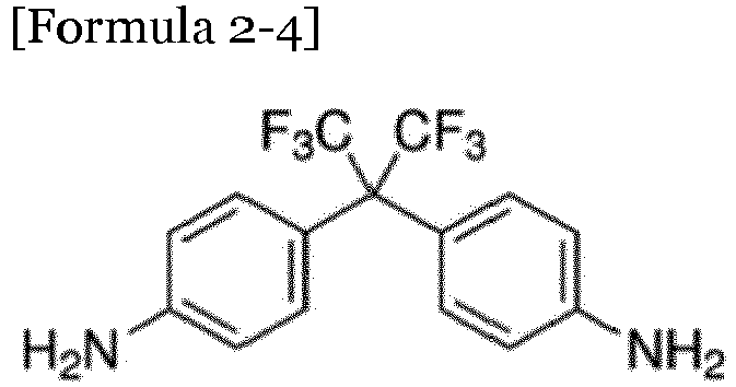
- the main chain may be a reaction product of at least one compound from among Formulae 1-1 to 1-6 and at least one compound from among Formulae 2-1 to 2-6:
- the side chain may comprise fluorine.
- the partition wall composition may comprise an addition product of an additive an the main chain, wherein the additive comprises fluorine, and at least one reactive group from among an acryl group, a methacryl group, an epoxy group, and a maleimide group that may react with the main chain.
- the addition product of the additive and the main chain may comprise a covalent bond formed between a portion derived from the additive and the main chain.
- the additive may be one or more of Formulae 3-1 to 3-6: wherein m1 and n1 may independently be an integer that is equal to or less than 30, n2 is an integer of 1 to 30, m3 and n3 may independently be an integer that is equal to or less than 30, and n4 may be an integer of 1 to 30.
- the side chain may be provided by a compound represented by Formula 4: wherein the X may be one of and l may be equal to or greater than 13.
- the partition wall composition may further include a reaction product of the main chain and one or more of an initiator, a crosslinking agent, a photoactive compound, or a surfactant.
- the present invention also provides a display device, comprising a substrate, a thin film transistor provided on the substrate, a first electrode connected to the thin film transistor, a second electrode overlapping the first electrode, and a partition wall comprising a partition wall composition and a light-emitting device layer provided between the first electrode and the second electrode.
- the partition wall composition comprises a main chain and a side chain connected to the main chain, the side chain comprising fluorine, and a carbon number of the side chain being be equal to or greater than 8.
- the side chain may comprise a number of fluorine atoms that is equal to or greater than 8.
- the side chain may be provided by one or more compound of Formulae 5-1 to 5-5: wherein,
- the main chain may be a polyimide-based polymer.
- the main chain may be a reaction product of a dianhydride compound and a diamine compound.
- the main chain may be a reaction product of at least one compound from among Formulae 1-1 to 1-6 and at least one compound from among Formulae 2-1 to 2-6:
- the partition wall composition may comprise an addition product of an additive and the main chain, wherein the additive comprises fluorine, and at least one reactive group from among an acryl group, a methacryl group, an epoxy group, or a maleimide group that may react with the main chain.
- the addition product of the additive and the main chain may comprise a covalent bond formed between a portion derived from the additive and the main chain.
- the additive may be one of Formulae 3-1 to 3-6: wherein:
- the partition wall composition may further comprise a reaction product of the main chain with one or more of an initiator, a crosslinking agent, a photoactive compound, or a surfactant.
- the light-emitting device layer may further comprise an emission layer, and the emission layer may comprise a quantum dot material.
- the partition wall composition when the partition wall composition is described as comprising a main chain and a side chain "connected to" the main chain, the side chain is typically an oligomer or polymer chain covalently bound to the main chain.
- the partition wall composition may for example comprise a graft polymer, with one or more side chains grafted to the main chain.
- a carbon number of a side chain typically refers to the number of carbon atoms in each of one or more side chains.
- the side chain when the side chain is describes as being "provided by a compound" (e.g. provided by a compound represented by Formula 4), the compound is typically a compound which reacts with the main chain to form the side chain.
- a compound will typically comprise a functional group which will react with the main chain, but will not be fully retained in the side chain of the partition wall composition.
- the compound may comprise a carboxylic acid group which may react with the main chain to form, for example, an ester or an amide linkage between the side chain and the main chain in the partition wall composition.
- FIG. 1 illustrates a display device according to an example embodiment.
- the emissive display device includes a substrate 110, a thin film transistor (TFT) provided on the substrate 110, a first electrode 191 connected to the thin film transistor (TFT), a second electrode 270 overlapping the first electrode 191, a partition wall 380 provided between the first electrode 191 and the second electrode 270, and a light-emitting device layer 370.
- TFT thin film transistor
- the partition wall 380 includes a main chain and a side chain connected to the main chain.
- a carbon number of the side chain i.e., a number of carbons of the side chain, may be equal to or greater than 14.
- the side chain with a carbon number that is equal to or greater than 14 may help the partition wall 380 to be hydrophobic.
- the contact angle of the partition wall 380 may be equal to or greater than 80 degrees.
- FIG. 2 illustrates a configuration of a partition wall 380 according to an example embodiment.
- the partition wall 380 comprises a composition having a main chain 10 and a side chain 20 connected to the main chain 10, and an additive 30 is connected in a side chain form to the main chain 10.
- the side chain 20 has a carbon number that is equal to or greater than 14, it is arranged in a direction extending from, e.g., perpendicular to, the main chain 10.
- the side chain 20 may enhance hydrophobic properties of the partition wall 380.
- the additive 30 may comprise fluorine.
- the hydrophobic property of the partition wall 380 may be further improved by the fluorine comprised in the additive 30.
- the partition wall 380 may not comprise the additive 30.
- the partition wall 380 may be provided with a hydrophobic property by the side chain 20 with a carbon number that is equal to or greater than 14.
- the main chain of the partition wall 380 may be, for example, a polyimide-based polymer.
- the main chain 10 may be a reaction product of a dianhydride compound and a diamine compound.
- the main chain 10 may be a reaction product of at least one compound from among Formulae 1-1 to 1-6 and at least one compound from among Formulae 2-1 to 2-6.
- the main chain 10 may be a reaction product of:
- the main chain 10 may have a structure of Formula A:
- the side chain 20 may be provided by a compound represented by Formula 4:
- X may be one of and the l may be equal to or greater than 13.
- the * shows a position where X is combined to Formula 4.
- the main chain 10 may have a structure of Formula C:
- a sum of A and B is greater than 0 and may be, for example, 1 to 10,000.
- the OR may be, for example, one of or in which the A may be a C1 to C30 alkyl or a C6 to C30 aromatic.
- the OR may be, for example, in which a sum of m and n may be equal to or greater than 8, x may be 0 to 3, and K may be one of
- the A and B of the OR may comprise various structures of diamine and dianhydride. Further, part of the above-noted structure may be replaced with an amine.
- the additive 30 may comprise fluorine.
- the additive 30 may comprise at least one reactive group of an acryl group, a methacryl group, an epoxy group, or a maleimide group that may react with the main chain 10.
- the additive 30 may be connected in a side chain form to the main chain 10 through the reactive group.
- the additive 30 may be, for example, one of Formulae 3-1 to 3-6.
- n1 and n1 may independently be an integer that is equal to or less than 30, n2 may be an integer of 1 to 30, m3 and n3 may independently be an integer that is equal to or less than 30, and n4 may be an integer of 1 to 30.
- the partition wall 380 may further comprise a reaction product of one or more of an initiator, a crosslinking agent, a photoactive compound, or a surfactant.
- an initiator e.g., a photoactive compound
- a crosslinking agent e.g., a crosslinking agent
- a photoactive compound e.g., a photoactive compound
- a surfactant e.g., a surfactant to e.g., a surfactant.
- the partition wall 380 comprises a main chain 10 and a side chain 20 with a carbon number that is equal to or greater than 14 connected to the main chain 10, the partition wall may have a hydrophobic property while the partition wall 380 does not comprise fluorine.
- the contact angle of the partition wall 380 may be equal to or greater than 80 degrees.
- the contact angle of water drops of the distilled water with respect to the partition wall 380 may be equal to or greater than 80 degrees. Therefore, when the light-emitting device layer 370 is formed by the inkjet process, a material of the hydrophilic light-emitting device layer 370 may be prevented from overflowing outside the partition wall 380. Therefore, the light-emitting device layer 370 may be efficiently formed by the inkjet process.
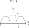
- FIG. 3 shows a spreading property of an inkjet material in a display device comprising a hydrophobic partition wall 380 according to an example embodiment
- FIG. 4 shows a spreading property of an inkjet material in a display device comprising a partition wall 380 according to a comparative example.
- the inkjet material 371 does not overflow the partition wall 380.
- the inkjet material 371 overflows the partition wall 380.
- a surface tension of the partition wall 380 may be equal to or less than 30 dyne/cm.
- the surface tension of the partition wall 380 may be equal to or greater than 40 dyne/cm.
- the comparative example may not have a sufficient hydrophobic property.
- the partition wall 380 when the partition wall 380 includes no fluorine, it may be hydrophobic because of the main chain 10 and the side chain 20 that is connected to the main chain 10 and it has a carbon number that is equal to or greater than 14.
- Tables 1 to 3 below show contact angles measured by changing carbon numbers of the side chain 20 and a number of CF 2 or CF 3 comprised in the side chain.
- a structure of a formula included as a main chain in Table 1, Table 2, and Table 3 is represented by Formula 7.
- Table 1 Contact angles (degrees) w/ H 2 O Numbers of CF 2 (CF 3 ) Carbon Number Nos. 0 Nos. 3 Nos. 4 Nos. 5 Nos. 7 Nos. 9 Nos. 11 Nos. 13 Nos.
- the main chain may comprise a compound represented by Formula 8 or Formula 9:
- X and Y may be 1 to 10,000, and a sum of m and n may be equal to or greater than 8. Further, the R' may be one of -H, alkyl, aromatic, OCO alkyl, or OCO halogen.
- a display device according to another example embodiment will now be described.
- a display device may correspond to the above-described example embodiments except that the side chain 20 of the partition wall 380 according to the present example embodiment comprises fluorine. Repeated description of details that are the same as the above-described constituent elements may be omitted for clarity.
- the side chain 20 comprises fluorine, and the carbon number of the side chain may be equal to or greater than 8.
- the side chain 20 comprises fluorine, and thus when the carbon number of the side chain is less than the above-described example embodiment, the partition wall may still exhibit a contact angle that is equal to or greater than 80 degrees.
- the side chain may comprise at least eight fluorine atoms.
- the side chain 20 may be formed by a reaction of one or more of Formulae 5-1 to 5-5:
- n1 and n1 may independently be an integer that is equal to or less than 30, n2 may be an integer of 5 to 30, m3 and n3 may independently be an integer that is equal to or less than 30, a sum of m3 and n3 may be equal to or greater than 2, n4 may be an integer of 6 to 30, X may be one of and n5 may be equal to or greater than 7.
- the main chain 10 may be a polyimide-based polymer.
- the main chain 10 may be a reaction product of a dianhydride compound and a diamine compound.
- the main chain 10 may be a reaction product of at least one compound from among Formulae 1-1 to 1-6 and at least one compound from among Formulae 2-1 to 2-6.
- the partition wall may have a structure represented by, for example, Formula B:
- the partition wall comprises a side chain connected to the main chain, and the side chain comprises fluorine.
- a partition wall formed using Formula B may have an enhanced hydrophobic property because of the side chain comprising fluorine.
- the partition wall may comprise an addition product of an additive 30.
- the additive 30 may comprise fluorine.
- the additive 30 may comprise at least one reactive group from among an acryl group, a methacryl group, an epoxy group, or a maleimide group that may react with the main chain 10.
- the additive 30 may be connected in a side chain form to the main chain 10 through the reactive group.
- the additive 30 may be, for example, one or more of Formulae 3-1 to 3-6:
- n1 and n1 may independently be an integer that is equal to or less than 30, n2 may be an integer of 1 to 30, m3 and n3 may independently be an integer that is equal to or less than 30, and n4 may be an integer of 1 to 30.
- the partition wall 380 may further comprise one or more of an initiator, a crosslinking agent, a photoactive compound, or a surfactant.
- the above-described example embodiment shows the hydrophobic property exhibiting the contact angle that is equal to or greater than 80 degrees when the fluorine number is 0 and the carbon number is equal to or greater than 14, and the partition wall composition according to the present example embodiment comprises fluorine, so it has the hydrophobic property that has the contact angle that is equal to or greater than 80 degrees when the carbon number is equal to or greater than 8.
- a side chain 20 or an additive 30 is connected to a main chain 10.
- a reaction for connecting the side chain 20 to the main chain 10 may be given as Reaction Formula 1:
- R'OH is a main chain
- RCOOH is a side chain or an additive
- RCOOH and R'OH When a thick sulfuric acid exists as a catalyst, RCOOH and R'OH generate an esterification reaction.
- a mole ratio of RCOOH and R'OH may be 2:1, for example.
- the reaction may be reversible and slow, and it may be performed slowly for about two hours or more at room temperature.
- a product that has undergone an esterification reaction is precipitated.
- the precipitated polymer is dried, a side chain connected to a main chain may be generated.
- it is possible to control a reaction rate of the side chain by controlling a content of the side chain material (RCOOH).
- RCOOH side chain material
- 3 mM of R'OH may be comprised, and 6 mM of RCOOH maybe comprised.
- the R'OH (the main chain) may be a compound represented by Formula A
- the RCOOH (the side chain) may be a compound represented by Formula C, for example.
- a display device comprising a partition wall according to an example embodiment will now be described in detail with reference to drawings.
- FIG. 5 shows a top plan view of a display device according to an example embodiment.
- FIG. 6 shows a cross-sectional view with respect to a line VI-VI' of FIG. 5 .
- the drawings show a 2Tr-1Cap-structured active-matrix (AM) emissive display device comprising two thin film transistors (TFTs) T1 and T2 and a capacitor C1 at each pixel of a display area, but this is merely an example.
- AM active-matrix
- one pixel may comprise at least three transistors and at least two capacitors, and additional wires may be further comprised to have various configurations.
- the pixel represents a minimum unit for displaying an image, and a display area displays an image through a plurality of pixels.
- the emissive display device comprises a switching thin film transistor T1, a driving thin film transistor T2, a capacitor C1, and a light-emitting device E1 respectively formed on a plurality of pixels provided on a substrate 110.
- the pixel may be defined by the gate line 121, the data line 171, and the common power line 172 as borders, for example.
- the light emitting element E1 comprises a first electrode 191, a light-emitting device layer 370 formed on the first electrode 191, and a second electrode 270 formed on the light-emitting device layer 370.
- the first electrode 191 is an anode that is a hole injection electrode
- the second electrode 270 is a cathode that is an electron injection electrode.
- the first electrode 191 may be a cathode and the second electrode 270 may be an anode depending on the method for driving an emissive display device.
- the first electrode 191 may be a pixel electrode
- the second electrode 270 may be a common electrode.
- the light-emitting device layer 370 may comprise one or more of a hole injection layer, a hole transfer layer, an emission layer, an electron transfer layer, or an electron injection layer.
- the emission layer may comprise an organic emission layer, and light emits when excitons that are generated when the injected holes and electrons are combined enter a ground state from an excited state.
- the emission layer may comprise a quantum dot.
- the emission layer may comprise blue, red, or green light emitting materials, and may further comprise a host and a dopant. The materials comprised in the emission layer are not limited.
- the emission layer may comprise blue emitting materials such as oxadiazole dimer dyes (e.g., bis-DAPOXP), spiro compounds (e.g., spiro-DPVBi, spiro-6P), triarylamine compounds, bis(styryl)amine compounds (e.g., DPVBi, DSA), 4,4'-bis(9-ethyl-3-carbazovinylene)-1,1'-biphenyl (BCzVBi), perylene, 2,5,8,11-tetra- tert -butyl perylene (TPBe), 9H-carbazol-3,3'-(1,4-phenylene-di-2,1-ethene-diyl)bis[9-ethyl-9C] (BCzVB), 4,4-bis[4-(di- p- tolylamino)styryl]biphenyl (DPAVBi), 4-(di- p -to-o
- a light emitting polymer material may be included.
- a polymer such as phenylene, poly(p-phenylene vinylene), thiophene, fluorene, spiro-fluorene, and/or the like, or an aromatic compound comprising nitrogen and/or the like may be included, but embodiments are not limited thereto.
- the emission layer may be manufactured by additionally doping a light emitting dopant into an emission layer host.
- Non-limiting examples of fluorescent light emitting host materials may include tris(8-hydroxy-quinolinato)aluminum (Alq3), 9,10-di(naphth-2-yl)anthracene (AND), 3- tert -butyl-9,10-di(naphth-2-yl)anthracene (TBADN), 4,4'-bis(2,2-diphenyl-ethene-1-yl)-4,4'-dimethylphenyl (DPVBi), 4,4'-bis(2,2-diphenyl-ethene-1-yl)-4,4'-methylphenyl (p-DMDPVBi), ter(9,9-diarylfluorene)s (TDAFs), 2-(9,9'-spirobifluorene-2-yl)-9,9'-spirobifluorene (BSDF), 2,7-bis(9,9'-spirobifluorene-2-yl)-9,9'
- the content of the light emitting dopant may vary according to the material forming the emission layer, but generally, the content of the light emitting dopant may be in a range of about 3 to about 10 parts by weight based on 100 parts by weight of the material forming the emission layer (total weight of the host and the dopant).
- a core of the quantum dot may be selected from among a group II-VI compound, a group III-V compound, a group IV-VI compound, a group IV element, a group IV compound, and a combination thereof.
- the group II-VI compound may be selected from among a binary compound selected from among CdSe, CdTe, ZnS, ZnSe, ZnTe, ZnO, HgS, HgSe, HgTe, MgSe, MgS, and a mixture thereof; a tertiary compound selected from among AgInS, CuInS, CdSeS, CdSeTe, CdSTe, ZnSeS, ZnSeTe, ZnSTe, HgSeS, HgSeTe, HgSTe, CdZnS, CdZnSe, CdZnTe, CdHgS, CdHgSe, CdHgTe, HgZnS, HgZnSe, HgZnTe, MgZnSe, MgZnS, and a mixture thereof; and a quaternary compound selected from among HgZnTeS, CdZnSeS,
- the group III-V compound may be selected from among a binary compound selected from among GaN, GaP, GaAs, GaSb, AlN, AlP, AlAs, AlSb, InN, InP, InAs, InSb, and a mixture thereof; a tertiary compound selected from among GaNP, GaNAs, GaNSb, GaPAs, GaPSb, AlNP, AlNAs, AlNSb, AlPAs, AlPSb, InGaP, InNP, InNAs, InNSb, InPAs, InPSb, GaAlNP, and a mixture thereof; and a quaternary compound selected from among GaAlNAs, GaAlNSb, GaAlPAs, GaAlPSb, GaInNP, GaInNAs, GaInNSb, GaInPAs, GaInPSb, InAlNP, InAlNAs, InAlNSb, InAlPAs, InAlPSb, and a mixture thereof.
- the group IV-VI compound may be selected from among a binary compound selected from among SnS, SnSe, SnTe, PbS, PbSe, PbTe, and a mixture thereof; a tertiary compound selected from among SnSeS, SnSeTe, SnSTe, PbSeS, PbSeTe, PbSTe, SnPbS, SnPbSe, SnPbTe, and a mixture thereof; and a quaternary compound selected from among SnPbSSe, SnPbSeTe, SnPbSTe, and a mixture thereof.
- the group IV element may be selected from among SI, Ge, and a mixture thereof.
- the group IV compound may be a binary compound selected from among SiC, SiGe, and a mixture thereof.
- the binary compound, the tertiary compound, or the quaternary compound may exist in particles at a uniform concentration, or may exist in the same particle divided into states where concentration distributions partially differ.
- the color conversion media layer may have a core/shell structure where one quantum dot surrounds another quantum dot.
- An interface between the core and the shell may have a concentration gradient such that a concentration of an element existing in the shell is gradually reduced nearing the center thereof.
- the quantum dot may have a core-shell configuration comprising a core comprising the nanocrystal and a shell surrounding the core.
- the shell of the quantum dot may function as a passivation layer for maintaining a semiconductor characteristic by preventing a chemical change of the core and/or function as a charging layer for assigning an electrophoretic characteristic to the quantum dot.
- the shell may be a single layer or a multilayer.
- An interface of the core and the shell may have a gradient of concentration in which the concentration of the element existing in the shell reduces as it approaches the center.
- An example of the shell of the quantum dot comprises an oxide of a metal or a non-metal, a semiconductor compound, or a combination thereof.
- the oxide of a metal or a non-metal may exemplify a binary compound such as SiO2, Al2O3, TiO2, ZnO, MnO, Mn2O3, Mn3O4, CuO, FeO, Fe2O3, Fe3O4, CoO, Co3O4, and NiO or a tertiary compound such as MgAl2O4, CoFe2O4, NiFe2O4, and CoMn2O4, and the present exemplary embodiment is not limited thereto.
- a binary compound such as SiO2, Al2O3, TiO2, ZnO, MnO, Mn2O3, Mn3O4, CuO, FeO, Fe2O3, Fe3O4, CoO, Co3O4, and NiO
- a tertiary compound such as MgAl2O4, CoFe2O4, NiFe2O4, and CoMn2O4, and the present exemplary embodiment is not limited thereto.
- the semiconductor compound may exemplify CdS, CdSe, CdTe, ZnS, ZnSe, ZnTe, ZnSeS, ZnTeS, GaAs, GaP, GaSb, HgS, HgSe, HgTe, InAs, InP, InGaP, InSb, AlAs, AlP, AlSb, and the present exemplary embodiment is not limited thereto.
- the quantum dot may have a full width at half maximum (FWHM) of an emission wavelength spectrum of about 45 nm or less, preferably about 40 nm or less, and more preferably about 30 nm or less, and in this range, color purity or color reproducibility may be improved.
- FWHM full width at half maximum
- the light emitted through the quantum dot is irradiated in all directions, thereby improving a light viewing angle.
- the form of the quantum dot is one generally used in the art and is not particularly limited, but more specifically, it may be formed to be spherical, pyramidal, multi-armed, or cubic nanoparticles, nanotubes, nanowires, nanofibers, and nanoplate-shaped particles.
- the quantum dot may control the colors of light emitted according to a size of particles, and the quantum dot may accordingly have various emitting colors such as red, green, and blue.
- the capacitor C1 comprises a pair of capacitive plates 158 and 178 disposed with an interlayer insulating layer 160 therebetween.
- the interlayer insulating layer 160 is a dielectric material. Capacitance is determined by charges stored in the capacitor C1 and a voltage between a pair of capacitive plates 158 and 178.
- the switching thin film transistor T1 comprises a switching semiconductor layer 151, a switching gate electrode 122, a switching source electrode 176, and a switching drain electrode 177.
- the driving thin film transistor T2 comprises a driving semiconductor layer 155, a driving gate electrode 124, a driving source electrode 173, and a driving drain electrode 175.
- the switching thin film transistor T1 is used as a switching element for selecting a pixel to emit.
- the switching gate electrode 122 is connected to the gate line 121, and the switching source electrode 176 is connected to the data line 171.
- the switching drain electrode 177 is separately disposed from the switching source electrode 176 and is connected to one capacitive plate 158.
- the driving thin film transistor T2 applies driving power for emitting the light-emitting device layer 370 of the light emitting element E1 in the selected pixel to the first electrode 191.
- the driving gate electrode 124 is connected to the capacitive plate 158 connected to the switching drain electrode 177.
- the driving source electrode 173 and the other capacitive plate 178 are respectively connected to the common power line 172.
- the driving drain electrode 175 is connected to the first electrode 191 through a contact hole 185.
- a buffer layer 111 is provided on the substrate 110.
- the substrate 110 may be made of glass, quartz, ceramic, or plastic.
- the buffer layer 111 may be made of a silicon nitride (SiN y ), a silicon oxide (SiO 2 ), a silicon oxynitride (SiO x N y ), etc.
- the x and y may respectively be 1 to 5, for example.
- a driving semiconductor layer 155 is formed on the buffer layer 111.
- the driving semiconductor layer 155 may be made of various semiconductor materials such as a polysilicon film or an amorphous silicon film.
- the driving semiconductor layer 155 may comprise a source region 152, a channel region 153, and a drain region 154.
- a gate insulating layer 140 made of a silicon nitride or a silicon oxide is provided on the driving semiconductor layer 155.
- a driving gate electrode 124 and a first capacitive plate 158 are provided on the gate insulating layer 140.
- the driving gate electrode 124 overlaps at least a portion of the driving semiconductor layer 155, in detail, the channel region 153.
- an interlayer insulating layer 160 covering the driving gate electrode 124 is provided on the gate insulating layer 140.
- the interlayer insulating layer 160 may be formed of a silicon nitride or a silicon oxide in a like manner of the gate insulating layer 140.
- the gate insulating layer 140 and the interlayer insulating layer 160 have a first contact hole 163 and a second contact hole 165 for exposing a source region 152 and a drain region 154 of the driving semiconductor layer 155.
- a driving source electrode 173, a driving drain electrode 175, a data line 171, a common power line 172, and a second capacitive plate 178 are provided on the interlayer insulating layer 160.
- the driving source electrode 173 and the driving drain electrode 175 are connected to the source region 152 and the drain region 154 of the driving semiconductor layer 155 through the first contact hole 163 and the second contact hole 165.
- an insulating layer 180 for covering the driving source electrode 173 and the driving drain electrode 175 is provided on the interlayer insulating layer 160.
- the insulating layer 180 may comprise an organic material such as a polyacryl or a polyimide.
- the insulating layer 180 comprises a contact hole 185.
- the first electrode 191 is provided on the insulating layer 180.
- the first electrode 191 may be a pixel electrode.
- the first electrode 191 is connected to the driving drain electrode 175 through the contact hole 185.
- the partition wall 380 is provided on the insulating layer 180.
- the description on the partition wall 380 corresponds to the above-provided descriptions of example embodiments.
- the partition wall 380 may comprise a main chain and a side chain connected to the main chain, the carbon number of the side chain may be 14, and the contact angle of the partition wall may be equal to or greater than 80 degrees.
- the partition wall 380 may comprise a main chain and a side chain connected to the main chain, the side chain may comprise fluorine, the carbon number of the side chain may be equal to or greater than 8, and the contact angle of the partition wall may be equal to or greater than 80 degrees. In this instance, the number of the fluorine atoms of the side chain may be equal to or greater than 8.
- the partition wall may further comprise an addition product of an additive comprising fluorine.
- the additive may comprise at least one reactive group from among the acryl group, the methacryl group, the epoxy group, or the maleimide group that may react with the main chain, and the additive may be connected in a side chain form to the main chain through the reactive group.
- the partition wall may further comprise one or more of the initiator, the crosslinking agent, the photoactive compound, or the surfactant.
- Detailed descriptions of the main chain, the side chain, and the additive of the partition wall 380 correspond to the above-provided descriptions.
- the light-emitting device layer 370 is provided to overlap the first electrode 191, and the second electrode 270 is provided to overlap the light-emitting device layer 370.
- the light-emitting device layer 370 may comprise one or more of the hole injection layer, the hole transfer layer, the emission layer, the electron transfer layer, or the electron injection layer.
- the second electrode 270 may be a common electrode.
- the light-emitting device E1 comprises a first electrode 191, a light-emitting device layer 370, and a second electrode 270.
- the partition wall 380 of the display device comprises a main chain 10 and a side chain 20 connected thereto.
- the side chain may not contain fluorine and the partition wall 380 may be hydrophobic without fluorine in the side chain, and the partition wall 380 may have the contact angle that is equal to or greater than 80 degrees.
- the partition wall 380 may have the contact angle that is equal to or greater than 80 degrees when the carbon number is equal to or greater than 8.
- the partition wall 380 with an excellent hydrophobic property by the side chain may prevent the inkjet material 371 from overflowing the partition wall 380 when the light-emitting device layer 370 is formed by the inkjet, and may efficiently form the light-emitting device layer 370.
- FIG. 7 shows a display device according to another exemplary embodiment of the present invention.
- the display device corresponds to the display device described with reference to FIG. 6 except for the configuration of a color converting panel 200. No description on the same configurational elements will be provided,
- the emission layer of the light-emitting device layer 370 may emit blue light.
- the blue light passes through the color converting layer 330 of the color converting panel 200 to be converted to red or green light or transmitted as blue through the converting layer.
- a color filter 230 is provided on a second substrate 210.
- the color filter 230 is provided between the first substrate 110 and the second substrate 210.
- a light blocking member 220 is provided between the color filter 230 and the second substrate 210, and the light blocking member 220 may partly overlap the color filter 230.
- a color filter insulating layer 250 is provided on the color filter 230 and the light blocking member 220.
- a color converting layer 330 is provided on the color filter insulating layer 250. That is, the color filter insulating layer 250 is provided between the color converting layer 330 and the color filter 230. The color converting layer 330 may be provided to overlap the color filter 230.
- the color converting layer 330 comprises a quantum dot and converts incident light into another color of light.
- a description on the quantum dot corresponds to the above-provided description.
- the color converting layer 330 may comprise a green color converting layer, a red color converting layer, and a blue color converting layer, and it may convert the blue light emitted by the light-emitting device layer 370 into green light or red light or transmit the blue light.
- An encapsulation layer 390 may be provided between the color converting panel 200 and the second electrode 270.
- the display panel comprising a light-emitting device layer 370 and the color converting panel 200 comprising a color converting layer 330 are combined.
- the light-emitting device layer 370 may emit blue light.
- the blue light passes through the color converting layer 330 and is converted into red light or green light by the respective color converting layers or is transmitted as blue light by the transmission layer.
- the light having transmitted through the color converting layer 330 passes through the respective color filters, and color purity is improved.
- the color filter 230 is prevented to not generate a color conversion on the color converting layer 330 by light input from the outside.
- a shape attached to a substrate in an earlier stage may be changed according to surface energy between the ink and the substrate to be printed.
- an emission layer if an emission layer is not correctly formed on a bank wall, an electrical short circuit may be generated, and/or a thickness of the emission layer may not be uniform so that brightness may not be uniform and a lifespan may be reduced. Further, when discharged droplets flow not inside but outside the bank, a short circuit may be generated or efficiency may be deteriorated.
- embodiments relate to a display device with a partition wall comprising a main chain and a side chain and having a hydrophobic property.
- Embodiments may provide a display device comprising a hydrophobic partition wall that comprises a main chain and a side chain connected thereto, and having a contact angle that is equal to or greater than 80 degrees.
- the present invention has been made in an effort to provide a display device for efficiently forming a light-emitting device layer by an inkjet process when a partition wall is hydrophobic.
- the display device has a hydrophobic partition wall, thereby efficiently forming the light-emitting device layer according to the inkjet process.
Landscapes
- Engineering & Computer Science (AREA)
- Chemical & Material Sciences (AREA)
- Physics & Mathematics (AREA)
- Optics & Photonics (AREA)
- Microelectronics & Electronic Packaging (AREA)
- Crystallography & Structural Chemistry (AREA)
- Inorganic Chemistry (AREA)
- Nanotechnology (AREA)
- Materials Engineering (AREA)
- Electroluminescent Light Sources (AREA)
Abstract
Description
- Korean Patent Application No.
10-2018-0054709, filed on May 14, 2018 10-2019-0041435, filed on April 9, 2019 - Embodiments relate to a display device.
- An inkjet printing device may be used to discharge fine droplets of an ink to a desired position on a printed medium and printing a predetermined image. An application range of the inkjet printing device may include, for example, various fields including a flat panel display field such as a liquid crystal display (LCD) and an organic light emitting device (OLED), a flexible display field such as an E-paper, a printed electronics field such as metal wires, and an organic thin film transistor (OTFT).
- The above information disclosed in this Background section is only for enhancement of understanding of the background of the invention and therefore it may contain information that does not form the prior art that is already known in this country to a person of ordinary skill in the art.
- The present invention provides a display device, comprising a substrate, a thin film transistor provided on the substrate, a first electrode connected to the thin film transistor, a second electrode overlapping the first electrode, and a partition wall comprising a partition wall composition and a light-emitting device layer provided between the first electrode and the second electrode. The partition wall composition comprises a main chain and a side chain connected to the main chain, and a carbon number of the side chain is equal to or greater than 14.
- The main chain may be a polyimide-based polymer.
- The main chain may be a reaction product of a dianhydride compound and a diamine compound.
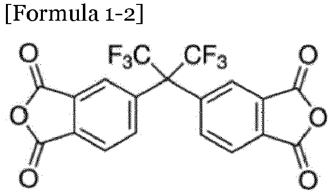
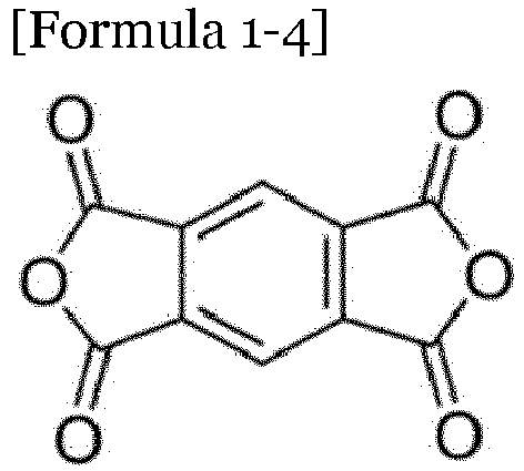
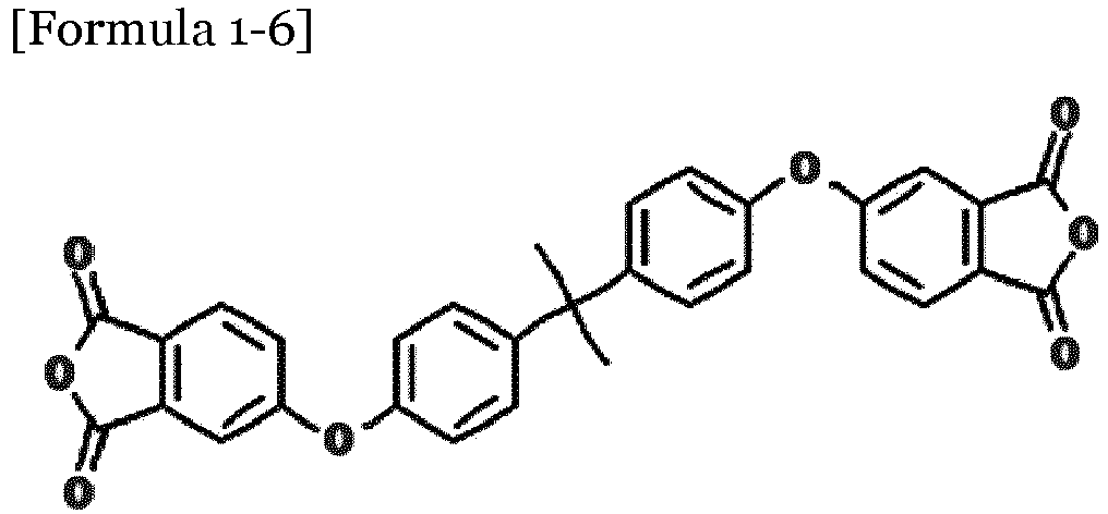
- The main chain may be a reaction product of at least one compound from among Formulae 1-1 to 1-6 and at least one compound from among Formulae 2-1 to 2-6:



- The side chain may comprise fluorine.
- The partition wall composition may comprise an addition product of an additive an the main chain, wherein the additive comprises fluorine, and at least one reactive group from among an acryl group, a methacryl group, an epoxy group, and a maleimide group that may react with the main chain.
- The addition product of the additive and the main chain may comprise a covalent bond formed between a portion derived from the additive and the main chain. The additive may be one or more of Formulae 3-1 to 3-6:


- The side chain may be provided by a compound represented by Formula 4:


l may be equal to or greater than 13. - The partition wall composition may further include a reaction product of the main chain and one or more of an initiator, a crosslinking agent, a photoactive compound, or a surfactant.
- The present invention also provides a display device, comprising a substrate, a thin film transistor provided on the substrate, a first electrode connected to the thin film transistor, a second electrode overlapping the first electrode, and a partition wall comprising a partition wall composition and a light-emitting device layer provided between the first electrode and the second electrode. The partition wall composition comprises a main chain and a side chain connected to the main chain, the side chain comprising fluorine, and a carbon number of the side chain being be equal to or greater than 8.
- The side chain may comprise a number of fluorine atoms that is equal to or greater than 8.
- The side chain may be provided by one or more compound of Formulae 5-1 to 5-5:


- m1 and n1 may independently be an integer that is equal to or less than 30,
- n2 may be an integer of 5 to 30,
- m3 and n3 may independently be an integer that is equal to or less than 30, provided that a sum of the m3 and n3 is equal to or greater than 2,
- n4 may be an integer of 6 to 30,
- n5 may be equal to or greater than 7, and
- X may be one of

- The main chain may be a polyimide-based polymer.
- The main chain may be a reaction product of a dianhydride compound and a diamine compound.
- The main chain may be a reaction product of at least one compound from among Formulae 1-1 to 1-6 and at least one compound from among Formulae 2-1 to 2-6:





- The partition wall composition may comprise an addition product of an additive and the main chain, wherein the additive comprises fluorine, and at least one reactive group from among an acryl group, a methacryl group, an epoxy group, or a maleimide group that may react with the main chain.
- The addition product of the additive and the main chain may comprise a covalent bond formed between a portion derived from the additive and the main chain.
- The additive may be one of Formulae 3-1 to 3-6:


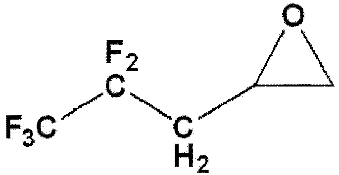

- m1 and n1 may independently be an integer that is equal to or less than 30,
- n2 may be an integer of 1 to 30,
- m3 and n3 may independently be an integer that is equal to or less than 30, and
- n4 may be an integer of 1 to 30.
- The partition wall composition may further comprise a reaction product of the main chain with one or more of an initiator, a crosslinking agent, a photoactive compound, or a surfactant.
- The light-emitting device layer may further comprise an emission layer, and the emission layer may comprise a quantum dot material.
- Features will become apparent to those of skill in the art by describing in detail example embodiments with reference to the attached drawings in which:
-
FIG. 1 illustrates a display device according to an example embodiment. -
FIG. 2 illustrates a configuration of a partition wall according to an example embodiment. -
FIG. 3 illustrates a spreading property of an inkjet material in a display device comprising a hydrophobic partition wall according to an example embodiment. -
FIG. 4 illustrates a spreading property of an inkjet material in a display device comprising a partition wall according to a comparative example of the present invention. -
FIG. 5 illustrates a top plan view of a display device according to an example embodiment. -
FIG. 6 illustrates a cross-sectional view with respect to a line VI-VI' ofFIG. 5 . -
FIG. 7 shows a same cross-section as that ofFIG. 6 in a display device according to another exemplary embodiment of the present invention. - Example embodiments will now be described more fully hereinafter with reference to the accompanying drawings; however, they may be embodied in different forms and should not be construed as limited to the embodiments set forth herein. Rather, these embodiments are provided so that this disclosure will be thorough and complete, and will fully convey example implementations to those skilled in the art. In the drawing figures, the dimensions of layers and regions may be exaggerated for clarity of illustration. Like reference numerals refer to like elements throughout.
- It will be understood that when an element such as a layer, film, region, or substrate is referred to as being "on" another element, it can be directly on the other element or intervening elements may also be present. In contrast, when an element is referred to as being "directly on" another element, there are no intervening elements present. The word "on" or "above" means positioned on or below the object portion, and does not necessarily mean positioned on the upper side of the object portion based on a gravitational direction.
- Unless explicitly described to the contrary, the word "comprise" and variations such as "comprises" or "comprising" will be understood to imply the inclusion of stated elements but not the exclusion of any other elements.
- The phrase "on a plane" means viewing the object portion from the top, and the phrase "on a cross-section" means viewing a cross-section of which the object portion is vertically cut from the side.
- As used herein, when the partition wall composition is described as comprising a main chain and a side chain "connected to" the main chain, the side chain is typically an oligomer or polymer chain covalently bound to the main chain. The partition wall composition may for example comprise a graft polymer, with one or more side chains grafted to the main chain.
- As used herein "a carbon number" of a side chain typically refers to the number of carbon atoms in each of one or more side chains.
- As used herein, when the side chain is describes as being "provided by a compound" (e.g. provided by a compound represented by Formula 4), the compound is typically a compound which reacts with the main chain to form the side chain. Such a compound will typically comprise a functional group which will react with the main chain, but will not be fully retained in the side chain of the partition wall composition. For example, the compound may comprise a carboxylic acid group which may react with the main chain to form, for example, an ester or an amide linkage between the side chain and the main chain in the partition wall composition.
-
FIG. 1 illustrates a display device according to an example embodiment. - Referring to
FIG. 1 , according to the present example embodiment, the emissive display device includes asubstrate 110, a thin film transistor (TFT) provided on thesubstrate 110, afirst electrode 191 connected to the thin film transistor (TFT), asecond electrode 270 overlapping thefirst electrode 191, apartition wall 380 provided between thefirst electrode 191 and thesecond electrode 270, and a light-emittingdevice layer 370. - According to the present example embodiment, the
partition wall 380 includes a main chain and a side chain connected to the main chain. A carbon number of the side chain, i.e., a number of carbons of the side chain, may be equal to or greater than 14. The side chain with a carbon number that is equal to or greater than 14 may help thepartition wall 380 to be hydrophobic. The contact angle of thepartition wall 380 may be equal to or greater than 80 degrees. -
FIG. 2 illustrates a configuration of apartition wall 380 according to an example embodiment. - Referring to
FIG. 2 , according to the present example embodiment, thepartition wall 380 comprises a composition having amain chain 10 and aside chain 20 connected to themain chain 10, and an additive 30 is connected in a side chain form to themain chain 10. - According to the present example embodiment, the
side chain 20 has a carbon number that is equal to or greater than 14, it is arranged in a direction extending from, e.g., perpendicular to, themain chain 10. Theside chain 20 may enhance hydrophobic properties of thepartition wall 380. - In an example embodiment, the additive 30 may comprise fluorine. The hydrophobic property of the
partition wall 380 may be further improved by the fluorine comprised in the additive 30. In another implementation, thepartition wall 380 may not comprise the additive 30. In this case, thepartition wall 380 may be provided with a hydrophobic property by theside chain 20 with a carbon number that is equal to or greater than 14. - The main chain of the
partition wall 380 may be, for example, a polyimide-based polymer. For example, themain chain 10 may be a reaction product of a dianhydride compound and a diamine compound. - For example, the
main chain 10 may be a reaction product of at least one compound from among Formulae 1-1 to 1-6 and at least one compound from among Formulae 2-1 to 2-6.
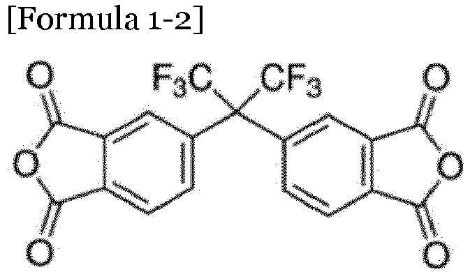


- In an example embodiment, the
main chain 10 may be a reaction product of: - a first compound that is one of pyromellitic acid dianhydride, 3,3',4,4'-biphenyl tetracarboxylic acid dianhydride, 2,3,3',4'-biphenyl tetracarboxylic acid dianhydride, 3,3',4,4'-benzophenone tetracarboxylic acid dianhydride, 3,3',4,4'-diphenyl ether tetracarboxylic acid dianhydride, 3,3'4,4'-diphenyl methane tetracarboxylic acid dianhydride, 2,2-bis(3,4-dicarboxylic phenyl)propane dianhydride, 2,2-bis(3,4-dicarboxylic phenyl)hexafluoropropane dianhydride, 3,3',4,4'-diphenyl sulfone tetracarboxylic acid dianhydride, 2,2-bis[4-(3,4-dicarboxylic phenoxy)phenyl]propane dianhydride, 4,4'-bis(3,4-dicarboxylic phenoxy)diphenyl ether dianhydride, 4,4'-bis(3,4-dicarboxylic phenoxy)diphenyl sulfide dianhydride, 4,4'-bis(3,4-dicarboxylic phenoxy)benzophenone dianhydride, 4,4'-bis(3,4-dicarboxylic phenoxy)diphenyl sulfone dianhydride, 2,2-bis[4-(2,3-dicarboxylic phenoxy)phenyl]propane dianhydride, 4,4'-bis(2,3-dicarboxylic phenoxy)diphenyl ether dianhydride, 4,4'-bis(2,3-dicarboxylic phenoxy)diphenyl sulfide dianhydride, 4,4'-bis(2,3-dicarboxylic phenoxy)benzophenone dianhydride, 4,4'-bis(2,3-dicarboxylic phenoxy)diphenyl sulfone dianhydride, 4-(2,3-dicarboxylic phenoxy)-4'-(3,4-dicarboxylic phenoxy)diphenyl-2,2-propane dianhydride, 4-(2,3-dicarboxylic phenoxy)-4'-(3,4-dicarboxylic phenoxy)diphenyl ether dianhydride, 4-(2,3-dicarboxylic phenoxy)-4'-(3,4-dicarboxylic phenoxy)diphenyl sulfide dianhydride, 4-(2,3-dicarboxylic phenoxy)-4'-(3,4-dicarboxylic phenoxy)benzophenone dianhydride, or 4-(2,3-dicarboxylic phenoxy)-4'-(3,4-dicarboxylic phenoxy)diphenyl sulfone dianhydride, and
- a second compound that is one of cyclic-based diamines including ethylene diamine, propylene diamine, trimethylene diamine, hexamethylene diamine, heptamethylene diamine, octamethylene diamine, nonamethylene diamine, decamethylene diamine, 1,12-dodecane diamine, 1,18-octadecane diamine, 3-methylheptamethylene diamine, 4,4-dimethylheptamethylene diamine, 4-methylnonamethylene diamine, 5-methylnona methylene diamine, 2,5-dimethylhexamethylene diamine, 2,5-dimethylheptamethylene diamine, 2,2-dimethylpropylene diamine, N-methyl-bis(3-aminopropyl)amine, 3-methoxyhexamethylene diamine, 1,2-bis(3-aminopropoxy)ethane, bis(3-aminopropyl)sulfide, 1,4-cyclohexane diamine, bis-(4-aminocyclohexyl)methane, or 1,3-diamino adamantane.
- In an example embodiment, the
main chain 10 may have a structure of Formula A:
- In an example embodiment, the
side chain 20 may be provided by a compound represented by Formula 4:
- In Formula 4, X may be one of

- In an example embodiment, the
main chain 10 may have a structure of Formula C:
- In Formula C, a sum of A and B is greater than 0 and may be, for example, 1 to 10,000.
- The OR may be, for example, one of


- In another implementation, the OR may be, for example,


- In addition to the above-noted structure, the A and B of the OR may comprise various structures of diamine and dianhydride. Further, part of the above-noted structure may be replaced with an amine.
- The additive 30 may comprise fluorine.
- The additive 30 may comprise at least one reactive group of an acryl group, a methacryl group, an epoxy group, or a maleimide group that may react with the
main chain 10. The additive 30 may be connected in a side chain form to themain chain 10 through the reactive group. - The additive 30 may be, for example, one of Formulae 3-1 to 3-6.


- In Formulae 3-1 to 3-6, m1 and n1 may independently be an integer that is equal to or less than 30, n2 may be an integer of 1 to 30, m3 and n3 may independently be an integer that is equal to or less than 30, and n4 may be an integer of 1 to 30.
- The
partition wall 380 may further comprise a reaction product of one or more of an initiator, a crosslinking agent, a photoactive compound, or a surfactant. When thepartition wall 380 is a positive photoresist, it may comprise a photoactive compound, and when thepartition wall 380 is a negative photoresist, it may comprise an initiator. - When the
partition wall 380 comprises amain chain 10 and aside chain 20 with a carbon number that is equal to or greater than 14 connected to themain chain 10, the partition wall may have a hydrophobic property while thepartition wall 380 does not comprise fluorine. In this instance, the contact angle of thepartition wall 380 may be equal to or greater than 80 degrees. Thus, when distilled water is dripped on thepartition wall 380, the contact angle of water drops of the distilled water with respect to thepartition wall 380 may be equal to or greater than 80 degrees. Therefore, when the light-emittingdevice layer 370 is formed by the inkjet process, a material of the hydrophilic light-emittingdevice layer 370 may be prevented from overflowing outside thepartition wall 380. Therefore, the light-emittingdevice layer 370 may be efficiently formed by the inkjet process. -
FIG. 3 shows a spreading property of an inkjet material in a display device comprising ahydrophobic partition wall 380 according to an example embodiment, andFIG. 4 shows a spreading property of an inkjet material in a display device comprising apartition wall 380 according to a comparative example. - Referring to
FIG. 3 , in the display device with ahydrophobic partition wall 380 according to an example embodiment, theinkjet material 371 does not overflow thepartition wall 380. However, in the display device with apartition wall 380 that is not sufficiently hydrophobic according to a comparative example, theinkjet material 371 overflows thepartition wall 380. - In
FIG. 3 , a surface tension of thepartition wall 380 may be equal to or less than 30 dyne/cm. InFIG. 4 showing a comparative example, the surface tension of thepartition wall 380 may be equal to or greater than 40 dyne/cm. The comparative example may not have a sufficient hydrophobic property. - According to the present example embodiment, when the
partition wall 380 includes no fluorine, it may be hydrophobic because of themain chain 10 and theside chain 20 that is connected to themain chain 10 and it has a carbon number that is equal to or greater than 14. - Tables 1 to 3 below show contact angles measured by changing carbon numbers of the
side chain 20 and a number of CF2 or CF3 comprised in the side chain. A structure of a formula included as a main chain in Table 1, Table 2, and Table 3 is represented by Formula 7.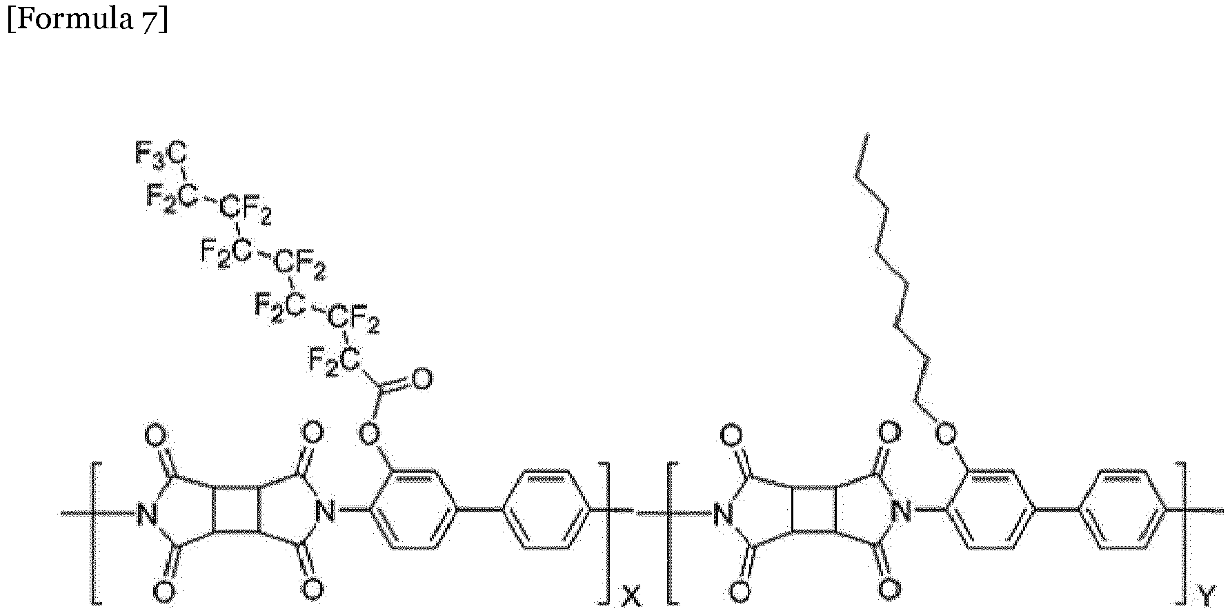
(Table 1) Contact angles (degrees) w/ H2O Numbers of CF2 (CF3) Carbon Number Nos. 0 Nos. 3 Nos. 4 Nos. 5 Nos. 7 Nos. 9 Nos. 11 Nos. 13 Nos. 15 8 74 80 86 86 90 10 76 76 80 84 94 104 - 12 78 82 86 94 100 102 108 14 82 86 94 100 104 108 110 114 16 92 92 98 100 110 110 112 116 116 (Table 2) Contact angles (degrees) w/ H2O Numbers of CF2 (CF3) Carbon Number Nos. 0 Nos. 3 Nos. 4 Nos. 5 Nos. 7 Nos. 9 Nos. 11 Nos. 13 Nos. 15 8 76 80 84 88 90 10 76 76 80 92 94 104 12 78 82 90 100 102 102 108 14 82 94 94 104 104 108 112 114 16 92 92 98 108 112 114 116 116 116 (Table 3) Contact angles (degrees) w/ H2O Numbers of CF2 (CF3) Carbon Number Nos. 0 Nos. 3 Nos. 4 Nos. 5 Nos. 7 Nos. 9 Nos. 11 Nos. 13 Nos. 15 8 74 78 84 90 92 10 70 76 80 94 96 106 12 76 82 86 94 100 102 110 14 78 86 94 104 104 108 112 116 16 82 90 98 108 112 114 116 116 116 - Referring to Table 1 to Table 3, it is determined that, when CF2 or CF3 is o and the carbon number is equal to or greater than 14, the contact angle is equal to or greater than 80 degrees.
- According to example embodiments, the main chain may comprise a compound represented by Formula 8 or Formula 9:


- In Formula 8 and Formula 9, X and Y may be 1 to 10,000, and a sum of m and n may be equal to or greater than 8. Further, the R' may be one of -H, alkyl, aromatic, OCO alkyl, or OCO halogen.
- A display device according to another example embodiment will now be described.
- A display device according to the present example embodiment may correspond to the above-described example embodiments except that the
side chain 20 of thepartition wall 380 according to the present example embodiment comprises fluorine. Repeated description of details that are the same as the above-described constituent elements may be omitted for clarity. - According to the present example embodiment, the
side chain 20 comprises fluorine, and the carbon number of the side chain may be equal to or greater than 8. Theside chain 20 comprises fluorine, and thus when the carbon number of the side chain is less than the above-described example embodiment, the partition wall may still exhibit a contact angle that is equal to or greater than 80 degrees. For example, the side chain may comprise at least eight fluorine atoms. - In the present example embodiment, the
side chain 20 may be formed by a reaction of one or more of Formulae 5-1 to 5-5:


- In Formulae 5-1 to 5-5, m1 and n1 may independently be an integer that is equal to or less than 30, n2 may be an integer of 5 to 30, m3 and n3 may independently be an integer that is equal to or less than 30, a sum of m3 and n3 may be equal to or greater than 2, n4 may be an integer of 6 to 30, X may be one of

- Description of the
main chain 10 corresponds to the above-described example embodiments. Themain chain 10 may be a polyimide-based polymer. For example, themain chain 10 may be a reaction product of a dianhydride compound and a diamine compound. - For example, the
main chain 10 may be a reaction product of at least one compound from among Formulae 1-1 to 1-6 and at least one compound from among Formulae 2-1 to 2-6.
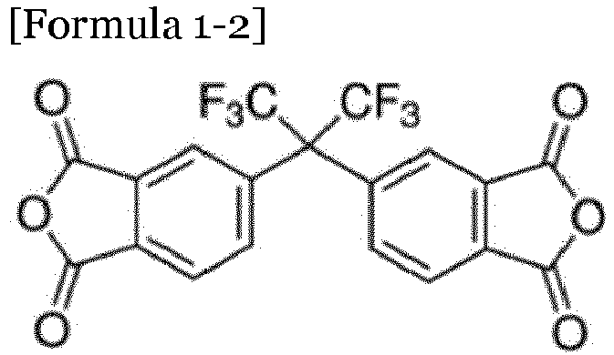




- In an example embodiment, the partition wall may have a structure represented by, for example, Formula B:

- Referring to Formula B, the partition wall comprises a side chain connected to the main chain, and the side chain comprises fluorine. A partition wall formed using Formula B may have an enhanced hydrophobic property because of the side chain comprising fluorine.
- The partition wall may comprise an addition product of an additive 30. The additive 30 may comprise fluorine. The additive 30 may comprise at least one reactive group from among an acryl group, a methacryl group, an epoxy group, or a maleimide group that may react with the
main chain 10. The additive 30 may be connected in a side chain form to themain chain 10 through the reactive group. - The additive 30 may be, for example, one or more of Formulae 3-1 to 3-6:


- In Formulae 3-1 to 3-6, m1 and n1 may independently be an integer that is equal to or less than 30, n2 may be an integer of 1 to 30, m3 and n3 may independently be an integer that is equal to or less than 30, and n4 may be an integer of 1 to 30.
- Some of the compounds of Formulae 3-1 to 3-6, which are examples of the additive 30, have a similar structure to the side chain. Thus, in the present example embodiment in which the
side chain 20 comprises fluorine, the additive 30 may not be substantially similar to theside chain 20. Thepartition wall 380 may further comprise one or more of an initiator, a crosslinking agent, a photoactive compound, or a surfactant. - Referring to Table 1 to Table 3, when CF2 or CF3 is equal to or greater than 4, it is determined that the contact angle is equal to or greater than 80 degrees when the carbon number is equal to or greater than 8. Thus, the above-described example embodiment shows the hydrophobic property exhibiting the contact angle that is equal to or greater than 80 degrees when the fluorine number is 0 and the carbon number is equal to or greater than 14, and the partition wall composition according to the present example embodiment comprises fluorine, so it has the hydrophobic property that has the contact angle that is equal to or greater than 80 degrees when the carbon number is equal to or greater than 8.
- A process for manufacturing a partition wall composition according to an example embodiment will now be described.
- In the synthesis method described below, a
side chain 20 or an additive 30 is connected to amain chain 10. - A reaction for connecting the
side chain 20 to themain chain 10 may be given as Reaction Formula 1:
- In Reaction Formula 1, R'OH is a main chain, and RCOOH is a side chain or an additive.
- When a thick sulfuric acid exists as a catalyst, RCOOH and R'OH generate an esterification reaction. In this instance, a mole ratio of RCOOH and R'OH may be 2:1, for example. The reaction may be reversible and slow, and it may be performed slowly for about two hours or more at room temperature. When the reacted solution is precipitated in methanol, a product that has undergone an esterification reaction is precipitated. When the precipitated polymer is dried, a side chain connected to a main chain may be generated. In this instance, it is possible to control a reaction rate of the side chain by controlling a content of the side chain material (RCOOH). For example, 3 mM of R'OH may be comprised, and 6 mM of RCOOH maybe comprised.
- In an example embodiment, the R'OH (the main chain) may be a compound represented by Formula A, and the RCOOH (the side chain) may be a compound represented by Formula C, for example.


- A display device comprising a partition wall according to an example embodiment will now be described in detail with reference to drawings.
-
FIG. 5 shows a top plan view of a display device according to an example embodiment.FIG. 6 shows a cross-sectional view with respect to a line VI-VI' ofFIG. 5 . - The drawings show a 2Tr-1Cap-structured active-matrix (AM) emissive display device comprising two thin film transistors (TFTs) T1 and T2 and a capacitor C1 at each pixel of a display area, but this is merely an example.
- In an example embodiment, in the emissive display device, one pixel may comprise at least three transistors and at least two capacitors, and additional wires may be further comprised to have various configurations. Here, the pixel represents a minimum unit for displaying an image, and a display area displays an image through a plurality of pixels.
- Referring to
FIG. 5 andFIG. 6 , the emissive display device according to the present example embodiment comprises a switching thin film transistor T1, a driving thin film transistor T2, a capacitor C1, and a light-emitting device E1 respectively formed on a plurality of pixels provided on asubstrate 110. Agate line 121 disposed in one direction, and adata line 171 and acommon power line 172 crossing thegate line 121 in an insulating manner, are provided on thesubstrate 110. Here, the pixel may be defined by thegate line 121, thedata line 171, and thecommon power line 172 as borders, for example. - The light emitting element E1 comprises a
first electrode 191, a light-emittingdevice layer 370 formed on thefirst electrode 191, and asecond electrode 270 formed on the light-emittingdevice layer 370. - Here, the
first electrode 191 is an anode that is a hole injection electrode, and thesecond electrode 270 is a cathode that is an electron injection electrode. However, thefirst electrode 191 may be a cathode and thesecond electrode 270 may be an anode depending on the method for driving an emissive display device. Thefirst electrode 191 may be a pixel electrode, and thesecond electrode 270 may be a common electrode. - The light-emitting
device layer 370 may comprise one or more of a hole injection layer, a hole transfer layer, an emission layer, an electron transfer layer, or an electron injection layer. The emission layer may comprise an organic emission layer, and light emits when excitons that are generated when the injected holes and electrons are combined enter a ground state from an excited state. In another implementation, the emission layer may comprise a quantum dot.
In case of the emission layer comprise an organic emission layer, the emission layer may comprise blue, red, or green light emitting materials, and may further comprise a host and a dopant. The materials comprised in the emission layer are not limited. For example, the emission layer may comprise blue emitting materials such as oxadiazole dimer dyes (e.g., bis-DAPOXP), spiro compounds (e.g., spiro-DPVBi, spiro-6P), triarylamine compounds, bis(styryl)amine compounds (e.g., DPVBi, DSA), 4,4'-bis(9-ethyl-3-carbazovinylene)-1,1'-biphenyl (BCzVBi), perylene, 2,5,8,11-tetra-tert-butyl perylene (TPBe), 9H-carbazol-3,3'-(1,4-phenylene-di-2,1-ethene-diyl)bis[9-ethyl-9C] (BCzVB), 4,4-bis[4-(di-p-tolylamino)styryl]biphenyl (DPAVBi), 4-(di-p-tolylamino)-4'-[(di-p-tolylamino)styryl] stilbene (DPAVB), 4,4'-bis[4-(diphenylamino)styryl]biphenyl (BDAVBi), bis(3,5-difluoro-2-(2-pyridyl)phenyl-(2-carboxypyridyl)iridium(III) (FIrPic), and/or the like; green emitting materials such as 3-(2-benzothiazolyl)-7-(diethylamino)coumarin (Coumarin 6), 2,3,6,7-tetrahydro-1,1,7,7,-tetramethyl-1H,5H,11H-10-(2-benzothiazolyl)quinolizino-[9,9a,1gh]coumarin (C545T), N,N'-dimethyl-quinacridone (DMQA), tris(2-phenylpyridine)iridium(III) (Ir(ppy)3), and/or the like; and red emitting materials such as tetraphenylnaphthacene (Rubrene), tris(1-phenylisoquinoline)iridium(III) (Ir(piq)3), bis(2-benzo[b]thiophen-2-yl-pyridine), (acetylacetonate)iridium(III) (Ir(btp)2(acac)), tris(dibenzoylmethane)phenanthroline europium(III) (Eu(dbm)3(phen)), a tris[4,4'-di-tert-butyl-(2,2')-bipyridine]ruthenium(III) complex (Ru(dtb-bpy)3 ∗2 PF6), DCM1, DCM2, Eu(thenoyltrifluoroacetone)3 (Eu(TTA)3, butyl-6-(1,1,7,7-tetramethyljulolidyl-9-enyl)-4H-pyran: (DCJTB), and/or the like. Furthermore, a light emitting polymer material may be included. For example a polymer such as phenylene, poly(p-phenylene vinylene), thiophene, fluorene, spiro-fluorene, and/or the like, or an aromatic compound comprising nitrogen and/or the like may be included, but embodiments are not limited thereto. The emission layer may be manufactured by additionally doping a light emitting dopant into an emission layer host. Non-limiting examples of fluorescent light emitting host materials may include tris(8-hydroxy-quinolinato)aluminum (Alq3), 9,10-di(naphth-2-yl)anthracene (AND), 3-tert-butyl-9,10-di(naphth-2-yl)anthracene (TBADN), 4,4'-bis(2,2-diphenyl-ethene-1-yl)-4,4'-dimethylphenyl (DPVBi), 4,4'-bis(2,2-diphenyl-ethene-1-yl)-4,4'-methylphenyl (p-DMDPVBi), ter(9,9-diarylfluorene)s (TDAFs), 2-(9,9'-spirobifluorene-2-yl)-9,9'-spirobifluorene (BSDF), 2,7-bis(9,9'-spirobifluorene-2-yl)-9,9'-spirobifluorene (TSDF), bis(9,9-diarylfluorene)s (BDAFs), 4,4'-bis(2,2-diphenyl-ethene-1-yl)-4,4'-di-(tert-butyl)phenyl (p-TDPVBi),and/ or the like, and non-limiting examples of phosphorescent host materials may include 1,3-bis(carbazole-9-yl)benzene (mCP), 1,3,5-tris(carbazole-9-yl)benzene (tCP), 4,4',4"-tris(carbazole-9-yl)triphenylamine (TcTa), 4,4'-bis(carbazole-9-yl)biphenyl (CBP), 4,4'-bis(9-carbazolyl)-2,2'-dimethyl-biphenyl (CBDP), 4,4'-bis(carbazole-9-yl)-9,9-dimethyl-fluorene (DMFL-CBP), 4,4'-bis(carbazole-9-yl)-9,9-bis(9-phenyl-9H-carbazole)fluorene (FL-4CBP), 4,4'-bis(carbazole-9-yl)-9,9-di-tolyl-fluorene (DPFL-CBP), 9,9-bis(9-phenyl-9H-carbazole)fluorene (FL-2CBP), and/or the like. - The content of the light emitting dopant may vary according to the material forming the emission layer, but generally, the content of the light emitting dopant may be in a range of about 3 to about 10 parts by weight based on 100 parts by weight of the material forming the emission layer (total weight of the host and the dopant). In case of the emission layer comprise a quantum dot, a core of the quantum dot may be selected from among a group II-VI compound, a group III-V compound, a group IV-VI compound, a group IV element, a group IV compound, and a combination thereof.
- The group II-VI compound may be selected from among a binary compound selected from among CdSe, CdTe, ZnS, ZnSe, ZnTe, ZnO, HgS, HgSe, HgTe, MgSe, MgS, and a mixture thereof; a tertiary compound selected from among AgInS, CuInS, CdSeS, CdSeTe, CdSTe, ZnSeS, ZnSeTe, ZnSTe, HgSeS, HgSeTe, HgSTe, CdZnS, CdZnSe, CdZnTe, CdHgS, CdHgSe, CdHgTe, HgZnS, HgZnSe, HgZnTe, MgZnSe, MgZnS, and a mixture thereof; and a quaternary compound selected from among HgZnTeS, CdZnSeS, CdZnSeTe, CdZnSTe, CdHgSeS, CdHgSeTe, CdHgSTe, HgZnSeS, HgZnSeTe, HgZnSTe, and a mixture thereof.
- The group III-V compound may be selected from among a binary compound selected from among GaN, GaP, GaAs, GaSb, AlN, AlP, AlAs, AlSb, InN, InP, InAs, InSb, and a mixture thereof; a tertiary compound selected from among GaNP, GaNAs, GaNSb, GaPAs, GaPSb, AlNP, AlNAs, AlNSb, AlPAs, AlPSb, InGaP, InNP, InNAs, InNSb, InPAs, InPSb, GaAlNP, and a mixture thereof; and a quaternary compound selected from among GaAlNAs, GaAlNSb, GaAlPAs, GaAlPSb, GaInNP, GaInNAs, GaInNSb, GaInPAs, GaInPSb, InAlNP, InAlNAs, InAlNSb, InAlPAs, InAlPSb, and a mixture thereof.
- The group IV-VI compound may be selected from among a binary compound selected from among SnS, SnSe, SnTe, PbS, PbSe, PbTe, and a mixture thereof; a tertiary compound selected from among SnSeS, SnSeTe, SnSTe, PbSeS, PbSeTe, PbSTe, SnPbS, SnPbSe, SnPbTe, and a mixture thereof; and a quaternary compound selected from among SnPbSSe, SnPbSeTe, SnPbSTe, and a mixture thereof. The group IV element may be selected from among SI, Ge, and a mixture thereof. The group IV compound may be a binary compound selected from among SiC, SiGe, and a mixture thereof.
- In this instance, the binary compound, the tertiary compound, or the quaternary compound may exist in particles at a uniform concentration, or may exist in the same particle divided into states where concentration distributions partially differ. Further, the color conversion media layer may have a core/shell structure where one quantum dot surrounds another quantum dot. An interface between the core and the shell may have a concentration gradient such that a concentration of an element existing in the shell is gradually reduced nearing the center thereof.
- In several exemplary embodiments, the quantum dot may have a core-shell configuration comprising a core comprising the nanocrystal and a shell surrounding the core. The shell of the quantum dot may function as a passivation layer for maintaining a semiconductor characteristic by preventing a chemical change of the core and/or function as a charging layer for assigning an electrophoretic characteristic to the quantum dot. The shell may be a single layer or a multilayer. An interface of the core and the shell may have a gradient of concentration in which the concentration of the element existing in the shell reduces as it approaches the center. An example of the shell of the quantum dot comprises an oxide of a metal or a non-metal, a semiconductor compound, or a combination thereof.
- For example, the oxide of a metal or a non-metal may exemplify a binary compound such as SiO2, Al2O3, TiO2, ZnO, MnO, Mn2O3, Mn3O4, CuO, FeO, Fe2O3, Fe3O4, CoO, Co3O4, and NiO or a tertiary compound such as MgAl2O4, CoFe2O4, NiFe2O4, and CoMn2O4, and the present exemplary embodiment is not limited thereto.
- The semiconductor compound may exemplify CdS, CdSe, CdTe, ZnS, ZnSe, ZnTe, ZnSeS, ZnTeS, GaAs, GaP, GaSb, HgS, HgSe, HgTe, InAs, InP, InGaP, InSb, AlAs, AlP, AlSb, and the present exemplary embodiment is not limited thereto.
- The quantum dot may have a full width at half maximum (FWHM) of an emission wavelength spectrum of about 45 nm or less, preferably about 40 nm or less, and more preferably about 30 nm or less, and in this range, color purity or color reproducibility may be improved.
- Also, the light emitted through the quantum dot is irradiated in all directions, thereby improving a light viewing angle.
- Further, the form of the quantum dot is one generally used in the art and is not particularly limited, but more specifically, it may be formed to be spherical, pyramidal, multi-armed, or cubic nanoparticles, nanotubes, nanowires, nanofibers, and nanoplate-shaped particles.
- The quantum dot may control the colors of light emitted according to a size of particles, and the quantum dot may accordingly have various emitting colors such as red, green, and blue.
- The capacitor C1 comprises a pair of
capacitive plates layer 160 therebetween. Here, theinterlayer insulating layer 160 is a dielectric material. Capacitance is determined by charges stored in the capacitor C1 and a voltage between a pair ofcapacitive plates - The switching thin film transistor T1 comprises a switching
semiconductor layer 151, a switching gate electrode 122, a switching source electrode 176, and aswitching drain electrode 177. The driving thin film transistor T2 comprises a drivingsemiconductor layer 155, a drivinggate electrode 124, a drivingsource electrode 173, and a drivingdrain electrode 175. - The switching thin film transistor T1 is used as a switching element for selecting a pixel to emit. The switching gate electrode 122 is connected to the
gate line 121, and the switching source electrode 176 is connected to thedata line 171. The switchingdrain electrode 177 is separately disposed from the switching source electrode 176 and is connected to onecapacitive plate 158. - The driving thin film transistor T2 applies driving power for emitting the light-emitting
device layer 370 of the light emitting element E1 in the selected pixel to thefirst electrode 191. The drivinggate electrode 124 is connected to thecapacitive plate 158 connected to theswitching drain electrode 177. The drivingsource electrode 173 and theother capacitive plate 178 are respectively connected to thecommon power line 172. - The driving
drain electrode 175 is connected to thefirst electrode 191 through acontact hole 185. - An light emitting device according to an example embodiment will now be described in detail with reference to
FIG. 5 andFIG. 6 . - In the present example embodiment, a
buffer layer 111 is provided on thesubstrate 110. Thesubstrate 110 may be made of glass, quartz, ceramic, or plastic. Thebuffer layer 111 may be made of a silicon nitride (SiNy), a silicon oxide (SiO2), a silicon oxynitride (SiOxNy), etc. The x and y may respectively be 1 to 5, for example. - In the present example embodiment, a driving
semiconductor layer 155 is formed on thebuffer layer 111. The drivingsemiconductor layer 155 may be made of various semiconductor materials such as a polysilicon film or an amorphous silicon film. The drivingsemiconductor layer 155 may comprise a source region 152, a channel region 153, and a drain region 154. - In the present example embodiment, a
gate insulating layer 140 made of a silicon nitride or a silicon oxide is provided on the drivingsemiconductor layer 155. A drivinggate electrode 124 and afirst capacitive plate 158 are provided on thegate insulating layer 140. In this instance, the drivinggate electrode 124 overlaps at least a portion of the drivingsemiconductor layer 155, in detail, the channel region 153. - In the present example embodiment, an
interlayer insulating layer 160 covering the drivinggate electrode 124 is provided on thegate insulating layer 140. The interlayer insulatinglayer 160 may be formed of a silicon nitride or a silicon oxide in a like manner of thegate insulating layer 140. Thegate insulating layer 140 and the interlayer insulatinglayer 160 have afirst contact hole 163 and asecond contact hole 165 for exposing a source region 152 and a drain region 154 of the drivingsemiconductor layer 155. - In the present example embodiment, a driving
source electrode 173, a drivingdrain electrode 175, adata line 171, acommon power line 172, and asecond capacitive plate 178 are provided on theinterlayer insulating layer 160. The drivingsource electrode 173 and the drivingdrain electrode 175 are connected to the source region 152 and the drain region 154 of the drivingsemiconductor layer 155 through thefirst contact hole 163 and thesecond contact hole 165. - In the present example embodiment, an insulating
layer 180 for covering the drivingsource electrode 173 and the drivingdrain electrode 175 is provided on theinterlayer insulating layer 160. The insulatinglayer 180 may comprise an organic material such as a polyacryl or a polyimide. - In the present example embodiment, the insulating
layer 180 comprises acontact hole 185. Thefirst electrode 191 is provided on the insulatinglayer 180. Thefirst electrode 191 may be a pixel electrode. Thefirst electrode 191 is connected to the drivingdrain electrode 175 through thecontact hole 185. - In the present example embodiment, the
partition wall 380 is provided on the insulatinglayer 180. The description on thepartition wall 380 corresponds to the above-provided descriptions of example embodiments. Thus, thepartition wall 380 may comprise a main chain and a side chain connected to the main chain, the carbon number of the side chain may be 14, and the contact angle of the partition wall may be equal to or greater than 80 degrees. In another implementation, thepartition wall 380 may comprise a main chain and a side chain connected to the main chain, the side chain may comprise fluorine, the carbon number of the side chain may be equal to or greater than 8, and the contact angle of the partition wall may be equal to or greater than 80 degrees. In this instance, the number of the fluorine atoms of the side chain may be equal to or greater than 8. Further, the partition wall may further comprise an addition product of an additive comprising fluorine. The additive may comprise at least one reactive group from among the acryl group, the methacryl group, the epoxy group, or the maleimide group that may react with the main chain, and the additive may be connected in a side chain form to the main chain through the reactive group. The partition wall may further comprise one or more of the initiator, the crosslinking agent, the photoactive compound, or the surfactant. Detailed descriptions of the main chain, the side chain, and the additive of thepartition wall 380 correspond to the above-provided descriptions. - In the present example embodiment, the light-emitting
device layer 370 is provided to overlap thefirst electrode 191, and thesecond electrode 270 is provided to overlap the light-emittingdevice layer 370. The light-emittingdevice layer 370 may comprise one or more of the hole injection layer, the hole transfer layer, the emission layer, the electron transfer layer, or the electron injection layer. Thesecond electrode 270 may be a common electrode. The light-emitting device E1 comprises afirst electrode 191, a light-emittingdevice layer 370, and asecond electrode 270. - The
partition wall 380 of the display device according to the present example embodiment comprises amain chain 10 and aside chain 20 connected thereto. When the carbon number of the side chain is equal to or greater than 14, the side chain may not contain fluorine and thepartition wall 380 may be hydrophobic without fluorine in the side chain, and thepartition wall 380 may have the contact angle that is equal to or greater than 80 degrees. Further, when the side chain comprises fluorine, thepartition wall 380 may have the contact angle that is equal to or greater than 80 degrees when the carbon number is equal to or greater than 8. - The
partition wall 380 with an excellent hydrophobic property by the side chain may prevent theinkjet material 371 from overflowing thepartition wall 380 when the light-emittingdevice layer 370 is formed by the inkjet, and may efficiently form the light-emittingdevice layer 370. -
FIG. 7 shows a display device according to another exemplary embodiment of the present invention. Referring toFIG. 7 , the display device corresponds to the display device described with reference toFIG. 6 except for the configuration of acolor converting panel 200. No description on the same configurational elements will be provided, - The emission layer of the light-emitting
device layer 370 may emit blue light. The blue light passes through thecolor converting layer 330 of thecolor converting panel 200 to be converted to red or green light or transmitted as blue through the converting layer. - Regarding the
color converting panel 200, Acolor filter 230 is provided on asecond substrate 210. Here, thecolor filter 230 is provided between thefirst substrate 110 and thesecond substrate 210. Alight blocking member 220 is provided between thecolor filter 230 and thesecond substrate 210, and thelight blocking member 220 may partly overlap thecolor filter 230. - A color
filter insulating layer 250 is provided on thecolor filter 230 and thelight blocking member 220. Acolor converting layer 330 is provided on the colorfilter insulating layer 250. That is, the colorfilter insulating layer 250 is provided between thecolor converting layer 330 and thecolor filter 230. Thecolor converting layer 330 may be provided to overlap thecolor filter 230. - The
color converting layer 330 comprises a quantum dot and converts incident light into another color of light. A description on the quantum dot corresponds to the above-provided description. Thecolor converting layer 330 may comprise a green color converting layer, a red color converting layer, and a blue color converting layer, and it may convert the blue light emitted by the light-emittingdevice layer 370 into green light or red light or transmit the blue light. - An
encapsulation layer 390 may be provided between thecolor converting panel 200 and thesecond electrode 270. - That is, regarding the display device according to an exemplary embodiment of
FIG. 7 , the display panel comprising a light-emittingdevice layer 370 and thecolor converting panel 200 comprising acolor converting layer 330 are combined. The light-emittingdevice layer 370 may emit blue light. The blue light passes through thecolor converting layer 330 and is converted into red light or green light by the respective color converting layers or is transmitted as blue light by the transmission layer. - The light having transmitted through the
color converting layer 330 passes through the respective color filters, and color purity is improved. In addition, thecolor filter 230 is prevented to not generate a color conversion on thecolor converting layer 330 by light input from the outside. - By way of summation and review, when droplets are discharged through the inkjet printing device to form a film, a shape attached to a substrate in an earlier stage may be changed according to surface energy between the ink and the substrate to be printed. In the case of an emission layer, if an emission layer is not correctly formed on a bank wall, an electrical short circuit may be generated, and/or a thickness of the emission layer may not be uniform so that brightness may not be uniform and a lifespan may be reduced. Further, when discharged droplets flow not inside but outside the bank, a short circuit may be generated or efficiency may be deteriorated.
- As described above, embodiments relate to a display device with a partition wall comprising a main chain and a side chain and having a hydrophobic property. Embodiments may provide a display device comprising a hydrophobic partition wall that comprises a main chain and a side chain connected thereto, and having a contact angle that is equal to or greater than 80 degrees. The present invention has been made in an effort to provide a display device for efficiently forming a light-emitting device layer by an inkjet process when a partition wall is hydrophobic. According to the example embodiments, the display device has a hydrophobic partition wall, thereby efficiently forming the light-emitting device layer according to the inkjet process.
- Example embodiments have been disclosed herein, and although specific terms are employed, they are used and are to be interpreted in a generic and descriptive sense only and not for purpose of limitation. In some instances, as would be apparent to one of ordinary skill in the art as of the filing of the present application, features, characteristics, and/or elements described in connection with a particular embodiment may be used singly or in combination with features, characteristics, and/or elements described in connection with other embodiments unless otherwise specifically indicated. Accordingly, it will be understood by those of skill in the art that various changes in form and details may be made without departing from the spirit and scope of the present invention as set forth in the following claims.
Claims (15)
- A display device, comprising:a substrate;a thin film transistor provided on the substrate;a first electrode connected to the thin film transistor;a second electrode overlapping the first electrode; anda partition wall comprising a partition wall composition and a light-emitting device layer provided between the first electrode and the second electrode, wherein:the partition wall composition comprises a main chain and a side chain connected to the main chain, anda carbon number of the side chain is equal to or greater than 14.
- The display device as claimed in claim 1, wherein the main chain is a reaction product of a dianhydride compound and a diamine compound.
- The display device as claimed in claim 1, wherein the main chain is a reaction product of at least one compound from among Formulae 1-1 to 1-6 and at least one compound from among Formulae 2-1 to 2-6:


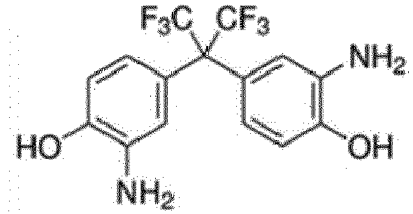
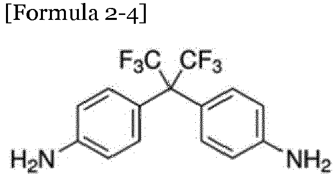


- The display device as claimed in claim 1, wherein the side chain comprises fluorine.
- The display device as claimed in claim 1, wherein:
the partition wall composition comprises an addition product of an additive and the main chain, wherein the additive comprises fluorine, and at least one reactive group from among an acryl group, a methacryl group, an epoxy group, and a maleimide group that may react with the main chain. - The display device as claimed in claim 5, wherein the addition product of the additive and the main chain comprises a covalent bond formed between a portion derived from the additive and the main chain.
- The display device as claimed in claim 1, wherein:
the partition wall composition comprises an addition product of the main chain and an additive which is one or more of Formulae 3-1 to 3-6:


- The display device as claimed in claim 1, wherein the side chain is provided by a compound represented by Formula 4:


the l is equal to or greater than 13. - The display device as claimed in claim 1, wherein the partition wall composition comprises a reaction product of the main chain and one or more of an initiator, a crosslinking agent, a photoactive compound, or a surfactant.
- The display device of claim 1, wherein
the light-emitting device layer further comprises an emission layer, and the emission layer comprises a quantum dot material. - A display device, comprising:a substrate;a thin film transistor provided on the substrate;a first electrode connected to the thin film transistor;a second electrode overlapping the first electrode; anda partition wall comprising a partition wall composition and a light-emitting device layer provided between the first electrode and the second electrode, wherein:wherein the partition wall composition comprises a main chain and a side chain connected to the main chain,the side chain comprises fluorine, anda carbon number of the side chain is equal to or greater than 8.
- The display device as claimed in claim 11, wherein the side chain comprises a number of fluorine atoms that is equal to or greater than 8.
- The display device as claimed in claim 11, wherein the side chain is provided by one or more compound of Formulae 5-1 to 5-5:


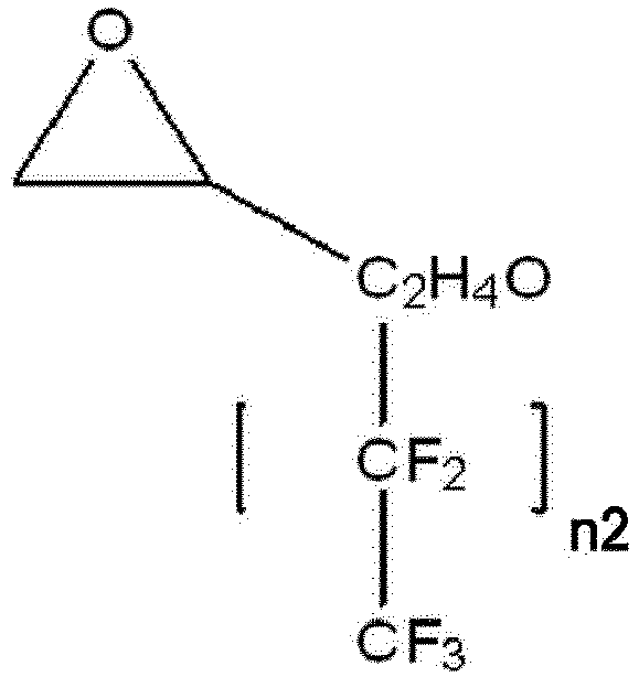


wherein,m1 and n1 are independently an integer that is equal to or less than 30,n2 is an integer of 5 to 30,m3 and n3 are independently an integer that is equal to or less than 30, provided that a sum of the m3 and n3 is equal to or greater than 2,n4 is an integer of 6 to 30,n5 is equal to or greater than 7, andX is one of
- The display device as claimed in claim 11, wherein the main chain is a reaction product of at least one compound from among Formulae 1-1 to 1-6 and at least one compound from among Formulae 2-1 to 2-6:


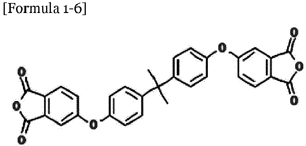


- The display device of claim 11, wherein
the light-emitting device layer further comprises an emission layer, and the emission layer comprises a quantum dot material.
Applications Claiming Priority (2)
| Application Number | Priority Date | Filing Date | Title |
|---|---|---|---|
| KR20180054709 | 2018-05-14 | ||
| KR1020190041435A KR102776376B1 (en) | 2018-05-14 | 2019-04-09 | Display device |
Publications (2)
| Publication Number | Publication Date |
|---|---|
| EP3570329A1 true EP3570329A1 (en) | 2019-11-20 |
| EP3570329B1 EP3570329B1 (en) | 2022-12-14 |
Family
ID=66542042
Family Applications (1)
| Application Number | Title | Priority Date | Filing Date |
|---|---|---|---|
| EP19174211.3A Active EP3570329B1 (en) | 2018-05-14 | 2019-05-13 | Display device |
Country Status (3)
| Country | Link |
|---|---|
| US (1) | US11264437B2 (en) |
| EP (1) | EP3570329B1 (en) |
| CN (1) | CN110491903B (en) |
Families Citing this family (2)
| Publication number | Priority date | Publication date | Assignee | Title |
|---|---|---|---|---|
| KR102661411B1 (en) * | 2018-12-28 | 2024-04-25 | 엘지디스플레이 주식회사 | Organic light emitting diode and orgnic light emitting device including the same |
| US12454644B2 (en) * | 2020-06-04 | 2025-10-28 | Sharp Kabushiki Kaisha | Display device and method for producing display device |
Citations (2)
| Publication number | Priority date | Publication date | Assignee | Title |
|---|---|---|---|---|
| JP2007324033A (en) * | 2006-06-02 | 2007-12-13 | Casio Comput Co Ltd | Display device and manufacturing method thereof |
| WO2011081151A1 (en) * | 2009-12-28 | 2011-07-07 | 旭硝子株式会社 | Photosensitive composition, partition wall, color filter and organic el element |
Family Cites Families (22)
| Publication number | Priority date | Publication date | Assignee | Title |
|---|---|---|---|---|
| CN100403355C (en) | 1996-09-19 | 2008-07-16 | 精工爱普生株式会社 | Matrix display element and manufacturing method thereof |
| JP3899566B2 (en) | 1996-11-25 | 2007-03-28 | セイコーエプソン株式会社 | Manufacturing method of organic EL display device |
| JP3580092B2 (en) | 1997-08-21 | 2004-10-20 | セイコーエプソン株式会社 | Active matrix display |
| EP1505648A3 (en) | 1997-08-21 | 2005-08-10 | Seiko Epson Corporation | Active matrix display device |
| WO1999048339A1 (en) | 1998-03-17 | 1999-09-23 | Seiko Epson Corporation | Substrate for patterning thin film and surface treatment thereof |
| JP3646510B2 (en) | 1998-03-18 | 2005-05-11 | セイコーエプソン株式会社 | Thin film forming method, display device, and color filter |
| JP2000206509A (en) * | 1999-01-19 | 2000-07-28 | Alps Electric Co Ltd | Tft type liquid crystal display device |
| TW480722B (en) | 1999-10-12 | 2002-03-21 | Semiconductor Energy Lab | Manufacturing method of electro-optical device |
| KR100834344B1 (en) | 2001-12-29 | 2008-06-02 | 엘지디스플레이 주식회사 | Active matrix organic electroluminescent device and manufacturing method thereof |
| JP4061132B2 (en) | 2002-06-21 | 2008-03-12 | 大阪瓦斯株式会社 | Fluorine-containing polysilane compound |
| GB2391686B (en) | 2002-07-31 | 2006-03-22 | Dainippon Printing Co Ltd | Electroluminescent display and process for producing the same |
| AU2003260959A1 (en) | 2002-09-11 | 2004-04-30 | Semiconductor Energy Laboratory Co., Ltd. | Light-emitting apparatus and fabrication method of the same |
| JP5572942B2 (en) * | 2008-11-28 | 2014-08-20 | 住友化学株式会社 | Light emitting device and manufacturing method thereof |
| WO2011014216A1 (en) | 2009-07-27 | 2011-02-03 | E. I. Du Pont De Nemours And Company | Process and materials for making contained layers and devices made with same |
| JP5428657B2 (en) | 2009-08-31 | 2014-02-26 | ダイキン工業株式会社 | Liquid repellent-topcoat composition for lyophilic patterning |
| JP5622564B2 (en) | 2010-06-30 | 2014-11-12 | 富士フイルム株式会社 | Photosensitive composition, pattern forming material, and photosensitive film using the same, pattern forming method, pattern film, low refractive index film, optical device, and solid-state imaging device |
| KR101888941B1 (en) | 2012-05-16 | 2018-08-16 | 엘지디스플레이 주식회사 | Display device and method of manufacturing the same |
| KR20140067645A (en) | 2012-11-27 | 2014-06-05 | 엘지디스플레이 주식회사 | Organic electro-luminescent device and method of fabricating the same |
| KR102510370B1 (en) * | 2014-10-06 | 2023-03-17 | 도레이 카부시키가이샤 | Resin composition, method for producing heat-resistant resin film, and display device |
| KR102464613B1 (en) | 2015-04-30 | 2022-11-08 | 엘지디스플레이 주식회사 | Organic light emitting display device and method of fabricating the same |
| US10712483B2 (en) * | 2015-08-24 | 2020-07-14 | Samsung Electronics Co., Ltd. | Photosensitive compositions, quantum dot polymer composite pattern prepared therefrom, and electronic devices including the same |
| KR102478491B1 (en) * | 2015-12-30 | 2022-12-16 | 엘지디스플레이 주식회사 | Organic Light Emitting Diode Display Device And Method Of Fabricating The Same |
-
2019
- 2019-05-13 US US16/410,115 patent/US11264437B2/en active Active
- 2019-05-13 EP EP19174211.3A patent/EP3570329B1/en active Active
- 2019-05-14 CN CN201910398675.9A patent/CN110491903B/en active Active
Patent Citations (2)
| Publication number | Priority date | Publication date | Assignee | Title |
|---|---|---|---|---|
| JP2007324033A (en) * | 2006-06-02 | 2007-12-13 | Casio Comput Co Ltd | Display device and manufacturing method thereof |
| WO2011081151A1 (en) * | 2009-12-28 | 2011-07-07 | 旭硝子株式会社 | Photosensitive composition, partition wall, color filter and organic el element |
Also Published As
| Publication number | Publication date |
|---|---|
| CN110491903A (en) | 2019-11-22 |
| EP3570329B1 (en) | 2022-12-14 |
| US20190348484A1 (en) | 2019-11-14 |
| CN110491903B (en) | 2024-08-27 |
| US11264437B2 (en) | 2022-03-01 |
Similar Documents
| Publication | Publication Date | Title |
|---|---|---|
| US20230345768A1 (en) | Display device and method of fabricating the same | |
| US20190157596A1 (en) | Quantum dot device and display device | |
| KR102696701B1 (en) | Quantum dot and lighting emitting device comprising the same | |
| KR20200019424A (en) | Quantum dot light emitting diode device | |
| US12598883B2 (en) | Display apparatus including tandem organic light-emitting diode | |
| US20180175132A1 (en) | Organic light emitting diode and organic light emitting display device including the same | |
| EP3570329B1 (en) | Display device | |
| US11744116B2 (en) | Organic light-emitting display device and method for manufacturing the same | |
| US11502136B2 (en) | Display panel | |
| KR102776376B1 (en) | Display device | |
| EP4686356A1 (en) | Light-emitting diode and display device comprising same | |
| US20250374813A1 (en) | Display device and manufacturing method thereof | |
| US20250268014A1 (en) | Display device | |
| US20250268020A1 (en) | Manufacturing method of display device | |
| US20250133950A1 (en) | Light emitting element, method for manufacturing the light emitting element, and display device comprising the light emitting element | |
| US20250107314A1 (en) | Display device and method for manufacturing the same | |
| US20250063885A1 (en) | Light emitting element, ink composition and display device including the light emitting element | |
| KR20250036307A (en) | Light emitting device, ink composition, and display device including the light emitting element | |
| KR20250107989A (en) | Display apparatus and method for manufacturing the same | |
| KR20250149550A (en) | Display device, electronic device and method for manufacturing display device | |
| KR20240141892A (en) | Ink composition, light emitting device made of the ink composition, and manufacturing method of the light emitting device | |
| CN122003066A (en) | Display devices and electronic devices including display devices | |
| CN120787057A (en) | Display device and electronic device | |
| KR20230103626A (en) | Display device | |
| CN120051178A (en) | Thin film and preparation method thereof, photoelectric device and preparation method thereof, and display device |
Legal Events
| Date | Code | Title | Description |
|---|---|---|---|
| PUAI | Public reference made under article 153(3) epc to a published international application that has entered the european phase |
Free format text: ORIGINAL CODE: 0009012 |
|
| STAA | Information on the status of an ep patent application or granted ep patent |
Free format text: STATUS: THE APPLICATION HAS BEEN PUBLISHED |
|
| AK | Designated contracting states |
Kind code of ref document: A1 Designated state(s): AL AT BE BG CH CY CZ DE DK EE ES FI FR GB GR HR HU IE IS IT LI LT LU LV MC MK MT NL NO PL PT RO RS SE SI SK SM TR |
|
| AX | Request for extension of the european patent |
Extension state: BA ME |
|
| STAA | Information on the status of an ep patent application or granted ep patent |
Free format text: STATUS: REQUEST FOR EXAMINATION WAS MADE |
|
| 17P | Request for examination filed |
Effective date: 20200520 |
|
| RBV | Designated contracting states (corrected) |
Designated state(s): AL AT BE BG CH CY CZ DE DK EE ES FI FR GB GR HR HU IE IS IT LI LT LU LV MC MK MT NL NO PL PT RO RS SE SI SK SM TR |
|
| STAA | Information on the status of an ep patent application or granted ep patent |
Free format text: STATUS: EXAMINATION IS IN PROGRESS |
|
| 17Q | First examination report despatched |
Effective date: 20200928 |
|
| RAP3 | Party data changed (applicant data changed or rights of an application transferred) |
Owner name: SAMSUNG DISPLAY CO., LTD. |
|
| GRAP | Despatch of communication of intention to grant a patent |
Free format text: ORIGINAL CODE: EPIDOSNIGR1 |
|
| STAA | Information on the status of an ep patent application or granted ep patent |
Free format text: STATUS: GRANT OF PATENT IS INTENDED |
|
| INTG | Intention to grant announced |
Effective date: 20220704 |
|
| GRAS | Grant fee paid |
Free format text: ORIGINAL CODE: EPIDOSNIGR3 |
|
| GRAA | (expected) grant |
Free format text: ORIGINAL CODE: 0009210 |
|
| STAA | Information on the status of an ep patent application or granted ep patent |
Free format text: STATUS: THE PATENT HAS BEEN GRANTED |
|
| REG | Reference to a national code |
Ref country code: DE Ref legal event code: R079 Ref document number: 602019023066 Country of ref document: DE Free format text: PREVIOUS MAIN CLASS: H01L0027320000 Ipc: H10K0059000000 |
|
| AK | Designated contracting states |
Kind code of ref document: B1 Designated state(s): AL AT BE BG CH CY CZ DE DK EE ES FI FR GB GR HR HU IE IS IT LI LT LU LV MC MK MT NL NO PL PT RO RS SE SI SK SM TR |
|
| REG | Reference to a national code |
Ref country code: GB Ref legal event code: FG4D |
|
| REG | Reference to a national code |
Ref country code: CH Ref legal event code: EP |
|
| REG | Reference to a national code |
Ref country code: DE Ref legal event code: R096 Ref document number: 602019023066 Country of ref document: DE |
|
| REG | Reference to a national code |
Ref country code: IE Ref legal event code: FG4D |
|
| REG | Reference to a national code |
Ref country code: AT Ref legal event code: REF Ref document number: 1538191 Country of ref document: AT Kind code of ref document: T Effective date: 20230115 |
|
| REG | Reference to a national code |
Ref country code: LT Ref legal event code: MG9D |
|
| REG | Reference to a national code |
Ref country code: NL Ref legal event code: MP Effective date: 20221214 |
|
| PG25 | Lapsed in a contracting state [announced via postgrant information from national office to epo] |
Ref country code: SE Free format text: LAPSE BECAUSE OF FAILURE TO SUBMIT A TRANSLATION OF THE DESCRIPTION OR TO PAY THE FEE WITHIN THE PRESCRIBED TIME-LIMIT Effective date: 20221214 Ref country code: NO Free format text: LAPSE BECAUSE OF FAILURE TO SUBMIT A TRANSLATION OF THE DESCRIPTION OR TO PAY THE FEE WITHIN THE PRESCRIBED TIME-LIMIT Effective date: 20230314 Ref country code: LT Free format text: LAPSE BECAUSE OF FAILURE TO SUBMIT A TRANSLATION OF THE DESCRIPTION OR TO PAY THE FEE WITHIN THE PRESCRIBED TIME-LIMIT Effective date: 20221214 Ref country code: FI Free format text: LAPSE BECAUSE OF FAILURE TO SUBMIT A TRANSLATION OF THE DESCRIPTION OR TO PAY THE FEE WITHIN THE PRESCRIBED TIME-LIMIT Effective date: 20221214 |
|
| REG | Reference to a national code |
Ref country code: AT Ref legal event code: MK05 Ref document number: 1538191 Country of ref document: AT Kind code of ref document: T Effective date: 20221214 |
|
| PG25 | Lapsed in a contracting state [announced via postgrant information from national office to epo] |
Ref country code: RS Free format text: LAPSE BECAUSE OF FAILURE TO SUBMIT A TRANSLATION OF THE DESCRIPTION OR TO PAY THE FEE WITHIN THE PRESCRIBED TIME-LIMIT Effective date: 20221214 Ref country code: LV Free format text: LAPSE BECAUSE OF FAILURE TO SUBMIT A TRANSLATION OF THE DESCRIPTION OR TO PAY THE FEE WITHIN THE PRESCRIBED TIME-LIMIT Effective date: 20221214 Ref country code: HR Free format text: LAPSE BECAUSE OF FAILURE TO SUBMIT A TRANSLATION OF THE DESCRIPTION OR TO PAY THE FEE WITHIN THE PRESCRIBED TIME-LIMIT Effective date: 20221214 Ref country code: GR Free format text: LAPSE BECAUSE OF FAILURE TO SUBMIT A TRANSLATION OF THE DESCRIPTION OR TO PAY THE FEE WITHIN THE PRESCRIBED TIME-LIMIT Effective date: 20230315 |
|
| P01 | Opt-out of the competence of the unified patent court (upc) registered |
Effective date: 20230516 |
|
| PG25 | Lapsed in a contracting state [announced via postgrant information from national office to epo] |
Ref country code: NL Free format text: LAPSE BECAUSE OF FAILURE TO SUBMIT A TRANSLATION OF THE DESCRIPTION OR TO PAY THE FEE WITHIN THE PRESCRIBED TIME-LIMIT Effective date: 20221214 |
|
| PG25 | Lapsed in a contracting state [announced via postgrant information from national office to epo] |
Ref country code: SM Free format text: LAPSE BECAUSE OF FAILURE TO SUBMIT A TRANSLATION OF THE DESCRIPTION OR TO PAY THE FEE WITHIN THE PRESCRIBED TIME-LIMIT Effective date: 20221214 Ref country code: RO Free format text: LAPSE BECAUSE OF FAILURE TO SUBMIT A TRANSLATION OF THE DESCRIPTION OR TO PAY THE FEE WITHIN THE PRESCRIBED TIME-LIMIT Effective date: 20221214 Ref country code: PT Free format text: LAPSE BECAUSE OF FAILURE TO SUBMIT A TRANSLATION OF THE DESCRIPTION OR TO PAY THE FEE WITHIN THE PRESCRIBED TIME-LIMIT Effective date: 20230414 Ref country code: ES Free format text: LAPSE BECAUSE OF FAILURE TO SUBMIT A TRANSLATION OF THE DESCRIPTION OR TO PAY THE FEE WITHIN THE PRESCRIBED TIME-LIMIT Effective date: 20221214 Ref country code: EE Free format text: LAPSE BECAUSE OF FAILURE TO SUBMIT A TRANSLATION OF THE DESCRIPTION OR TO PAY THE FEE WITHIN THE PRESCRIBED TIME-LIMIT Effective date: 20221214 Ref country code: CZ Free format text: LAPSE BECAUSE OF FAILURE TO SUBMIT A TRANSLATION OF THE DESCRIPTION OR TO PAY THE FEE WITHIN THE PRESCRIBED TIME-LIMIT Effective date: 20221214 Ref country code: AT Free format text: LAPSE BECAUSE OF FAILURE TO SUBMIT A TRANSLATION OF THE DESCRIPTION OR TO PAY THE FEE WITHIN THE PRESCRIBED TIME-LIMIT Effective date: 20221214 |
|
| PG25 | Lapsed in a contracting state [announced via postgrant information from national office to epo] |
Ref country code: SK Free format text: LAPSE BECAUSE OF FAILURE TO SUBMIT A TRANSLATION OF THE DESCRIPTION OR TO PAY THE FEE WITHIN THE PRESCRIBED TIME-LIMIT Effective date: 20221214 Ref country code: PL Free format text: LAPSE BECAUSE OF FAILURE TO SUBMIT A TRANSLATION OF THE DESCRIPTION OR TO PAY THE FEE WITHIN THE PRESCRIBED TIME-LIMIT Effective date: 20221214 Ref country code: IS Free format text: LAPSE BECAUSE OF FAILURE TO SUBMIT A TRANSLATION OF THE DESCRIPTION OR TO PAY THE FEE WITHIN THE PRESCRIBED TIME-LIMIT Effective date: 20230414 Ref country code: AL Free format text: LAPSE BECAUSE OF FAILURE TO SUBMIT A TRANSLATION OF THE DESCRIPTION OR TO PAY THE FEE WITHIN THE PRESCRIBED TIME-LIMIT Effective date: 20221214 |
|
| REG | Reference to a national code |
Ref country code: DE Ref legal event code: R097 Ref document number: 602019023066 Country of ref document: DE |
|
| PLBE | No opposition filed within time limit |
Free format text: ORIGINAL CODE: 0009261 |
|
| STAA | Information on the status of an ep patent application or granted ep patent |
Free format text: STATUS: NO OPPOSITION FILED WITHIN TIME LIMIT |
|
| PG25 | Lapsed in a contracting state [announced via postgrant information from national office to epo] |
Ref country code: DK Free format text: LAPSE BECAUSE OF FAILURE TO SUBMIT A TRANSLATION OF THE DESCRIPTION OR TO PAY THE FEE WITHIN THE PRESCRIBED TIME-LIMIT Effective date: 20221214 |
|
| 26N | No opposition filed |
Effective date: 20230915 |
|
| PG25 | Lapsed in a contracting state [announced via postgrant information from national office to epo] |
Ref country code: SI Free format text: LAPSE BECAUSE OF FAILURE TO SUBMIT A TRANSLATION OF THE DESCRIPTION OR TO PAY THE FEE WITHIN THE PRESCRIBED TIME-LIMIT Effective date: 20221214 |
|
| REG | Reference to a national code |
Ref country code: CH Ref legal event code: PL |
|
| PG25 | Lapsed in a contracting state [announced via postgrant information from national office to epo] |
Ref country code: MC Free format text: LAPSE BECAUSE OF FAILURE TO SUBMIT A TRANSLATION OF THE DESCRIPTION OR TO PAY THE FEE WITHIN THE PRESCRIBED TIME-LIMIT Effective date: 20221214 |
|
| REG | Reference to a national code |
Ref country code: BE Ref legal event code: MM Effective date: 20230531 |
|
| PG25 | Lapsed in a contracting state [announced via postgrant information from national office to epo] |
Ref country code: MC Free format text: LAPSE BECAUSE OF FAILURE TO SUBMIT A TRANSLATION OF THE DESCRIPTION OR TO PAY THE FEE WITHIN THE PRESCRIBED TIME-LIMIT Effective date: 20221214 Ref country code: LU Free format text: LAPSE BECAUSE OF NON-PAYMENT OF DUE FEES Effective date: 20230513 Ref country code: LI Free format text: LAPSE BECAUSE OF NON-PAYMENT OF DUE FEES Effective date: 20230531 Ref country code: CH Free format text: LAPSE BECAUSE OF NON-PAYMENT OF DUE FEES Effective date: 20230531 |
|
| REG | Reference to a national code |
Ref country code: IE Ref legal event code: MM4A |
|
| PG25 | Lapsed in a contracting state [announced via postgrant information from national office to epo] |
Ref country code: IE Free format text: LAPSE BECAUSE OF NON-PAYMENT OF DUE FEES Effective date: 20230513 |
|
| PG25 | Lapsed in a contracting state [announced via postgrant information from national office to epo] |
Ref country code: IE Free format text: LAPSE BECAUSE OF NON-PAYMENT OF DUE FEES Effective date: 20230513 |
|
| PG25 | Lapsed in a contracting state [announced via postgrant information from national office to epo] |
Ref country code: IT Free format text: LAPSE BECAUSE OF FAILURE TO SUBMIT A TRANSLATION OF THE DESCRIPTION OR TO PAY THE FEE WITHIN THE PRESCRIBED TIME-LIMIT Effective date: 20221214 Ref country code: BE Free format text: LAPSE BECAUSE OF NON-PAYMENT OF DUE FEES Effective date: 20230531 |
|
| PG25 | Lapsed in a contracting state [announced via postgrant information from national office to epo] |
Ref country code: BG Free format text: LAPSE BECAUSE OF FAILURE TO SUBMIT A TRANSLATION OF THE DESCRIPTION OR TO PAY THE FEE WITHIN THE PRESCRIBED TIME-LIMIT Effective date: 20221214 |
|
| PG25 | Lapsed in a contracting state [announced via postgrant information from national office to epo] |
Ref country code: BG Free format text: LAPSE BECAUSE OF FAILURE TO SUBMIT A TRANSLATION OF THE DESCRIPTION OR TO PAY THE FEE WITHIN THE PRESCRIBED TIME-LIMIT Effective date: 20221214 |
|
| PGFP | Annual fee paid to national office [announced via postgrant information from national office to epo] |
Ref country code: DE Payment date: 20250422 Year of fee payment: 7 |
|
| PGFP | Annual fee paid to national office [announced via postgrant information from national office to epo] |
Ref country code: FR Payment date: 20250422 Year of fee payment: 7 |
|
| PG25 | Lapsed in a contracting state [announced via postgrant information from national office to epo] |
Ref country code: CY Free format text: LAPSE BECAUSE OF FAILURE TO SUBMIT A TRANSLATION OF THE DESCRIPTION OR TO PAY THE FEE WITHIN THE PRESCRIBED TIME-LIMIT; INVALID AB INITIO Effective date: 20190513 |
|
| PG25 | Lapsed in a contracting state [announced via postgrant information from national office to epo] |
Ref country code: HU Free format text: LAPSE BECAUSE OF FAILURE TO SUBMIT A TRANSLATION OF THE DESCRIPTION OR TO PAY THE FEE WITHIN THE PRESCRIBED TIME-LIMIT; INVALID AB INITIO Effective date: 20190513 |
|
| PG25 | Lapsed in a contracting state [announced via postgrant information from national office to epo] |
Ref country code: TR Free format text: LAPSE BECAUSE OF FAILURE TO SUBMIT A TRANSLATION OF THE DESCRIPTION OR TO PAY THE FEE WITHIN THE PRESCRIBED TIME-LIMIT Effective date: 20221214 |
|
| PGFP | Annual fee paid to national office [announced via postgrant information from national office to epo] |
Ref country code: GB Payment date: 20260324 Year of fee payment: 8 |