EP3570323A1 - Fan-out package structure with integrated antenna - Google Patents
Fan-out package structure with integrated antenna Download PDFInfo
- Publication number
- EP3570323A1 EP3570323A1 EP19173046.4A EP19173046A EP3570323A1 EP 3570323 A1 EP3570323 A1 EP 3570323A1 EP 19173046 A EP19173046 A EP 19173046A EP 3570323 A1 EP3570323 A1 EP 3570323A1
- Authority
- EP
- European Patent Office
- Prior art keywords
- layer
- molding compound
- semiconductor package
- package structure
- antenna
- Prior art date
- Legal status (The legal status is an assumption and is not a legal conclusion. Google has not performed a legal analysis and makes no representation as to the accuracy of the status listed.)
- Pending
Links
Images


Classifications
-
- H—ELECTRICITY
- H01—ELECTRIC ELEMENTS
- H01Q—ANTENNAS, i.e. RADIO AERIALS
- H01Q1/00—Details of, or arrangements associated with, antennas
- H01Q1/12—Supports; Mounting means
- H01Q1/22—Supports; Mounting means by structural association with other equipment or articles
- H01Q1/2283—Supports; Mounting means by structural association with other equipment or articles mounted in or on the surface of a semiconductor substrate as a chip-type antenna or integrated with other components into an IC package
-
- H—ELECTRICITY
- H01—ELECTRIC ELEMENTS
- H01Q—ANTENNAS, i.e. RADIO AERIALS
- H01Q1/00—Details of, or arrangements associated with, antennas
- H01Q1/36—Structural form of radiating elements, e.g. cone, spiral, umbrella; Particular materials used therewith
- H01Q1/38—Structural form of radiating elements, e.g. cone, spiral, umbrella; Particular materials used therewith formed by a conductive layer on an insulating support
-
- H—ELECTRICITY
- H01—ELECTRIC ELEMENTS
- H01Q—ANTENNAS, i.e. RADIO AERIALS
- H01Q1/00—Details of, or arrangements associated with, antennas
- H01Q1/42—Housings not intimately mechanically associated with radiating elements, e.g. radome
-
- H—ELECTRICITY
- H01—ELECTRIC ELEMENTS
- H01Q—ANTENNAS, i.e. RADIO AERIALS
- H01Q21/00—Antenna arrays or systems
-
- H—ELECTRICITY
- H01—ELECTRIC ELEMENTS
- H01Q—ANTENNAS, i.e. RADIO AERIALS
- H01Q9/00—Electrically-short antennas having dimensions not more than twice the operating wavelength and consisting of conductive active radiating elements
- H01Q9/04—Resonant antennas
- H01Q9/0407—Substantially flat resonant element parallel to ground plane, e.g. patch antenna
-
- H—ELECTRICITY
- H01—ELECTRIC ELEMENTS
- H01Q—ANTENNAS, i.e. RADIO AERIALS
- H01Q9/00—Electrically-short antennas having dimensions not more than twice the operating wavelength and consisting of conductive active radiating elements
- H01Q9/04—Resonant antennas
- H01Q9/16—Resonant antennas with feed intermediate between the extremities of the antenna, e.g. centre-fed dipole
-
- H—ELECTRICITY
- H10—SEMICONDUCTOR DEVICES; ELECTRIC SOLID-STATE DEVICES NOT OTHERWISE PROVIDED FOR
- H10W—GENERIC PACKAGES, INTERCONNECTIONS, CONNECTORS OR OTHER CONSTRUCTIONAL DETAILS OF DEVICES COVERED BY CLASS H10
- H10W44/00—Electrical arrangements for controlling or matching impedance
- H10W44/20—Electrical arrangements for controlling or matching impedance at high-frequency [HF] or radio frequency [RF]
-
- H—ELECTRICITY
- H10—SEMICONDUCTOR DEVICES; ELECTRIC SOLID-STATE DEVICES NOT OTHERWISE PROVIDED FOR
- H10W—GENERIC PACKAGES, INTERCONNECTIONS, CONNECTORS OR OTHER CONSTRUCTIONAL DETAILS OF DEVICES COVERED BY CLASS H10
- H10W70/00—Package substrates; Interposers; Redistribution layers [RDL]
- H10W70/60—Insulating or insulated package substrates; Interposers; Redistribution layers
- H10W70/611—Insulating or insulated package substrates; Interposers; Redistribution layers for connecting multiple chips together
-
- H—ELECTRICITY
- H10—SEMICONDUCTOR DEVICES; ELECTRIC SOLID-STATE DEVICES NOT OTHERWISE PROVIDED FOR
- H10W—GENERIC PACKAGES, INTERCONNECTIONS, CONNECTORS OR OTHER CONSTRUCTIONAL DETAILS OF DEVICES COVERED BY CLASS H10
- H10W70/00—Package substrates; Interposers; Redistribution layers [RDL]
- H10W70/60—Insulating or insulated package substrates; Interposers; Redistribution layers
- H10W70/611—Insulating or insulated package substrates; Interposers; Redistribution layers for connecting multiple chips together
- H10W70/614—Insulating or insulated package substrates; Interposers; Redistribution layers for connecting multiple chips together the multiple chips being integrally enclosed
-
- H—ELECTRICITY
- H10—SEMICONDUCTOR DEVICES; ELECTRIC SOLID-STATE DEVICES NOT OTHERWISE PROVIDED FOR
- H10W—GENERIC PACKAGES, INTERCONNECTIONS, CONNECTORS OR OTHER CONSTRUCTIONAL DETAILS OF DEVICES COVERED BY CLASS H10
- H10W70/00—Package substrates; Interposers; Redistribution layers [RDL]
- H10W70/60—Insulating or insulated package substrates; Interposers; Redistribution layers
- H10W70/62—Insulating or insulated package substrates; Interposers; Redistribution layers characterised by their interconnections
- H10W70/63—Vias, e.g. via plugs
- H10W70/635—Through-vias
-
- H—ELECTRICITY
- H10—SEMICONDUCTOR DEVICES; ELECTRIC SOLID-STATE DEVICES NOT OTHERWISE PROVIDED FOR
- H10W—GENERIC PACKAGES, INTERCONNECTIONS, CONNECTORS OR OTHER CONSTRUCTIONAL DETAILS OF DEVICES COVERED BY CLASS H10
- H10W70/00—Package substrates; Interposers; Redistribution layers [RDL]
- H10W70/60—Insulating or insulated package substrates; Interposers; Redistribution layers
- H10W70/62—Insulating or insulated package substrates; Interposers; Redistribution layers characterised by their interconnections
- H10W70/65—Shapes or dispositions of interconnections
-
- H—ELECTRICITY
- H10—SEMICONDUCTOR DEVICES; ELECTRIC SOLID-STATE DEVICES NOT OTHERWISE PROVIDED FOR
- H10W—GENERIC PACKAGES, INTERCONNECTIONS, CONNECTORS OR OTHER CONSTRUCTIONAL DETAILS OF DEVICES COVERED BY CLASS H10
- H10W74/00—Encapsulations, e.g. protective coatings
- H10W74/10—Encapsulations, e.g. protective coatings characterised by their shape or disposition
- H10W74/111—Encapsulations, e.g. protective coatings characterised by their shape or disposition the semiconductor body being completely enclosed
- H10W74/114—Encapsulations, e.g. protective coatings characterised by their shape or disposition the semiconductor body being completely enclosed by a substrate and the encapsulations
- H10W74/117—Encapsulations, e.g. protective coatings characterised by their shape or disposition the semiconductor body being completely enclosed by a substrate and the encapsulations the substrate having spherical bumps for external connection
-
- H—ELECTRICITY
- H10—SEMICONDUCTOR DEVICES; ELECTRIC SOLID-STATE DEVICES NOT OTHERWISE PROVIDED FOR
- H10W—GENERIC PACKAGES, INTERCONNECTIONS, CONNECTORS OR OTHER CONSTRUCTIONAL DETAILS OF DEVICES COVERED BY CLASS H10
- H10W74/00—Encapsulations, e.g. protective coatings
- H10W74/10—Encapsulations, e.g. protective coatings characterised by their shape or disposition
- H10W74/111—Encapsulations, e.g. protective coatings characterised by their shape or disposition the semiconductor body being completely enclosed
- H10W74/121—Encapsulations, e.g. protective coatings characterised by their shape or disposition the semiconductor body being completely enclosed by multiple encapsulations, e.g. by a thin protective coating and a thick encapsulation
-
- H—ELECTRICITY
- H10—SEMICONDUCTOR DEVICES; ELECTRIC SOLID-STATE DEVICES NOT OTHERWISE PROVIDED FOR
- H10W—GENERIC PACKAGES, INTERCONNECTIONS, CONNECTORS OR OTHER CONSTRUCTIONAL DETAILS OF DEVICES COVERED BY CLASS H10
- H10W44/00—Electrical arrangements for controlling or matching impedance
- H10W44/20—Electrical arrangements for controlling or matching impedance at high-frequency [HF] or radio frequency [RF]
- H10W44/241—Electrical arrangements for controlling or matching impedance at high-frequency [HF] or radio frequency [RF] for passive devices or passive elements
- H10W44/248—Electrical arrangements for controlling or matching impedance at high-frequency [HF] or radio frequency [RF] for passive devices or passive elements for antennas
-
- H—ELECTRICITY
- H10—SEMICONDUCTOR DEVICES; ELECTRIC SOLID-STATE DEVICES NOT OTHERWISE PROVIDED FOR
- H10W—GENERIC PACKAGES, INTERCONNECTIONS, CONNECTORS OR OTHER CONSTRUCTIONAL DETAILS OF DEVICES COVERED BY CLASS H10
- H10W70/00—Package substrates; Interposers; Redistribution layers [RDL]
- H10W70/60—Insulating or insulated package substrates; Interposers; Redistribution layers
-
- H—ELECTRICITY
- H10—SEMICONDUCTOR DEVICES; ELECTRIC SOLID-STATE DEVICES NOT OTHERWISE PROVIDED FOR
- H10W—GENERIC PACKAGES, INTERCONNECTIONS, CONNECTORS OR OTHER CONSTRUCTIONAL DETAILS OF DEVICES COVERED BY CLASS H10
- H10W72/00—Interconnections or connectors in packages
- H10W72/20—Bump connectors, e.g. solder bumps or copper pillars; Dummy bumps; Thermal bumps
- H10W72/241—Dispositions, e.g. layouts
-
- H—ELECTRICITY
- H10—SEMICONDUCTOR DEVICES; ELECTRIC SOLID-STATE DEVICES NOT OTHERWISE PROVIDED FOR
- H10W—GENERIC PACKAGES, INTERCONNECTIONS, CONNECTORS OR OTHER CONSTRUCTIONAL DETAILS OF DEVICES COVERED BY CLASS H10
- H10W72/00—Interconnections or connectors in packages
- H10W72/851—Dispositions of multiple connectors or interconnections
- H10W72/874—On different surfaces
-
- H—ELECTRICITY
- H10—SEMICONDUCTOR DEVICES; ELECTRIC SOLID-STATE DEVICES NOT OTHERWISE PROVIDED FOR
- H10W—GENERIC PACKAGES, INTERCONNECTIONS, CONNECTORS OR OTHER CONSTRUCTIONAL DETAILS OF DEVICES COVERED BY CLASS H10
- H10W72/00—Interconnections or connectors in packages
- H10W72/90—Bond pads, in general
- H10W72/941—Dispositions of bond pads
- H10W72/9413—Dispositions of bond pads on encapsulations
-
- H—ELECTRICITY
- H10—SEMICONDUCTOR DEVICES; ELECTRIC SOLID-STATE DEVICES NOT OTHERWISE PROVIDED FOR
- H10W—GENERIC PACKAGES, INTERCONNECTIONS, CONNECTORS OR OTHER CONSTRUCTIONAL DETAILS OF DEVICES COVERED BY CLASS H10
- H10W90/00—Package configurations
- H10W90/701—Package configurations characterised by the relative positions of pads or connectors relative to package parts
- H10W90/731—Package configurations characterised by the relative positions of pads or connectors relative to package parts of die-attach connectors
- H10W90/734—Package configurations characterised by the relative positions of pads or connectors relative to package parts of die-attach connectors between a chip and a stacked insulating package substrate, interposer or RDL
Definitions
- the present invention relates to a semiconductor package structure, and in particular to a fan-out package structure that includes a protected antenna.
- RF radio frequency
- SiP system-in-package
- a discrete antenna component is individually encapsulated or mounted on a printed circuit board (PCB) or package. Since the PCB is required to provide additional area for the antenna component mounted thereon, it is difficult to reduce the device size. Additionally, the antenna mounted on the package may induce antenna oxidation, delamination between the antenna and the underlying package, and/or surface damage during testing. As a result, reliability, yield, and throughput of the semiconductor package structure are reduced.
- PCB printed circuit board
- An exemplary embodiment of a semiconductor package structure includes a semiconductor die and a first molding compound layer surrounding the semiconductor die.
- the semiconductor package structure further includes a first redistribution layer (RDL) structure formed on a non-active surface of the semiconductor die and the first molding compound layer, a second molding compound layer formed on first RDL structure, and an insulating capping layer covering the second molding compound layer.
- the semiconductor package structure further includes a first antenna electrically coupled to the semiconductor die.
- the first antenna includes a first antenna element formed in the first RDL structure and a second antenna element formed between the second molding compound layer and the insulating capping layer.
- the semiconductor package structure may further comprise a second RDL structure formed on and electrically coupled to an active surface of the semiconductor die; a second antenna formed in the first molding compound layer and electrically coupled to the semiconductor die via the second RDL structure; and a through via structure formed in the first molding compound layer and electrically coupled between the first antenna element and the second RDL structure, so that the semiconductor die is electrically coupled to the first antenna.
- the first antenna may be a patch antenna and the second antenna may be a dipole antenna.
- the semiconductor package structure may further comprise a plurality of conductive structures electrically coupled to the semiconductor die via the second RDL structure.
- the semiconductor package structure may further comprise an adhesion layer formed between the second molding compound layer and the insulating capping layer.
- the adhesion layer may extend on sidewalls of the second antenna element, so that the second antenna element is surrounded by the adhesion layer.
- the insulating capping layer and the adhesion layer may be respectively formed of a material selected from polyimide, silicon nitride, silicon oxynitride, or AjinomotoTM Build-up Film (ABF).
- the insulating capping layer may be formed of a material that is different from that of the adhesion layer.
- the second molding compound layer may extend on sidewalls of the second antenna element, so that the second antenna element is surrounded by the second molding compound layer.
- the insulating capping layer may have a substantially flat top surface.
- the insulating capping layer may have a substantially uniform thickness, and a top surface and sidewall surfaces of the second antenna element may be conformally covered by the insulating capping layer.
- a semiconductor package structure includes a semiconductor die and a first molding compound layer surrounding the semiconductor die.
- the semiconductor package structure further includes a second molding compound layer formed above a first side of the semiconductor die and the first molding compound layer, a through via structure formed in the first molding compound layer, and an insulating capping layer covering the second molding compound layer.
- the semiconductor package structure further includes a patch antenna and a dipole antenna.
- the patch antenna includes a first antenna element formed between the first molding compound layer and the second molding compound layer and electrically coupled to the semiconductor die by the through via structure, and a second antenna element having a top surface and sidewall surfaces covered by the insulating capping layer.
- the dipole antenna is formed in the first molding compound layer.
- the semiconductor package structure may further comprise a redistribution layer (RDL) structure separating the semiconductor die from the second molding compound layer, wherein the first antenna element is in the RDL structure.
- RDL redistribution layer
- the semiconductor package structure may further comprise an RDL structure formed on a second side of the semiconductor die opposite the first side; and a plurality of conductive structures electrically coupled to the semiconductor die via the RDL structure.
- the semiconductor die may be electrically coupled to the through via structure by the RDL structure.
- the semiconductor package structure may further comprise an adhesion layer between the second molding compound layer and the second antenna element.
- the insulating capping layer and the adhesion layer may be formed of different materials.
- the insulating capping layer may have a substantially flat top surface.
- the insulating capping layer may have a substantially uniform thickness, so that the top and the sidewalls of the second antenna element are conformally covered by the insulating capping layer.
- a semiconductor package structure includes a semiconductor die and a first molding compound layer surrounding the semiconductor die.
- the semiconductor package structure further includes a second molding compound layer formed above the semiconductor die and the first molding compound layer, a through via structure formed in the first molding compound layer, and an insulating capping layer covering the second molding compound layer.
- the semiconductor package structure further includes a patch antenna and a dipole antenna.
- the patch antenna includes a first antenna element formed between the first molding compound layer and the second molding compound layer and electrically coupled to the semiconductor die via the through via structure, and a second antenna element formed on a bottom surface of the insulating capping layer and separated from the first antenna element by the second molding compound layer.
- the dipole antenna formed in the first molding compound layer.
- the semiconductor package structure may further comprise a redistribution layer (RDL) structure separating the semiconductor die from the second molding compound layer, wherein the first antenna element is in the RDL structure.
- RDL redistribution layer
- the semiconductor package structure may further comprise a plurality of conductive structures formed below the semiconductor die; and an RDL structure electrically coupled between the semiconductor die via and the plurality of conductive structures.
- the semiconductor die may be electrically coupled to the through via structure by the RDL structure.
- the semiconductor package structure may further comprise an adhesion layer between the second molding compound layer and the insulating capping layer.
- a bottom surface and sidewall surfaces of the second antenna element may be covered by the adhesion layer.
- a top surface of the second antenna element may be substantially level with a top surface of the adhesion layer.
- the insulating capping layer may have a substantially flat top surface.
- a bottom surface and sidewall surfaces of the second antenna element may be covered by the second molding compound layer.
- a top surface of the second antenna element may be substantially level with a top surface of the second molding compound layer.
- the insulating capping layer and the adhesion layer may be formed of different materials.
- FIG. 1 is a cross-sectional view of an exemplary semiconductor package structure 10 in accordance with some embodiments.
- the semiconductor package structure 10 is a wafer-level semiconductor package structure, and is a flip-chip semiconductor package structure.
- the semiconductor package structure 10 is mounted on a base (not shown), in accordance with some embodiments.
- the semiconductor package structure may be a system-on-chip (SOC) package structure.
- the base may include a printed circuit board (PCB) and may be formed of polypropylene (PP).
- the base is a package substrate.
- the semiconductor package structure 10 is mounted onto the base by a bonding process.
- the semiconductor package structure 10 includes conductive structures 150 that is mounted on and electrically coupled to the base by the bonding process.
- each of the conductive structures 150 includes a conductive bump structure such as a copper bump or a solder bump structure, as shown in FIG. 1 .
- each of the conductive structures 150 includes a conductive pillar structure, a conductive wire structure, or a conductive paste structure.
- the semiconductor package structure 10 further includes a semiconductor die 100, such as a system-on-chip (SOC) die.
- the SOC die may includes a microcontroller (MCU), a microprocessor (MPU), a power management integrated circuit (PMIC), a global positioning system (GPS) device, or a radio frequency (RF) device or any combination thereof.
- MCU microcontroller
- MPU microprocessor
- PMIC power management integrated circuit
- GPS global positioning system
- RF radio frequency
- the semiconductor die 100 has two opposing sides. More specifically, the semiconductor die 100 has a non-active surface 100a (which is also referred to as a rear surface) and an active surface 100b (which is also referred to as a front surface) opposite the non-active surface 100a. Pads 101 of the semiconductor die 100 are disposed on the active surface 100b and electrically connected to the circuitry (not shown) of the semiconductor die 100. In some embodiments, the pads 101 of the semiconductor die 100 belong to the uppermost metal layer of the interconnection structure (not shown) of the semiconductor die 100. It should be noted that the number of semiconductor dies integrated in the semiconductor package structure 10 is not limited to that disclosed in the embodiment.
- the semiconductor package structure 10 further includes a molding compound layer 108 surrounds the semiconductor die 100.
- the molding compound layer 108 may be formed of an epoxy, a resin, a moldable polymer, or the like. The molding compound layer 108 may be applied while substantially liquid, and then may be cured through a chemical reaction, such as in an epoxy or resin.
- the molding compound layer 108 may be an ultraviolet (UV) or thermally cured polymer applied as a gel or malleable solid capable of being disposed around the semiconductor die 100, and then may be cured through a UV or thermal curing process. The molding compound layer 108 may be cured with a mold (not shown).
- the semiconductor package structure 10 further includes a redistribution layer (RDL) structure 106 formed below the semiconductor die 100 and the molding compound layer 108.
- the RDL structure 106 which is also referred to as a fan-out structure.
- the RDL structure 106 is disposed on the active surface 100b of the semiconductor die 100 and electrically connected thereto through the pads 101.
- the conductive structures 150 are mounted on and electrically coupled to the RDL structure 106, such that the conductive structures 150 are separated from the molding compound layer 108 and the semiconductor die 100 through the RDL structure 106. In other words, the conductive structures 150 are free from contact with the molding compound layer 108 and the semiconductor die 100.
- the RDL structure 106 includes one or more conductive traces disposed in an inter-metal dielectric (IMD) layer 102.
- Conductive traces 103 are disposed at a first layer-level of the IMD layer 102 and at least one of the conductive traces 103 is electrically coupled to the semiconductor die 100.
- conductive traces 105 are disposed at a second layer-level that is different from the first layer-level of the IMD layer 102.
- at least one of the conductive traces 105 is electrically coupled to one or more conductive structures 150, so that the conductive structures 150 are electrically coupled to the semiconductor die 100 via the RDL structure 106.
- the IMD layer 102 includes a first sub-dielectric layer 102a and a second sub-dielectric layer 102b successively stacked from the active surface 100b of the semiconductor die 100, such that the conductive traces 103 are formed in the first sub-dielectric layer 102a, and the conductive traces 105 are formed in the second sub-dielectric layer 102b.
- the number of conductive traces and the number of sub-dielectric layers of the RDL structure 106 shown in FIG. 1 are only an example and are not a limitation to the present invention.
- the IMD layer 102 is formed of an organic material, which includes a polymer base material, a non-organic material, which includes silicon nitride (SiN X ), silicon oxide (SiO X ), graphene, or the like.
- the first sub-dielectric layers 102a and the second sub-dielectric layer 102b are made of a polymer base material.
- the IMD layer 102 is a high-k dielectric layer (k is the dielectric constant of the dielectric layer).
- the IMD layer 102 may be formed of a photo sensitive material, which includes a dry film photoresist, or a taping film.
- the semiconductor package structure 10 further includes one or more through via structures 110 formed in and passing through the molding compound layer 108.
- the through via structures 110 are electrically coupled to the conductive traces 103 of the RDL structure 106.
- the through via structures 110 may be referred to as through insulator vias (TIVs) and be formed of copper.
- the semiconductor package structure 10 further includes an RDL structure 120 formed above the semiconductor die 100 and the molding compound layer 108.
- the RDL structure 120 may have a structure similar to the RDL structure 106 and is also referred to as a fan-out structure.
- the non-active surface 100a of the semiconductor die 100 is adhered to the RDL structure 120 via an adhesion layer 114, such that the semiconductor die 100 and the molding compound layer 108 are interposed between the RDL structure 106 and the RDL structure 120.
- the RDL structure 120 is disposed on the molding compound layer 108 and the semiconductor die 100 and includes an IMD layer 121 and conductive traces (not shown) in the IMD layer 121.
- the IMD layer 121 may be a single layer or a multi-layer structure.
- the method and material used for forming the IMD layer 121 may be the same as or similar to those of the IMD layer 102.
- the method and material used for forming the conductive traces of the RDL structure 120 may be the same as or similar to those of the conductive traces 103 and 105 of the RDL structure 106.
- the process for forming the RDL structure 106 can be used for forming the RDL structure 120.
- the semiconductor package structure 10 further includes a molding compound layer 122 formed on the RDL structure 120 above the non-active surface 100a of the semiconductor die 100 and the molding compound layer 108. Therefore, the RDL structure 120 separates the semiconductor die 100 from the molding compound layer 122.
- the method and material used for forming the molding compound layer 122 may be the same as or similar to those of the molding compound layer 108.
- the semiconductor package structure 10 further includes one or more antennas 112 and one or more antennas 130 therein and electrically coupled to the semiconductor die 100. More specifically, in some embodiments, the antenna 112 is formed in the molding compound layer 108, and the through via structure 110 in the molding compound layer 108 is disposed between the semiconductor die 100 and the antenna 112. The antenna 112 is electrically coupled to the semiconductor die 100 via at least one of the conductive traces 103 of the RDL structure 106. In some embodiments, the antenna 112 is a dipole antenna. In some embodiments, the methods and materials used for forming the antenna 112 may be the same as or similar to those of the through via structure 110.
- the antenna 130 includes a first antenna element 130a and a second antenna element 130b that is separated from the first antenna element 130a. More specifically, in some embodiments, the first antenna element 130a is embedded in the IMD layer 121 of the RDL structure 120, so that the first antenna element 130a is formed between the molding compound layer 108 and the molding compound layer 122. The second antenna element 130b is formed on and in direct contact with the molding compound layer 122, so that the first antenna element 130a is separated from the second antenna element 130b by the molding compound layer 122.
- the through via structure 110 formed in the molding compound layer 108 is electrically coupled between the first antenna element 130a and at least one of the conductive traces 103 of the RDL structure 106, so that the semiconductor die 100 is electrically coupled to the antenna 130.
- the antenna 130 is a patch antenna using the molding compound layer 122 as a resonator. Therefore, the thickness of the molding compound layer 122 depends on the desired dielectric constant (D k ) and the desired dissipation factor (D f , which is also referred to as loss tangent) for the antenna 130.
- the first antenna element 130a is formed of at least one of the conductive traces in the RDL structure 120. In those cases, the methods and materials used for forming the first antenna element 130a may be the same as or similar to those of the conductive traces 103 and 105 in the IMD layer 102 of the RDL structure 106.
- the semiconductor package structure 10 further includes an insulating capping layer 140 covering and in direct contact with the top surface 122a of the molding compound layer 122 and the top surface and the sidewall surfaces of the second antenna element 130b, so that the second antenna element 130b is formed between the molding compound layer 122 and the insulating capping layer 140.
- the insulating capping layer 140 serves as a protection layer for preventing the second antenna element 130b of the antenna 130 from being oxidized or damaged.
- the insulating capping layer 140 has a substantially flat top surface 140a and has a thickness T1 measured from the top surface 122a of the molding compound layer 122 to the top surface 140a. In some embodiments, the thickness T1 is in a range from about 10 ⁇ m to about 100 ⁇ m.
- the insulating capping layer 140 is made of polyimide, silicon nitride, silicon oxynitride, AjinomotoTM Build-up Film (ABF), or other suitable organic materials. In some embodiments, the insulating capping layer 140 is formed by a lamination process.
- FIG. 2 is a cross-sectional view of an exemplary semiconductor package structure 20 in accordance with some embodiments of the disclosure. Descriptions of elements of the embodiments hereinafter that are the same as or similar to those previously described with reference to FIG. 1 may be omitted for brevity.
- the semiconductor package structure 20 is similar to the semiconductor package structure 10 shown in FIG. 1 , except that the semiconductor package structure 20 further includes an adhesion layer 124 formed between the molding compound layer 122 and the insulating capping layer 140. The adhesion layer 124 between the molding compound layer 122 and the second antenna element 130b of the antenna 130 can improve the adhesion therebetween.
- the adhesion layer 124 is formed of a material selected from polyimide, silicon nitride, silicon oxynitride, or ABF. In some embodiments, the adhesion layer 124 is formed of a material that is different from that of the insulating capping layer 140.
- FIG. 3 is a cross-sectional view of an exemplary semiconductor package structure 30 in accordance with some embodiments of the disclosure. Descriptions of elements of the embodiments hereinafter that are the same as or similar to those previously described with reference to FIG. 1 may be omitted for brevity.
- the semiconductor package structure 30 is similar to the semiconductor package structure 10 shown in FIG. 1 .
- the insulating capping layer 140' in the semiconductor package structure 30 has a substantially uniform thickness T2, and the top surface and sidewall surfaces of the second antenna element 130b of the antenna 130 is conformally covered by the insulating capping layer 140'.
- the insulating capping layer 140' has a thickness measured from the top surface 122a of the molding compound layer 122 to the top surface 141 of a portion of the insulating capping layer 140' that is in direct to the molding compound layer 122. In some embodiments, such a thickness may be substantially equal to the thickness T2. In some embodiments, the insulating capping layer 140' has a height H measured from the top surface 122a of the molding compound layer 122 to the top surface 143 of a portion of the insulating capping layer 140' above the second antenna element 130b of the antenna 130. In some embodiments, the height H is in a range from about 10 ⁇ m to about 100 ⁇ m. In some embodiments, the insulating capping layer 140' is formed by a deposition process (such as chemical vapor deposition (CVD)) or a coating process.
- CVD chemical vapor deposition
- FIG. 4 is a cross-sectional view of an exemplary semiconductor package structure 40 in accordance with some embodiments of the disclosure. Descriptions of elements of the embodiments hereinafter that are the same as or similar to those previously described with reference to FIGS. 1 , 2 and 3 and may be omitted for brevity.
- the semiconductor package structure 40 is similar to the semiconductor package structure 30 shown in FIG. 3 , except that the semiconductor package of the semiconductor package structure 40 further includes an adhesion layer 124 formed between the molding compound layer 122 and the insulating capping layer 140.
- the adhesion layer 124 between the molding compound layer 122 and the second antenna element 130b of the antenna 130 can improve the adhesion therebetween.
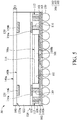
- FIG. 5 is a cross-sectional view of an exemplary semiconductor package structure 50 in accordance with some embodiments of the disclosure. Descriptions of elements of the embodiments hereinafter that are the same as or similar to those previously described with reference to FIG. 1 may be omitted for brevity.
- the semiconductor package structure 50 is similar to the semiconductor package structure 10 shown in FIG. 1 .
- the second antenna element 130b of the antenna 130 in the semiconductor package structure 50 is formed in the molding compound layer 122. More specifically, the second antenna element 130b is formed on the bottom surface 140b of the insulating capping layer 140 with a uniform thickness T3 that may be substantially equal to the thickness T1 shown in FIG. 1 .
- the molding compound layer 122 extends on sidewalls of the second antenna element 130b, so that the second antenna element 130b of the antenna 130 is surrounded by the molding compound layer 122 and separated from the first antenna element 130a of the antenna 130 by the molding compound layer 122.
- the bottom surface and sidewall surfaces of the second antenna element 130b are covered by the molding compound layer 122, and the top surface of the molding compound layer 122 is substantially level with the top surface of the second antenna element 130b of the antenna 130.
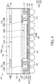
- FIG. 6 is a cross-sectional view of an exemplary semiconductor package structure 60 in accordance with some embodiments of the disclosure. Descriptions of elements of the embodiments hereinafter that are the same as or similar to those previously described with reference to FIGS. 1 , 2 and 5 may be omitted for brevity.
- the semiconductor package structure 60 is similar to the semiconductor package structure 50 shown in FIG. 5 .
- the semiconductor package structure 20 further includes an adhesion layer 124 formed between the molding compound layer 122 and the insulating capping layer 140.
- the second antenna element 130b of the antenna 130 in the semiconductor package structure 60 is formed in the adhesion layer 124.
- the second antenna element 130b is formed on the bottom surface 140b of the insulating capping layer 140.
- the adhesion layer 124 extends on sidewalls of the second antenna element 130b, so that the second antenna element 130b of the antenna 130 is surrounded by the adhesion layer 124.
- the bottom surface and sidewall surfaces of the second antenna element 130b are covered by the adhesion layer 124, and the top surface of the second antenna element 130b is substantially level with the top surface of the adhesion layer 124.
- the insulating capping layer 140 has a uniform thickness T3 that may be substantially equal to the thickness T1 shown in FIG. 1 .
- the adhesion layer 124 has a thickness T4 measured from the top surface 122a of the molding compound layer 122 to the top surface of the adhesion layer 124. In some embodiments, the thickness T4 is in a range from about 10 ⁇ m to about 100 ⁇ m.
- the semiconductor package structure is designed to fabricate an insulating capping/protection layer and antennas integrated into the semiconductor package structure.
- the insulating capping/protection layer prevents the antenna element on the molding compounding layer from being oxidized, delaminated from the underlying molding compounding layer, and/or damaged during testing.
- reliability, yield, and throughput of the semiconductor package structure can be improved.
- reliability, yield, and throughput of the semiconductor package structure are increased and the manufacturing cost of the semiconductor package structure is reduced.
- the integrated capping/protection layer can provide design flexibility for selecting a material of the patch antenna that is integrated in the semiconductor package structure, so as to minimize the antenna loss.
Landscapes
- Engineering & Computer Science (AREA)
- Microelectronics & Electronic Packaging (AREA)
- Structures Or Materials For Encapsulating Or Coating Semiconductor Devices Or Solid State Devices (AREA)
- Physics & Mathematics (AREA)
- Geometry (AREA)
Abstract
Description
- The present invention relates to a semiconductor package structure, and in particular to a fan-out package structure that includes a protected antenna.
- In order to ensure the continued miniaturization and multi-functionality of electronic products and communication devices, semiconductor packages must be small in size, support multi-pin connection, operate at high speeds, and have high functionality. Additionally, in a high-frequency application such as a radio frequency (RF) system-in-package (SiP) assembly, antennas are typically used for enabling wireless communication.
- When wireless communication packages with antennas are constructed, package designs need to provide good antenna properties (such as high efficiency, wide bandwidth, etc) while providing reliable and low cost package solutions. In such a conventional SiP structure, a discrete antenna component is individually encapsulated or mounted on a printed circuit board (PCB) or package. Since the PCB is required to provide additional area for the antenna component mounted thereon, it is difficult to reduce the device size. Additionally, the antenna mounted on the package may induce antenna oxidation, delamination between the antenna and the underlying package, and/or surface damage during testing. As a result, reliability, yield, and throughput of the semiconductor package structure are reduced.
- Thus, a novel semiconductor package structure is desirable.
- Semiconductor package structures are provided. An exemplary embodiment of a semiconductor package structure includes a semiconductor die and a first molding compound layer surrounding the semiconductor die. The semiconductor package structure further includes a first redistribution layer (RDL) structure formed on a non-active surface of the semiconductor die and the first molding compound layer, a second molding compound layer formed on first RDL structure, and an insulating capping layer covering the second molding compound layer. The semiconductor package structure further includes a first antenna electrically coupled to the semiconductor die. The first antenna includes a first antenna element formed in the first RDL structure and a second antenna element formed between the second molding compound layer and the insulating capping layer.
- The semiconductor package structure may further comprise a second RDL structure formed on and electrically coupled to an active surface of the semiconductor die; a second antenna formed in the first molding compound layer and electrically coupled to the semiconductor die via the second RDL structure; and a through via structure formed in the first molding compound layer and electrically coupled between the first antenna element and the second RDL structure, so that the semiconductor die is electrically coupled to the first antenna.
- The first antenna may be a patch antenna and the second antenna may be a dipole antenna.
- The semiconductor package structure may further comprise a plurality of conductive structures electrically coupled to the semiconductor die via the second RDL structure.
- The semiconductor package structure may further comprise an adhesion layer formed between the second molding compound layer and the insulating capping layer.
- The adhesion layer may extend on sidewalls of the second antenna element, so that the second antenna element is surrounded by the adhesion layer.
- The insulating capping layer and the adhesion layer may be respectively formed of a material selected from polyimide, silicon nitride, silicon oxynitride, or Ajinomoto™ Build-up Film (ABF).
- The insulating capping layer may be formed of a material that is different from that of the adhesion layer.
- The second molding compound layer may extend on sidewalls of the second antenna element, so that the second antenna element is surrounded by the second molding compound layer.
- The insulating capping layer may have a substantially flat top surface.
- The insulating capping layer may have a substantially uniform thickness, and a top surface and sidewall surfaces of the second antenna element may be conformally covered by the insulating capping layer.
- Another exemplary embodiment of a semiconductor package structure includes a semiconductor die and a first molding compound layer surrounding the semiconductor die. The semiconductor package structure further includes a second molding compound layer formed above a first side of the semiconductor die and the first molding compound layer, a through via structure formed in the first molding compound layer, and an insulating capping layer covering the second molding compound layer. The semiconductor package structure further includes a patch antenna and a dipole antenna. The patch antenna includes a first antenna element formed between the first molding compound layer and the second molding compound layer and electrically coupled to the semiconductor die by the through via structure, and a second antenna element having a top surface and sidewall surfaces covered by the insulating capping layer. The dipole antenna is formed in the first molding compound layer.
- The semiconductor package structure may further comprise a redistribution layer (RDL) structure separating the semiconductor die from the second molding compound layer, wherein the first antenna element is in the RDL structure.
- The semiconductor package structure may further comprise an RDL structure formed on a second side of the semiconductor die opposite the first side; and a plurality of conductive structures electrically coupled to the semiconductor die via the RDL structure. The semiconductor die may be electrically coupled to the through via structure by the RDL structure.
- The semiconductor package structure may further comprise an adhesion layer between the second molding compound layer and the second antenna element.
- The insulating capping layer and the adhesion layer may be formed of different materials.
- The insulating capping layer may have a substantially flat top surface.
- The insulating capping layer may have a substantially uniform thickness, so that the top and the sidewalls of the second antenna element are conformally covered by the insulating capping layer.
- Yet another exemplary embodiment of a semiconductor package structure includes a semiconductor die and a first molding compound layer surrounding the semiconductor die. The semiconductor package structure further includes a second molding compound layer formed above the semiconductor die and the first molding compound layer, a through via structure formed in the first molding compound layer, and an insulating capping layer covering the second molding compound layer. The semiconductor package structure further includes a patch antenna and a dipole antenna. The patch antenna includes a first antenna element formed between the first molding compound layer and the second molding compound layer and electrically coupled to the semiconductor die via the through via structure, and a second antenna element formed on a bottom surface of the insulating capping layer and separated from the first antenna element by the second molding compound layer. The dipole antenna formed in the first molding compound layer.
- The semiconductor package structure may further comprise a redistribution layer (RDL) structure separating the semiconductor die from the second molding compound layer, wherein the first antenna element is in the RDL structure.
- The semiconductor package structure may further comprise a plurality of conductive structures formed below the semiconductor die; and an RDL structure electrically coupled between the semiconductor die via and the plurality of conductive structures. The semiconductor die may be electrically coupled to the through via structure by the RDL structure.
- The semiconductor package structure may further comprise an adhesion layer between the second molding compound layer and the insulating capping layer.
- A bottom surface and sidewall surfaces of the second antenna element may be covered by the adhesion layer. A top surface of the second antenna element may be substantially level with a top surface of the adhesion layer.
- The insulating capping layer may have a substantially flat top surface.
- A bottom surface and sidewall surfaces of the second antenna element may be covered by the second molding compound layer. A top surface of the second antenna element may be substantially level with a top surface of the second molding compound layer.
- The insulating capping layer and the adhesion layer may be formed of different materials.
- A detailed description is given in the following embodiments with reference to the accompanying drawings.
- The present invention can be more fully understood by reading the subsequent detailed description and examples with references made to the accompanying drawings, wherein:
-
FIG. 1 is a cross-sectional view of an exemplary semiconductor package structure in accordance with some embodiments. -
FIG. 2 is a cross-sectional view of an exemplary semiconductor package structure in accordance with some embodiments. -
FIG. 3 is a cross-sectional view of an exemplary semiconductor package structure in accordance with some embodiments. -
FIG. 4 is a cross-sectional view of an exemplary semiconductor package structure in accordance with some embodiments. -
FIG. 5 is a cross-sectional view of an exemplary semiconductor package structure in accordance with some embodiments. -
FIG. 6 is a cross-sectional view of an exemplary semiconductor package structure in accordance with some embodiments. - The following description is of the best-contemplated mode of carrying out the invention. This description is made for the purpose of illustrating the general principles of the invention and should not be taken in a limiting sense. The scope of the invention is determined by reference to the appended claims.
- The present invention will be described with respect to particular embodiments and with reference to certain drawings, but the invention is not limited thereto and is only limited by the claims. The drawings described are only schematic and are non-limiting. In the drawings, the size of some of the elements may be exaggerated for illustrative purposes and not drawn to scale. The dimensions and the relative dimensions do not correspond to actual dimensions in the practice of the invention.
-
FIG. 1 is a cross-sectional view of an exemplarysemiconductor package structure 10 in accordance with some embodiments. In some embodiments, thesemiconductor package structure 10 is a wafer-level semiconductor package structure, and is a flip-chip semiconductor package structure. As shown inFIG. 1 , thesemiconductor package structure 10 is mounted on a base (not shown), in accordance with some embodiments. For example, the semiconductor package structure may be a system-on-chip (SOC) package structure. Moreover, the base may include a printed circuit board (PCB) and may be formed of polypropylene (PP). Alternatively, the base is a package substrate. Thesemiconductor package structure 10 is mounted onto the base by a bonding process. For example, thesemiconductor package structure 10 includesconductive structures 150 that is mounted on and electrically coupled to the base by the bonding process. In some embodiments, each of theconductive structures 150 includes a conductive bump structure such as a copper bump or a solder bump structure, as shown inFIG. 1 . Alternatively, each of theconductive structures 150 includes a conductive pillar structure, a conductive wire structure, or a conductive paste structure. - In some embodiments, the
semiconductor package structure 10 further includes asemiconductor die 100, such as a system-on-chip (SOC) die. For example, the SOC die may includes a microcontroller (MCU), a microprocessor (MPU), a power management integrated circuit (PMIC), a global positioning system (GPS) device, or a radio frequency (RF) device or any combination thereof. - In some embodiments, the semiconductor die 100 has two opposing sides. More specifically, the semiconductor die 100 has a
non-active surface 100a (which is also referred to as a rear surface) and anactive surface 100b (which is also referred to as a front surface) opposite thenon-active surface 100a.Pads 101 of the semiconductor die 100 are disposed on theactive surface 100b and electrically connected to the circuitry (not shown) of the semiconductor die 100. In some embodiments, thepads 101 of the semiconductor die 100 belong to the uppermost metal layer of the interconnection structure (not shown) of the semiconductor die 100. It should be noted that the number of semiconductor dies integrated in thesemiconductor package structure 10 is not limited to that disclosed in the embodiment. - In some embodiments, the
semiconductor package structure 10 further includes amolding compound layer 108 surrounds the semiconductor die 100. In some embodiments, themolding compound layer 108 may be formed of an epoxy, a resin, a moldable polymer, or the like. Themolding compound layer 108 may be applied while substantially liquid, and then may be cured through a chemical reaction, such as in an epoxy or resin. In some other embodiments, themolding compound layer 108 may be an ultraviolet (UV) or thermally cured polymer applied as a gel or malleable solid capable of being disposed around the semiconductor die 100, and then may be cured through a UV or thermal curing process. Themolding compound layer 108 may be cured with a mold (not shown). - In some embodiments, the
semiconductor package structure 10 further includes a redistribution layer (RDL)structure 106 formed below the semiconductor die 100 and themolding compound layer 108. TheRDL structure 106, which is also referred to as a fan-out structure. TheRDL structure 106 is disposed on theactive surface 100b of the semiconductor die 100 and electrically connected thereto through thepads 101. Moreover, theconductive structures 150 are mounted on and electrically coupled to theRDL structure 106, such that theconductive structures 150 are separated from themolding compound layer 108 and the semiconductor die 100 through theRDL structure 106. In other words, theconductive structures 150 are free from contact with themolding compound layer 108 and the semiconductor die 100. - In some embodiments, the
RDL structure 106 includes one or more conductive traces disposed in an inter-metal dielectric (IMD)layer 102. Conductive traces 103 are disposed at a first layer-level of theIMD layer 102 and at least one of the conductive traces 103 is electrically coupled to the semiconductor die 100. Moreover,conductive traces 105 are disposed at a second layer-level that is different from the first layer-level of theIMD layer 102. Moreover, at least one of the conductive traces 105 is electrically coupled to one or moreconductive structures 150, so that theconductive structures 150 are electrically coupled to the semiconductor die 100 via theRDL structure 106. - In some embodiments, the
IMD layer 102 includes a firstsub-dielectric layer 102a and a secondsub-dielectric layer 102b successively stacked from theactive surface 100b of the semiconductor die 100, such that theconductive traces 103 are formed in the firstsub-dielectric layer 102a, and theconductive traces 105 are formed in the secondsub-dielectric layer 102b. It should be noted that the number of conductive traces and the number of sub-dielectric layers of theRDL structure 106 shown inFIG. 1 are only an example and are not a limitation to the present invention. - In some embodiments, the
IMD layer 102 is formed of an organic material, which includes a polymer base material, a non-organic material, which includes silicon nitride (SiNX), silicon oxide (SiOX), graphene, or the like. For example, the firstsub-dielectric layers 102a and the secondsub-dielectric layer 102b are made of a polymer base material. In some other embodiments, theIMD layer 102 is a high-k dielectric layer (k is the dielectric constant of the dielectric layer). In some other embodiments, theIMD layer 102 may be formed of a photo sensitive material, which includes a dry film photoresist, or a taping film. - In some embodiments, the
semiconductor package structure 10 further includes one or more through viastructures 110 formed in and passing through themolding compound layer 108. The through viastructures 110 are electrically coupled to theconductive traces 103 of theRDL structure 106. The through viastructures 110 may be referred to as through insulator vias (TIVs) and be formed of copper. - In some embodiments, the
semiconductor package structure 10 further includes anRDL structure 120 formed above the semiconductor die 100 and themolding compound layer 108. TheRDL structure 120 may have a structure similar to theRDL structure 106 and is also referred to as a fan-out structure. In some embodiments, thenon-active surface 100a of the semiconductor die 100 is adhered to theRDL structure 120 via anadhesion layer 114, such that the semiconductor die 100 and themolding compound layer 108 are interposed between theRDL structure 106 and theRDL structure 120. - In some embodiments, the
RDL structure 120 is disposed on themolding compound layer 108 and the semiconductor die 100 and includes anIMD layer 121 and conductive traces (not shown) in theIMD layer 121. TheIMD layer 121 may be a single layer or a multi-layer structure. The method and material used for forming theIMD layer 121 may be the same as or similar to those of theIMD layer 102. Similarly, the method and material used for forming the conductive traces of theRDL structure 120 may be the same as or similar to those of theconductive traces RDL structure 106. In other words, the process for forming theRDL structure 106 can be used for forming theRDL structure 120. - In some embodiments, the
semiconductor package structure 10 further includes amolding compound layer 122 formed on theRDL structure 120 above thenon-active surface 100a of the semiconductor die 100 and themolding compound layer 108. Therefore, theRDL structure 120 separates the semiconductor die 100 from themolding compound layer 122. In some embodiments, the method and material used for forming themolding compound layer 122 may be the same as or similar to those of themolding compound layer 108. - In some embodiments, the
semiconductor package structure 10 further includes one ormore antennas 112 and one ormore antennas 130 therein and electrically coupled to the semiconductor die 100. More specifically, in some embodiments, theantenna 112 is formed in themolding compound layer 108, and the through viastructure 110 in themolding compound layer 108 is disposed between the semiconductor die 100 and theantenna 112. Theantenna 112 is electrically coupled to the semiconductor die 100 via at least one of theconductive traces 103 of theRDL structure 106. In some embodiments, theantenna 112 is a dipole antenna. In some embodiments, the methods and materials used for forming theantenna 112 may be the same as or similar to those of the through viastructure 110. - In some embodiments, unlike the
antenna 112, theantenna 130 includes afirst antenna element 130a and asecond antenna element 130b that is separated from thefirst antenna element 130a. More specifically, in some embodiments, thefirst antenna element 130a is embedded in theIMD layer 121 of theRDL structure 120, so that thefirst antenna element 130a is formed between themolding compound layer 108 and themolding compound layer 122. Thesecond antenna element 130b is formed on and in direct contact with themolding compound layer 122, so that thefirst antenna element 130a is separated from thesecond antenna element 130b by themolding compound layer 122. In some embodiments, the through viastructure 110 formed in themolding compound layer 108 is electrically coupled between thefirst antenna element 130a and at least one of theconductive traces 103 of theRDL structure 106, so that the semiconductor die 100 is electrically coupled to theantenna 130. In some embodiments, theantenna 130 is a patch antenna using themolding compound layer 122 as a resonator. Therefore, the thickness of themolding compound layer 122 depends on the desired dielectric constant (Dk) and the desired dissipation factor (Df, which is also referred to as loss tangent) for theantenna 130. In some embodiments, thefirst antenna element 130a is formed of at least one of the conductive traces in theRDL structure 120. In those cases, the methods and materials used for forming thefirst antenna element 130a may be the same as or similar to those of theconductive traces IMD layer 102 of theRDL structure 106. - In some embodiments, the
semiconductor package structure 10 further includes an insulatingcapping layer 140 covering and in direct contact with thetop surface 122a of themolding compound layer 122 and the top surface and the sidewall surfaces of thesecond antenna element 130b, so that thesecond antenna element 130b is formed between themolding compound layer 122 and the insulatingcapping layer 140. - In some embodiments, the insulating
capping layer 140 serves as a protection layer for preventing thesecond antenna element 130b of theantenna 130 from being oxidized or damaged. The insulatingcapping layer 140 has a substantially flattop surface 140a and has a thickness T1 measured from thetop surface 122a of themolding compound layer 122 to thetop surface 140a. In some embodiments, the thickness T1 is in a range from about 10µm to about 100µm. In some embodiments, the insulatingcapping layer 140 is made of polyimide, silicon nitride, silicon oxynitride, Ajinomoto™ Build-up Film (ABF), or other suitable organic materials. In some embodiments, the insulatingcapping layer 140 is formed by a lamination process. -
FIG. 2 is a cross-sectional view of an exemplarysemiconductor package structure 20 in accordance with some embodiments of the disclosure. Descriptions of elements of the embodiments hereinafter that are the same as or similar to those previously described with reference toFIG. 1 may be omitted for brevity. In the embodiment, thesemiconductor package structure 20 is similar to thesemiconductor package structure 10 shown inFIG. 1 , except that thesemiconductor package structure 20 further includes anadhesion layer 124 formed between themolding compound layer 122 and the insulatingcapping layer 140. Theadhesion layer 124 between themolding compound layer 122 and thesecond antenna element 130b of theantenna 130 can improve the adhesion therebetween. - In some embodiments, the
adhesion layer 124 is formed of a material selected from polyimide, silicon nitride, silicon oxynitride, or ABF. In some embodiments, theadhesion layer 124 is formed of a material that is different from that of the insulatingcapping layer 140. -
FIG. 3 is a cross-sectional view of an exemplarysemiconductor package structure 30 in accordance with some embodiments of the disclosure. Descriptions of elements of the embodiments hereinafter that are the same as or similar to those previously described with reference toFIG. 1 may be omitted for brevity. In the embodiment, thesemiconductor package structure 30 is similar to thesemiconductor package structure 10 shown inFIG. 1 . Unlike the insulatingcapping layer 140 in thesemiconductor package structure 10, the insulating capping layer 140' in thesemiconductor package structure 30 has a substantially uniform thickness T2, and the top surface and sidewall surfaces of thesecond antenna element 130b of theantenna 130 is conformally covered by the insulating capping layer 140'. - In some embodiments, the insulating capping layer 140' has a thickness measured from the
top surface 122a of themolding compound layer 122 to thetop surface 141 of a portion of the insulating capping layer 140' that is in direct to themolding compound layer 122. In some embodiments, such a thickness may be substantially equal to the thickness T2. In some embodiments, the insulating capping layer 140' has a height H measured from thetop surface 122a of themolding compound layer 122 to thetop surface 143 of a portion of the insulating capping layer 140' above thesecond antenna element 130b of theantenna 130. In some embodiments, the height H is in a range from about 10µm to about 100µm. In some embodiments, the insulating capping layer 140' is formed by a deposition process (such as chemical vapor deposition (CVD)) or a coating process. -
FIG. 4 is a cross-sectional view of an exemplarysemiconductor package structure 40 in accordance with some embodiments of the disclosure. Descriptions of elements of the embodiments hereinafter that are the same as or similar to those previously described with reference toFIGS. 1 ,2 and3 and may be omitted for brevity. In the embodiment, thesemiconductor package structure 40 is similar to thesemiconductor package structure 30 shown inFIG. 3 , except that the semiconductor package of thesemiconductor package structure 40 further includes anadhesion layer 124 formed between themolding compound layer 122 and the insulatingcapping layer 140. Theadhesion layer 124 between themolding compound layer 122 and thesecond antenna element 130b of theantenna 130 can improve the adhesion therebetween. -
FIG. 5 is a cross-sectional view of an exemplarysemiconductor package structure 50 in accordance with some embodiments of the disclosure. Descriptions of elements of the embodiments hereinafter that are the same as or similar to those previously described with reference toFIG. 1 may be omitted for brevity. In the embodiment, thesemiconductor package structure 50 is similar to thesemiconductor package structure 10 shown inFIG. 1 . Unlike thesemiconductor package structure 10, thesecond antenna element 130b of theantenna 130 in thesemiconductor package structure 50 is formed in themolding compound layer 122. More specifically, thesecond antenna element 130b is formed on thebottom surface 140b of the insulatingcapping layer 140 with a uniform thickness T3 that may be substantially equal to the thickness T1 shown inFIG. 1 . - Moreover, the
molding compound layer 122 extends on sidewalls of thesecond antenna element 130b, so that thesecond antenna element 130b of theantenna 130 is surrounded by themolding compound layer 122 and separated from thefirst antenna element 130a of theantenna 130 by themolding compound layer 122. In this case, the bottom surface and sidewall surfaces of thesecond antenna element 130b are covered by themolding compound layer 122, and the top surface of themolding compound layer 122 is substantially level with the top surface of thesecond antenna element 130b of theantenna 130. -
FIG. 6 is a cross-sectional view of an exemplarysemiconductor package structure 60 in accordance with some embodiments of the disclosure. Descriptions of elements of the embodiments hereinafter that are the same as or similar to those previously described with reference toFIGS. 1 ,2 and5 may be omitted for brevity. In the embodiment, thesemiconductor package structure 60 is similar to thesemiconductor package structure 50 shown inFIG. 5 . Unlike thesemiconductor package structure 50, thesemiconductor package structure 20 further includes anadhesion layer 124 formed between themolding compound layer 122 and the insulatingcapping layer 140. Moreover, thesecond antenna element 130b of theantenna 130 in thesemiconductor package structure 60 is formed in theadhesion layer 124. - More specifically, the
second antenna element 130b is formed on thebottom surface 140b of the insulatingcapping layer 140. Moreover, theadhesion layer 124 extends on sidewalls of thesecond antenna element 130b, so that thesecond antenna element 130b of theantenna 130 is surrounded by theadhesion layer 124. In this case, the bottom surface and sidewall surfaces of thesecond antenna element 130b are covered by theadhesion layer 124, and the top surface of thesecond antenna element 130b is substantially level with the top surface of theadhesion layer 124. - In some embodiments, the insulating
capping layer 140 has a uniform thickness T3 that may be substantially equal to the thickness T1 shown inFIG. 1 . In some embodiments, theadhesion layer 124 has a thickness T4 measured from thetop surface 122a of themolding compound layer 122 to the top surface of theadhesion layer 124. In some embodiments, the thickness T4 is in a range from about 10µm to about 100µm. - According to the foregoing embodiments, the semiconductor package structure is designed to fabricate an insulating capping/protection layer and antennas integrated into the semiconductor package structure. The insulating capping/protection layer prevents the antenna element on the molding compounding layer from being oxidized, delaminated from the underlying molding compounding layer, and/or damaged during testing. As a result, reliability, yield, and throughput of the semiconductor package structure can be improved. As a result, reliability, yield, and throughput of the semiconductor package structure are increased and the manufacturing cost of the semiconductor package structure is reduced. Additionally, the integrated capping/protection layer can provide design flexibility for selecting a material of the patch antenna that is integrated in the semiconductor package structure, so as to minimize the antenna loss.
- While the invention has been described by way of example and in terms of the preferred embodiments, it is to be understood that the invention is not limited to the disclosed embodiments. On the contrary, it is intended to cover various modifications and similar arrangements (as would be apparent to those skilled in the art). Therefore, the scope of the appended claims should be accorded the broadest interpretation so as to encompass all such modifications and similar arrangements.
Claims (11)
- A semiconductor package structure, comprising:a semiconductor die;a first molding compound layer surrounding the semiconductor die;a first redistribution layer (RDL) structure formed on a non-active surface of the semiconductor die and the first molding compound layer;a second molding compound layer formed on first RDL structure;an insulating capping layer covering the second molding compound layer; anda first antenna electrically coupled to the semiconductor die, comprising:a first antenna element formed in the first RDL structure; anda second antenna element formed between the second molding compound layer and the insulating capping layer.
- The semiconductor package structure as claimed in claim 1, further comprising:a second RDL structure formed on and electrically coupled to an active surface of the semiconductor die;a second antenna formed in the first molding compound layer and electrically coupled to the semiconductor die via the second RDL structure;a through via structure formed in the first molding compound layer and electrically coupled between the first antenna element and the second RDL structure, so that the semiconductor die is electrically coupled to the first antenna.
- The semiconductor package structure as claimed in claim 2, wherein the first antenna is a patch antenna and the second antenna is a dipole antenna.
- The semiconductor package structure as claimed in claim 2 or 3, further comprising a plurality of conductive structures electrically coupled to the semiconductor die via the second RDL structure.
- The semiconductor package structure as claimed in any preceding claim, further comprising an adhesion layer formed between the second molding compound layer and the insulating capping layer.
- The semiconductor package structure as claimed in claim 5, wherein the adhesion layer extends on sidewalls of the second antenna element, so that the second antenna element is surrounded by the adhesion layer.
- The semiconductor package structure as claimed in claim 5 or 6, wherein the insulating capping layer and the adhesion layer are respectively formed of a material selected from polyimide, silicon nitride, silicon oxynitride, or Ajinomoto™ Build-up Film (ABF).
- The semiconductor package structure as claimed in any of claims 5-7, wherein the insulating capping layer is formed of a material that is different from that of the adhesion layer.
- The semiconductor package structure as claimed in any preceding claim, wherein the second molding compound layer extends on sidewalls of the second antenna element, so that the second antenna element is surrounded by the second molding compound layer.
- The semiconductor package structure as claimed in any preceding claim, wherein the insulating capping layer has a substantially flat top surface.
- The semiconductor package structure as claimed in any preceding claim, wherein the insulating capping layer has a substantially uniform thickness, and wherein a top surface and sidewall surfaces of the second antenna element is conformally covered by the insulating capping layer.
Applications Claiming Priority (2)
| Application Number | Priority Date | Filing Date | Title |
|---|---|---|---|
| US201862670920P | 2018-05-14 | 2018-05-14 | |
| US16/387,354 US11043730B2 (en) | 2018-05-14 | 2019-04-17 | Fan-out package structure with integrated antenna |
Publications (1)
| Publication Number | Publication Date |
|---|---|
| EP3570323A1 true EP3570323A1 (en) | 2019-11-20 |
Family
ID=66476384
Family Applications (1)
| Application Number | Title | Priority Date | Filing Date |
|---|---|---|---|
| EP19173046.4A Pending EP3570323A1 (en) | 2018-05-14 | 2019-05-07 | Fan-out package structure with integrated antenna |
Country Status (4)
| Country | Link |
|---|---|
| US (2) | US11043730B2 (en) |
| EP (1) | EP3570323A1 (en) |
| CN (2) | CN114864559A (en) |
| TW (1) | TW201947728A (en) |
Cited By (1)
| Publication number | Priority date | Publication date | Assignee | Title |
|---|---|---|---|---|
| EP4071928A4 (en) * | 2020-02-25 | 2023-01-25 | Honor Device Co., Ltd. | ANTENNA CONNECTION APPARATUS, ANTENNA ASSEMBLY AND ELECTRONIC DEVICE |
Families Citing this family (22)
| Publication number | Priority date | Publication date | Assignee | Title |
|---|---|---|---|---|
| US11043730B2 (en) | 2018-05-14 | 2021-06-22 | Mediatek Inc. | Fan-out package structure with integrated antenna |
| US11024954B2 (en) | 2018-05-14 | 2021-06-01 | Mediatek Inc. | Semiconductor package with antenna and fabrication method thereof |
| US20190348747A1 (en) * | 2018-05-14 | 2019-11-14 | Mediatek Inc. | Innovative air gap for antenna fan out package |
| US10748861B2 (en) * | 2018-05-16 | 2020-08-18 | Taiwan Semiconductor Manufacturing Co., Ltd. | Package structure and manufacturing method thereof |
| US11081453B2 (en) | 2018-07-03 | 2021-08-03 | Mediatek Inc. | Semiconductor package structure with antenna |
| US10840197B2 (en) * | 2018-10-30 | 2020-11-17 | Taiwan Semiconductor Manufacturing Company, Ltd. | Package structure and manufacturing method thereof |
| KR102561724B1 (en) * | 2018-12-07 | 2023-07-31 | 삼성전자주식회사 | Antenna Module and the Electronic Device including the Antenna Module |
| DE102019124237A1 (en) * | 2018-12-28 | 2020-07-02 | Taiwan Semiconductor Manufacturing Co., Ltd. | HETEROGENEOUS ANTENNA IN FAN OUT PACKAGE |
| US11532867B2 (en) * | 2018-12-28 | 2022-12-20 | Taiwan Semiconductor Manufacturing Company, Ltd. | Heterogeneous antenna in fan-out package |
| CN110943054A (en) * | 2019-12-06 | 2020-03-31 | 上海先方半导体有限公司 | A kind of multi-channel AiP packaging structure and preparation method thereof |
| KR102731798B1 (en) | 2019-12-10 | 2024-11-19 | 삼성전기주식회사 | Antenna substrate and antenna module comprising the same |
| CN111128909A (en) * | 2019-12-10 | 2020-05-08 | 中国电子科技集团公司第五十八研究所 | Radio frequency system micro packaging structure and preparation method thereof |
| TWI711131B (en) * | 2019-12-31 | 2020-11-21 | 力成科技股份有限公司 | Chip package structure |
| US11205627B2 (en) * | 2020-02-12 | 2021-12-21 | Advanced Semiconductor Engineering, Inc. | Semiconductor device package including emitting devices and method of manufacturing the same |
| KR102762869B1 (en) * | 2020-04-14 | 2025-02-07 | 삼성전기주식회사 | Antenna |
| US12212064B2 (en) * | 2020-10-27 | 2025-01-28 | Mixcomm, Inc. | Methods and apparatus for implementing antenna assemblies and/or combining antenna assemblies to form arrays |
| TWI774221B (en) * | 2021-01-29 | 2022-08-11 | 隆達電子股份有限公司 | Light-emitting device and method for manufacturing the same |
| TWI778654B (en) * | 2021-06-09 | 2022-09-21 | 矽品精密工業股份有限公司 | Electronic package and manufacturing method thereof |
| US20230078536A1 (en) * | 2021-09-14 | 2023-03-16 | Apple Inc. | Conductive features on system-in-package surfaces |
| US12212082B2 (en) * | 2022-09-23 | 2025-01-28 | Qualcomm Incorporated | Antenna system with floating conductor |
| CN116888734A (en) * | 2022-10-24 | 2023-10-13 | 广东省科学院半导体研究所 | Fan-out packaging structure and preparation method thereof |
| TWI859849B (en) * | 2023-05-10 | 2024-10-21 | 矽品精密工業股份有限公司 | Electronic package and manufacturing method thereof |
Citations (5)
| Publication number | Priority date | Publication date | Assignee | Title |
|---|---|---|---|---|
| US20070029667A1 (en) * | 2005-08-05 | 2007-02-08 | Shinko Electric Industries Co., Ltd. | Semiconductor device |
| EP3091571A2 (en) * | 2015-05-05 | 2016-11-09 | MediaTek, Inc | Fan-out package structure including an antenna or a conductive shielding layer |
| US20180166405A1 (en) * | 2016-12-13 | 2018-06-14 | Taiwan Semiconductor Manufacturing Co. Ltd. | Structure and formation method of chip package with antenna element |
| EP3413347A1 (en) * | 2017-06-07 | 2018-12-12 | MediaTek Inc. | Semiconductor package having discrete antenna device |
| US20190096828A1 (en) * | 2017-09-28 | 2019-03-28 | Taiwan Semiconductor Manufacturing Co., Ltd., Hsinchu, TAIWAN | Semiconductor package structure |
Family Cites Families (52)
| Publication number | Priority date | Publication date | Assignee | Title |
|---|---|---|---|---|
| JP4409014B2 (en) | 1999-11-30 | 2010-02-03 | リンテック株式会社 | Manufacturing method of semiconductor device |
| JP2006108654A (en) * | 2004-09-09 | 2006-04-20 | Semiconductor Energy Lab Co Ltd | Wireless chip |
| EP1797617A4 (en) * | 2004-10-01 | 2009-08-12 | Rochemont L Pierre De | CERAMIC ANTENNA MODULE AND METHODS OF MAKING SAME |
| JP2008545274A (en) | 2005-06-30 | 2008-12-11 | フェアチャイルド セミコンダクター コーポレイション | Semiconductor die package and manufacturing method thereof |
| KR20090006336A (en) * | 2007-07-11 | 2009-01-15 | 삼성전기주식회사 | Case integrated antenna and manufacturing method |
| KR101075192B1 (en) | 2009-03-03 | 2011-10-21 | 도레이첨단소재 주식회사 | Adhesive tape for manufacturing electronic component |
| KR101705742B1 (en) * | 2009-11-20 | 2017-02-10 | 히타치 긴조쿠 가부시키가이샤 | Antenna |
| US8407890B2 (en) * | 2010-01-25 | 2013-04-02 | Freescale Semiconductor Inc. | Method of manufacting an electronic device module with integrated antenna structure |
| US9007273B2 (en) * | 2010-09-09 | 2015-04-14 | Advances Semiconductor Engineering, Inc. | Semiconductor package integrated with conformal shield and antenna |
| US8816906B2 (en) * | 2011-05-05 | 2014-08-26 | Intel Corporation | Chip packages including through-silicon via dice with vertically inegrated phased-array antennas and low-frequency and power delivery substrates |
| US9711465B2 (en) | 2012-05-29 | 2017-07-18 | Taiwan Semiconductor Manufacturing Co., Ltd. | Antenna cavity structure for integrated patch antenna in integrated fan-out packaging |
| US9153542B2 (en) | 2012-08-01 | 2015-10-06 | Advanced Semiconductor Engineering, Inc. | Semiconductor package having an antenna and manufacturing method thereof |
| US8866292B2 (en) * | 2012-10-19 | 2014-10-21 | Infineon Technologies Ag | Semiconductor packages with integrated antenna and methods of forming thereof |
| US9431369B2 (en) * | 2012-12-13 | 2016-08-30 | Taiwan Semiconductor Manufacturing Company, Ltd. | Antenna apparatus and method |
| US8890284B2 (en) | 2013-02-22 | 2014-11-18 | Infineon Technologies Ag | Semiconductor device |
| EP3080841A4 (en) | 2013-12-09 | 2017-08-23 | Intel Corporation | Antenna on ceramics for a packaged die |
| CN106165196A (en) | 2014-04-18 | 2016-11-23 | 川斯普公司 | Metamaterial substrate for circuit design |
| US9472859B2 (en) | 2014-05-20 | 2016-10-18 | International Business Machines Corporation | Integration of area efficient antennas for phased array or wafer scale array antenna applications |
| US9843106B2 (en) | 2014-10-09 | 2017-12-12 | Taiwan Semicondcutor Manufacturing Company, Ltd. | Integrated fan out antenna and method of forming the same |
| US10636753B2 (en) * | 2015-07-29 | 2020-04-28 | STATS ChipPAC Pte. Ltd. | Antenna in embedded wafer-level ball-grid array package |
| US9953936B2 (en) * | 2015-10-30 | 2018-04-24 | Taiwan Semiconductor Manufacturing Company Ltd. | Semiconductor structure and manufacturing method thereof |
| US9741693B2 (en) | 2015-11-12 | 2017-08-22 | Taiwan Semiconductor Manufacturing Company Ltd. | Semiconductor package and method of forming the same |
| EP3360083B1 (en) * | 2015-11-12 | 2023-10-25 | DeepMind Technologies Limited | Dueling deep neural networks |
| CA3018260A1 (en) | 2016-03-24 | 2017-09-28 | Koninklijke Philips N.V. | Method and apparatus for monitoring urination of a subject |
| US10157807B2 (en) * | 2016-05-26 | 2018-12-18 | Taiwan Semiconductor Manufacturing Co., Ltd. | Sensor packages and manufacturing mehtods thereof |
| US10770795B2 (en) | 2016-05-27 | 2020-09-08 | Taiwan Semiconductor Manufacturing Co., Ltd. | Antenna device and method for manufacturing antenna device |
| US10032722B2 (en) | 2016-05-31 | 2018-07-24 | Taiwan Semiconductor Manufacturing Co., Ltd. | Semiconductor package structure having am antenna pattern and manufacturing method thereof |
| EP3479401A4 (en) | 2016-07-01 | 2020-03-04 | INTEL Corporation | SEMICONDUCTOR PACKAGES WITH ANTENNAS |
| US10269732B2 (en) | 2016-07-20 | 2019-04-23 | Taiwan Semiconductor Manufacturing Company, Ltd. | Info package with integrated antennas or inductors |
| US10186756B2 (en) | 2016-08-01 | 2019-01-22 | Intel IP Corporation | Antennas in electronic devices |
| US10224298B2 (en) | 2016-09-02 | 2019-03-05 | Advanced Semiconductor Engineering, Inc. | Semiconductor package device having glass transition temperature greater than binding layer temperature |
| US9935065B1 (en) | 2016-12-21 | 2018-04-03 | Infineon Technologies Ag | Radio frequency device packages and methods of formation thereof |
| US10354964B2 (en) | 2017-02-24 | 2019-07-16 | Taiwan Semiconductor Manufacturing Company, Ltd. | Integrated devices in semiconductor packages and methods of forming same |
| US10460987B2 (en) * | 2017-05-09 | 2019-10-29 | Taiwan Semiconductor Manufacturing Company Ltd. | Semiconductor package device with integrated antenna and manufacturing method thereof |
| US10312112B2 (en) | 2017-06-20 | 2019-06-04 | Taiwan Semiconductor Manufacturing Co., Ltd. | Integrated fan-out package having multi-band antenna and method of forming the same |
| US10186492B1 (en) | 2017-07-18 | 2019-01-22 | Taiwan Semiconductor Manufacturing Co., Ltd. | Package structure and manufacturing method thereof |
| US10461034B2 (en) | 2017-07-26 | 2019-10-29 | Taiwan Semiconductor Manufacturing Co., Ltd. | Package structure and manufacturing method thereof |
| US10685924B2 (en) * | 2017-08-24 | 2020-06-16 | Qualcomm Incorporated | Antenna-on-package arrangements |
| US10157834B1 (en) * | 2017-09-18 | 2018-12-18 | Taiwan Semiconductor Manufacturing Co., Ltd. | Electronic apparatus |
| US10867938B2 (en) | 2017-09-25 | 2020-12-15 | Taiwan Semiconductor Manufacturing Company, Ltd. | Package structure |
| US10276920B2 (en) * | 2017-09-28 | 2019-04-30 | Taiwan Semiconductor Manufacturing Co., Ltd. | Package structure, electronic device and method of fabricating package structure |
| US10483617B2 (en) * | 2017-09-29 | 2019-11-19 | Taiwan Semiconductor Manufacturing Co., Ltd. | Package structure |
| DE112017007887T5 (en) * | 2017-09-29 | 2020-05-07 | Intel Corporation | ANTENNA PACKAGE WITH BALL MOUNT ARRAY TO CONNECT ANTENNA AND BASE SUBSTRATES |
| US10629539B2 (en) * | 2017-11-07 | 2020-04-21 | Taiwan Semiconductor Manufacturing Co., Ltd. | Package structure and method of fabricating the same |
| EP3486943A1 (en) * | 2017-11-17 | 2019-05-22 | MediaTek Inc | Semiconductor package |
| US10325786B1 (en) * | 2017-12-07 | 2019-06-18 | Sj Semiconductor (Jiangyin) Corporation | Double-sided plastic fan-out package structure having antenna and manufacturing method thereof |
| US10468355B2 (en) | 2017-12-08 | 2019-11-05 | Taiwan Semiconductor Manufacturing Company, Ltd. | EMI Shielding structure in InFO package |
| US10424550B2 (en) * | 2017-12-19 | 2019-09-24 | National Chung Shan Institute Of Science And Technology | Multi-band antenna package structure, manufacturing method thereof and communication device |
| US11043730B2 (en) | 2018-05-14 | 2021-06-22 | Mediatek Inc. | Fan-out package structure with integrated antenna |
| US11024954B2 (en) | 2018-05-14 | 2021-06-01 | Mediatek Inc. | Semiconductor package with antenna and fabrication method thereof |
| US20190348747A1 (en) | 2018-05-14 | 2019-11-14 | Mediatek Inc. | Innovative air gap for antenna fan out package |
| US10868353B2 (en) * | 2018-09-27 | 2020-12-15 | Taiwan Semiconductor Manufacturing Company, Ltd. | Electronic device and manufacturing method thereof |
-
2019
- 2019-04-17 US US16/387,354 patent/US11043730B2/en active Active
- 2019-05-07 EP EP19173046.4A patent/EP3570323A1/en active Pending
- 2019-05-10 CN CN202210282184.XA patent/CN114864559A/en active Pending
- 2019-05-10 CN CN201910390849.7A patent/CN110491863B/en active Active
- 2019-05-13 TW TW108116445A patent/TW201947728A/en unknown
-
2021
- 2021-05-17 US US17/321,914 patent/US11742564B2/en active Active
Patent Citations (5)
| Publication number | Priority date | Publication date | Assignee | Title |
|---|---|---|---|---|
| US20070029667A1 (en) * | 2005-08-05 | 2007-02-08 | Shinko Electric Industries Co., Ltd. | Semiconductor device |
| EP3091571A2 (en) * | 2015-05-05 | 2016-11-09 | MediaTek, Inc | Fan-out package structure including an antenna or a conductive shielding layer |
| US20180166405A1 (en) * | 2016-12-13 | 2018-06-14 | Taiwan Semiconductor Manufacturing Co. Ltd. | Structure and formation method of chip package with antenna element |
| EP3413347A1 (en) * | 2017-06-07 | 2018-12-12 | MediaTek Inc. | Semiconductor package having discrete antenna device |
| US20190096828A1 (en) * | 2017-09-28 | 2019-03-28 | Taiwan Semiconductor Manufacturing Co., Ltd., Hsinchu, TAIWAN | Semiconductor package structure |
Cited By (2)
| Publication number | Priority date | Publication date | Assignee | Title |
|---|---|---|---|---|
| EP4071928A4 (en) * | 2020-02-25 | 2023-01-25 | Honor Device Co., Ltd. | ANTENNA CONNECTION APPARATUS, ANTENNA ASSEMBLY AND ELECTRONIC DEVICE |
| US12315996B2 (en) | 2020-02-25 | 2025-05-27 | Honor Device Co., Ltd. | Antenna connection apparatus, antenna assembly, and electronic device |
Also Published As
| Publication number | Publication date |
|---|---|
| TW201947728A (en) | 2019-12-16 |
| US11043730B2 (en) | 2021-06-22 |
| US20190348748A1 (en) | 2019-11-14 |
| US11742564B2 (en) | 2023-08-29 |
| US20210273317A1 (en) | 2021-09-02 |
| CN110491863B (en) | 2022-04-19 |
| CN114864559A (en) | 2022-08-05 |
| CN110491863A (en) | 2019-11-22 |
Similar Documents
| Publication | Publication Date | Title |
|---|---|---|
| US11742564B2 (en) | Fan-out package structure with integrated antenna | |
| US11652273B2 (en) | Innovative air gap for antenna fan out package | |
| US11574881B2 (en) | Semiconductor package structure with antenna | |
| US11024954B2 (en) | Semiconductor package with antenna and fabrication method thereof | |
| US20190252351A1 (en) | Semiconductor package structure having an antenna pattern electrically coupled to a first redistribution layer (rdl) | |
| US11728292B2 (en) | Semiconductor package assembly having a conductive electromagnetic shield layer | |
| US11424197B2 (en) | Package, package structure with redistributing circuits and antenna elements and method of manufacturing the same | |
| US10978406B2 (en) | Semiconductor package including EMI shielding structure and method for forming the same | |
| US11688655B2 (en) | Semiconductor package including lid structure with opening and recess | |
| EP3772100B1 (en) | Semiconductor package structure including antenna | |
| US10332844B2 (en) | Manufacturing method of package structure | |
| US20200303335A1 (en) | Semiconductor device package and method for manufacturing the same | |
| WO2016025499A1 (en) | Device and method for an integrated ultra-high-density device | |
| CN110491864B (en) | Semiconductor packaging structure | |
| CN113257773A (en) | Semiconductor device package and method of manufacturing the same |
Legal Events
| Date | Code | Title | Description |
|---|---|---|---|
| PUAI | Public reference made under article 153(3) epc to a published international application that has entered the european phase |
Free format text: ORIGINAL CODE: 0009012 |
|
| STAA | Information on the status of an ep patent application or granted ep patent |
Free format text: STATUS: THE APPLICATION HAS BEEN PUBLISHED |
|
| AK | Designated contracting states |
Kind code of ref document: A1 Designated state(s): AL AT BE BG CH CY CZ DE DK EE ES FI FR GB GR HR HU IE IS IT LI LT LU LV MC MK MT NL NO PL PT RO RS SE SI SK SM TR |
|
| AX | Request for extension of the european patent |
Extension state: BA ME |
|
| STAA | Information on the status of an ep patent application or granted ep patent |
Free format text: STATUS: REQUEST FOR EXAMINATION WAS MADE |
|
| 17P | Request for examination filed |
Effective date: 20200513 |
|
| RBV | Designated contracting states (corrected) |
Designated state(s): AL AT BE BG CH CY CZ DE DK EE ES FI FR GB GR HR HU IE IS IT LI LT LU LV MC MK MT NL NO PL PT RO RS SE SI SK SM TR |
|
| STAA | Information on the status of an ep patent application or granted ep patent |
Free format text: STATUS: EXAMINATION IS IN PROGRESS |
|
| 17Q | First examination report despatched |
Effective date: 20220218 |
|
| P01 | Opt-out of the competence of the unified patent court (upc) registered |
Effective date: 20230607 |