EP3568896B1 - Rf-to-dc converter - Google Patents
Rf-to-dc converter Download PDFInfo
- Publication number
- EP3568896B1 EP3568896B1 EP18702789.1A EP18702789A EP3568896B1 EP 3568896 B1 EP3568896 B1 EP 3568896B1 EP 18702789 A EP18702789 A EP 18702789A EP 3568896 B1 EP3568896 B1 EP 3568896B1
- Authority
- EP
- European Patent Office
- Prior art keywords
- rectifier
- signal
- transmission line
- converter
- arm
- Prior art date
- Legal status (The legal status is an assumption and is not a legal conclusion. Google has not performed a legal analysis and makes no representation as to the accuracy of the status listed.)
- Active
Links
Images



Classifications
-
- H—ELECTRICITY
- H02—GENERATION; CONVERSION OR DISTRIBUTION OF ELECTRIC POWER
- H02J—ELECTRIC POWER NETWORKS; CIRCUIT ARRANGEMENTS OR SYSTEMS FOR SUPPLYING OR DISTRIBUTING ELECTRIC POWER; SYSTEMS FOR STORING ELECTRIC ENERGY
- H02J50/00—Circuit arrangements or systems for wireless supply or distribution of electric power
- H02J50/20—Circuit arrangements or systems for wireless supply or distribution of electric power using microwaves or radio frequency waves
-
- H—ELECTRICITY
- H01—ELECTRIC ELEMENTS
- H01P—WAVEGUIDES; RESONATORS, LINES, OR OTHER DEVICES OF THE WAVEGUIDE TYPE
- H01P1/00—Auxiliary devices
- H01P1/20—Frequency-selective devices, e.g. filters
- H01P1/2007—Filtering devices for biasing networks or DC returns
-
- H—ELECTRICITY
- H01—ELECTRIC ELEMENTS
- H01Q—ANTENNAS, i.e. RADIO AERIALS
- H01Q1/00—Details of, or arrangements associated with, antennas
- H01Q1/12—Supports; Mounting means
- H01Q1/22—Supports; Mounting means by structural association with other equipment or articles
- H01Q1/24—Supports; Mounting means by structural association with other equipment or articles with receiving set
- H01Q1/248—Supports; Mounting means by structural association with other equipment or articles with receiving set provided with an AC/DC converting device, e.g. rectennas
-
- H—ELECTRICITY
- H02—GENERATION; CONVERSION OR DISTRIBUTION OF ELECTRIC POWER
- H02J—ELECTRIC POWER NETWORKS; CIRCUIT ARRANGEMENTS OR SYSTEMS FOR SUPPLYING OR DISTRIBUTING ELECTRIC POWER; SYSTEMS FOR STORING ELECTRIC ENERGY
- H02J50/00—Circuit arrangements or systems for wireless supply or distribution of electric power
- H02J50/001—Energy harvesting or scavenging
-
- H—ELECTRICITY
- H02—GENERATION; CONVERSION OR DISTRIBUTION OF ELECTRIC POWER
- H02J—ELECTRIC POWER NETWORKS; CIRCUIT ARRANGEMENTS OR SYSTEMS FOR SUPPLYING OR DISTRIBUTING ELECTRIC POWER; SYSTEMS FOR STORING ELECTRIC ENERGY
- H02J50/00—Circuit arrangements or systems for wireless supply or distribution of electric power
- H02J50/20—Circuit arrangements or systems for wireless supply or distribution of electric power using microwaves or radio frequency waves
- H02J50/27—Circuit arrangements or systems for wireless supply or distribution of electric power using microwaves or radio frequency waves characterised by the type of receiving antennas, e.g. rectennas
-
- H—ELECTRICITY
- H02—GENERATION; CONVERSION OR DISTRIBUTION OF ELECTRIC POWER
- H02J—ELECTRIC POWER NETWORKS; CIRCUIT ARRANGEMENTS OR SYSTEMS FOR SUPPLYING OR DISTRIBUTING ELECTRIC POWER; SYSTEMS FOR STORING ELECTRIC ENERGY
- H02J50/00—Circuit arrangements or systems for wireless supply or distribution of electric power
- H02J50/40—Circuit arrangements or systems for wireless supply or distribution of electric power using two or more transmitting or receiving devices
-
- H—ELECTRICITY
- H02—GENERATION; CONVERSION OR DISTRIBUTION OF ELECTRIC POWER
- H02M—APPARATUS FOR CONVERSION BETWEEN AC AND AC, BETWEEN AC AND DC, OR BETWEEN DC AND DC, AND FOR USE WITH MAINS OR SIMILAR POWER SUPPLY SYSTEMS; CONVERSION OF DC OR AC INPUT POWER INTO SURGE OUTPUT POWER; CONTROL OR REGULATION THEREOF
- H02M7/00—Conversion of AC power input into DC power output; Conversion of DC power input into AC power output
- H02M7/02—Conversion of AC power input into DC power output without possibility of reversal
- H02M7/04—Conversion of AC power input into DC power output without possibility of reversal by static converters
- H02M7/06—Conversion of AC power input into DC power output without possibility of reversal by static converters using discharge tubes without control electrode or semiconductor devices without control electrode
Definitions
- the converter comprises a first rectifying arm for generating a DC signal based on a first RF voltage input obtained from the received RF signal, and a second rectifying arm for generating a DC signal based on a second RF voltage input obtained from the received RF signal.
- aspects of the disclosure also relate to a converter for converting a received radio frequency signal into a DC signal for powering a load.
- the converter comprises a first rectifying arm for generating a DC signal based on a first RF voltage input obtained from the received RF signal, and a second rectifying arm for generating a DC signal based on a second RF voltage input obtained from the received RF signal.
- Each rectifying arm comprises a rectifier arranged to generate, based on its RF voltage input, the DC signal and one or more harmonics of its RF voltage input, and to output the DC signal and the one or more harmonics together with a component of its RF voltage input.
- Each rectifying arm also comprises a first planar transmission line arranged to guide its RF voltage input to the rectifier, and a second planar transmission line arranged to receive from the rectifier the DC signal, the component of its RF voltage input and the one or more harmonics from the rectifier, and to reflect the one or more harmonics back towards the rectifier.
- the converter also comprises a first planar transmission line arranged to guide the received radio frequency signal to the rectifier, and a second planar transmission line arranged to receive from the rectifier the DC signal, the component of the radio frequency signal and the one or more harmonics from the rectifier, and to reflect the one or more harmonics back towards the rectifier.
- the first planar transmission line is further arranged to reflect back towards the rectifier radio frequency signals from the rectifier that are based on the reflected signals.
- the present inventors have devised an RF-to-DC converter having a reflective structure that can effectively confine most or all of the harmonic components generated by the rectifier to the vicinity of the rectifier, forcing the harmonics and signals based thereon to propagate through the rectifier multiple times, thus contributing to the DC signal output by the rectifier and consequently increasing the efficiency of the RF-to-DC converter.
- the reflective structure comprises a converter comprising two rectifying arms, each rectifying arm having a first and a second planar transmission line with a respective rectifier coupled therebetween, each of these transmission lines being configured to reflect harmonics received from the rectifier back towards the rectifier.
- the RF-to-DC converter of some examples comprises a first planar transmission line of a first rectifying arm connected to a first planar transmission line of a second rectifying arm by a connection, for example which comprises an inductor, it may allow DC current to flow between the first rectifier arm and the second rectifier arm.
- the inductor may provide isolation at RF work frequency. It may also provide a short circuit between the differential arms, enabling a DC reference for each rectifier of each rectifying arm.
- Use of the connection comprising an inductor may also improve RF-to-DC conversion, as will be described in more detail with reference to Fig. 6 .
- the rectifier 220 receives a first RF signal in a first RF band and a second RF signal in a second RF band via the antenna 100 and the first planar transmission line 210
- the rectifier 220 is arranged to generate, based on the first and second RF signals, the DC signal and two or more harmonics of each of the first and second RF signals during operation of the RF-to-DC converter.
- the first planar transmission line 210 may be arranged to receive a component of each of the harmonics generated by the rectifier 220 during operation of the RF-to-DC converter.
- Figs. 1 , 2 and 3 show each rectifying arm 207, 209 as comprising a respective low-pass filter 250
- the low-pass filter 250 described above may be used in examples where the RF-to-DC converter only comprises one rectifying arm, for example as shown in Fig. 4.
- Fig. 4 shows an RF-to-DC converter comprising an input matching network 410 (for example comprising the first transmission line 210 described above in relation to Figs. 1 to 3 ), coupled in series to a rectifying component 420 such as a diode, for example a Schottky diode as described above, in turn coupled in series to an output matching network 430 (for example comprising the second transmission line 230 described above in relation to Figs. 1 to 3 ).
- the output matching network 430 is in turn coupled to a low-pass filter 450 (for example the low-pass filter 250 described above in relation to Figs. 1 to 3 ).
- Fig. 5 helps to illustrate how the impedance of the RF-to-DC converter may be tuned (for example to match the impedance of the antenna) through the use of lumped components (for example off-the-shelf components) and if necessary further tuned by adjusting properties of the transmissions lines 210, 230.
- Fig. 5a shows a portion of an RF-to-DC converter comprising a stub.
- Fig. 5b shows an example of the transmission line of Fig.
- the RF-to-DC converter 200 is configured to efficiently rectify RF signals in the UHF frequency band (300 MHz to 3 GHz, for example the 900 MHz GSM band), although it may also be configured to operate in one or more of the VHF band (30 MHz to 300 MHz), the UHF frequency band and the SHF frequency band (3 GHz to 30 GHz), based on design considerations such as the dimensions of the transmission lines 210, 230, 254 and/or the connections 212, 214, for example.
- the antenna 100 may be any antenna suitable for receiving the first and second RF signals, and is preferably impedance-matched to the input impedance of the RF-to-DC converter 200, in order to maximise power transferred to the converter.
- the antenna 100 may be a dual-band antenna arranged to receive RF signals in one or two frequency bands (for example, the 2.4 GHz WiFi (RTM) band (spanning 2.4 GHz to 2.495 GHz) and/or the 1.8 GHz GSM band, which is between 1.805 GHz and 1.880 GHz). At both of these frequencies, the impedance of the antenna is around 100 ⁇ .
- the antenna 100 is preferably as described in UK patent application GB 15 135 65.0 .
- the antenna 100 and the rectifiers 220a, 220b may be designed so that their impedances match that of the reflective structure formed by the two rectifying arms 207, 209 and/or each of the first planar transmission lines 210a, 210b.
- the RF-to-DC converter may further be provided with an impedance-matching structure which ensures that substantially the same impedance ("substantially the same” meaning the same to within a tolerance such as 20%, 15%, 10%, 5% or 2%) is presented to the fundamental frequency component of each of the first and second RF signals, where this impedance is substantially the same as that of the rectifiers 220a, 220b and preferably also substantially the same as that of the antenna 100.
- the first rectifier arm and the second rectifier arm may each comprise an input coupling for connecting the first planar transmission line of each arm to its RF voltage input, and the inductor is connected between the input couplings of the two rectifier arms.
- the output stage capacitor may comprise a lumped component.
- the low pass filter may be arranged to transmit the DC signal and to substantially block the component of the radio frequency signal and the harmonics of the radio frequency signal.
Landscapes
- Engineering & Computer Science (AREA)
- Power Engineering (AREA)
- Computer Networks & Wireless Communication (AREA)
- Dc-Dc Converters (AREA)
Description
- The present disclosure relates to converters and apparatus for harvesting energy from stray electromagnetic fields which may be emitted from electrical and electronic devices.
- Wireless power transfer systems are used to transmit power between electrical devices using time varying electromagnetic fields. It is possible to transfer electrical power using alternating electrical field (E-field) and/or alternating magnetic field (H-field). Some wireless power transfer systems operate using so-called near-field coupling. Others may use far-field coupling. Typically, H-field power transfer, also known as inductive power transfer may be more effective in the near-field, whereas in the far-field E-field effects may be more useful.
- Wireless battery chargers and near-field RF communications devices both use inductive coupling to transfer power via an alternating H-field. Wireless battery chargers are in widespread use. Such chargers may include coils which can couple inductively with a similar coil carried by a device which is to be charged. In these kinds of systems, the transmitting and receiving coils can be placed in very close proximity to each other. Near-field RF communications devices such as RFID and NFC devices are perhaps the most common type of wireless power transfer devices. The operating frequency of near field RF communications is around 13.56 MHz. Telecommunications devices such as cellular telephone handsets, Wi-Fi (RTM) access points and routers, and telecommunications network nodes such as base stations may provide relatively high energy emissions. These emissions can be used to mediate data signals over relatively long distances, and typically rely on far-field, as opposed to near-field, effects.
- Wireless energy harvesting systems are generally designed to profit from RF transmissions by employing highly efficient RF-to-DC conversion to supply low-power devices. The efficiency, η, of an RF-to-DC converter is defined as:

- Owing to the very low level of ambient RF transmissions (where Pin is typically zero dBm or less), it is highly desirable for RF-to-DC converters to operate as efficiently as possible, preferably for different RF power sources and/or DC loads.
-
GB2538575A - The invention is set out in the independent claims and optional features are set out in the dependent claims.
- Embodiments of the disclosure will now be described, by way of example only, with reference to the accompanying drawings, in which:
-
Fig. 1 shows a schematic plan view of an RF energy harvesting apparatus comprising an RF-to-DC converter according to an example; and -
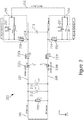
Fig. 2 shows a circuit diagram of an example RF energy harvesting apparatus such as the example apparatus ofFig. 1 ; -
Fig. 3 shows a plan view of an example RF energy harvesting apparatus such as the RF energy harvesting apparatus ofFigs. 1 and2 ; -
Fig. 4 shows a schematic plan view of another example RF energy harvesting apparatus comprising an RF-to-DC converter comprising a single rectifying arm and a low-pass filter; -
Fig. 5 shows schematic diagrams of how the properties of an example RF-to-DC converter can be adjusted using lumped components; -
Fig. 6 shows a graph displaying the results of a simulation comparing the conversion of AC to DC of the RF-to-DC converter when the inductive element shown inFigs. 1 ,2 and3 is present and is not present; -
Fig. 7 shows a schematic diagram of a low-pass filter according to examples of the disclosure; and -
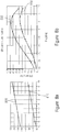
Fig. 8 shows two graphs displaying the improvement in conversion of AC to DC of the RF-to-DC converter when using the low-pass filter of examples of the disclosure. - In the drawings like reference numerals are used to indicate like elements.
- Aspects of the disclosure relate to a converter for converting a received radio frequency signal into a DC signal for powering a load. The converter comprises a first rectifying arm for generating a DC signal based on a first RF voltage input obtained from the received RF signal, and a second rectifying arm for generating a DC signal based on a second RF voltage input obtained from the received RF signal.
- The received RF signal provides the voltage difference between the first RF voltage input and the second RF voltage input, and each rectifying arm comprises a rectifier arranged to generate, based on its RF voltage input, the DC signal and one or more harmonics of its RF voltage input, and to output the DC signal and the one or more harmonics together with a component of its RF voltage input. Each rectifying arm also comprises a first planar transmission line arranged to guide its RF voltage input to the rectifier, and a second planar transmission line arranged to receive from the rectifier the DC signal, the component of its RF voltage input and the one or more harmonics from the rectifier, and to reflect the one or more harmonics back towards the rectifier.
- The first planar transmission line is further arranged to reflect back towards the rectifier radio frequency signals from the rectifier that are based on the reflected signals. The first planar transmission line of the first rectifying arm is connected to the first planar transmission line of the second rectifying arm by a connection which comprises an inductor to allow DC current to flow between the first rectifier arm and the second rectifier arm.
- Aspects of the disclosure also relate to a converter for converting a received radio frequency signal into a DC signal for powering a load. The converter comprises a first rectifying arm for generating a DC signal based on a first RF voltage input obtained from the received RF signal, and a second rectifying arm for generating a DC signal based on a second RF voltage input obtained from the received RF signal.
- The received RF signal provides the voltage difference between the first RF voltage input and the second RF voltage input. Each rectifying arm comprises a rectifier arranged to generate, based on its RF voltage input, the DC signal and one or more harmonics of its RF voltage input, and to output the DC signal and the one or more harmonics together with a component of its RF voltage input. Each rectifying arm also comprises a first planar transmission line arranged to guide its RF voltage input to the rectifier, and a second planar transmission line arranged to receive from the rectifier the DC signal, the component of its RF voltage input and the one or more harmonics from the rectifier, and to reflect the one or more harmonics back towards the rectifier.
- The first planar transmission line is further arranged to reflect back towards the rectifier radio frequency signals from the rectifier that are based on the reflected signals. A connection is provided between the first planar transmission line of the first rectifying arm and the first planar transmission line of the second rectifying arm, and the connection comprises a capacitor.
- Aspects of the disclosure also relate to a converter for converting a received radio frequency signal into a DC signal for powering a load. The converter comprises a rectifier arranged to generate, based on the radio frequency signal, the DC signal and one or more harmonics of the radio frequency signal, and to output the DC signal and the one or more harmonics together with a component of the radio frequency signal.
- The converter also comprises a first planar transmission line arranged to guide the received radio frequency signal to the rectifier, and a second planar transmission line arranged to receive from the rectifier the DC signal, the component of the radio frequency signal and the one or more harmonics from the rectifier, and to reflect the one or more harmonics back towards the rectifier. The first planar transmission line is further arranged to reflect back towards the rectifier radio frequency signals from the rectifier that are based on the reflected signals.
- The converter further comprises a low-pass filter for supplying the DC signal to the load, the low-pass filter comprising a filter inductor in series with the load, a third planar transmission line that connects the second transmission line to the filter inductor, and an output stage capacitor having a first plate coupled to the third transmission line and the filter inductor and a second plate coupled to a reference voltage.
- Rectifiers (e.g. diodes) that may be used in wireless energy harvesting to rectify received RF signal can be non-linear devices that generate various harmonics of the RF signal (i.e. a first harmonic at 2f0, a second harmonic at 3f0, etc. of the RF signal having fundamental frequency f0), as well as the DC component that is required to power a load circuit (e.g. a power management module or a battery charging circuit). These harmonics, as well as a component of the fundamental of the received RF signal that propagates through the rectifier, may be prevented from passing from the rectifier to the load by a simple filter circuit that provides a path to ground for these high-frequency signals. The present inventors have recognised that this approach has the draw-back of unnecessarily reducing the efficiency of the RF-to-DC converter, as it effectively discards RF signals whose power could be harnessed.
- More particularly, the present inventors have devised an RF-to-DC converter having a reflective structure that can effectively confine most or all of the harmonic components generated by the rectifier to the vicinity of the rectifier, forcing the harmonics and signals based thereon to propagate through the rectifier multiple times, thus contributing to the DC signal output by the rectifier and consequently increasing the efficiency of the RF-to-DC converter. More specifically, in an example described herein below, the reflective structure comprises a converter comprising two rectifying arms, each rectifying arm having a first and a second planar transmission line with a respective rectifier coupled therebetween, each of these transmission lines being configured to reflect harmonics received from the rectifier back towards the rectifier.
- The RF-to-DC converter of some examples may use lumped components enabling a significant size reduction. In addition, as will be explained in more detail below, because the planar transmission lines of each rectifying arm may be coupled via a connection, properties of that connection (for example, its location or capacitance) and/or the properties of the planar transmission lines themselves (as well as other properties of the RF-to-DC converter 200) can be tuned to suppress harmonics of the RF signal, as will be described in more detail with reference to
Fig. 5 . - Because the RF-to-DC converter of some examples comprises a first planar transmission line of a first rectifying arm connected to a first planar transmission line of a second rectifying arm by a connection, for example which comprises an inductor, it may allow DC current to flow between the first rectifier arm and the second rectifier arm. For example, the inductor may provide isolation at RF work frequency. It may also provide a short circuit between the differential arms, enabling a DC reference for each rectifier of each rectifying arm. Use of the connection comprising an inductor may also improve RF-to-DC conversion, as will be described in more detail with reference to
Fig. 6 . - The reflective structure of some examples of the disclosure also has a low-pass filter comprising a filter inductor in series with the load, a third planar transmission line that connects the second transmission line to the filter inductor, and an output stage capacitor having a first plate coupled to the third transmission line and the filter inductor and a second plate coupled to a reference voltage. The low pass filter may be configured to allow the DC component to be extracted from the reflective structure whilst having little or no effect on the reflection of the harmonics within the reflective structure.
- As will be explained in the following, this reflective structure can effectively make the RF impedance of the rectifier independent of the input impedance of a load circuit that may be connected to the output of the RF-to-DC converter, allowing the converter to perform efficient RF-to-DC conversion for a variety of different loads or a variable load.
- An example RF-to-DC converter is shown schematically in
Fig. 1 , in a circuit diagram inFig. 2 and also in plan view inFig. 3 .Figs. 1 to 3 show an RF-to-DC converter 200 coupled at one end to anantenna 100. The other end of the RF-to-DC converter 200 is coupled to aload 300. The RF-to-DC converter is fabricated from a conductive track printed on a substrate such as a circuit board, for example an FR-4 board. The conductive track forming the RF-to-DC converter may be provided by the same type of conductive track which makes up theantenna 100. - The RF-to-DC converter comprises two rectifying
arms arm arm 207 is oriented in a different direction to the rectifier of theother arm 209. Examples of rectifying elements suitable for use as rectifier 220 include semiconductor devices such as diodes, and in the present example, each rectifier 220 is a Schottky diode. Other examples include the parasitic or inherent diode provided by a transistor, or a gate-source coupled transistor. Each rectifyingarm planar transmission line arm planar transmission line low pass filter 250. - The first
planar transmission line 210a of thefirst rectifying arm 207 is connected to the firstplanar transmission line 210b of thesecond rectifying arm 209 by a connection which comprises aninductive element 205, such as a lumped component, for example an inductor, connected between the input couplings of the tworectifier arms first rectifier arm 207 and thesecond rectifier arm 209. In the present example, theinductive element 205 comprises an inductor having an inductance of 270 nH. It will of course be understood that in other examples aninductive element 205 is not necessary, and the connection could be replaced by a transmission line such as a stripline or any other conductive link or frequency selective component. - A low-
pass filter 250 comprising afilter inductor 256 and a thirdplanar transmission line 254 connects the second transmission line 230 of eachrectifying arm load 300 via thefilter inductor 256. A respective low-pass filter rectifying arm filter inductor 256 of each low-pass filter inductive element 205 and is a 270 nH inductor, although an inductor having an inductance greater than or less than 270 nH may alternatively be used, for example a 100 nH inductor may be used. The low-pass filter 250 also comprises a lumped component, in this example comprising anoutput stage capacitor 257 having a first plate coupled to thethird transmission line 254 and thefilter inductor 256 and a second plate coupled to a reference voltage, which in the present example comprises a virtual ground. - The first 210, second 230 and third 254 planar transmission lines may take one of many different forms known to those skilled in the art. For example, each of the first, second and third planar transmission lines may be a stripline, microstrip, slotline, coplanar waveguide and a coplanar stripline transmission line, or a combination of two or more of these kinds of transmission line. However, in the present example, each of the first, second and third planar transmission lines takes the form of a microstrip transmission line comprising a respective conductive track that is formed on a first side of an insulating substrate, wherein a conductive layer providing a ground plane common to all three transmission lines is formed on an opposite side of the substrate.
- The conductive track forming part of the microstrip of each of the first, second and
third transmission lines 210, 230, 254 may, as in the present example, be provided in the form of a 35 µm thick copper layer formed on a substrate. Naturally, a metal or another conductive material other than copper may be used instead, and the thickness of the conductive trace may be varied, for example in the range between 9 µm and 70 µm. - In the present example, the tracks which make up the
rectifier arms arms - A
connection planar transmission line 210a of thefirst rectifying arm 207 and the firstplanar transmission line 210b of the second rectifying arm 207b. In the present example, there are twoconnections planar transmission line 210a of the first rectifying arm 207a and the firstplanar transmission line 210b of thesecond rectifying arm 209. Eachconnection 212, 215 may comprise a lumped component, for example a capacitor, and may have the same capacitance or a differing capacitance as each other. In the example shown, eachconnection arms - At least one of the properties of the
transmission lines planar transmission lines connections Fig. 5 , at least one property, for example the dimensions, of the conductive traces forming the microstrips of the first and/orsecond transmission lines second transmission lines second transmission lines connection - In the present example, the dimensions of the conductive traces forming the microstrips of the
first transmission lines connection Fig. 3 , there is a step change in the thickness of thefirst transmission lines connections rectifiers connections capacitor - The first
planar transmission line arm antenna 100 and to guide the received RF signals to the rectifier 220. The rectifier 220 of eacharm planar transmission line - In examples where the rectifier 220 receives a first RF signal in a first RF band and a second RF signal in a second RF band via the
antenna 100 and the first planar transmission line 210, for example, the rectifier 220 is arranged to generate, based on the first and second RF signals, the DC signal and two or more harmonics of each of the first and second RF signals during operation of the RF-to-DC converter. In this case, the first planar transmission line 210 may be arranged to receive a component of each of the harmonics generated by the rectifier 220 during operation of the RF-to-DC converter. - In the example shown, both the first transmission line 210 and the second transmission line 230 of each
rectifying arm connections converter 200 is consequently increased in relation to a conventional RF-to-DC converter not having the reflective structure of the present example. - The low-
pass filter 250 is arranged to transmit the DC signal and to substantially block any RF signals which reach this stage of theconverter 200, including a component of the received RF signals and the harmonics of the received RF signals. - In use, the first
planar transmission line arm antenna 100 and guides the received RF signals to each respective rectifier 220. Therectifier arm planar transmission line 230a, 230b. DC current flows between the two rectifyingarms inductive element 205, providing a DC reference for eachrectifier - The DC signal, the fundamental component of the RF signal, and one or more harmonics of the RF signal all pass to the corresponding second
planar transmission line rectifier rectifier connections rectifier rectifier rectifier DC converter 200. As noted above, the harmonics are reflected back towards each correspondingrectifier rectifier DC converter 200. - As will be explained in more detail below with reference to
Fig. 5 , by using lumped components for theconnections connections - The differential DC signal produced by each two rectifying
arms pass filter 250. The differential DC signal passes from eachsecond transmission line rectifier arm respective filter inductor third transmission line 254 and then on to acommon load 300. Theoutput stage capacitor 257 which has a first plate coupled to the third transmission line and thefilter inductor 256, and a second plate coupled to a reference voltage. The low-pass filter 250 may be configured to allow the differential DC signal component to be extracted from the reflective structure whilst having little or no effect on the reflection of the harmonics within the reflective structure. - As shown in
Figs. 7 and8 , providing theoutput stage capacitor 257 as part of the low-pass filter 250 in this way may address issues of self-resonance of the low-pass filter 250 and/or may improve RF isolation. For example, the low-pass filter 250 may reduce interference between the rectifiers 220 and theload 300. For example, the inductance of thefilter inductor 256, and the capacitance of theoutput stage capacitor 257 may be selected to adjust the self-resonant frequency of the low-pass filter 250. -
Fig. 7a shows an example low-pass filter that does not comprise theoutput stage capacitor 257 as described above, andFig. 7b shows an example that does comprise an output stage capacitor 257 (for example as used in the low-pass filter 250 described above in relation toFigs. 1 to 3 ).Fig. 8 shows the results of simulations conducted comparing the two apparatus illustrated inFigs. 7a and 7b . The lines indicated by thenumbers Fig. 7b with the output stage capacitor, and the lines indicated by thenumbers Fig. 7a , without the output stage capacitor. - It can be seen that the use of the output stage capacitor (in this example a 10pF capacitor) as illustrated in
Fig. 7b helps to increase RF isolation as shown by the graph ofFig. 8a , as the low capacitance represents a low RF impedance to the ground. It can be seen that the RF level is 40dB lower using the low-pass filter ofFig. 7b . This enhancement produces an immediate positive impact: less interference between rectifier 220 andload 300. The use of the low-pass filter ofFig. 7b may also improve efficiency as illustrated inFig. 8b , which shows the rectifier efficiency curb with the apparatus ofFig. 7a (represented by line 860) compared to that of the apparatus ofFig. 7b (represented by the line 850). - The
second transmission line rectifying arm single rectifying arm Figs. 1 ,2 and3 comprises aninductor Figs. 1 ,2 and3 may be removed, replaced or combined. For example, it will be appreciated that thisinductor rectifying arm Fig. 5 . - In some examples, the two rectifying
arms capacitor 216, 316 as shown inFigs. 1 ,2 and3 . Thecapacitor 216, 316 may reduce AC ripple from the DC output of therectifiers arms capacitor 216, 316 may be replaced by some other form of conductive link. - Although
Figs. 1 ,2 and3 show eachrectifying arm pass filter 250, it will be appreciated that the low-pass filter 250 described above may be used in examples where the RF-to-DC converter only comprises one rectifying arm, for example as shown inFig. 4. Fig. 4 shows an RF-to-DC converter comprising an input matching network 410 (for example comprising the first transmission line 210 described above in relation toFigs. 1 to 3 ), coupled in series to arectifying component 420 such as a diode, for example a Schottky diode as described above, in turn coupled in series to an output matching network 430 (for example comprising the second transmission line 230 described above in relation toFigs. 1 to 3 ). Theoutput matching network 430 is in turn coupled to a low-pass filter 450 (for example the low-pass filter 250 described above in relation toFigs. 1 to 3 ). - As noted above, the use of lumped components (such as inductors, capacitors) instead of distributed elements (such as stubs, lines) may reduce the footprint of the RF-to-
DC converter 200.Fig. 5 helps to illustrate how the impedance of the RF-to-DC converter may be tuned (for example to match the impedance of the antenna) through the use of lumped components (for example off-the-shelf components) and if necessary further tuned by adjusting properties of the transmissions lines 210, 230. For example,Fig. 5a shows a portion of an RF-to-DC converter comprising a stub.Fig. 5b shows an example of the transmission line ofFig. 5a with elements replaced by lumped components - in this case a connection to a reference voltage via a 1.2 pF capacitor and the inclusion of a 1.5 nH inductor. The waveguiding properties of the transmission line can then be altered (for example by adjusting the dimensions of the transmission lines) to reach the selected impedance to match that of the antenna, for example theantenna 100 illustrated inFig. 1 . Similarly,Fig. 5d illustrates how the properties of the transmission line ofFig. 5c can be adjusted or tuned by including a lumped component (in this case a 5.1 nH inductor) and then by further adjusting the properties of the transmission lines themselves. - It will also be understood that in some examples, not all features of the RF-to-
DC converter 200 may be present. For example, in some examples, the RF-to-DC converter 200 may not comprise aninductive element 205 and//or may not comprise anoutput stage capacitor 257. - In the examples shown, the RF-to-
DC converter 200 is configured to efficiently rectify RF signals in the UHF frequency band (300 MHz to 3 GHz, for example the 900 MHz GSM band), although it may also be configured to operate in one or more of the VHF band (30 MHz to 300 MHz), the UHF frequency band and the SHF frequency band (3 GHz to 30 GHz), based on design considerations such as the dimensions of thetransmission lines 210, 230, 254 and/or theconnections - The RF-to-
DC converter 200 described above may be a single-band converter arranged to efficiently rectify an RF signal in only a single RF band (e.g. a GSM band or a WiFi band). In these cases, the first planar transmission line 210 may be provided with one or more connections comprising acapacitor rectifying arm rectifying arm - In other examples, the RF-to-
DC converter 200 may be configured as a dual-band converter, to efficiently convert a first RF signal in a first frequency band and a second RF signal in a second frequency band that is separate from the first frequency band into the DC signal. In other words, the RF-to-DC converter 200 may be configured to convert RF signals in two different frequency bands spanning respective non-overlapping frequency ranges (i.e. ranges having no common value) to generate the DC signal. As an example, the RF-to-DC converter 200 may be optimised to convert a first RF signal of frequency 2.45 GHz in the WiFi band (2.4 GHz to 2.495 GHz) and a second RF signal of frequency 1.840 GHz in the GSM band (1.805 GHz to 1.880 GHz) into a DC signal for powering theload 300. Signals in these frequency bands are of particular interest as they are widely used for wireless communications and are present at appreciable power levels in many populated areas. As such, they tend to provide a reliable source of RF energy. The RF-to-DC converter 200 may be optimised to convert both the aforementioned RF signals with high efficiency when received at a power level of approximately - 20 dBm, which is expected to occur in many practical applications, although it is also capable of converting such RF signals with power levels at or below zero dBm. As noted above, the RF-to-DC converter 200 may alternatively be configured as a single-band converter, and tuned to perform RF-to-DC conversion of RF signals in a single RF frequency band. - The
antenna 100 may be any antenna suitable for receiving the first and second RF signals, and is preferably impedance-matched to the input impedance of the RF-to-DC converter 200, in order to maximise power transferred to the converter. In examples of the present disclosure, theantenna 100 may be a dual-band antenna arranged to receive RF signals in one or two frequency bands (for example, the 2.4 GHz WiFi (RTM) band (spanning 2.4 GHz to 2.495 GHz) and/or the 1.8 GHz GSM band, which is between 1.805 GHz and 1.880 GHz). At both of these frequencies, the impedance of the antenna is around 100 Ω. Theantenna 100 is preferably as described in UKpatent application GB 15 135 65.0 - The
antenna 100 and therectifiers arms planar transmission lines antenna 100 and therectifiers rectifiers antenna 100. - The
rectifiers - In some embodiments the thickness of the substrate is selected to provide a particular guided wavelength λg. The substrate may comprise an electrical insulator such as a dielectric laminate material, which may comprise a thermoset plastic. Such a substrate may have a loss tangent of between 0.02 and 0.05 at the frequency bands of the antenna. These frequency bands may comprise the 2.4 GHz WiFi band (spanning 2.4 GHz to 2.495 GHz) and the 900 MHz GSM band. The substrate may have a loss tangent of between 0.003 and 0.004 at these frequencies, for example 0.0035. The substrate may have a relative permittivity of between 2.17 to 10.2, for example between 3 and 6, for example about 5, for example 4.8. The substrate may be rigid. For example it may have a Young's modulus of at least 1GPa, for example at least 5 GPa, for example at least 10 GPa, for example less than 40GPa, for example less than 25GPa. The substrate may have a young's modulus of between 10 GPa and 30GPa, for example between 20GPa and 25GPa. One example of such a material is FR-4 glass epoxy. In the present case the substrate is 0.5 mm thick.
- It will, of course, be appreciated that this example of a material is given by way of example only, and that other substrate materials (e.g. RO4003® produced by Rogers Corp.™, which has a relative permittivity of 3.55 and a loss tangent of 0.0027 at these frequencies, or a RO3000® series high-frequency laminate) may be used.
- The substrate may be at least 50 µm thick, for example at least 100 µm thick, for example between 100 µm and 3 mm, for example between 0.125 mm and 1.52 mm. In an example the substrate is rigid and is 0.75mm thick.
- In some examples the substrate may be flexible, for example it may have a young's modulus of less than 1 GPa. In some embodiments the substrate may be resilient, for example it may be configured so that the antenna tends to recover its shape after deformation.
- The substrate may be flat, or may be shaped according to the shape of the energy source from which it is intended to harvest power. For example, the substrate can be shaped so as to form a part of the housing of an electronic device. For example, it may be shaped to provide a clip-on case for a device such as a cellular telephone or tablet computer.
- In addition to mounting on telephone handsets, power harvesting apparatus of the present disclosure may be provided in, or as accessories to any of a wide variety of sources of RF energy. Some may be provided in heat resistant cases or in mechanically robust and/or water resistant cases to enable them to be integrated into machinery such as internal combustion engines.
- The substrate may be more rigid than the conductive track e.g. to provide mechanical support to the loops, but in some embodiments it may be flexible and/or resilient.
- The RF-to-
DC converter 200 and/or theantenna 100, or any component thereof, may be manufactured by subtractive or additive processes. It may also be manufactured by assembling pre-manufactured components together such as by adhering a conductive sheetlike element to the substrate. This may be done by laying down a preformed track of the conductive material, or by laying down a larger sheet and then etching it away. This sheetlike element may be grown or deposited as a layer on the substrate. If it is deposited a mask may be used so the deposition happens only on regions which are to carry the conductive track and/or it may be allowed to take place over a larger area and then selectively etched away. - Other methods of manufacture may also be used. For example, the antenna may be manufactured by way of '3D printing' whereby a three-dimensional model of the antenna is supplied, in machine readable form, to a '3D printer' adapted to manufacture the antenna. This may be by additive means such as extrusion deposition, Electron Beam Freeform Fabrication (EBF), granular materials binding, lamination, photopolymerization, or stereolithography or a combination thereof. The machine readable model comprises a spatial map of the object to be printed, typically in the form of a Cartesian coordinate system defining the object's surfaces. This spatial map may comprise a computer file which may be provided in any one of a number of file conventions. One example of a file convention is a STL (STereoLithography) file which may be in the form of ASCII (American Standard Code for Information Interchange) or binary and specifies areas by way of triangulated surfaces with defined normals and vertices. An alternative file format is AMF (Additive Manufacturing File) which provides the facility to specify the material and texture of each surface as well as allowing for curved triangulated surfaces. The mapping of the antenna may then be converted into instructions to be executed by 3D printer according to the printing method being used. This may comprise splitting the model into slices (for example, each slice corresponding to an x-y plane, with successive layers building the z dimension) and encoding each slice into a series of instructions. The instructions sent to the 3D printer may comprise Numerical Control (NC) or Computer NC (CNC) instructions, preferably in the form of G-code (also called RS-274), which comprises a series of instructions regarding how the 3D printer should act. The instructions vary depending on the type of 3D printer being used, but in the example of a moving printhead the instructions include: how the printhead should move, when / where to deposit material, the type of material to be deposited, and the flow rate of the deposited material. In some embodiments the power harvesting antenna may be encapsulated in a flexible case, for example a polycarbonate case.
- The tracks of the RF-to-
DC converter 200 may be deposited or printed and other components, such as therectifier - The RF-to-
DC converter 200 as described herein may be embodied in one such machine readable model, for example a machine readable map or instructions, for example to enable a physical representation of said antenna to be produced by 3D printing. This may be in the form of a software code mapping of the antenna and/or instructions to be supplied to a 3D printer (for example numerical code). - In the context of the present disclosure other examples and variations of the apparatus and methods described herein will be apparent to a person of skill in the art.
- Described herein is a converter for converting a received differential radio frequency, RF, signal into a DC signal for powering a load, wherein the received differential RF signal provides a voltage difference between a first RF voltage input and a second RF voltage input. The converter comprises a first rectifying arm for generating a DC signal based on a signal obtained from the first RF voltage input, and a second rectifying arm for generating a DC signal based on a signal obtained from the second RF voltage input, wherein each rectifying arm comprises:
- a rectifier arranged to generate, based on its RF voltage input, the DC signal and one or more harmonics of its RF voltage input, and to output the DC signal and the one or more harmonics together with a component of its RF voltage input;
- a first planar transmission line arranged to guide its RF voltage input to the rectifier; and
- a second planar transmission line arranged to receive from the rectifier the DC signal, the component of its RF voltage input and the one or more harmonics from the rectifier, and to reflect the one or more harmonics back towards the rectifier;
- wherein the first planar transmission line is further arranged to reflect back towards the rectifier radio frequency signals from the rectifier that are based on the reflected signals; and
- The first rectifier arm and the second rectifier arm may each comprise an input coupling for connecting the first planar transmission line of each arm to its RF voltage input, and the inductor is connected between the input couplings of the two rectifier arms.
- The inductor may comprise a lumped component.
- Also described herein is a converter for converting a received differential radio frequency, RF, signal into a DC signal for powering a load, wherein the received differential RF signal provides a voltage difference between a first RF voltage input and a second RF voltage input, the converter comprising:
- a first rectifying arm for generating a DC signal based on a signal obtained from the first RF voltage input, and
- a second rectifying arm for generating a DC signal based on a signal obtained from the second RF voltage input,
- wherein each rectifying arm comprises:
- a rectifier arranged to generate, based on its RF voltage input, the DC signal and one or more harmonics of its RF voltage input, and to output the DC signal and the one or more harmonics together with a component of its RF voltage input;
- a first planar transmission line arranged to guide its RF voltage input to the rectifier; and
- a second planar transmission line arranged to receive from the rectifier the DC signal, the component of its RF voltage input and the one or more harmonics from the rectifier, and to reflect the one or more harmonics back towards the rectifier;
- wherein the first planar transmission line is further arranged to reflect back towards the rectifier radio frequency signals from the rectifier that are based on the reflected signals; and
- At least one of the capacitance of the capacitor, the capacitance of the first planar transmission line, the inductance of the first planar transmission line, and the dimensions of the first planar transmission line maybe selected to reflect back towards the rectifier the radio frequency signals from the rectifier that are based on the reflected signals.
- The position of the connection may be selected to reflect back towards the rectifier the radio frequency signals from the rectifier that are based on the reflected signals.
- The capacitor may comprise a lumped component.
- The converter may comprise two of said connections, wherein each of said connections comprises a respective capacitor.
- The capacitances may be different from each other.
- The capacitances may be selected based on the frequencies of the one or more harmonics.
- The first planar transmission line of the first rectifying arm may be connected to the first planar transmission line of the second rectifying arm by a further connection which comprises an inductor to allow DC current to flow between the first rectifier arm and the second rectifier arm.
- The first rectifier arm and the second rectifier arm may each comprise an input coupling for connecting the first planar transmission line of each arm to its RF voltage input, and the inductor is connected between the input couplings of the two rectifier arms.
- The inductor may comprise a lumped component.
- The converter may comprise a low-pass filter for supplying the DC signal to the load, the low-pass filter comprising a filter inductor in series with the load, a third planar transmission line that connects the second transmission line to the filter inductor, and an output stage capacitor having a first plate coupled to the third transmission line and the filter inductor and a second plate coupled to a reference voltage.
- The output stage capacitor may comprise a lumped component.
- The reference voltage may be ground.
- The low pass filter may be arranged to transmit the DC signal and to substantially block the component of the radio frequency signal and the harmonics of the radio frequency signal.
Claims (15)
- A converter (200) for converting a received radio frequency, RF, signal into a DC signal for powering a load, the converter comprising:a first rectifying arm (207) for generating a DC signal based on a first RF voltage input obtained from the received RF signal, anda second rectifying arm (209) for generating a DC signal based on a second RF voltage input obtained from the received RF signal,wherein the received RF signal provides a voltage difference between the first RF voltage input and the second RF voltage input, and each rectifying arm comprises:a rectifier (220a,220b) arranged to generate, based on its RF voltage input, the DC signal and one or more harmonics of its RF voltage input, and to output the DC signal and the one or more harmonics together with a component of its RF voltage input;a first planar transmission line (210a, 210b) arranged to guide its RF voltage input to the rectifier; anda second planar transmission (230a, 230b) line arranged to receive from the rectifier the DC signal, the component of its RF voltage input and the one or more harmonics from the rectifier, and to reflect the one or more harmonics back towards the rectifier;wherein the first planar transmission line (210a, 210b) is further arranged to reflect back towards the rectifier radio frequency signals from the rectifier thatare based on the reflected signals; andwherein the first planar transmission line of the first rectifying arm is connected to the first planar transmission line of the second rectifying arm by a connection which comprises an inductor (205) to allow DC current to flow between the first rectifier arm and the second rectifier arm.
- The converter of claim 1 wherein the first rectifier arm and the second rectifier arm each comprise an input coupling for connecting the first planar transmission line of each arm to its RF voltage input, and the inductor is connected between the input couplings of the two rectifier arms.
- The converter of claim 2 wherein the inductor comprises a lumped component.
- A converter (200) for converting a received radio frequency, RF, signal into a DC signal for powering a load, the converter comprising:a first rectifying arm (207) for generating a DC signal based on a first RF voltage input obtained from the received RF signal, anda second rectifying arm (209) for generating a DC signal based on a second RF voltage input obtained from the received RF signal,wherein the received RF signal provides a voltage difference between the first RF voltage input and the second RF voltage input, and each rectifying arm comprises:a rectifier (220a,220b) arranged to generate, based on its RF voltage input, the DC signal and one or more harmonics of its RF voltage input, and to output the DC signal and the one or more harmonics together with a component of its RF voltage input;a first planar transmission line (210a, 210b) arranged to guide its RF voltage input to the rectifier; anda second planar transmission line (230a,230b) arranged to receive from the rectifier the DC signal, the component of its RF voltage input and the one or more harmonics from the rectifier, and to reflect the one or more harmonics back towards the rectifier;wherein the first planar transmission line (210a, 210b) is further arranged to reflect back towards the rectifier radio frequency signals from the rectifier thatare based on the reflected signals; andwherein a connection is provided between the first planar transmission line of the first rectifying arm and the first planar transmission line of the second rectifying arm, and the connection comprises a capacitor.
- The converter of claim 4 wherein at least one of the capacitance of the capacitor, the capacitance of the first planar transmission line, the inductance of the first planar transmission line, and the dimensions of the first planar transmission line are selected to reflect back towards the rectifier the radio frequency signals from the rectifier that are based on the reflected signals.
- The converter of claim 4 or 5 wherein the position of the connection is selected to reflect back towards the rectifier the radio frequency signals from the rectifier that are based on the reflected signals.
- The converter of claim 5 or 6 wherein the capacitor comprises a lumped component.
- The converter of any of claims 4 to 7 comprising two of said connections, wherein each of said connections comprises a respective capacitor.
- The converter of claim 8 wherein the capacitances are different from each other for example, wherein the capacitances are selected based on the frequencies of the one or more harmonics.
- The converter of any of claims 4 to 9 wherein the first planar transmission line of the first rectifying arm is connected to the first planar transmission line of the second rectifying arm by a further connection which comprises an inductor to allow DC current to flow between the first rectifier arm and the second rectifier arm.
- The converter of claim 10 wherein the first rectifier arm and the second rectifier arm each comprise an input coupling for connecting the first planar transmission line of each arm to its RF voltage input, and the inductor is connected between the input couplings of the two rectifier arms for example, wherein the inductor comprises a lumped component.
- The converter of any preceding claim further comprising a low-pass filter for supplying the DC signal to the load, the low-pass filter comprising a filter inductor in series with the load, a third planar transmission line that connects the second transmission line to the filter inductor, and an output stage capacitor having a first plate coupled to the third transmission line and the filter inductor and a second plate coupled to a reference voltage for example wherein the output stage capacitor comprises a lumped component.
- The converter of claim 12 wherein the reference voltage comprises ground.
- The converter of any of claims 12 to 13 wherein the low pass filter is arranged to transmit the DC signal and to substantially block the component of the radio frequency signal and the harmonics of the radio frequency signal.
- An RF energy harvesting apparatus comprising the converter of any of the previous claims.
Applications Claiming Priority (2)
| Application Number | Priority Date | Filing Date | Title |
|---|---|---|---|
| GB1700662.8A GB2558647B (en) | 2017-01-13 | 2017-01-13 | RF to DC converter |
| PCT/GB2018/050092 WO2018130849A1 (en) | 2017-01-13 | 2018-01-12 | Rf-to-dc converter |
Publications (2)
| Publication Number | Publication Date |
|---|---|
| EP3568896A1 EP3568896A1 (en) | 2019-11-20 |
| EP3568896B1 true EP3568896B1 (en) | 2021-12-22 |
Family
ID=58463432
Family Applications (1)
| Application Number | Title | Priority Date | Filing Date |
|---|---|---|---|
| EP18702789.1A Active EP3568896B1 (en) | 2017-01-13 | 2018-01-12 | Rf-to-dc converter |
Country Status (4)
| Country | Link |
|---|---|
| US (1) | US10978917B2 (en) |
| EP (1) | EP3568896B1 (en) |
| GB (1) | GB2558647B (en) |
| WO (1) | WO2018130849A1 (en) |
Families Citing this family (11)
| Publication number | Priority date | Publication date | Assignee | Title |
|---|---|---|---|---|
| WO2018039162A2 (en) | 2016-08-22 | 2018-03-01 | William Marsh Rice University | Systems and methods for wireless treatment of arrhythmias |
| US12320769B2 (en) | 2018-11-19 | 2025-06-03 | The Regents Of The University Of California | Systems and methods for battery-less wirelessly powered dielectric sensors |
| WO2020106862A1 (en) | 2018-11-20 | 2020-05-28 | The Regents Of The University Of California | Systems and methods for controlling wirelessly powered leadless pacemakers |
| US12052533B2 (en) | 2019-07-08 | 2024-07-30 | The Regents Of The University Of California | Systems and methods for long-distance remote sensing with sub-wavelength resolution using a wirelessly-powered sensor tag array |
| JP2023515580A (en) | 2020-02-28 | 2023-04-13 | ザ リージェンツ オブ ザ ユニバーシティ オブ カリフォルニア | Integrated Energy Recovery Transceiver and Transmitter with Dual Antenna Architecture for Microimplants and Electrochemical Sensors |
| CN115335710A (en) * | 2020-03-26 | 2022-11-11 | 株式会社友华 | RF detector and high frequency module having the same |
| JP2022070600A (en) * | 2020-10-27 | 2022-05-13 | キヤノン株式会社 | Wireless power transfer systems, control methods and programs for wireless power transfer systems |
| WO2024015555A1 (en) | 2022-07-14 | 2024-01-18 | Maxwell Biomedical Inc. | Advanced pacing |
| US11990847B2 (en) | 2022-07-19 | 2024-05-21 | King Fahd University Of Petroleum And Minerals | Body biasing of a CMOS rectifier for RF energy harvesting |
| US12362594B2 (en) * | 2022-07-28 | 2025-07-15 | Polyvalor, Limited Partnership | Optimization system and method for radio frequency energy harvesting |
| CN115242064A (en) * | 2022-07-29 | 2022-10-25 | 北京北方华创微电子装备有限公司 | Harmonic suppression circuit, radio frequency power supply and semiconductor process equipment |
Family Cites Families (9)
| Publication number | Priority date | Publication date | Assignee | Title |
|---|---|---|---|---|
| JP3761293B2 (en) * | 1997-08-06 | 2006-03-29 | Necエンジニアリング株式会社 | Rectenna equipment |
| KR101831871B1 (en) * | 2010-12-22 | 2018-02-27 | 인텔렉추얼디스커버리 주식회사 | Wireless energy collection apparatus and wireless electronic label adopting the same |
| GB2517907B (en) * | 2013-08-09 | 2018-04-11 | Drayson Tech Europe Ltd | RF Energy Harvester |
| EP3087660B1 (en) * | 2013-12-12 | 2018-09-19 | The Ohio State Innovation Foundation | Harmonic harvester for improved rf-to-dc rectifying efficiency |
| US9906064B2 (en) * | 2014-09-22 | 2018-02-27 | Qualcomm Technologies International, Ltd. | Receiver circuit |
| US10312743B2 (en) * | 2015-05-26 | 2019-06-04 | King Abdullah University Of Science And Technology | RF-to-DC power converters for wireless powering |
| GB2538576B (en) * | 2015-09-14 | 2017-06-14 | Drayson Tech (Europe) Ltd | RF-to-DC Converter |
| GB2538575B (en) * | 2015-09-14 | 2017-06-14 | Drayson Tech (Europe) Ltd | RF-to-DC Converter |
| KR102084401B1 (en) * | 2016-06-13 | 2020-03-04 | 미쓰비시덴키 가부시키가이샤 | High frequency rectifier |
-
2017
- 2017-01-13 GB GB1700662.8A patent/GB2558647B/en not_active Expired - Fee Related
-
2018
- 2018-01-12 WO PCT/GB2018/050092 patent/WO2018130849A1/en not_active Ceased
- 2018-01-12 US US16/476,637 patent/US10978917B2/en not_active Expired - Fee Related
- 2018-01-12 EP EP18702789.1A patent/EP3568896B1/en active Active
Non-Patent Citations (1)
| Title |
|---|
| None * |
Also Published As
| Publication number | Publication date |
|---|---|
| WO2018130849A1 (en) | 2018-07-19 |
| GB2558647A (en) | 2018-07-18 |
| GB2558647B (en) | 2019-01-02 |
| EP3568896A1 (en) | 2019-11-20 |
| GB201700662D0 (en) | 2017-03-01 |
| US10978917B2 (en) | 2021-04-13 |
| US20190326785A1 (en) | 2019-10-24 |
Similar Documents
| Publication | Publication Date | Title |
|---|---|---|
| EP3568896B1 (en) | Rf-to-dc converter | |
| EP3501058B1 (en) | Apparatus and method for rf energy harvesting | |
| US8610312B2 (en) | Induced power transmission circuit | |
| US9010648B2 (en) | Antenna and RFID tag | |
| EP2251933A1 (en) | Composite antenna | |
| Joseph et al. | Second harmonic exploitation for high-efficiency wireless power transfer using duplexing rectenna | |
| KR20120103501A (en) | Power-receiving device, wireless power-feeding system including power-receiving device, and wireless communication system including power-receiving device | |
| Kim et al. | Highly efficient WPT system with negative impedance converter for Q-factor improvement | |
| US11095165B2 (en) | RF power harvester | |
| US20210119490A1 (en) | An rf power harvesting insert for a wristwatch | |
| Atallah et al. | Novel and compact design of capacitively loaded C-shaped DGS resonators for dual band wireless power transfer (DB-WPT) systems | |
| US20200194874A1 (en) | Loop rectenna | |
| Abdullah et al. | Design of Dual ISM bands low power rectenna for indoor wireless power transfer application | |
| Atallah et al. | Compact coupled resonators for small size dual‐frequency wireless power transfer (DF‐WPT) systems | |
| Shirokova et al. | The system of wireless energy transfer | |
| Wang et al. | Bandwidth enhancement based on optimized via location for multiple vias EBG power/ground planes | |
| Sennouni et al. | Efficient rectenna design incorporating new circularly polarized antenna array for wireless power transmission at 2.45 GHz | |
| JP2015177454A (en) | Multiband antenna | |
| CN207199838U (en) | A kind of two-sided spiral NFC antenna under the environment based on metal | |
| Shirokova et al. | The Study of Operation of the System of Wireless Energy Transfer at Real Conditions | |
| JP2019201520A (en) | Electronic apparatus | |
| Hoang et al. | TLM design of a compact PIFA rectenna | |
| Kaldjob et al. | A low-cost 2.45/5.8 GHz ISM-band rectifier for embedded low-power systems in metallic objects | |
| Yan | The Intelligent Auto-Tracking RF WPT System and Reconfigurable Components | |
| Zulkafli et al. | Integrating Defected Ground Structure in WPT Systems: A Comprehensive Review |
Legal Events
| Date | Code | Title | Description |
|---|---|---|---|
| STAA | Information on the status of an ep patent application or granted ep patent |
Free format text: STATUS: UNKNOWN |
|
| STAA | Information on the status of an ep patent application or granted ep patent |
Free format text: STATUS: THE INTERNATIONAL PUBLICATION HAS BEEN MADE |
|
| PUAI | Public reference made under article 153(3) epc to a published international application that has entered the european phase |
Free format text: ORIGINAL CODE: 0009012 |
|
| STAA | Information on the status of an ep patent application or granted ep patent |
Free format text: STATUS: REQUEST FOR EXAMINATION WAS MADE |
|
| 17P | Request for examination filed |
Effective date: 20190628 |
|
| AK | Designated contracting states |
Kind code of ref document: A1 Designated state(s): AL AT BE BG CH CY CZ DE DK EE ES FI FR GB GR HR HU IE IS IT LI LT LU LV MC MK MT NL NO PL PT RO RS SE SI SK SM TR |
|
| AX | Request for extension of the european patent |
Extension state: BA ME |
|
| DAV | Request for validation of the european patent (deleted) | ||
| DAX | Request for extension of the european patent (deleted) | ||
| STAA | Information on the status of an ep patent application or granted ep patent |
Free format text: STATUS: EXAMINATION IS IN PROGRESS |
|
| 17Q | First examination report despatched |
Effective date: 20200520 |
|
| GRAP | Despatch of communication of intention to grant a patent |
Free format text: ORIGINAL CODE: EPIDOSNIGR1 |
|
| STAA | Information on the status of an ep patent application or granted ep patent |
Free format text: STATUS: GRANT OF PATENT IS INTENDED |
|
| RIC1 | Information provided on ipc code assigned before grant |
Ipc: H02J 50/40 20160101ALI20201218BHEP Ipc: H02J 50/00 20160101ALI20201218BHEP Ipc: H02J 50/20 20160101AFI20201218BHEP |
|
| INTG | Intention to grant announced |
Effective date: 20210121 |
|
| GRAJ | Information related to disapproval of communication of intention to grant by the applicant or resumption of examination proceedings by the epo deleted |
Free format text: ORIGINAL CODE: EPIDOSDIGR1 |
|
| STAA | Information on the status of an ep patent application or granted ep patent |
Free format text: STATUS: EXAMINATION IS IN PROGRESS |
|
| INTC | Intention to grant announced (deleted) | ||
| GRAP | Despatch of communication of intention to grant a patent |
Free format text: ORIGINAL CODE: EPIDOSNIGR1 |
|
| STAA | Information on the status of an ep patent application or granted ep patent |
Free format text: STATUS: GRANT OF PATENT IS INTENDED |
|
| INTG | Intention to grant announced |
Effective date: 20210712 |
|
| GRAS | Grant fee paid |
Free format text: ORIGINAL CODE: EPIDOSNIGR3 |
|
| GRAA | (expected) grant |
Free format text: ORIGINAL CODE: 0009210 |
|
| STAA | Information on the status of an ep patent application or granted ep patent |
Free format text: STATUS: THE PATENT HAS BEEN GRANTED |
|
| RAP3 | Party data changed (applicant data changed or rights of an application transferred) |
Owner name: FREEVOLT TECHNOLOGIES LIMITED |
|
| AK | Designated contracting states |
Kind code of ref document: B1 Designated state(s): AL AT BE BG CH CY CZ DE DK EE ES FI FR GB GR HR HU IE IS IT LI LT LU LV MC MK MT NL NO PL PT RO RS SE SI SK SM TR |
|
| REG | Reference to a national code |
Ref country code: GB Ref legal event code: FG4D |
|
| REG | Reference to a national code |
Ref country code: CH Ref legal event code: EP |
|
| REG | Reference to a national code |
Ref country code: DE Ref legal event code: R096 Ref document number: 602018028472 Country of ref document: DE |
|
| REG | Reference to a national code |
Ref country code: AT Ref legal event code: REF Ref document number: 1457710 Country of ref document: AT Kind code of ref document: T Effective date: 20220115 |
|
| REG | Reference to a national code |
Ref country code: IE Ref legal event code: FG4D |
|
| REG | Reference to a national code |
Ref country code: LT Ref legal event code: MG9D |
|
| PG25 | Lapsed in a contracting state [announced via postgrant information from national office to epo] |
Ref country code: RS Free format text: LAPSE BECAUSE OF FAILURE TO SUBMIT A TRANSLATION OF THE DESCRIPTION OR TO PAY THE FEE WITHIN THE PRESCRIBED TIME-LIMIT Effective date: 20211222 Ref country code: LT Free format text: LAPSE BECAUSE OF FAILURE TO SUBMIT A TRANSLATION OF THE DESCRIPTION OR TO PAY THE FEE WITHIN THE PRESCRIBED TIME-LIMIT Effective date: 20211222 Ref country code: FI Free format text: LAPSE BECAUSE OF FAILURE TO SUBMIT A TRANSLATION OF THE DESCRIPTION OR TO PAY THE FEE WITHIN THE PRESCRIBED TIME-LIMIT Effective date: 20211222 Ref country code: BG Free format text: LAPSE BECAUSE OF FAILURE TO SUBMIT A TRANSLATION OF THE DESCRIPTION OR TO PAY THE FEE WITHIN THE PRESCRIBED TIME-LIMIT Effective date: 20220322 |
|
| REG | Reference to a national code |
Ref country code: NL Ref legal event code: MP Effective date: 20211222 |
|
| REG | Reference to a national code |
Ref country code: AT Ref legal event code: MK05 Ref document number: 1457710 Country of ref document: AT Kind code of ref document: T Effective date: 20211222 |
|
| PG25 | Lapsed in a contracting state [announced via postgrant information from national office to epo] |
Ref country code: SE Free format text: LAPSE BECAUSE OF FAILURE TO SUBMIT A TRANSLATION OF THE DESCRIPTION OR TO PAY THE FEE WITHIN THE PRESCRIBED TIME-LIMIT Effective date: 20211222 Ref country code: NO Free format text: LAPSE BECAUSE OF FAILURE TO SUBMIT A TRANSLATION OF THE DESCRIPTION OR TO PAY THE FEE WITHIN THE PRESCRIBED TIME-LIMIT Effective date: 20220322 Ref country code: LV Free format text: LAPSE BECAUSE OF FAILURE TO SUBMIT A TRANSLATION OF THE DESCRIPTION OR TO PAY THE FEE WITHIN THE PRESCRIBED TIME-LIMIT Effective date: 20211222 Ref country code: HR Free format text: LAPSE BECAUSE OF FAILURE TO SUBMIT A TRANSLATION OF THE DESCRIPTION OR TO PAY THE FEE WITHIN THE PRESCRIBED TIME-LIMIT Effective date: 20211222 Ref country code: GR Free format text: LAPSE BECAUSE OF FAILURE TO SUBMIT A TRANSLATION OF THE DESCRIPTION OR TO PAY THE FEE WITHIN THE PRESCRIBED TIME-LIMIT Effective date: 20220323 |
|
| PG25 | Lapsed in a contracting state [announced via postgrant information from national office to epo] |
Ref country code: NL Free format text: LAPSE BECAUSE OF FAILURE TO SUBMIT A TRANSLATION OF THE DESCRIPTION OR TO PAY THE FEE WITHIN THE PRESCRIBED TIME-LIMIT Effective date: 20211222 |
|
| PG25 | Lapsed in a contracting state [announced via postgrant information from national office to epo] |
Ref country code: SM Free format text: LAPSE BECAUSE OF FAILURE TO SUBMIT A TRANSLATION OF THE DESCRIPTION OR TO PAY THE FEE WITHIN THE PRESCRIBED TIME-LIMIT Effective date: 20211222 Ref country code: SK Free format text: LAPSE BECAUSE OF FAILURE TO SUBMIT A TRANSLATION OF THE DESCRIPTION OR TO PAY THE FEE WITHIN THE PRESCRIBED TIME-LIMIT Effective date: 20211222 Ref country code: RO Free format text: LAPSE BECAUSE OF FAILURE TO SUBMIT A TRANSLATION OF THE DESCRIPTION OR TO PAY THE FEE WITHIN THE PRESCRIBED TIME-LIMIT Effective date: 20211222 Ref country code: PT Free format text: LAPSE BECAUSE OF FAILURE TO SUBMIT A TRANSLATION OF THE DESCRIPTION OR TO PAY THE FEE WITHIN THE PRESCRIBED TIME-LIMIT Effective date: 20220422 Ref country code: ES Free format text: LAPSE BECAUSE OF FAILURE TO SUBMIT A TRANSLATION OF THE DESCRIPTION OR TO PAY THE FEE WITHIN THE PRESCRIBED TIME-LIMIT Effective date: 20211222 Ref country code: EE Free format text: LAPSE BECAUSE OF FAILURE TO SUBMIT A TRANSLATION OF THE DESCRIPTION OR TO PAY THE FEE WITHIN THE PRESCRIBED TIME-LIMIT Effective date: 20211222 Ref country code: CZ Free format text: LAPSE BECAUSE OF FAILURE TO SUBMIT A TRANSLATION OF THE DESCRIPTION OR TO PAY THE FEE WITHIN THE PRESCRIBED TIME-LIMIT Effective date: 20211222 |
|
| PG25 | Lapsed in a contracting state [announced via postgrant information from national office to epo] |
Ref country code: PL Free format text: LAPSE BECAUSE OF FAILURE TO SUBMIT A TRANSLATION OF THE DESCRIPTION OR TO PAY THE FEE WITHIN THE PRESCRIBED TIME-LIMIT Effective date: 20211222 Ref country code: AT Free format text: LAPSE BECAUSE OF FAILURE TO SUBMIT A TRANSLATION OF THE DESCRIPTION OR TO PAY THE FEE WITHIN THE PRESCRIBED TIME-LIMIT Effective date: 20211222 |
|
| REG | Reference to a national code |
Ref country code: CH Ref legal event code: PL |
|
| REG | Reference to a national code |
Ref country code: DE Ref legal event code: R097 Ref document number: 602018028472 Country of ref document: DE |
|
| PG25 | Lapsed in a contracting state [announced via postgrant information from national office to epo] |
Ref country code: MC Free format text: LAPSE BECAUSE OF FAILURE TO SUBMIT A TRANSLATION OF THE DESCRIPTION OR TO PAY THE FEE WITHIN THE PRESCRIBED TIME-LIMIT Effective date: 20211222 Ref country code: IS Free format text: LAPSE BECAUSE OF FAILURE TO SUBMIT A TRANSLATION OF THE DESCRIPTION OR TO PAY THE FEE WITHIN THE PRESCRIBED TIME-LIMIT Effective date: 20220422 |
|
| REG | Reference to a national code |
Ref country code: BE Ref legal event code: MM Effective date: 20220131 |
|
| PLBE | No opposition filed within time limit |
Free format text: ORIGINAL CODE: 0009261 |
|
| STAA | Information on the status of an ep patent application or granted ep patent |
Free format text: STATUS: NO OPPOSITION FILED WITHIN TIME LIMIT |
|
| PG25 | Lapsed in a contracting state [announced via postgrant information from national office to epo] |
Ref country code: LU Free format text: LAPSE BECAUSE OF NON-PAYMENT OF DUE FEES Effective date: 20220112 Ref country code: DK Free format text: LAPSE BECAUSE OF FAILURE TO SUBMIT A TRANSLATION OF THE DESCRIPTION OR TO PAY THE FEE WITHIN THE PRESCRIBED TIME-LIMIT Effective date: 20211222 Ref country code: AL Free format text: LAPSE BECAUSE OF FAILURE TO SUBMIT A TRANSLATION OF THE DESCRIPTION OR TO PAY THE FEE WITHIN THE PRESCRIBED TIME-LIMIT Effective date: 20211222 |
|
| 26N | No opposition filed |
Effective date: 20220923 |
|
| PG25 | Lapsed in a contracting state [announced via postgrant information from national office to epo] |
Ref country code: BE Free format text: LAPSE BECAUSE OF NON-PAYMENT OF DUE FEES Effective date: 20220131 |
|
| PG25 | Lapsed in a contracting state [announced via postgrant information from national office to epo] |
Ref country code: LI Free format text: LAPSE BECAUSE OF NON-PAYMENT OF DUE FEES Effective date: 20220131 Ref country code: CH Free format text: LAPSE BECAUSE OF NON-PAYMENT OF DUE FEES Effective date: 20220131 |
|
| PG25 | Lapsed in a contracting state [announced via postgrant information from national office to epo] |
Ref country code: IE Free format text: LAPSE BECAUSE OF NON-PAYMENT OF DUE FEES Effective date: 20220112 |
|
| PG25 | Lapsed in a contracting state [announced via postgrant information from national office to epo] |
Ref country code: SI Free format text: LAPSE BECAUSE OF FAILURE TO SUBMIT A TRANSLATION OF THE DESCRIPTION OR TO PAY THE FEE WITHIN THE PRESCRIBED TIME-LIMIT Effective date: 20211222 |
|
| PG25 | Lapsed in a contracting state [announced via postgrant information from national office to epo] |
Ref country code: IT Free format text: LAPSE BECAUSE OF FAILURE TO SUBMIT A TRANSLATION OF THE DESCRIPTION OR TO PAY THE FEE WITHIN THE PRESCRIBED TIME-LIMIT Effective date: 20211222 |
|
| P01 | Opt-out of the competence of the unified patent court (upc) registered |
Effective date: 20230518 |
|
| PG25 | Lapsed in a contracting state [announced via postgrant information from national office to epo] |
Ref country code: MK Free format text: LAPSE BECAUSE OF FAILURE TO SUBMIT A TRANSLATION OF THE DESCRIPTION OR TO PAY THE FEE WITHIN THE PRESCRIBED TIME-LIMIT Effective date: 20211222 Ref country code: CY Free format text: LAPSE BECAUSE OF FAILURE TO SUBMIT A TRANSLATION OF THE DESCRIPTION OR TO PAY THE FEE WITHIN THE PRESCRIBED TIME-LIMIT Effective date: 20211222 |
|
| PG25 | Lapsed in a contracting state [announced via postgrant information from national office to epo] |
Ref country code: HU Free format text: LAPSE BECAUSE OF FAILURE TO SUBMIT A TRANSLATION OF THE DESCRIPTION OR TO PAY THE FEE WITHIN THE PRESCRIBED TIME-LIMIT; INVALID AB INITIO Effective date: 20180112 |
|
| PG25 | Lapsed in a contracting state [announced via postgrant information from national office to epo] |
Ref country code: MT Free format text: LAPSE BECAUSE OF FAILURE TO SUBMIT A TRANSLATION OF THE DESCRIPTION OR TO PAY THE FEE WITHIN THE PRESCRIBED TIME-LIMIT Effective date: 20211222 |
|
| PG25 | Lapsed in a contracting state [announced via postgrant information from national office to epo] |
Ref country code: TR Free format text: LAPSE BECAUSE OF FAILURE TO SUBMIT A TRANSLATION OF THE DESCRIPTION OR TO PAY THE FEE WITHIN THE PRESCRIBED TIME-LIMIT Effective date: 20211222 |
|
| PGFP | Annual fee paid to national office [announced via postgrant information from national office to epo] |
Ref country code: GB Payment date: 20260121 Year of fee payment: 9 |
|
| PGFP | Annual fee paid to national office [announced via postgrant information from national office to epo] |
Ref country code: DE Payment date: 20260119 Year of fee payment: 9 |
|
| PGFP | Annual fee paid to national office [announced via postgrant information from national office to epo] |
Ref country code: FR Payment date: 20260128 Year of fee payment: 9 |