EP3567517A1 - Display screen and electronic device - Google Patents
Display screen and electronic device Download PDFInfo
- Publication number
- EP3567517A1 EP3567517A1 EP17890298.7A EP17890298A EP3567517A1 EP 3567517 A1 EP3567517 A1 EP 3567517A1 EP 17890298 A EP17890298 A EP 17890298A EP 3567517 A1 EP3567517 A1 EP 3567517A1
- Authority
- EP
- European Patent Office
- Prior art keywords
- fingerprint recognition
- sub
- pixel
- display screen
- electrode
- Prior art date
- Legal status (The legal status is an assumption and is not a legal conclusion. Google has not performed a legal analysis and makes no representation as to the accuracy of the status listed.)
- Granted
Links
Images




Classifications
-
- G—PHYSICS
- G02—OPTICS
- G02F—OPTICAL DEVICES OR ARRANGEMENTS FOR THE CONTROL OF LIGHT BY MODIFICATION OF THE OPTICAL PROPERTIES OF THE MEDIA OF THE ELEMENTS INVOLVED THEREIN; NON-LINEAR OPTICS; FREQUENCY-CHANGING OF LIGHT; OPTICAL LOGIC ELEMENTS; OPTICAL ANALOGUE/DIGITAL CONVERTERS
- G02F1/00—Devices or arrangements for the control of the intensity, colour, phase, polarisation or direction of light arriving from an independent light source, e.g. switching, gating or modulating; Non-linear optics
- G02F1/01—Devices or arrangements for the control of the intensity, colour, phase, polarisation or direction of light arriving from an independent light source, e.g. switching, gating or modulating; Non-linear optics for the control of the intensity, phase, polarisation or colour
- G02F1/13—Devices or arrangements for the control of the intensity, colour, phase, polarisation or direction of light arriving from an independent light source, e.g. switching, gating or modulating; Non-linear optics for the control of the intensity, phase, polarisation or colour based on liquid crystals, e.g. single liquid crystal display cells
- G02F1/133—Constructional arrangements; Operation of liquid crystal cells; Circuit arrangements
- G02F1/1333—Constructional arrangements; Manufacturing methods
- G02F1/13338—Input devices, e.g. touch panels
-
- G—PHYSICS
- G02—OPTICS
- G02F—OPTICAL DEVICES OR ARRANGEMENTS FOR THE CONTROL OF LIGHT BY MODIFICATION OF THE OPTICAL PROPERTIES OF THE MEDIA OF THE ELEMENTS INVOLVED THEREIN; NON-LINEAR OPTICS; FREQUENCY-CHANGING OF LIGHT; OPTICAL LOGIC ELEMENTS; OPTICAL ANALOGUE/DIGITAL CONVERTERS
- G02F1/00—Devices or arrangements for the control of the intensity, colour, phase, polarisation or direction of light arriving from an independent light source, e.g. switching, gating or modulating; Non-linear optics
- G02F1/01—Devices or arrangements for the control of the intensity, colour, phase, polarisation or direction of light arriving from an independent light source, e.g. switching, gating or modulating; Non-linear optics for the control of the intensity, phase, polarisation or colour
- G02F1/13—Devices or arrangements for the control of the intensity, colour, phase, polarisation or direction of light arriving from an independent light source, e.g. switching, gating or modulating; Non-linear optics for the control of the intensity, phase, polarisation or colour based on liquid crystals, e.g. single liquid crystal display cells
- G02F1/133—Constructional arrangements; Operation of liquid crystal cells; Circuit arrangements
- G02F1/1333—Constructional arrangements; Manufacturing methods
-
- G—PHYSICS
- G02—OPTICS
- G02F—OPTICAL DEVICES OR ARRANGEMENTS FOR THE CONTROL OF LIGHT BY MODIFICATION OF THE OPTICAL PROPERTIES OF THE MEDIA OF THE ELEMENTS INVOLVED THEREIN; NON-LINEAR OPTICS; FREQUENCY-CHANGING OF LIGHT; OPTICAL LOGIC ELEMENTS; OPTICAL ANALOGUE/DIGITAL CONVERTERS
- G02F1/00—Devices or arrangements for the control of the intensity, colour, phase, polarisation or direction of light arriving from an independent light source, e.g. switching, gating or modulating; Non-linear optics
- G02F1/01—Devices or arrangements for the control of the intensity, colour, phase, polarisation or direction of light arriving from an independent light source, e.g. switching, gating or modulating; Non-linear optics for the control of the intensity, phase, polarisation or colour
- G02F1/13—Devices or arrangements for the control of the intensity, colour, phase, polarisation or direction of light arriving from an independent light source, e.g. switching, gating or modulating; Non-linear optics for the control of the intensity, phase, polarisation or colour based on liquid crystals, e.g. single liquid crystal display cells
- G02F1/133—Constructional arrangements; Operation of liquid crystal cells; Circuit arrangements
- G02F1/1333—Constructional arrangements; Manufacturing methods
- G02F1/1335—Structural association of cells with optical devices, e.g. polarisers or reflectors
- G02F1/133509—Filters, e.g. light shielding masks
- G02F1/133514—Colour filters
-
- G—PHYSICS
- G06—COMPUTING OR CALCULATING; COUNTING
- G06V—IMAGE OR VIDEO RECOGNITION OR UNDERSTANDING
- G06V10/00—Arrangements for image or video recognition or understanding
- G06V10/10—Image acquisition
- G06V10/17—Image acquisition using hand-held instruments
-
- G—PHYSICS
- G06—COMPUTING OR CALCULATING; COUNTING
- G06V—IMAGE OR VIDEO RECOGNITION OR UNDERSTANDING
- G06V10/00—Arrangements for image or video recognition or understanding
- G06V10/94—Hardware or software architectures specially adapted for image or video understanding
-
- G—PHYSICS
- G06—COMPUTING OR CALCULATING; COUNTING
- G06V—IMAGE OR VIDEO RECOGNITION OR UNDERSTANDING
- G06V40/00—Recognition of biometric, human-related or animal-related patterns in image or video data
- G06V40/10—Human or animal bodies, e.g. vehicle occupants or pedestrians; Body parts, e.g. hands
- G06V40/12—Fingerprints or palmprints
- G06V40/13—Sensors therefor
- G06V40/1306—Sensors therefor non-optical, e.g. ultrasonic or capacitive sensing
-
- G—PHYSICS
- G06—COMPUTING OR CALCULATING; COUNTING
- G06V—IMAGE OR VIDEO RECOGNITION OR UNDERSTANDING
- G06V40/00—Recognition of biometric, human-related or animal-related patterns in image or video data
- G06V40/10—Human or animal bodies, e.g. vehicle occupants or pedestrians; Body parts, e.g. hands
- G06V40/12—Fingerprints or palmprints
- G06V40/13—Sensors therefor
- G06V40/1318—Sensors therefor using electro-optical elements or layers, e.g. electroluminescent sensing
-
- H—ELECTRICITY
- H10—SEMICONDUCTOR DEVICES; ELECTRIC SOLID-STATE DEVICES NOT OTHERWISE PROVIDED FOR
- H10D—INORGANIC ELECTRIC SEMICONDUCTOR DEVICES
- H10D86/00—Integrated devices formed in or on insulating or conducting substrates, e.g. formed in silicon-on-insulator [SOI] substrates or on stainless steel or glass substrates
- H10D86/40—Integrated devices formed in or on insulating or conducting substrates, e.g. formed in silicon-on-insulator [SOI] substrates or on stainless steel or glass substrates characterised by multiple TFTs
-
- H—ELECTRICITY
- H10—SEMICONDUCTOR DEVICES; ELECTRIC SOLID-STATE DEVICES NOT OTHERWISE PROVIDED FOR
- H10D—INORGANIC ELECTRIC SEMICONDUCTOR DEVICES
- H10D86/00—Integrated devices formed in or on insulating or conducting substrates, e.g. formed in silicon-on-insulator [SOI] substrates or on stainless steel or glass substrates
- H10D86/40—Integrated devices formed in or on insulating or conducting substrates, e.g. formed in silicon-on-insulator [SOI] substrates or on stainless steel or glass substrates characterised by multiple TFTs
- H10D86/60—Integrated devices formed in or on insulating or conducting substrates, e.g. formed in silicon-on-insulator [SOI] substrates or on stainless steel or glass substrates characterised by multiple TFTs wherein the TFTs are in active matrices
-
- G—PHYSICS
- G02—OPTICS
- G02F—OPTICAL DEVICES OR ARRANGEMENTS FOR THE CONTROL OF LIGHT BY MODIFICATION OF THE OPTICAL PROPERTIES OF THE MEDIA OF THE ELEMENTS INVOLVED THEREIN; NON-LINEAR OPTICS; FREQUENCY-CHANGING OF LIGHT; OPTICAL LOGIC ELEMENTS; OPTICAL ANALOGUE/DIGITAL CONVERTERS
- G02F1/00—Devices or arrangements for the control of the intensity, colour, phase, polarisation or direction of light arriving from an independent light source, e.g. switching, gating or modulating; Non-linear optics
- G02F1/01—Devices or arrangements for the control of the intensity, colour, phase, polarisation or direction of light arriving from an independent light source, e.g. switching, gating or modulating; Non-linear optics for the control of the intensity, phase, polarisation or colour
- G02F1/13—Devices or arrangements for the control of the intensity, colour, phase, polarisation or direction of light arriving from an independent light source, e.g. switching, gating or modulating; Non-linear optics for the control of the intensity, phase, polarisation or colour based on liquid crystals, e.g. single liquid crystal display cells
- G02F1/133—Constructional arrangements; Operation of liquid crystal cells; Circuit arrangements
- G02F1/1333—Constructional arrangements; Manufacturing methods
- G02F1/1335—Structural association of cells with optical devices, e.g. polarisers or reflectors
- G02F1/133509—Filters, e.g. light shielding masks
- G02F1/133512—Light shielding layers, e.g. black matrix
-
- G—PHYSICS
- G02—OPTICS
- G02F—OPTICAL DEVICES OR ARRANGEMENTS FOR THE CONTROL OF LIGHT BY MODIFICATION OF THE OPTICAL PROPERTIES OF THE MEDIA OF THE ELEMENTS INVOLVED THEREIN; NON-LINEAR OPTICS; FREQUENCY-CHANGING OF LIGHT; OPTICAL LOGIC ELEMENTS; OPTICAL ANALOGUE/DIGITAL CONVERTERS
- G02F1/00—Devices or arrangements for the control of the intensity, colour, phase, polarisation or direction of light arriving from an independent light source, e.g. switching, gating or modulating; Non-linear optics
- G02F1/01—Devices or arrangements for the control of the intensity, colour, phase, polarisation or direction of light arriving from an independent light source, e.g. switching, gating or modulating; Non-linear optics for the control of the intensity, phase, polarisation or colour
- G02F1/13—Devices or arrangements for the control of the intensity, colour, phase, polarisation or direction of light arriving from an independent light source, e.g. switching, gating or modulating; Non-linear optics for the control of the intensity, phase, polarisation or colour based on liquid crystals, e.g. single liquid crystal display cells
- G02F1/133—Constructional arrangements; Operation of liquid crystal cells; Circuit arrangements
- G02F1/1333—Constructional arrangements; Manufacturing methods
- G02F1/1343—Electrodes
Definitions
- the present invention relates to the field of fingerprint recognition techniques, and in particular to a display screen and electronic device.
- fingerprint recognition technology provides the features of universality, uniqueness, security, collectability, acceptability and so on.
- Fingerprint recognition is based on the fact that different fingerprints have different texture characteristics, and by comparing a plurality of global and detailed features between different fingerprint images, is able to determine the identity of an individual the fingerprint image belongs to.
- the majority of the fingerprint recognition technology does not directly store the fingerprint images, but use a digital fingerprint recognition algorithm to find the characteristics of compared fingerprints.
- fingerprint recognition technologies are divided into optical, capacitive and ultrasonic categories.
- fingerprint recognition is not only widely used in access control and attendance system, but also consumer electronics with the technological development. For example, many smart phones and tablet computers are also equipped with the fingerprint recognition function.
- the traditional optical fingerprint recognition technology is to place the finger under a built-in light source, then using a prism to project the image to the charge coupled device (CCD) to form a grayscale image of interleaved black-and-white ridges and valleys, which can be processed by fingerprint device algorithm.
- CCD charge coupled device
- this is not suitable for many daily applications due to large optical path and equipment size.
- the capacitive fingerprint recognition technology gains attention because of the size.
- the capacitive fingerprint recognition technology is to use the finger as an electrode of the capacitor and the fingerprint sensor as the other electrode to form a grayscale image based on the capacitance difference between the ridge and valley with respect to the smooth fingerprint sensor, and then uses the fingerprint algorithm to match the global and local detailed characteristics of the fingerprints to achieve fingerprint recognition.
- fingerprint recognition function is located gradually from the display screen exterior the display screen interior. That is, the conventional design to placing the fingerprint function at the bottom, side or back of the phone is changed to the integration into the display area of the screen.
- IPS in-plane switching
- a common approach is to use in-plane switching (IPS) technology to add the fingerprint recognition function to the in-cell touch panel to use touch sensor with fingerprint recognition and display time-sharing scanning to achieve integrating the fingerprint recognition into the display area (i.e., touch, display, fingerprint recognition function integrated into one).
- IPS in-plane switching
- touch sensor i.e., touch, display, fingerprint recognition function integrated into one
- display products with low resolution and without embedded touch function such as, a small-sized visual fingerprint reader, a home TV with a fingerprint recognition function, a car display screen, etc., the same method cannot be used to integrate fingerprint recognition into display area.
- the object of the present invention is to provide a display screen, capable of integrating a fingerprint recognition function in a display area having a low resolution and without a touch function, enabling full-screen multi-block fingerprint recognition without time-division scanning, improving fingerprint recognition precision and widening diversity of fingerprint recognition applications, and improving the cost-performance value of traditional display products as well as enhancing the user's experience.
- Another object of the present invention is to provide an electronic device, with a display screen capable of integrating a fingerprint recognition function in a display area having a low resolution and without a touch function, enabling full-screen multi-block fingerprint recognition without time-division scanning, improving fingerprint recognition precision and widening diversity of fingerprint recognition applications, and improving the cost-performance value of traditional display products as well as enhancing the user's experience.
- the present invention provides a display screen, which comprises: a thin film transistor (TFT) array substrate, a color filter (CF) substrate disposed opposite to the TFT array substrate, and a liquid crystal layer sandwiched between the TFT array substrate and the CF substrate;
- the TFT array substrate comprising: a pixel electrode layer and a plurality of fingerprint recognition signal lines, an interlayer insulation layer disposed between the pixel electrode layer and the plurality of fingerprint recognition signal lines;
- the CF substrate comprising a black matrix layer;
- the display screen comprising: an active area, and the active area comprising a plurality of pixel units, with each pixel unit comprising a plurality of sub-pixel units; one or more fingerprint recognition blocks disposed in the active area; in the fingerprint recognition area: the pixel electrode layer corresponding to each sub-pixel unit comprising a sub-pixel electrode and a fingerprint recognition electrode spaced from the sub-pixel electrode; the black matrix layer corresponding to each sub-pixel unit comprising a black frame covering the peripheral of the sub-pixel electrode and
- the fingerprint recognition signal line contacts the fingerprint recognition electrode via a through hole penetrating the interlayer insulation layer to electrically connect the fingerprint recognition electrode to an integrated chip for display and fingerprint recognition.
- the fingerprint recognition signal line is made of a metal material.
- the pixel electrode layer is made of indium tin oxide (ITO).
- the fingerprint recognition block has a rectangular shape, with the edge length of 4mm-5.5mm.
- the pixel electrode layer corresponding to each sub-pixel unit comprises a sub-pixel electrode; and the black matrix layer corresponding to each sub-pixel unit comprises only the black frame covering the sub-pixel electrode peripheral.
- the sub-pixel unit is a red sub-pixel unit, a green sub-pixel unit or a blue sub-pixel unit.
- the present invention further provides an electronic device, which comprises the aforementioned display screen.
- the present invention further provides a display screen, which comprises: a thin film transistor (TFT) array substrate, a color filter (CF) substrate disposed opposite to the TFT array substrate, and a liquid crystal layer sandwiched between the TFT array substrate and the CF substrate;
- the TFT array substrate comprising: a pixel electrode layer and a plurality of fingerprint recognition signal lines, an interlayer insulation layer disposed between the pixel electrode layer and the plurality of fingerprint recognition signal lines;
- the CF substrate comprising a black matrix layer;
- the display screen comprising: an active area, and the active area comprising a plurality of pixel units, with each pixel unit comprising a plurality of sub-pixel units; one or more fingerprint recognition blocks disposed in the active area; in the fingerprint recognition area: the pixel electrode layer corresponding to each sub-pixel unit comprising a sub-pixel electrode and a fingerprint recognition electrode spaced from the sub-pixel electrode;
- the black matrix layer corresponding to each sub-pixel unit comprising a black frame covering the peripheral of the sub-
- the present invention provides a display screen and an electronic device, by disposing a plurality of one or more fingerprint recognition blocks in the active area, with the corresponding pixel electrode layer comprising a sub-pixel electrode and a fingerprint recognition electrode spaced from the sub-pixel electrode, the corresponding black matrix layer comprising a black frame covering the sub-pixel electrode peripheral and a black block covering the fingerprint recognition electrode; and disposing the fingerprint recognition signal lines contacting the fingerprint recognition electrode to electrically connect the fingerprint recognition electrode to an integrated chip for display and fingerprint recognition.
- the invention is capable of integrating a fingerprint recognition function in a display area having a low resolution and without a touch function, enabling full-screen multi-block fingerprint recognition without time-division scanning, improving fingerprint recognition precision and widening diversity of fingerprint recognition applications, and improving the cost-performance value of traditional display products as well as enhancing the user's experience.
- the present invention provides a display screen.
- the display screen comprises: a thin film transistor (TFT) array substrate 1, a color filter (CF) substrate 2 disposed opposite to the TFT array substrate 1, and a liquid crystal layer 3 sandwiched between the TFT array substrate 1 and the CF substrate 2.
- the display screen further comprises a backlight module 6 disposed below the TFT array substrate 1 and an encapsulation cover plate 8 disposed above the CF substrate 2.
- the display screen comprises an active area AA, and the active area AA further comprises a plurality of pixel units P, with each pixel unit P comprising a plurality of sub-pixel units SP.
- the active area AA is disposed with one or more fingerprint recognition blocks 5.
- the TFT array substrate 1 comprises: a pixel electrode layer 11 and a plurality of fingerprint recognition signal lines 13.
- An interlayer insulation layer 12 is disposed between the pixel electrode layer 11 and the plurality of fingerprint recognition signal lines 13.
- a base layer, gate layer, active layer source/drain layer and a plurality of insulation layers are disposed below the pixel electrode layer 11, which is the known technology, and the details is not described here.
- the CF substrate 2 comprises a black matrix layer 21; and further comprises a base layer and a color film layer having red, green and blue color-resist, which is the known technology, and the details is not described here.
- the pixel electrode layer corresponding to each sub-pixel unit is a whole sub-pixel electrode, and the black matrix is only a black frame covering the peripheral of the sub-pixel electrode.
- the pixel electrode layer 11 corresponding to each sub-pixel unit SP comprises a sub-pixel electrode 111 and a fingerprint recognition electrode 112 spaced from the sub-pixel electrode 111;
- the black matrix layer 21 corresponding to each sub-pixel unit 11 comprises a black frame 211 covering the peripheral of the sub-pixel electrode 111 and a black block 212 covering the fingerprint recognition electrode 112;
- the fingerprint recognition signal line 13 contacts the fingerprint recognition electrode112 to electrically connect the fingerprint recognition electrode 112 to an integrated chip 9 for display and fingerprint recognition.
- the pixel electrode layer 11 corresponding to each sub-pixel unit SP comprises only a sub-pixel electrode 111; and the black matrix layer 21 corresponding to each sub-pixel unit SP comprises only the black frame 211 covering the sub-pixel electrode 111 peripheral.
- the sub-pixel electrode 111 in the fingerprint recognition block 5 is used for displaying, and the fingerprint recognition electrode 112 is used for fingerprint recognition.
- the fingerprint recognition signal line 13 is connected to the fingerprint recognition electrode112 and the integrated chip 9 for display and fingerprint recognition to achieve integrating the fingerprint recognition function to the active area AA of the display screen.
- the design of separating the sub-pixel electrode 111 and the fingerprint recognition electrode 112 avoids the interference between the display signal and the fingerprint recognition signal without using time-division scanning, and does not exclude each other to occupy the time resources of the scanning. Instead, the independent scanning between fingerprint recognition and display improves the fingerprint recognition scanning frequency and efficiency, and enables the display screen without high resolution and touch function to provide fingerprint recognition function.
- the pixel electrode layer is preferably made of indium tin oxide (ITO).
- ITO indium tin oxide
- the fingerprint recognition signal line 13 is made of a metal material.
- a deposition and patternizing process is required for forming the fingerprint recognition signal lines 13.
- through holes 122 must be formed on the interlayer insulation layer 12 corresponding to the fingerprint recognition electrode 112.
- the fingerprint recognition signal line 13 contacts the fingerprint recognition electrode 112 via the through holes 122 penetrating the interlayer insulation layer 12 to electrically connect the fingerprint recognition electrode 112 to the integrated chip 9 for display and fingerprint recognition.
- the specific number of the fingerprint recognition blocks 5 is based on satisfying the user experience. For example, disposing five or ten fingerprint recognition blocks can achieve to recognize the fingerprints of all the fingers of one hand or both hands. Also the number of fingers to be checked simultaneously also increases as well as higher fingerprint recognition precision and higher privacy security.
- the size of each fingerprint recognition block 5 is generally designed to be similar to the area of a finger touching the display screen, with a rectangular shape, and the side length of about 4 mm to 5.5 mm.
- Each fingerprint recognition block 5 can correspond to a plurality of pixel units P, and the pixel unit P comprises, but not limited to, a red sub-pixel, a green sub-pixel and a blue sub-pixel.
- each sub-pixel unit SP can be a red sub-pixel, a green sub-pixel or a blue sub-pixel.
- the number of fingerprint electrodes 112 in the fingerprint recognition block 5 required to be connected to the fingerprint recognition signal line 13 can be decided according to the size of the sub-pixel unit SP and the routing difficulty.
- the integrated chip 9 for display and fingerprint recognition covers both the displaying and fingerprint recognition driving function, and is able to save routing space of the display screen and reduce design complexity.
- the operation theory of the fingerprint recognition by the display screen of the present invention is as follows: the plurality of fingerprint recognition electrodes 112 in the TFT array substrate 1 and the ridges and the valleys of the fingerprint form capacitors, and the capacitance difference between neighboring capacitors is used to form grayscale fingerprint images recognizable by the fingerprint algorithm, so as to detect the local feature points of the fingerprint to achieve fingerprint recognition.
- the present invention also provides an electronic device, which comprises the aforementioned display screen, capable of integrating a fingerprint recognition function in a display area having a low resolution and without a touch function, enabling full-screen multi-block fingerprint recognition without time-division scanning, improving fingerprint recognition precision and widening diversity of fingerprint recognition applications, and improving the cost-performance value of traditional display products as well as enhancing the user's experience.
- the present invention provides a display screen and an electronic device, by disposing a plurality of one or more fingerprint recognition blocks in the active area, with the corresponding pixel electrode layer comprising a sub-pixel electrode and a fingerprint recognition electrode spaced from the sub-pixel electrode, the corresponding black matrix layer comprising a black frame covering the sub-pixel electrode peripheral and a black block covering the fingerprint recognition electrode; and disposing the fingerprint recognition signal lines contacting the fingerprint recognition electrode to electrically connect the fingerprint recognition electrode to an integrated chip for display and fingerprint recognition.
- the invention is capable of integrating a fingerprint recognition function in a display area having a low resolution and without a touch function, enabling full-screen multi-block fingerprint recognition without time-division scanning, improving fingerprint recognition precision and widening diversity of fingerprint recognition applications, and improving the cost-performance value of traditional display products as well as enhancing the user's experience.
Landscapes
- Physics & Mathematics (AREA)
- Engineering & Computer Science (AREA)
- General Physics & Mathematics (AREA)
- Nonlinear Science (AREA)
- Theoretical Computer Science (AREA)
- Multimedia (AREA)
- Mathematical Physics (AREA)
- Chemical & Material Sciences (AREA)
- Crystallography & Structural Chemistry (AREA)
- Optics & Photonics (AREA)
- Human Computer Interaction (AREA)
- Software Systems (AREA)
- Liquid Crystal (AREA)
- Devices For Indicating Variable Information By Combining Individual Elements (AREA)
- Image Input (AREA)
- Position Input By Displaying (AREA)
- Collating Specific Patterns (AREA)
Abstract
Description
- The present invention relates to the field of fingerprint recognition techniques, and in particular to a display screen and electronic device.
- The use of fingerprint recognition technology as a biometric recognition technology provides the features of universality, uniqueness, security, collectability, acceptability and so on. Fingerprint recognition is based on the fact that different fingerprints have different texture characteristics, and by comparing a plurality of global and detailed features between different fingerprint images, is able to determine the identity of an individual the fingerprint image belongs to. The majority of the fingerprint recognition technology does not directly store the fingerprint images, but use a digital fingerprint recognition algorithm to find the characteristics of compared fingerprints. According to the different ways of fingerprint collection, fingerprint recognition technologies are divided into optical, capacitive and ultrasonic categories. As the most mature and inexpensive recognition technology in the current biometrics, fingerprint recognition is not only widely used in access control and attendance system, but also consumer electronics with the technological development. For example, many smart phones and tablet computers are also equipped with the fingerprint recognition function.
- The traditional optical fingerprint recognition technology is to place the finger under a built-in light source, then using a prism to project the image to the charge coupled device (CCD) to form a grayscale image of interleaved black-and-white ridges and valleys, which can be processed by fingerprint device algorithm. However, this is not suitable for many daily applications due to large optical path and equipment size. As the smart watch and wearable devices becoming popular, the capacitive fingerprint recognition technology gains attention because of the size. The capacitive fingerprint recognition technology is to use the finger as an electrode of the capacitor and the fingerprint sensor as the other electrode to form a grayscale image based on the capacitance difference between the ridge and valley with respect to the smooth fingerprint sensor, and then uses the fingerprint algorithm to match the global and local detailed characteristics of the fingerprints to achieve fingerprint recognition.
- With the popularity of smart phones and other consumer electronics, fingerprint recognition function is located gradually from the display screen exterior the display screen interior. That is, the conventional design to placing the fingerprint function at the bottom, side or back of the phone is changed to the integration into the display area of the screen. For small-to-medium size electronic devices with high resolution, such as, smart phone and tablet, a common approach is to use in-plane switching (IPS) technology to add the fingerprint recognition function to the in-cell touch panel to use touch sensor with fingerprint recognition and display time-sharing scanning to achieve integrating the fingerprint recognition into the display area (i.e., touch, display, fingerprint recognition function integrated into one). However, for display products with low resolution and without embedded touch function, such as, a small-sized visual fingerprint reader, a home TV with a fingerprint recognition function, a car display screen, etc., the same method cannot be used to integrate fingerprint recognition into display area.
- The object of the present invention is to provide a display screen, capable of integrating a fingerprint recognition function in a display area having a low resolution and without a touch function, enabling full-screen multi-block fingerprint recognition without time-division scanning, improving fingerprint recognition precision and widening diversity of fingerprint recognition applications, and improving the cost-performance value of traditional display products as well as enhancing the user's experience.
- Another object of the present invention is to provide an electronic device, with a display screen capable of integrating a fingerprint recognition function in a display area having a low resolution and without a touch function, enabling full-screen multi-block fingerprint recognition without time-division scanning, improving fingerprint recognition precision and widening diversity of fingerprint recognition applications, and improving the cost-performance value of traditional display products as well as enhancing the user's experience.
- To achieve the above object, the present invention provides a display screen, which comprises: a thin film transistor (TFT) array substrate, a color filter (CF) substrate disposed opposite to the TFT array substrate, and a liquid crystal layer sandwiched between the TFT array substrate and the CF substrate; the TFT array substrate comprising: a pixel electrode layer and a plurality of fingerprint recognition signal lines, an interlayer insulation layer disposed between the pixel electrode layer and the plurality of fingerprint recognition signal lines; the CF substrate comprising a black matrix layer;
the display screen comprising: an active area, and the active area comprising a plurality of pixel units, with each pixel unit comprising a plurality of sub-pixel units; one or more fingerprint recognition blocks disposed in the active area;
in the fingerprint recognition area: the pixel electrode layer corresponding to each sub-pixel unit comprising a sub-pixel electrode and a fingerprint recognition electrode spaced from the sub-pixel electrode; the black matrix layer corresponding to each sub-pixel unit comprising a black frame covering the peripheral of the sub-pixel electrode and a black block covering the fingerprint recognition electrode; the fingerprint recognition signal line contacting the fingerprint recognition electrode to electrically connect the fingerprint recognition electrode to an integrated chip for display and fingerprint recognition. - The fingerprint recognition signal line contacts the fingerprint recognition electrode via a through hole penetrating the interlayer insulation layer to electrically connect the fingerprint recognition electrode to an integrated chip for display and fingerprint recognition.
- The fingerprint recognition signal line is made of a metal material.
- The pixel electrode layer is made of indium tin oxide (ITO).
- The fingerprint recognition block has a rectangular shape, with the edge length of 4mm-5.5mm.
- Outside of the fingerprint recognition block: the pixel electrode layer corresponding to each sub-pixel unit comprises a sub-pixel electrode; and the black matrix layer corresponding to each sub-pixel unit comprises only the black frame covering the sub-pixel electrode peripheral.
- The sub-pixel unit is a red sub-pixel unit, a green sub-pixel unit or a blue sub-pixel unit.
- The present invention further provides an electronic device, which comprises the aforementioned display screen.
- The present invention further provides a display screen, which comprises: a thin film transistor (TFT) array substrate, a color filter (CF) substrate disposed opposite to the TFT array substrate, and a liquid crystal layer sandwiched between the TFT array substrate and the CF substrate; the TFT array substrate comprising: a pixel electrode layer and a plurality of fingerprint recognition signal lines, an interlayer insulation layer disposed between the pixel electrode layer and the plurality of fingerprint recognition signal lines; the CF substrate comprising a black matrix layer;
the display screen comprising: an active area, and the active area comprising a plurality of pixel units, with each pixel unit comprising a plurality of sub-pixel units; one or more fingerprint recognition blocks disposed in the active area;
in the fingerprint recognition area: the pixel electrode layer corresponding to each sub-pixel unit comprising a sub-pixel electrode and a fingerprint recognition electrode spaced from the sub-pixel electrode; the black matrix layer corresponding to each sub-pixel unit comprising a black frame covering the peripheral of the sub-pixel electrode and a black block covering the fingerprint recognition electrode; the fingerprint recognition signal line contacting the fingerprint recognition electrode to electrically connect the fingerprint recognition electrode to an integrated chip for display and fingerprint recognition;
wherein the fingerprint recognition signal line contacts the fingerprint recognition electrode via a through hole penetrating the interlayer insulation layer to electrically connect the fingerprint recognition electrode to an integrated chip for display and fingerprint recognition;
wherein the fingerprint recognition signal line being made of a metal material. - The beneficial effects of the present invention: the present invention provides a display screen and an electronic device, by disposing a plurality of one or more fingerprint recognition blocks in the active area, with the corresponding pixel electrode layer comprising a sub-pixel electrode and a fingerprint recognition electrode spaced from the sub-pixel electrode, the corresponding black matrix layer comprising a black frame covering the sub-pixel electrode peripheral and a black block covering the fingerprint recognition electrode; and disposing the fingerprint recognition signal lines contacting the fingerprint recognition electrode to electrically connect the fingerprint recognition electrode to an integrated chip for display and fingerprint recognition. The invention is capable of integrating a fingerprint recognition function in a display area having a low resolution and without a touch function, enabling full-screen multi-block fingerprint recognition without time-division scanning, improving fingerprint recognition precision and widening diversity of fingerprint recognition applications, and improving the cost-performance value of traditional display products as well as enhancing the user's experience.
- To make the technical solution of the embodiments according to the present invention, a brief description of the drawings that are necessary for the illustration of the embodiments will be given as follows. Apparently, the drawings described below show only example embodiments of the present invention and for those having ordinary skills in the art, other drawings may be easily obtained from these drawings without paying any creative effort.
- In the drawings:
-
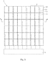
Figure 1 is a schematic view showing the distribution of the fingerprint recognition blocks in the display screen provided by an embodiment of the present invention; -
Figure 2 is a schematic view showing the pixel electrode layer and the black matrix layer in a fingerprint recognition block of the display screen provided by an embodiment of the present invention; -
Figure 3 is a planar view showing the pixel electrode layer and the fingerprint recognition signal line in a fingerprint recognition block of the display screen provided by an embodiment of the present invention; -
Figure 4 is a planar view showing the pixel electrode layer and black matrix layer corresponding to a sub-pixel unit in a fingerprint recognition block of the display screen provided by an embodiment of the present invention; -
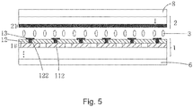
Figure 5 is a cross-sectional view showing the display screen ofFIG. 3 along the B-B direction provided by an embodiment of the present invention; -
Figure 6 is a planar view showing the pixel electrode layer and black matrix layer corresponding to a sub-pixel unit in outside of fingerprint recognition block of the display screen provided by an embodiment of the present invention. - To further explain the technique means and effect of the present invention, the following uses preferred embodiments and drawings for detailed description.
- Referring to
Figure 1 orFigure 6 , the present invention provides a display screen. - As shown in
Figure 5 , the display screen comprises: a thin film transistor (TFT)array substrate 1, a color filter (CF)substrate 2 disposed opposite to theTFT array substrate 1, and aliquid crystal layer 3 sandwiched between theTFT array substrate 1 and theCF substrate 2. Moreover, the display screen further comprises abacklight module 6 disposed below theTFT array substrate 1 and anencapsulation cover plate 8 disposed above theCF substrate 2. - Refer to
Figures 1-4 . The display screen comprises an active area AA, and the active area AA further comprises a plurality of pixel units P, with each pixel unit P comprising a plurality of sub-pixel units SP. The active area AA is disposed with one or morefingerprint recognition blocks 5. - The
TFT array substrate 1 comprises: apixel electrode layer 11 and a plurality of fingerprintrecognition signal lines 13. Aninterlayer insulation layer 12 is disposed between thepixel electrode layer 11 and the plurality of fingerprintrecognition signal lines 13. Moreover, a base layer, gate layer, active layer source/drain layer and a plurality of insulation layers are disposed below thepixel electrode layer 11, which is the known technology, and the details is not described here. - The
CF substrate 2 comprises ablack matrix layer 21; and further comprises a base layer and a color film layer having red, green and blue color-resist, which is the known technology, and the details is not described here. - In the known display screen with fingerprint recognition design, the pixel electrode layer corresponding to each sub-pixel unit is a whole sub-pixel electrode, and the black matrix is only a black frame covering the peripheral of the sub-pixel electrode. However, in the present invention, in the fingerprint recognition area 5: the
pixel electrode layer 11 corresponding to each sub-pixel unit SP comprises asub-pixel electrode 111 and afingerprint recognition electrode 112 spaced from thesub-pixel electrode 111; theblack matrix layer 21 corresponding to eachsub-pixel unit 11 comprises ablack frame 211 covering the peripheral of thesub-pixel electrode 111 and ablack block 212 covering thefingerprint recognition electrode 112; the fingerprintrecognition signal line 13 contacts the fingerprint recognition electrode112 to electrically connect thefingerprint recognition electrode 112 to an integratedchip 9 for display and fingerprint recognition. Outside of the fingerprint recognition block 5: thepixel electrode layer 11 corresponding to each sub-pixel unit SP comprises only asub-pixel electrode 111; and theblack matrix layer 21 corresponding to each sub-pixel unit SP comprises only theblack frame 211 covering thesub-pixel electrode 111 peripheral. - The
sub-pixel electrode 111 in thefingerprint recognition block 5 is used for displaying, and thefingerprint recognition electrode 112 is used for fingerprint recognition. The fingerprintrecognition signal line 13 is connected to the fingerprint recognition electrode112 and the integratedchip 9 for display and fingerprint recognition to achieve integrating the fingerprint recognition function to the active area AA of the display screen. As such, the design of separating thesub-pixel electrode 111 and thefingerprint recognition electrode 112 avoids the interference between the display signal and the fingerprint recognition signal without using time-division scanning, and does not exclude each other to occupy the time resources of the scanning. Instead, the independent scanning between fingerprint recognition and display improves the fingerprint recognition scanning frequency and efficiency, and enables the display screen without high resolution and touch function to provide fingerprint recognition function. - Specifically:
The pixel electrode layer is preferably made of indium tin oxide (ITO). The separation ratio of thesub-pixel electrode 111 and thefingerprint recognition electrode 112 in thefingerprint recognition 5 must make thesub-pixel electrode 111 area as large as possible, on the basis of satisfying the detection requirement of fingerprint recognition, to reduce the loss of pixel aperture rate. - Preferably, the fingerprint
recognition signal line 13 is made of a metal material. A deposition and patternizing process is required for forming the fingerprint recognition signal lines 13. Also, throughholes 122 must be formed on theinterlayer insulation layer 12 corresponding to thefingerprint recognition electrode 112. The fingerprintrecognition signal line 13 contacts thefingerprint recognition electrode 112 via the throughholes 122 penetrating theinterlayer insulation layer 12 to electrically connect thefingerprint recognition electrode 112 to theintegrated chip 9 for display and fingerprint recognition. - The specific number of the fingerprint recognition blocks 5 is based on satisfying the user experience. For example, disposing five or ten fingerprint recognition blocks can achieve to recognize the fingerprints of all the fingers of one hand or both hands. Also the number of fingers to be checked simultaneously also increases as well as higher fingerprint recognition precision and higher privacy security. The size of each
fingerprint recognition block 5 is generally designed to be similar to the area of a finger touching the display screen, with a rectangular shape, and the side length of about 4 mm to 5.5 mm. - Each
fingerprint recognition block 5 can correspond to a plurality of pixel units P, and the pixel unit P comprises, but not limited to, a red sub-pixel, a green sub-pixel and a blue sub-pixel. In other words, each sub-pixel unit SP can be a red sub-pixel, a green sub-pixel or a blue sub-pixel. The number offingerprint electrodes 112 in thefingerprint recognition block 5 required to be connected to the fingerprintrecognition signal line 13 can be decided according to the size of the sub-pixel unit SP and the routing difficulty. - The
integrated chip 9 for display and fingerprint recognition covers both the displaying and fingerprint recognition driving function, and is able to save routing space of the display screen and reduce design complexity. - The operation theory of the fingerprint recognition by the display screen of the present invention is as follows: the plurality of
fingerprint recognition electrodes 112 in theTFT array substrate 1 and the ridges and the valleys of the fingerprint form capacitors, and the capacitance difference between neighboring capacitors is used to form grayscale fingerprint images recognizable by the fingerprint algorithm, so as to detect the local feature points of the fingerprint to achieve fingerprint recognition. - Based on the same theory, the present invention also provides an electronic device, which comprises the aforementioned display screen, capable of integrating a fingerprint recognition function in a display area having a low resolution and without a touch function, enabling full-screen multi-block fingerprint recognition without time-division scanning, improving fingerprint recognition precision and widening diversity of fingerprint recognition applications, and improving the cost-performance value of traditional display products as well as enhancing the user's experience.
- In summary, the present invention provides a display screen and an electronic device, by disposing a plurality of one or more fingerprint recognition blocks in the active area, with the corresponding pixel electrode layer comprising a sub-pixel electrode and a fingerprint recognition electrode spaced from the sub-pixel electrode, the corresponding black matrix layer comprising a black frame covering the sub-pixel electrode peripheral and a black block covering the fingerprint recognition electrode; and disposing the fingerprint recognition signal lines contacting the fingerprint recognition electrode to electrically connect the fingerprint recognition electrode to an integrated chip for display and fingerprint recognition. The invention is capable of integrating a fingerprint recognition function in a display area having a low resolution and without a touch function, enabling full-screen multi-block fingerprint recognition without time-division scanning, improving fingerprint recognition precision and widening diversity of fingerprint recognition applications, and improving the cost-performance value of traditional display products as well as enhancing the user's experience.
- It should be appreciated that the present invention is applied is not limited to the above-described example, those of ordinary skill in the art, can be modified or converted according to the above description, all such modifications and variations shall fall within the appended claims of the invention protected range.
Claims (13)
- A display screen, comprising: a thin film transistor (TFT) array substrate, a color filter (CF) substrate disposed opposite to the TFT array substrate, and a liquid crystal layer sandwiched between the TFT array substrate and the CF substrate; the TFT array substrate comprising: a pixel electrode layer and a plurality of fingerprint recognition signal lines, an interlayer insulation layer disposed between the pixel electrode layer and the plurality of fingerprint recognition signal lines; the CF substrate comprising a black matrix layer;
the display screen comprising: an active area, and the active area comprising a plurality of pixel units, with each pixel unit comprising a plurality of sub-pixel units; one or more fingerprint recognition blocks disposed in the active area;
in the fingerprint recognition area: the pixel electrode layer corresponding to each sub-pixel unit comprising a sub-pixel electrode and a fingerprint recognition electrode spaced from the sub-pixel electrode; the black matrix layer corresponding to each sub-pixel unit comprising a black frame covering the peripheral of the sub-pixel electrode and a black block covering the fingerprint recognition electrode; the fingerprint recognition signal line contacting the fingerprint recognition electrode to electrically connect the fingerprint recognition electrode to an integrated chip for display and fingerprint recognition. - The display screen according to claim 1, wherein the fingerprint recognition signal line contacts the fingerprint recognition electrode via a through hole penetrating the interlayer insulation layer to electrically connect the fingerprint recognition electrode to an integrated chip for display and fingerprint recognition.
- The display screen according to claim 1, wherein the fingerprint recognition signal line is made of a metal material.
- The display screen according to claim 1, wherein the pixel electrode layer is made of indium tin oxide.
- The display screen according to claim 1, wherein the fingerprint recognition block has a rectangular shape, with the edge length of 4mm-5.5mm.
- The display screen according to claim 1, wherein outside of the fingerprint recognition block: the pixel electrode layer corresponding to each sub-pixel unit comprises a sub-pixel electrode; and the black matrix layer corresponding to each sub-pixel unit comprises only the black frame covering the sub-pixel electrode peripheral.
- The display screen according to claim 1, wherein the sub-pixel unit is a red sub-pixel unit, a green sub-pixel unit or a blue sub-pixel unit.
- An electronic device, comprising a display screen according to claim 1.
- A display screen, comprising: a thin film transistor (TFT) array substrate, a color filter (CF) substrate disposed opposite to the TFT array substrate, and a liquid crystal layer sandwiched between the TFT array substrate and the CF substrate; the TFT array substrate comprising: a pixel electrode layer and a plurality of fingerprint recognition signal lines, an interlayer insulation layer disposed between the pixel electrode layer and the plurality of fingerprint recognition signal lines; the CF substrate comprising a black matrix layer;
the display screen comprising: an active area, and the active area comprising a plurality of pixel units, with each pixel unit comprising a plurality of sub-pixel units; one or more fingerprint recognition blocks disposed in the active area;
in the fingerprint recognition area: the pixel electrode layer corresponding to each sub-pixel unit comprising a sub-pixel electrode and a fingerprint recognition electrode spaced from the sub-pixel electrode; the black matrix layer corresponding to each sub-pixel unit comprising a black frame covering the peripheral of the sub-pixel electrode and a black block covering the fingerprint recognition electrode; the fingerprint recognition signal line contacting the fingerprint recognition electrode to electrically connect the fingerprint recognition electrode to an integrated chip for display and fingerprint recognition;
wherein the fingerprint recognition signal line contacts the fingerprint recognition electrode via a through hole penetrating the interlayer insulation layer to electrically connect the fingerprint recognition electrode to an integrated chip for display and fingerprint recognition;
wherein the fingerprint recognition signal line being made of a metal material. - The display screen according to claim 9, wherein the pixel electrode layer is made of indium tin oxide.
- The display screen according to claim 9, wherein the fingerprint recognition block has a rectangular shape, with the edge length of 4mm-5.5mm.
- The display screen according to claim 9, wherein outside of the fingerprint recognition block: the pixel electrode layer corresponding to each sub-pixel unit comprises a sub-pixel electrode; and the black matrix layer corresponding to each sub-pixel unit comprises only the black frame covering the sub-pixel electrode peripheral.
- The display screen according to claim 9, wherein the sub-pixel unit is a red sub-pixel unit, a green sub-pixel unit or a blue sub-pixel unit.
Applications Claiming Priority (2)
| Application Number | Priority Date | Filing Date | Title |
|---|---|---|---|
| CN201710010614.1A CN106815573B (en) | 2017-01-06 | 2017-01-06 | Display screens and electronic devices |
| PCT/CN2017/073883 WO2018126515A1 (en) | 2017-01-06 | 2017-02-17 | Display screen and electronic device |
Publications (3)
| Publication Number | Publication Date |
|---|---|
| EP3567517A1 true EP3567517A1 (en) | 2019-11-13 |
| EP3567517A4 EP3567517A4 (en) | 2020-08-26 |
| EP3567517B1 EP3567517B1 (en) | 2026-04-08 |
Family
ID=59110494
Family Applications (1)
| Application Number | Title | Priority Date | Filing Date |
|---|---|---|---|
| EP17890298.7A Active EP3567517B1 (en) | 2017-01-06 | 2017-02-17 | Display screen and electronic device |
Country Status (6)
| Country | Link |
|---|---|
| US (1) | US10353235B2 (en) |
| EP (1) | EP3567517B1 (en) |
| JP (1) | JP6947828B2 (en) |
| KR (1) | KR102315677B1 (en) |
| CN (1) | CN106815573B (en) |
| WO (1) | WO2018126515A1 (en) |
Families Citing this family (17)
| Publication number | Priority date | Publication date | Assignee | Title |
|---|---|---|---|---|
| CN107450215B (en) * | 2017-08-31 | 2020-07-31 | 厦门天马微电子有限公司 | Array substrate, touch panel, touch display device and driving method thereof |
| US10706304B2 (en) * | 2017-09-28 | 2020-07-07 | Fortinet, Inc. | User authentication via a combination of a fingerprint and a tactile pattern |
| CN108647606B (en) * | 2018-04-28 | 2020-07-14 | 武汉天马微电子有限公司 | A display panel and display device |
| JP6864120B2 (en) * | 2018-09-21 | 2021-04-21 | シェンチェン グディックス テクノロジー カンパニー,リミテッド | Fingerprint recognition device and electronic equipment |
| CN109407818A (en) * | 2018-11-23 | 2019-03-01 | 京东方科技集团股份有限公司 | Touch display screen and its full frame ultrasonic fingerprint identification module |
| CN109828696B (en) * | 2019-01-09 | 2022-09-13 | 广州国显科技有限公司 | Display panel and display screen |
| CN111506208A (en) * | 2019-01-31 | 2020-08-07 | 陕西坤同半导体科技有限公司 | Induction component and full-screen fingerprint touch display panel |
| CN109960331A (en) * | 2019-02-28 | 2019-07-02 | 云谷(固安)科技有限公司 | Show structure, display screen and electronic equipment |
| CN110097023B (en) * | 2019-05-13 | 2023-06-30 | 成都晶砂科技有限公司 | Full-screen fingerprint identification method and display pixel |
| CN110286717B (en) | 2019-06-24 | 2021-07-02 | Oppo广东移动通信有限公司 | Display device, electronic device, and image acquisition method |
| CN110290243B (en) | 2019-06-24 | 2022-07-08 | Oppo广东移动通信有限公司 | Display device, electronic apparatus, and image acquisition method |
| CN110472617B (en) * | 2019-08-29 | 2021-10-12 | 维沃移动通信有限公司 | Display module and electronic equipment |
| CN111240516A (en) * | 2020-01-08 | 2020-06-05 | 武汉华星光电半导体显示技术有限公司 | Touch display panel with fingerprint identification function and touch display device |
| CN114005373B (en) * | 2020-07-16 | 2023-11-03 | 敦泰电子股份有限公司 | Fingerprint display device and integrated circuit for driving same |
| CN112215164B (en) * | 2020-10-14 | 2025-11-18 | 南京欧义光电科技有限公司 | A display screen with integrated fingerprint recognition function |
| CN112748598A (en) * | 2021-01-08 | 2021-05-04 | 武汉华星光电技术有限公司 | Array substrate, display panel and display device |
| CN113433741B (en) * | 2021-06-07 | 2022-08-05 | 武汉华星光电技术有限公司 | Array substrate, manufacturing method of array substrate and display device |
Family Cites Families (27)
| Publication number | Priority date | Publication date | Assignee | Title |
|---|---|---|---|---|
| KR950004378B1 (en) * | 1992-09-09 | 1995-04-28 | 주식회사금성사 | Lcd cell and manufacturing method of situation sensing |
| JP2002159052A (en) * | 2000-11-17 | 2002-05-31 | Nec Kofu Ltd | Mobile terminal with fingerprint authentication function |
| US7053967B2 (en) * | 2002-05-23 | 2006-05-30 | Planar Systems, Inc. | Light sensitive display |
| JP4456806B2 (en) * | 2002-03-19 | 2010-04-28 | セイコーエプソン株式会社 | Liquid crystal display device, electro-optical device and manufacturing method thereof, electronic apparatus |
| KR100436376B1 (en) * | 2002-03-29 | 2004-06-19 | 테스텍 주식회사 | Slim Type Fingerprint Recognition Device Using Contact Light Emitting Device And TFT Fingerprint Input Device |
| KR100992739B1 (en) * | 2004-03-31 | 2010-11-05 | 김영대 | Flat panel device and image pickup method simultaneously with display |
| WO2011104957A1 (en) * | 2010-02-26 | 2011-09-01 | シャープ株式会社 | Display device |
| KR101735386B1 (en) * | 2010-06-25 | 2017-05-30 | 엘지디스플레이 주식회사 | Liquid crystal display device having touch sensor embedded therein, method for driving the same and method for fabricating the same |
| KR20120138887A (en) * | 2011-06-16 | 2012-12-27 | 솔렌시스 주식회사 | Method for detecting pattern using a touch sensor and touch sensor for finger-print recognition |
| KR101524449B1 (en) * | 2011-12-22 | 2015-06-02 | 엘지디스플레이 주식회사 | Liquid crystal display device and Method for manufacturing the same |
| KR102076690B1 (en) * | 2013-04-19 | 2020-02-13 | 삼성디스플레이 주식회사 | Display apparatus |
| KR20150073539A (en) * | 2013-12-23 | 2015-07-01 | 삼성전자주식회사 | Apparatus and method for sensing a touch input in electronic device |
| CN103995634B (en) * | 2014-05-12 | 2017-01-18 | 京东方科技集团股份有限公司 | Touch screen and display device |
| KR20150131944A (en) * | 2014-05-14 | 2015-11-25 | 크루셜텍 (주) | Display apparatus having image scanning function |
| CN104200768A (en) * | 2014-08-18 | 2014-12-10 | 京东方科技集团股份有限公司 | Array substrate, driving method and display device |
| CN104330935B (en) * | 2014-10-10 | 2017-11-14 | 上海天马微电子有限公司 | Array substrate, display panel and display device |
| CN104881196B (en) * | 2015-06-23 | 2018-04-20 | 京东方科技集团股份有限公司 | Substrate and display screen |
| CN104898322B (en) * | 2015-07-09 | 2018-06-15 | 京东方科技集团股份有限公司 | A kind of display device and its driving method |
| CN104934008A (en) * | 2015-07-09 | 2015-09-23 | 京东方科技集团股份有限公司 | Array substrate and driving method thereof, display panel and display apparatus |
| CN105093611B (en) * | 2015-07-21 | 2018-09-11 | 京东方科技集团股份有限公司 | A kind of array substrate and its driving method, display panel, display device |
| CN204965276U (en) * | 2015-09-16 | 2016-01-13 | 昆山龙腾光电有限公司 | Display device with fingerprint identification function |
| CN105930827B (en) * | 2016-05-16 | 2019-03-01 | 京东方科技集团股份有限公司 | Array substrate, display device and driving method thereof |
| CN106022276B (en) * | 2016-05-25 | 2019-06-07 | 京东方科技集团股份有限公司 | Fingerprint recognition device and preparation method thereof, display device, display device |
| CN106096514A (en) * | 2016-06-01 | 2016-11-09 | 京东方科技集团股份有限公司 | Fingerprint identification unit and driving method, display base plate and display device |
| CN106295527B (en) * | 2016-07-29 | 2019-10-15 | 京东方科技集团股份有限公司 | Array substrate, display panel, display device and working method |
| CN106970495A (en) * | 2016-09-14 | 2017-07-21 | 北京小米移动软件有限公司 | Array base palte and preparation method thereof, display panel, display device and electronic equipment |
| TWI616792B (en) * | 2017-05-03 | 2018-03-01 | 友達光電股份有限公司 | Touch display device manufacturing method |
-
2017
- 2017-01-06 CN CN201710010614.1A patent/CN106815573B/en active Active
- 2017-02-17 EP EP17890298.7A patent/EP3567517B1/en active Active
- 2017-02-17 WO PCT/CN2017/073883 patent/WO2018126515A1/en not_active Ceased
- 2017-02-17 JP JP2019537141A patent/JP6947828B2/en active Active
- 2017-02-17 KR KR1020197023082A patent/KR102315677B1/en active Active
- 2017-02-17 US US15/511,017 patent/US10353235B2/en active Active
Also Published As
| Publication number | Publication date |
|---|---|
| KR102315677B1 (en) | 2021-10-20 |
| KR20190104380A (en) | 2019-09-09 |
| WO2018126515A1 (en) | 2018-07-12 |
| EP3567517A4 (en) | 2020-08-26 |
| US20180299725A1 (en) | 2018-10-18 |
| US10353235B2 (en) | 2019-07-16 |
| JP2020506415A (en) | 2020-02-27 |
| CN106815573A (en) | 2017-06-09 |
| EP3567517B1 (en) | 2026-04-08 |
| CN106815573B (en) | 2019-11-19 |
| JP6947828B2 (en) | 2021-10-13 |
Similar Documents
| Publication | Publication Date | Title |
|---|---|---|
| EP3567517B1 (en) | Display screen and electronic device | |
| EP3605207B1 (en) | Array substrate, display screen, and electronic device | |
| US11295107B2 (en) | Display panel | |
| US10643049B2 (en) | Display substrate, manufacturing method thereof, display device and fingerprint identification method | |
| US9940500B2 (en) | Substrate and display panel | |
| US20170371213A1 (en) | Array substrate and drive method thereof, display panel and display device | |
| US10048795B2 (en) | Display device with fingerprint identification and touch detection | |
| US10430013B2 (en) | Touch substrate and manufacturing method thereof, display device, fingerprint determination device and method for determining fingerprint | |
| CN105393261B (en) | Display with Ultrasonic Biometric Sensor in Peripheral Configuration | |
| CN206757648U (en) | Biometric devices and electronic devices | |
| US20180285615A1 (en) | Touch panel and touch display device | |
| CN106775109A (en) | Touch base plate and its driving method, display device | |
| CN107168570A (en) | Array base palte, touch-control display module, electronic equipment and fingerprint identification method | |
| CN107203751B (en) | Display panel and display device | |
| CN107623020A (en) | Display panel, manufacturing method and display device | |
| CN107193430A (en) | Array base palte, display module, electronic equipment, fingerprint identification method and device | |
| US11334740B2 (en) | Circuit, structure, and device for fingerprint recognition, display panel, and display device | |
| KR20140032252A (en) | Display for touch screen and manufacturing method of the same | |
| US11126816B2 (en) | Display device and operation method thereof | |
| CN109031823B (en) | Display screen, electronic device and control method thereof | |
| CN208903234U (en) | Touch screen and electronic equipment | |
| CN112379542A (en) | Display substrate and display device | |
| CN108227994B (en) | Touch panel and driving method thereof, touch display device and fingerprint identification method | |
| TWI792929B (en) | Under-screen fingerprint identification circuit and a laminated structure thereof, display panel and fingerprint capture method | |
| US10782576B2 (en) | Array substrate and driving method thereof |
Legal Events
| Date | Code | Title | Description |
|---|---|---|---|
| STAA | Information on the status of an ep patent application or granted ep patent |
Free format text: STATUS: THE INTERNATIONAL PUBLICATION HAS BEEN MADE |
|
| PUAI | Public reference made under article 153(3) epc to a published international application that has entered the european phase |
Free format text: ORIGINAL CODE: 0009012 |
|
| STAA | Information on the status of an ep patent application or granted ep patent |
Free format text: STATUS: REQUEST FOR EXAMINATION WAS MADE |
|
| 17P | Request for examination filed |
Effective date: 20190805 |
|
| AK | Designated contracting states |
Kind code of ref document: A1 Designated state(s): AL AT BE BG CH CY CZ DE DK EE ES FI FR GB GR HR HU IE IS IT LI LT LU LV MC MK MT NL NO PL PT RO RS SE SI SK SM TR |
|
| AX | Request for extension of the european patent |
Extension state: BA ME |
|
| DAV | Request for validation of the european patent (deleted) | ||
| DAX | Request for extension of the european patent (deleted) | ||
| A4 | Supplementary search report drawn up and despatched |
Effective date: 20200728 |
|
| RIC1 | Information provided on ipc code assigned before grant |
Ipc: H01L 27/12 20060101ALI20200722BHEP Ipc: G06K 9/00 20060101AFI20200722BHEP Ipc: G02F 1/13 20060101ALI20200722BHEP |
|
| STAA | Information on the status of an ep patent application or granted ep patent |
Free format text: STATUS: EXAMINATION IS IN PROGRESS |
|
| RIC1 | Information provided on ipc code assigned before grant |
Ipc: H01L 27/12 20060101ALI20220505BHEP Ipc: G02F 1/1333 20060101ALI20220505BHEP Ipc: G06V 10/10 20220101ALI20220505BHEP Ipc: G06V 40/13 20220101AFI20220505BHEP |
|
| 17Q | First examination report despatched |
Effective date: 20220520 |
|
| REG | Reference to a national code |
Ref country code: DE Ref legal event code: R079 Free format text: PREVIOUS MAIN CLASS: G06K0009000000 Ipc: G06V0040130000 Ref country code: DE Ref legal event code: R079 Ref document number: 602017094749 Country of ref document: DE Free format text: PREVIOUS MAIN CLASS: G06K0009000000 Ipc: G06V0040130000 |
|
| GRAP | Despatch of communication of intention to grant a patent |
Free format text: ORIGINAL CODE: EPIDOSNIGR1 |
|
| STAA | Information on the status of an ep patent application or granted ep patent |
Free format text: STATUS: GRANT OF PATENT IS INTENDED |
|
| RIC1 | Information provided on ipc code assigned before grant |
Ipc: G06V 40/13 20220101AFI20251118BHEP Ipc: G02F 1/1333 20060101ALI20251118BHEP Ipc: H10D 86/40 20250101ALI20251118BHEP Ipc: H10D 86/60 20250101ALI20251118BHEP |
|
| INTG | Intention to grant announced |
Effective date: 20251208 |
|
| GRAS | Grant fee paid |
Free format text: ORIGINAL CODE: EPIDOSNIGR3 |
|
| GRAA | (expected) grant |
Free format text: ORIGINAL CODE: 0009210 |
|
| STAA | Information on the status of an ep patent application or granted ep patent |
Free format text: STATUS: THE PATENT HAS BEEN GRANTED |
|
| AK | Designated contracting states |
Kind code of ref document: B1 Designated state(s): AL AT BE BG CH CY CZ DE DK EE ES FI FR GB GR HR HU IE IS IT LI LT LU LV MC MK MT NL NO PL PT RO RS SE SI SK SM TR |
|
| P01 | Opt-out of the competence of the unified patent court (upc) registered |
Free format text: CASE NUMBER: UPC_APP_0008483_3567517/2026 Effective date: 20260303 |
|
| REG | Reference to a national code |
Ref country code: CH Ref legal event code: F10 Free format text: ST27 STATUS EVENT CODE: U-0-0-F10-F00 (AS PROVIDED BY THE NATIONAL OFFICE) Effective date: 20260408 Ref country code: GB Ref legal event code: FG4D |
|
| REG | Reference to a national code |
Ref country code: DE Ref legal event code: R096 Ref document number: 602017094749 Country of ref document: DE |
|
| REG | Reference to a national code |
Ref country code: IE Ref legal event code: FG4D |