EP3565387A2 - Dehbare elektronik und verfahren zur herstellung davon - Google Patents
Dehbare elektronik und verfahren zur herstellung davon Download PDFInfo
- Publication number
- EP3565387A2 EP3565387A2 EP18210926.4A EP18210926A EP3565387A2 EP 3565387 A2 EP3565387 A2 EP 3565387A2 EP 18210926 A EP18210926 A EP 18210926A EP 3565387 A2 EP3565387 A2 EP 3565387A2
- Authority
- EP
- European Patent Office
- Prior art keywords
- substrate
- input
- output
- devices
- stretchable
- Prior art date
- Legal status (The legal status is an assumption and is not a legal conclusion. Google has not performed a legal analysis and makes no representation as to the accuracy of the status listed.)
- Withdrawn
Links
Images










Classifications
-
- H—ELECTRICITY
- H05—ELECTRIC TECHNIQUES NOT OTHERWISE PROVIDED FOR
- H05K—PRINTED CIRCUITS; CASINGS OR CONSTRUCTIONAL DETAILS OF ELECTRIC APPARATUS; MANUFACTURE OF ASSEMBLAGES OF ELECTRICAL COMPONENTS
- H05K1/00—Printed circuits
- H05K1/02—Details
- H05K1/0277—Bendability or stretchability details
- H05K1/0283—Stretchable printed circuits
-
- B—PERFORMING OPERATIONS; TRANSPORTING
- B06—GENERATING OR TRANSMITTING MECHANICAL VIBRATIONS IN GENERAL
- B06B—METHODS OR APPARATUS FOR GENERATING OR TRANSMITTING MECHANICAL VIBRATIONS OF INFRASONIC, SONIC, OR ULTRASONIC FREQUENCY, e.g. FOR PERFORMING MECHANICAL WORK IN GENERAL
- B06B1/00—Methods or apparatus for generating mechanical vibrations of infrasonic, sonic, or ultrasonic frequency
- B06B1/02—Methods or apparatus for generating mechanical vibrations of infrasonic, sonic, or ultrasonic frequency making use of electrical energy
- B06B1/06—Methods or apparatus for generating mechanical vibrations of infrasonic, sonic, or ultrasonic frequency making use of electrical energy operating with piezoelectric effect or with electrostriction
- B06B1/0688—Methods or apparatus for generating mechanical vibrations of infrasonic, sonic, or ultrasonic frequency making use of electrical energy operating with piezoelectric effect or with electrostriction with foil-type piezoelectric elements, e.g. PVDF
-
- B—PERFORMING OPERATIONS; TRANSPORTING
- B25—HAND TOOLS; PORTABLE POWER-DRIVEN TOOLS; MANIPULATORS
- B25J—MANIPULATORS; CHAMBERS PROVIDED WITH MANIPULATION DEVICES
- B25J13/00—Controls for manipulators
- B25J13/08—Controls for manipulators by means of sensing devices, e.g. viewing or touching devices
- B25J13/081—Touching devices, e.g. pressure-sensitive
- B25J13/084—Tactile sensors
-
- G—PHYSICS
- G01—MEASURING; TESTING
- G01L—MEASURING FORCE, STRESS, TORQUE, WORK, MECHANICAL POWER, MECHANICAL EFFICIENCY, OR FLUID PRESSURE
- G01L1/00—Measuring force or stress, in general
- G01L1/16—Measuring force or stress, in general using properties of piezoelectric devices
-
- G—PHYSICS
- G01—MEASURING; TESTING
- G01L—MEASURING FORCE, STRESS, TORQUE, WORK, MECHANICAL POWER, MECHANICAL EFFICIENCY, OR FLUID PRESSURE
- G01L5/00—Apparatus for, or methods of, measuring force, work, mechanical power, or torque, specially adapted for specific purposes
- G01L5/0061—Force sensors associated with industrial machines or actuators
-
- G—PHYSICS
- G06—COMPUTING OR CALCULATING; COUNTING
- G06F—ELECTRIC DIGITAL DATA PROCESSING
- G06F3/00—Input arrangements for transferring data to be processed into a form capable of being handled by the computer; Output arrangements for transferring data from processing unit to output unit, e.g. interface arrangements
- G06F3/01—Input arrangements or combined input and output arrangements for interaction between user and computer
- G06F3/016—Input arrangements with force or tactile feedback as computer generated output to the user
-
- G—PHYSICS
- G10—MUSICAL INSTRUMENTS; ACOUSTICS
- G10K—SOUND-PRODUCING DEVICES; METHODS OR DEVICES FOR PROTECTING AGAINST, OR FOR DAMPING, NOISE OR OTHER ACOUSTIC WAVES IN GENERAL; ACOUSTICS NOT OTHERWISE PROVIDED FOR
- G10K9/00—Devices in which sound is produced by vibrating a diaphragm or analogous element, e.g. fog horns, vehicle hooters or buzzers
- G10K9/12—Devices in which sound is produced by vibrating a diaphragm or analogous element, e.g. fog horns, vehicle hooters or buzzers electrically operated
- G10K9/122—Devices in which sound is produced by vibrating a diaphragm or analogous element, e.g. fog horns, vehicle hooters or buzzers electrically operated using piezoelectric driving means
- G10K9/125—Devices in which sound is produced by vibrating a diaphragm or analogous element, e.g. fog horns, vehicle hooters or buzzers electrically operated using piezoelectric driving means with a plurality of active elements
-
- H—ELECTRICITY
- H05—ELECTRIC TECHNIQUES NOT OTHERWISE PROVIDED FOR
- H05K—PRINTED CIRCUITS; CASINGS OR CONSTRUCTIONAL DETAILS OF ELECTRIC APPARATUS; MANUFACTURE OF ASSEMBLAGES OF ELECTRICAL COMPONENTS
- H05K1/00—Printed circuits
- H05K1/18—Printed circuits structurally associated with non-printed electric components
- H05K1/181—Printed circuits structurally associated with non-printed electric components associated with surface mounted components
-
- H—ELECTRICITY
- H05—ELECTRIC TECHNIQUES NOT OTHERWISE PROVIDED FOR
- H05K—PRINTED CIRCUITS; CASINGS OR CONSTRUCTIONAL DETAILS OF ELECTRIC APPARATUS; MANUFACTURE OF ASSEMBLAGES OF ELECTRICAL COMPONENTS
- H05K3/00—Apparatus or processes for manufacturing printed circuits
- H05K3/30—Assembling printed circuits with electric components, e.g. with resistors
-
- A—HUMAN NECESSITIES
- A61—MEDICAL OR VETERINARY SCIENCE; HYGIENE
- A61F—FILTERS IMPLANTABLE INTO BLOOD VESSELS; PROSTHESES; DEVICES PROVIDING PATENCY TO, OR PREVENTING COLLAPSING OF, TUBULAR STRUCTURES OF THE BODY, e.g. STENTS; ORTHOPAEDIC, NURSING OR CONTRACEPTIVE DEVICES; FOMENTATION; TREATMENT OR PROTECTION OF EYES OR EARS; BANDAGES, DRESSINGS OR ABSORBENT PADS; FIRST-AID KITS
- A61F2/00—Filters implantable into blood vessels; Prostheses, i.e. artificial substitutes or replacements for parts of the body; Appliances for connecting them with the body; Devices providing patency to, or preventing collapsing of, tubular structures of the body, e.g. stents
- A61F2/02—Prostheses implantable into the body
- A61F2/10—Hair or skin implants
- A61F2/105—Skin implants, e.g. artificial skin
-
- B—PERFORMING OPERATIONS; TRANSPORTING
- B06—GENERATING OR TRANSMITTING MECHANICAL VIBRATIONS IN GENERAL
- B06B—METHODS OR APPARATUS FOR GENERATING OR TRANSMITTING MECHANICAL VIBRATIONS OF INFRASONIC, SONIC, OR ULTRASONIC FREQUENCY, e.g. FOR PERFORMING MECHANICAL WORK IN GENERAL
- B06B1/00—Methods or apparatus for generating mechanical vibrations of infrasonic, sonic, or ultrasonic frequency
- B06B1/02—Methods or apparatus for generating mechanical vibrations of infrasonic, sonic, or ultrasonic frequency making use of electrical energy
- B06B1/06—Methods or apparatus for generating mechanical vibrations of infrasonic, sonic, or ultrasonic frequency making use of electrical energy operating with piezoelectric effect or with electrostriction
- B06B1/0607—Methods or apparatus for generating mechanical vibrations of infrasonic, sonic, or ultrasonic frequency making use of electrical energy operating with piezoelectric effect or with electrostriction using multiple elements
- B06B1/0622—Methods or apparatus for generating mechanical vibrations of infrasonic, sonic, or ultrasonic frequency making use of electrical energy operating with piezoelectric effect or with electrostriction using multiple elements on one surface
- B06B1/0629—Square array
-
- H—ELECTRICITY
- H05—ELECTRIC TECHNIQUES NOT OTHERWISE PROVIDED FOR
- H05K—PRINTED CIRCUITS; CASINGS OR CONSTRUCTIONAL DETAILS OF ELECTRIC APPARATUS; MANUFACTURE OF ASSEMBLAGES OF ELECTRICAL COMPONENTS
- H05K2201/00—Indexing scheme relating to printed circuits covered by H05K1/00
- H05K2201/01—Dielectrics
- H05K2201/0104—Properties and characteristics in general
- H05K2201/0133—Elastomeric or compliant polymer
-
- H—ELECTRICITY
- H05—ELECTRIC TECHNIQUES NOT OTHERWISE PROVIDED FOR
- H05K—PRINTED CIRCUITS; CASINGS OR CONSTRUCTIONAL DETAILS OF ELECTRIC APPARATUS; MANUFACTURE OF ASSEMBLAGES OF ELECTRICAL COMPONENTS
- H05K2201/00—Indexing scheme relating to printed circuits covered by H05K1/00
- H05K2201/09—Shape and layout
- H05K2201/09009—Substrate related
- H05K2201/09045—Locally raised area or protrusion of insulating substrate
-
- H—ELECTRICITY
- H05—ELECTRIC TECHNIQUES NOT OTHERWISE PROVIDED FOR
- H05K—PRINTED CIRCUITS; CASINGS OR CONSTRUCTIONAL DETAILS OF ELECTRIC APPARATUS; MANUFACTURE OF ASSEMBLAGES OF ELECTRICAL COMPONENTS
- H05K2201/00—Indexing scheme relating to printed circuits covered by H05K1/00
- H05K2201/10—Details of components or other objects attached to or integrated in a printed circuit board
- H05K2201/10007—Types of components
- H05K2201/10083—Electromechanical or electro-acoustic component, e.g. microphone
-
- H—ELECTRICITY
- H05—ELECTRIC TECHNIQUES NOT OTHERWISE PROVIDED FOR
- H05K—PRINTED CIRCUITS; CASINGS OR CONSTRUCTIONAL DETAILS OF ELECTRIC APPARATUS; MANUFACTURE OF ASSEMBLAGES OF ELECTRICAL COMPONENTS
- H05K2201/00—Indexing scheme relating to printed circuits covered by H05K1/00
- H05K2201/10—Details of components or other objects attached to or integrated in a printed circuit board
- H05K2201/10007—Types of components
- H05K2201/10151—Sensor
-
- H—ELECTRICITY
- H05—ELECTRIC TECHNIQUES NOT OTHERWISE PROVIDED FOR
- H05K—PRINTED CIRCUITS; CASINGS OR CONSTRUCTIONAL DETAILS OF ELECTRIC APPARATUS; MANUFACTURE OF ASSEMBLAGES OF ELECTRICAL COMPONENTS
- H05K2201/00—Indexing scheme relating to printed circuits covered by H05K1/00
- H05K2201/10—Details of components or other objects attached to or integrated in a printed circuit board
- H05K2201/10431—Details of mounted components
- H05K2201/10507—Involving several components
- H05K2201/10545—Related components mounted on both sides of the PCB
-
- H—ELECTRICITY
- H10—SEMICONDUCTOR DEVICES; ELECTRIC SOLID-STATE DEVICES NOT OTHERWISE PROVIDED FOR
- H10N—ELECTRIC SOLID-STATE DEVICES NOT OTHERWISE PROVIDED FOR
- H10N30/00—Piezoelectric or electrostrictive devices
- H10N30/20—Piezoelectric or electrostrictive devices with electrical input and mechanical output, e.g. functioning as actuators or vibrators
-
- H—ELECTRICITY
- H10—SEMICONDUCTOR DEVICES; ELECTRIC SOLID-STATE DEVICES NOT OTHERWISE PROVIDED FOR
- H10N—ELECTRIC SOLID-STATE DEVICES NOT OTHERWISE PROVIDED FOR
- H10N30/00—Piezoelectric or electrostrictive devices
- H10N30/80—Constructional details
- H10N30/88—Mounts; Supports; Enclosures; Casings
- H10N30/883—Additional insulation means preventing electrical, physical or chemical damage, e.g. protective coatings
Definitions
- the tactile sense refers to the various senses felt through human skin.
- the various types of tactile receptors present under the skin treat various sensations such as a pressure, texture, a temperature, and pain, which are felt on the skin.
- Electro-skin technologies that make feeling of various senses may be expected to be applicable to various industrial fields such as AR/VR fields that provide various senses in virtual environment similar to real world, bio-diagnosis/treatment requiring human tactile ability, healthcare system such as health and medical care such as surgical soft robot, disaster/structure, defense industry, and the like.
- stretchable electronic skin which is similar to human skin, senses tactile information, and outputs the sensed information to the skin, is needed.
- a tactile sensor technology similar to the human skin sensory receptor and an actuator technology capable of transmitting and outputting various senses to human through the skin have to be fused into stretchable electronic skin.
- the present disclosure provides stretchable electronics that senses tactility and transmits stimulation.
- the present disclosure provides a method for fabricating stretchable electronics that senses tactility and transmits stimulation.
- An embodiment of the inventive concept provides stretchable electronics includes: a stretchable substrate; first support patterns disposed on a first surface of the stretchable substrate; and output devices disposed on the first support patterns, respectively, wherein the first support patterns are arranged in a first direction and a second direction, which are parallel to an extension direction of the substrate, and each of the output devices generates an output stimulation.
- the first support patterns may protrude from the first surface of the stretchable substrate.
- each of the first support patterns may have a thickness greater than that of the stretchable substrate.
- the first surface may include a wavy surface.
- the stretchable electronics may further include lines disposed on the stretchable substrate and the first support patterns, wherein the lines may extend along the wavy surface of the first surface.
- the lines may include: first lines extending in the first direction; and second lines extending in the second direction, wherein the output devices may be disposed on areas on which the first lines and the second lines cross each other, respectively.
- At least one of the output devices may include: actuators disposed on the first support patterns; and a diaphragm disposed on the actuators, wherein the diaphragm may be spaced apart from the first support patterns by the actuators, and the diaphragm may vibrate by movement of the actuators.
- the stretchable electronics may further include input devices disposed on the first surface, wherein the input devices and the output devices may be alternately arranged in the first direction and the second direction, and the input devices may sense an input stimulation.
- the stretchable electronics may further include second support patterns disposed between the input devices and the first surface, wherein the second support patterns may protrude from the first surface.
- the stretchable electronics may further include: an output signal control unit; and an input signal control unit, wherein the output devices may generate the output stimulation on the basis of an output signal provided from the output signal control unit, and the input devices may generate input signals corresponding to the input stimulation to provide the input signals to the input signal control unit, wherein the output signal may include position information and intensity information of the output stimulation, and the input signal may include position information and intensity information of the input stimulation.
- each of the second support patterns may be made of a rigid material and include the same material as that within the stretchable substrate.
- the second surface may include a wavy surface.
- a method for fabricating stretchable electronics includes: forming an output device structure on a first carrier substrate; separating the output device structure from the first carrier substrate so as to be transferred to a first surface of the substrate; forming an input device structure on a second carrier substrate; and separating the input device structure from the second carrier substrate so as be transferred to a second surface of the substrate, which faces the first surface, wherein the output device structure comprises output devices generating an output stimulation, and the input device structure comprises input devices receiving an input stimulation.
- the method may further include providing tensile force to the substrate while the output device structure and the input device structure are transferred to the substrate, wherein the substrate may include a pre-stretched substrate.
- FIG. 1 is a block diagram of stretchable electronics according to exemplary embodiments of the inventive concept.
- stretchable electronics including a device unit 2, an input signal control unit 5, and an output signal control unit 6 may be provided.
- the device unit 2 may include an input device part 3 and an output device part 4.
- the input device part 3 may sense an input stimulation.
- the input stimulation may be one of a tactile stimulation, a warm stimulation, a cold stimulation, a nociceptive stimulation, and a tensile stimulation.
- the input device part 3 may generate an input signal corresponding to the input stimulation.
- the input stimulation may be one of a tactile sensation signal, a warm sensation signal, a cold sensation signal, a nociceptive sensation signal, and a tensile sensation signal.
- the input device part 3 may provide an input side to the input signal control unit 5.
- the input signal control unit 5 may generate input data on the basis of the input signal.
- the input data may include a generated position of the input stimulation and intensity information of the input stimulation.
- the input signal control unit 5 may transmit the input data to the outside of the stretchable electronics 1.
- the output device unit 4 may receive an output signal from the output signal control unit 6.
- the output device unit 4 may generate an output stimulation on the basis of the output signal.
- the output stimulation may be one of a tactile stimulation, a warm stimulation, a cold stimulation, a nociceptive stimulation, and a tensile stimulation.
- the output signal may correspond to the output stimulation.
- the output signal may be one of a tactile sensation signal, a warm sensation signal, a cold sensation signal, a nociceptive sensation signal, and a tensile sensation signal.
- the output signal control unit 6 may generate an output signal on the basis of output data.
- the output data may include a generated position of the output stimulation and intensity information of the output stimulation.
- the output signal control unit 6 may receive the output data from the outside of the output signal control unit 6.
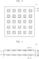
- FIGS. 2 and 3 are plan and bottom views of the stretchable electronics according to exemplary embodiments of the inventive concept.
- FIG. 4 is a cross-sectional view taken along line I-I' of FIGS. 2 and 3 .
- stretchable electronics 10 including a substrate 100, an output control layer 210, output devices 310, a first protection layer 410, an input control layer 220, input devices 510, and a second protection layer 420 may be provided.
- the substrate 100 may be a stretchable substrate.
- the substrate 100 may be stretchable from its initial shape by tensile force. When the tensile force is removed, the substrate 100 may be returned to its initial shape.
- the substrate 100 may have a sufficient thickness to have stretchability.
- the substrate 100 may have a thickness of about 1 ⁇ m to about 2 ⁇ m.
- the substrate 100 may include PI, PDMS, Ecoflex, or a combination thereof.
- the substrate 100 may have a first surface 102 and a second surface 104, which face each other.
- the output control layer 210 may be disposed on the first surface 102.
- the output control layer 210 may have stretchability.
- the output control layer 210 may include output control devices 212 and lines (not shown) electrically connecting the output control devices 212 to each other.
- the output control devices 212 may be arranged in a direction parallel to the first surface 102.
- the output control devices 212 may be electrically connected to the output devices 310 to control the output devices 310.
- the output control devices 212 may receive an output signal from the output signal control unit (see reference numeral 6 of FIG. 1 ) described with reference to FIG. 1 to control the output devices 310 on the basis of the output signal.
- the output devices 310 may be disposed on the output control layer 210. Each of the output devices 310 may extend in parallel to a first incident surface 102.
- the output devices 310 may be controlled by the output control devices 212 to generate the output stimulation. For example, the output devices 310 may generate the tactile stimulation, the warm stimulation, the cold stimulations, the nociceptive stimulation, or the tensile stimulation.
- the output stimulation generated from the output devices 310 may be transmitted to a user using the stretchable electronics 10.
- the first protection layer 410 may be disposed on the output control layer 210 to cover the output devices 310.
- the first protection layer 410 may protect the output control layer 210 and the output devices 310.
- the first protection layer 410 may include an insulation material having the stretchability.
- the input control layer 220 may be disposed on the second surface 104.
- the input control layer 220 may have the stretchability.
- the input control layer 220 may include input control devices 222 and lines (not shown) electrically connecting the input control devices 222 to each other.
- the input control devices 222 may be arranged in a direction parallel to the second surface 104. When the input devices 510 sense the input stimulation, the input control devices 222 may generate an input signal corresponding to the input stimulation.
- the input control devices 222 may be provided in the input signal control unit (see reference numeral 5 of FIG. 1 ) described with reference to FIG. 1 .
- the input devices 510 may be disposed on the input control layer 220.
- the input devices 510 may be arranged in a direction parallel to the second surface 104.
- the input devices 510 may sense an external input stimulation of the input devices 510.
- the input devices 510 may the tactile stimulation, the warm stimulation, the cold stimulations, the nociceptive stimulation, or the tensile stimulation.
- each of the input devices 510 may include a pressure sensitive rubber (PSR) or a piezo-electric layer (PEL).
- PSR pressure sensitive rubber
- PEL piezo-electric layer
- each of the input devices 510 may include a poezoresistive strain sensor.
- the input devices 510 may be electrically connected to the input control devices 222. Thus, when the input devices 510 sense the input stimulation, the input control devices 222 may generate the input signal.
- the second protection layer 420 may be disposed on the input control layer 220 to cover the input devices 510.
- the second protection layer 420 may protect the input control layer 220 and the input devices 510.
- the second protection layer 420 may include an insulation material having the stretchability.
- the stimulation may be outputted and inputted by the output devices 310 and the input device 510 according to the inventive concept.
- Each of the substrate 100, the output control layer 210, the input control layer 220, the first protection layer 410, and the second protection layer 420 may have the stretchability.
- the stretchable electronics 10 may be deformed.
- the stretchable electronics 10 into/from which the stimulation is inputted/outputted may be provided.
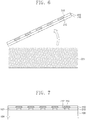
- FIG. 5 is a flowchart for explaining a method for fabricating the stretchable electronics according to exemplary embodiments of the inventive concept.
- FIGS. 6 to 8 are cross-sectional views taken along line I-I' of FIG. 2 so as to explain the method for fabricating the stretchable electronics according to exemplary embodiments of the inventive concept.
- substantially the same description as those described with reference to FIGS. 2 to 4 will be omitted.
- an output control layer 210, output devices 310, and a first protection layer 410 may be formed on a first carrier substrate CS1 (S10).
- the output control layer 210 may include output control devices 212.
- the output control devices 212 may be substantially the same as the output control device 212 described with reference to FIG. 3 .
- the output control layer 210, the output devices 310, and the first protection layer 410 may be detachable from the first carrier substrate CS1 (S20).
- the detachment process may include a process of removing a sacrificial layer (not shown) disposed between the first carrier substrate CS1 and the output control layer 210.
- the output control layer 210, the output devices 310, and the first protection layer 410 may be transferred to the first surface 102 of the substrate 100 (S30).
- the transfer process may include a process of bonding the output control layer 210 to the substrate 100 by using an adhesion layer (not shown).
- the substrate 100 may have stretchability.
- the substrate 100 may be substantially the same as that 100 described with reference to FIGS. 2 to 4 .
- the input control layer 220, the input devices 510, and the second protection layer 420 may be transferred to the second surface 104 of the substrate 100 (S60).
- the transfer process may include a process of bonding the input control layer 220 to the substrate 100 by using an adhesion layer (not shown).
- the stretchable electronics 10 may be provided through the simple process.
- Each of the output devices 310 may include an auxiliary substrate 311, actuators 312, and a diaphragm 313.
- the auxiliary substrate 311 may be disposed on the output control layer 210.
- the auxiliary substrate 311 may be bonded to a top surface of the output control layer 210. That is, a bottom surface of the auxiliary substrate 311 may directly contact the top surface of the output control layer 210.
- the auxiliary substrate 311 may have a rigid material. Thus, when the substrate 100 is deformed, the auxiliary substrate 311 may be maintained in shape without being deformed.
- the auxiliary substrate 311 may include substantially the same material as the substrate 100.
- the auxiliary substrate 311 may include PI, PDMS, Ecoflex, or a combination thereof.
- the auxiliary substrate 311 may have a thickness greater than that of the substrate 100. Since the auxiliary substrate 311 has a rigid property, the auxiliary substrate 311 may have a sufficient thickness.
- the actuators 312 may be disposed on the auxiliary substrate 311.
- the actuators 312 may be spaced apart from each other in a direction parallel to a top surface of the auxiliary substrate 311.
- four actuators 312 disposed adjacent to vertexes of the auxiliary substrate 311 are illustrated in FIG. 9 .
- Each of the actuators 312 may have a size and number, which are selected as desired.
- the actuators 312 may generate vibration.
- each of the actuators 312 may include a piezoelectric element.
- the piezoelectric element may include an upper electrode, a lower electrode, and a piezoelectric thin film disposed between the upper electrode and the lower electrode.
- the upper electrode may be disposed adjacent to the diaphragm 313.
- the lower electrode may be disposed adjacent to the auxiliary substrate 311.
- the piexoelectric thin film may include at least one selected from PZT, PLZT, PMN-PT, PZN-PT, PYN-PT, PIN-PT, PVDF, PVDF-TrFE, PVDF-TFE, PVC, PAN, PPEN, polyamides, ZnO, A1N, BaTiO 3 , LiNbO 3 , and LiTaO3.
- each of the upper electrode and the lower electrode may include at least one selected from ITO, Mo, Al, Ag, Cu, Ti/Au, Ti/Pt, graphene, CNT, metal nanoparticles, PEDOT, and PEDOT-PSS.
- the diaphragm 313 may be disposed on the actuators 312.
- the diaphragm 313 may extend in the direction parallel to the top surface of the auxiliary substrate 311.
- the diaphragm 313 may contact a top surface of each of the actuators 312.
- the diaphragm 313 may contact the upper electrode of each of the actuators 312.
- the diaphragm 313 may overlap the actuators 312 in a direction that is perpendicular to the top surface of the auxiliary substrate 311.
- the diaphragm 313 may be spaced apart from the auxiliary substrate 311 by the actuators 312.
- an air gap may be provided between the diaphragm 313 and the auxiliary substrate 311.
- the diaphragm 313 may include at least one selected from a metal thin film, polyimide, PMMA, PDMS, silicone, and Ecoflex.
- the vibration of the actuator may be absorbed to the stretchable substrate.
- efficiency in which the vibration of the actuators is outputted to the outside of the stretchable electronics may be reduced.
- the auxiliary substrate 311 may not absorb the vibration of the actuators 312. Thus, the vibration output efficiency of the stretchable electronics 11 may be improved.
- FIG. 11 is a cross-sectional view taken along line II-II' of FIG. 9 in the stretchable electronics according to exemplary embodiments of the inventive concept.
- substantially the same description as those described with reference to FIGS. 9 and 10 will be omitted.
- stretchable electronics 12 including a substrate 100, an output control layer 210, output devices 310, a first protection layer 410, an input control layer 220, input devices 510, and a second protection layer 420 may be provided.
- the substrate 100, the output control layer 210, the first protection layer 410, the input control layer 220, and the second protection layer 420 may be substantially the same as the substrate 100, the output control layer 210, the first protection layer 410, the input control layer 220, and the second protection layer 420, which are described with reference to FIGS. 9 and 10 .
- Each of the output devices 310 may include an auxiliary film 314, an actuator 312, and a diaphragm 313.
- the actuator 312 and the diaphragm 313 may be substantially the same as the actuator 312 and the diaphragm 313, which are described with reference to FIGS. 9 and 10 .
- the auxiliary film 314 may be disposed on the output control layer 210.
- the auxiliary film 314 may be bonded to a top surface of the output control layer 210. That is, a bottom surface of the auxiliary film 314 may directly contact the top surface of the output control layer 210.
- the auxiliary film 314 may extend in the direction parallel to the top surface of the output control layer 210.
- the auxiliary film 314 may have a rigid material.
- the auxiliary substrate 311 may include substantially the same material as the substrate 100.
- the auxiliary substrate 311 may include PI, PDMS, Ecoflex, or a combination thereof.
- the auxiliary substrate 311 may have a thickness greater than that of the substrate 100. Since the auxiliary substrate 311 has a rigid property, the auxiliary substrate 311 may have a sufficient thickness.
- the auxiliary film 314 may not absorb the vibration of the actuators 312. Thus, the vibration output efficiency of the stretchable electronics 12 may be improved.
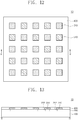
- FIG. 12 is a plan view of stretchable electronics according to exemplary embodiments of the inventive concept.
- FIG. 13 is a cross-sectional view taken along line III-III' of FIG. 12 .
- substantially the same description as those described with reference to FIGS. 2 to 4 will be omitted.
- the output control devices 212 and the input control devices 222 may be alternately arranged in the direction parallel to the top surface of the substrate 100.
- the output control devices 212 may control the output devices 310, respectively.
- the input control devices 222 may control the input devices 510, respectively.
- the output devices 310 and the input devices 510 may be disposed on the control layer 200.
- the output devices 310 and the input devices 510 may be alternately arranged in the direction parallel to the top surface of the substrate 100.
- the output devices 310 and the input devices 510 may be substantially the same as the output devices 310 and the input devices 510, which are described with reference to FIGS. 2 to 4 .
- the stretchable electronics 13 through which the stimulation is outputted and inputted may be provided.
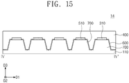
- FIG. 14 is a plan view of stretchable electronics according to exemplary embodiments of the inventive concept.
- FIG. 15 is a cross-sectional view taken along line IV-IV' of FIG. 14 .
- stretchable electronic 14 including a wavy substrate 110, lines 600, support patterns 700, output devices 310, input devices 510, and a protection layer 400 may be provided.
- the wavy substrate 110 may have stretchability. When tensile force is applied to the wavy substrate 110, the wavy substrate 110 may be expanded.
- the wavy substrate 110 may include at least one selected from PDMS, polyimide, PMMA, silicone, and Ecoflex.
- the wavy substrate 110 may a wavy surface.
- the wavy substrate 100 may have a curved top surface. When the wavy substrate 110 is expanded horizontally, wrinkles on the surface of the wavy substrate 110 may be spread.
- the support patterns 700 may be disposed on the wavy substrate 110.
- the support patterns 700 may be arranged in a first direction D1 and a second direction D2, which are parallel to an extension direction of the wavy substrate 110.
- the support patterns 700 may protrude from a top surface of the wavy substrate 110 in a third direction D3 perpendicular to the extension direction of the wavy direction.
- the support patterns 700 may be connected to the wavy substrate 110 without a boundary therebetween.
- Each of the support patterns 700 may have a thickness greater than that of the wavy structure 110.
- a distance between a top surface of the support pattern 700 and the top surface of the wavy substrate 110 may be greater than that between the top surface of the wavy substrate 110 and a bottom surface of the wavy substrate 110. Since each of the support patterns 700 has a rigid property, the support pattern 700 may have a sufficient thickness. Thus, when the wavy substrate 110 is deformed, the support pattern 700 may be maintained in , shape without being deformed.
- the support pattern 700 may include substantially the same material as the wavy substrate 110.
- the wavy substrate 110 may include at least one selected from PDMS, polyimide, PMMA, silicone, and Ecoflex.
- the output devices 310 and the input devices 510 may be disposed on the support patterns 700 different from each other.
- the output devices 310 and the input device 510 may be arranged in the first direction D1 and the second direction D2.
- the output devices may include at least one actuator.
- the actuator When the actuator is directly disposed on the wavy substrate, vibration of the actuator may be absorbed to the wavy substrate. Thus, efficiency in which the vibration of the actuator is outputted to the outside of the stretchable electronics may be reduced.
- the support pattern 700 may not absorb the vibration of the output device 310 including the actuator. Thus, the vibration output efficiency of the stretchable electronics 14 may be improved.
- Output control devices may be disposed between the support patterns 700 and the output devices 310.
- the output control devices may provide an output signal to the output devices 310.
- Input control devices (not shown) may be disposed between the support patterns 700 and the input devices 510.
- the input control devices may generate an input signal.
- the lines 600 may be disposed on the wavy substrate 110 and the support pattern 700.
- the lines 600 may extend along a top surface of the wavy substrate 110 and side and top surfaces of the support pattern 700.
- the lines 600 may extend in the first direction D1 and the second direction D2 and be electrically connected to the output devices 310 and the input devices 510.
- the output devices 310 and the input devices 510 may be disposed on an area on which the lines 600 extending in the different directions cross each other.
- Each of the lines 600 may vibrate in the third direction D3 on the top surface of the wavy substrate 110 and extend in the first direction D1 or the second direction D2.
- each of the lines 600 may decrease in height.
- the lines 600 may be expanded horizontally.
- each of the lines 600 may increase in height.
- the lines 600 may be contracted horizontally.
- the lines 600 may have stretchability.
- the output signal control unit (see reference numeral 6 of FIG. 1 ) described with reference to FIG. 1 applies an output signal to a pair of lines 600, which extend in different directions
- the output device 310 crossing the pair of lines 600 may generate an output stimulation.
- An intensity of the output stimulation may be in proportional to an intensity of the output signal.
- a generated position of the output stimulation and the intensity of the output stimulation may be controlled.
- the input control device may generate an input signal.
- the input signal may be provided to the input signal control unit 5 described with reference to FIG. 1 through the pair of lines 600 crossing the input device 510.
- An intensity of the input signal may be proportional to an intensity of the input stimulation received in the input device 510. As a result, a position of the input stimulation and the intensity of the input stimulation may be measured.
- the stretchable electronics 14 through which the stimulation is outputted and inputted may be provided.
- FIG. 16 is a plan view of a stretchable electronics according to exemplary embodiments of the inventive concept.
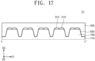
- FIG. 17 is a cross-sectional view taken along line V-V' of FIG. 16 .
- substantially the same description as those described with reference to FIGS. 14 and 15 will be omitted.
- a plurality of devices may be provided on one support pattern 700.
- a structure in which the output device 310 and the input device 510 are disposed on one support pattern 700 is illustrated.
- two or more output devices 310 and/or two or more input devices 510 may be disposed on one support pattern 700.
- the output device 310 and the input device 510, which are disposed on the support pattern 700 may be spaced apart from each other in the first direction parallel to an extension direction of the wavy substrate 110.
- the output device 310 and the input device 510, which are disposed on the support pattern 700 may be electrically connected to each other by the lines 600.
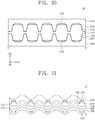
- a lower thin film 820, input devices 510, and a second protection layer 420 may be formed on a second surface 124 of the preliminary wavy substrate 120.
- a process of forming the lower thin film 820, the input devices 510, and the second protection layer 420 may include a process of separating the lower thin film 820 to the second protection layer 420 from a carrier substrate (not shown) so as to be transferred to the second surface 124 of the preliminary wavy substrate 120 after the lower thin film 820, the input devices 510, and the second protection layer 420 are formed on the carrier substrate.
- the preliminary wavy substrate 120 may be subjected to tensile force in the extension direction of the preliminary wavy substrate 120.
- the second surface 124 may be maintained in a flat shape. That is, the preliminary wavy substrate 120 may not have wrinkles.
Landscapes
- Engineering & Computer Science (AREA)
- Physics & Mathematics (AREA)
- Microelectronics & Electronic Packaging (AREA)
- General Physics & Mathematics (AREA)
- General Engineering & Computer Science (AREA)
- Mechanical Engineering (AREA)
- Human Computer Interaction (AREA)
- Theoretical Computer Science (AREA)
- Chemical & Material Sciences (AREA)
- Manufacturing & Machinery (AREA)
- Analytical Chemistry (AREA)
- Multimedia (AREA)
- Robotics (AREA)
- Acoustics & Sound (AREA)
- User Interface Of Digital Computer (AREA)
- Electrotherapy Devices (AREA)
Applications Claiming Priority (1)
| Application Number | Priority Date | Filing Date | Title |
|---|---|---|---|
| KR1020180051480A KR102433137B1 (ko) | 2018-05-03 | 2018-05-03 | 신축성 전자 장치 및 그 제조 방법 |
Publications (2)
| Publication Number | Publication Date |
|---|---|
| EP3565387A2 true EP3565387A2 (de) | 2019-11-06 |
| EP3565387A3 EP3565387A3 (de) | 2019-11-27 |
Family
ID=64949019
Family Applications (1)
| Application Number | Title | Priority Date | Filing Date |
|---|---|---|---|
| EP18210926.4A Withdrawn EP3565387A3 (de) | 2018-05-03 | 2018-12-07 | Dehbare elektronik und verfahren zur herstellung davon |
Country Status (4)
| Country | Link |
|---|---|
| US (1) | US11006520B2 (de) |
| EP (1) | EP3565387A3 (de) |
| KR (1) | KR102433137B1 (de) |
| CN (1) | CN110440959A (de) |
Families Citing this family (7)
| Publication number | Priority date | Publication date | Assignee | Title |
|---|---|---|---|---|
| US12527521B2 (en) | 2013-09-17 | 2026-01-20 | Medibotics Llc | Motion recognition clothing™ with inertial sensors and electrical or optical strain sensors |
| US11071498B2 (en) | 2013-09-17 | 2021-07-27 | Medibotics Llc | Smart clothing with inertial, strain, and electromyographic sensors for human motion capture |
| US11304628B2 (en) | 2013-09-17 | 2022-04-19 | Medibotics Llc | Smart clothing with dual inertial sensors and dual stretch sensors for human motion capture |
| US11892286B2 (en) | 2013-09-17 | 2024-02-06 | Medibotics Llc | Motion recognition clothing [TM] with an electroconductive mesh |
| US10747331B2 (en) * | 2018-07-27 | 2020-08-18 | University Of South Carolina | Virtual reality platform with haptic interface for interfacing with media items having metadata |
| KR102605970B1 (ko) * | 2020-05-25 | 2023-11-29 | 한국전자통신연구원 | 진동 자극 장치 및 이를 포함하는 진동 자극 시스템 |
| US12036175B2 (en) | 2020-05-25 | 2024-07-16 | Electronics And Telecommunications Research Institute | Vibratory stimulation device and vibratory stimulation system including the same |
Family Cites Families (11)
| Publication number | Priority date | Publication date | Assignee | Title |
|---|---|---|---|---|
| US10441185B2 (en) | 2009-12-16 | 2019-10-15 | The Board Of Trustees Of The University Of Illinois | Flexible and stretchable electronic systems for epidermal electronics |
| CN205810862U (zh) * | 2013-03-11 | 2016-12-14 | 苹果公司 | 便携式电子设备及用于便携式电子设备的振动器组件 |
| US9706647B2 (en) * | 2013-05-14 | 2017-07-11 | Mc10, Inc. | Conformal electronics including nested serpentine interconnects |
| KR102104311B1 (ko) * | 2013-11-26 | 2020-04-27 | 한국전자통신연구원 | 전자회로의 제조 방법 |
| KR20160012268A (ko) * | 2014-07-23 | 2016-02-03 | 한국과학기술원 | 다층 그래핀을 이용한 신축성이 높은 전극 및 그 제조방법 |
| US9841548B2 (en) | 2015-06-30 | 2017-12-12 | Apple Inc. | Electronic devices with soft input-output components |
| US10245333B2 (en) | 2015-08-19 | 2019-04-02 | Electronics And Telecommunications Research Institute | Plasma generating apparatus and treatment method using the same |
| KR20170048903A (ko) | 2015-10-27 | 2017-05-10 | 한국전자통신연구원 | 피부 확장 장치 및 이를 이용한 피부 확장 방법 |
| KR102564834B1 (ko) | 2015-11-19 | 2023-08-10 | 한국전자통신연구원 | 피부 확장 장치 및 이를 이용한 피부 확장 방법 |
| WO2017099795A1 (en) * | 2015-12-11 | 2017-06-15 | Intel Corporation | Multi-layer flexible/stretchable electronic package for advanced wearable electronics |
| CN105606291B (zh) | 2016-01-21 | 2018-06-15 | 清华大学 | 热式压力传感器及柔性电子皮肤 |
-
2018
- 2018-05-03 KR KR1020180051480A patent/KR102433137B1/ko active Active
- 2018-12-07 EP EP18210926.4A patent/EP3565387A3/de not_active Withdrawn
- 2018-12-12 US US16/217,629 patent/US11006520B2/en active Active
- 2018-12-13 CN CN201811527661.4A patent/CN110440959A/zh active Pending
Non-Patent Citations (1)
| Title |
|---|
| None |
Also Published As
| Publication number | Publication date |
|---|---|
| KR20190127197A (ko) | 2019-11-13 |
| KR102433137B1 (ko) | 2022-08-19 |
| US11006520B2 (en) | 2021-05-11 |
| EP3565387A3 (de) | 2019-11-27 |
| US20190342993A1 (en) | 2019-11-07 |
| CN110440959A (zh) | 2019-11-12 |
Similar Documents
| Publication | Publication Date | Title |
|---|---|---|
| US11006520B2 (en) | Stretchable electronics and method for fabricating the same | |
| Zhu et al. | Technologies toward next generation human machine interfaces: From machine learning enhanced tactile sensing to neuromorphic sensory systems | |
| JP4922482B2 (ja) | 圧電性ファイバおよび圧電性織物デバイス | |
| Dahiya et al. | Tactile sensing—from humans to humanoids | |
| CN111051834A (zh) | 电容式和触觉传感器及相关感测方法 | |
| JP7184289B2 (ja) | 配線基板及び配線基板の製造方法 | |
| US9971441B2 (en) | Touch sensitive system with haptic feedback | |
| US10833245B2 (en) | Methods and devices for haptic communication | |
| Dahiya et al. | Tactile sensing technologies | |
| US11247233B2 (en) | Vibration presentation device | |
| KR101881252B1 (ko) | 양방향 촉각 인터페이스를 위한 햅틱 디스플레이 장치 | |
| TWI639413B (zh) | 超音波傳感器以及具有超音波傳感器的超音波貼布 | |
| US11969554B2 (en) | Methods and devices for haptic communication | |
| Phung et al. | Interactive haptic display based on soft actuator and soft sensor | |
| Prahlad et al. | Programmable surface deformation: thickness-mode electroactive polymer actuators and their applications | |
| Koo et al. | Wearable tactile display based on soft actuator | |
| KR102542471B1 (ko) | 저주파 진동 출력 소자 | |
| JP2006173219A (ja) | 高分子アクチュエータとその駆動方法およびそれを用いた力触覚呈示システム | |
| WO2014094776A1 (en) | A stretchable conductor array | |
| US20220300076A1 (en) | Flexible haptic interface | |
| US11621389B2 (en) | Low frequency vibrating actuator device | |
| CN118732851A (zh) | 一种手势捕捉和触觉反馈功能的智能手套及人机交互设备 | |
| TWI573063B (zh) | Tactile sensing device | |
| JP7269544B2 (ja) | 配線基板及び配線基板の製造方法 | |
| Cho et al. | A soft somesthetic robotic finger based on conductive working liquid and an origami structure |
Legal Events
| Date | Code | Title | Description |
|---|---|---|---|
| PUAI | Public reference made under article 153(3) epc to a published international application that has entered the european phase |
Free format text: ORIGINAL CODE: 0009012 |
|
| STAA | Information on the status of an ep patent application or granted ep patent |
Free format text: STATUS: THE APPLICATION HAS BEEN PUBLISHED |
|
| PUAL | Search report despatched |
Free format text: ORIGINAL CODE: 0009013 |
|
| AK | Designated contracting states |
Kind code of ref document: A2 Designated state(s): AL AT BE BG CH CY CZ DE DK EE ES FI FR GB GR HR HU IE IS IT LI LT LU LV MC MK MT NL NO PL PT RO RS SE SI SK SM TR |
|
| AX | Request for extension of the european patent |
Extension state: BA ME |
|
| AK | Designated contracting states |
Kind code of ref document: A3 Designated state(s): AL AT BE BG CH CY CZ DE DK EE ES FI FR GB GR HR HU IE IS IT LI LT LU LV MC MK MT NL NO PL PT RO RS SE SI SK SM TR |
|
| AX | Request for extension of the european patent |
Extension state: BA ME |
|
| RIC1 | Information provided on ipc code assigned before grant |
Ipc: G01L 1/20 20060101ALI20191018BHEP Ipc: G06F 3/01 20060101ALI20191018BHEP Ipc: A61F 2/10 20060101ALN20191018BHEP Ipc: G10K 9/122 20060101ALI20191018BHEP Ipc: B25J 13/08 20060101ALI20191018BHEP Ipc: H05K 1/02 20060101AFI20191018BHEP Ipc: B06B 1/06 20060101ALI20191018BHEP |
|
| STAA | Information on the status of an ep patent application or granted ep patent |
Free format text: STATUS: REQUEST FOR EXAMINATION WAS MADE |
|
| 17P | Request for examination filed |
Effective date: 20200527 |
|
| RBV | Designated contracting states (corrected) |
Designated state(s): AL AT BE BG CH CY CZ DE DK EE ES FI FR GB GR HR HU IE IS IT LI LT LU LV MC MK MT NL NO PL PT RO RS SE SI SK SM TR |
|
| STAA | Information on the status of an ep patent application or granted ep patent |
Free format text: STATUS: EXAMINATION IS IN PROGRESS |
|
| 17Q | First examination report despatched |
Effective date: 20211103 |
|
| STAA | Information on the status of an ep patent application or granted ep patent |
Free format text: STATUS: THE APPLICATION IS DEEMED TO BE WITHDRAWN |
|
| 18D | Application deemed to be withdrawn |
Effective date: 20220315 |