EP3564944A1 - Goa circuit, and liquid crystal display - Google Patents
Goa circuit, and liquid crystal display Download PDFInfo
- Publication number
- EP3564944A1 EP3564944A1 EP17886895.6A EP17886895A EP3564944A1 EP 3564944 A1 EP3564944 A1 EP 3564944A1 EP 17886895 A EP17886895 A EP 17886895A EP 3564944 A1 EP3564944 A1 EP 3564944A1
- Authority
- EP
- European Patent Office
- Prior art keywords
- switch tube
- connection terminal
- terminal
- level
- coupled
- Prior art date
- Legal status (The legal status is an assumption and is not a legal conclusion. Google has not performed a legal analysis and makes no representation as to the accuracy of the status listed.)
- Granted
Links
Images



Classifications
-
- G—PHYSICS
- G09—EDUCATION; CRYPTOGRAPHY; DISPLAY; ADVERTISING; SEALS
- G09G—ARRANGEMENTS OR CIRCUITS FOR CONTROL OF INDICATING DEVICES USING STATIC MEANS TO PRESENT VARIABLE INFORMATION
- G09G3/00—Control arrangements or circuits, of interest only in connection with visual indicators other than cathode-ray tubes
- G09G3/20—Control arrangements or circuits, of interest only in connection with visual indicators other than cathode-ray tubes for presentation of an assembly of a number of characters, e.g. a page, by composing the assembly by combination of individual elements arranged in a matrix no fixed position being assigned to or needed to be assigned to the individual characters or partial characters
- G09G3/34—Control arrangements or circuits, of interest only in connection with visual indicators other than cathode-ray tubes for presentation of an assembly of a number of characters, e.g. a page, by composing the assembly by combination of individual elements arranged in a matrix no fixed position being assigned to or needed to be assigned to the individual characters or partial characters by control of light from an independent source
- G09G3/36—Control arrangements or circuits, of interest only in connection with visual indicators other than cathode-ray tubes for presentation of an assembly of a number of characters, e.g. a page, by composing the assembly by combination of individual elements arranged in a matrix no fixed position being assigned to or needed to be assigned to the individual characters or partial characters by control of light from an independent source using liquid crystals
- G09G3/3611—Control of matrices with row and column drivers
- G09G3/3674—Details of drivers for scan electrodes
- G09G3/3677—Details of drivers for scan electrodes suitable for active matrices only
-
- G—PHYSICS
- G09—EDUCATION; CRYPTOGRAPHY; DISPLAY; ADVERTISING; SEALS
- G09G—ARRANGEMENTS OR CIRCUITS FOR CONTROL OF INDICATING DEVICES USING STATIC MEANS TO PRESENT VARIABLE INFORMATION
- G09G2300/00—Aspects of the constitution of display devices
- G09G2300/04—Structural and physical details of display devices
- G09G2300/0404—Matrix technologies
- G09G2300/0408—Integration of the drivers onto the display substrate
-
- G—PHYSICS
- G09—EDUCATION; CRYPTOGRAPHY; DISPLAY; ADVERTISING; SEALS
- G09G—ARRANGEMENTS OR CIRCUITS FOR CONTROL OF INDICATING DEVICES USING STATIC MEANS TO PRESENT VARIABLE INFORMATION
- G09G2310/00—Command of the display device
- G09G2310/02—Addressing, scanning or driving the display screen or processing steps related thereto
- G09G2310/0264—Details of driving circuits
- G09G2310/0286—Details of a shift registers arranged for use in a driving circuit
Definitions
- the present disclosure relates to liquid crystal display technologies, and more particularly to a gate driver on array (GOA) circuit and a liquid crystal display.
- GOA gate driver on array
- Gate driver on array (GOA) technologies have been widely used and research because they advantage display products to have a narrow frame or be borderless, and reduce a binding process of an external integrated circuit (IC) to enhance productivity and reduce product costs.
- Indium gallium zinc oxide has been widely used in a production of GOA circuits to reduce the complexity of the GOA circuits because of its high mobility and good device stability.
- the IGZO has advantage over production of a narrow frame display because of its high mobility for producing a thin film transistor with a smaller size relative to a size of a thin film transistor fabricated by amorphous silicon (a-Si) in the process of manufacturing thin film transistors in the GOA circuits.
- a-Si amorphous silicon
- the IGZO can use for producing a relatively simple GOA circuit and reduce power consumption by means of reduced numbers of power and thin-film transistor used for stabilizing performance of the thin-film transistor.
- a threshold voltage Vth of the thin-film transistor manufactured by the IGZO is liable to be a negative value, resulting in a failure of the GOA circuit.
- the present disclosure solves the above-mentioned problems and provides a gate driver on array (GOA) circuit and a liquid crystal display device preventing from erroneously turning on or off of a transistor and causing a problem of circuit output error due to drift of threshold value.
- GOA gate driver on array
- the disclosure adopts the technical scheme is: provides a GOA circuit, the GOA circuit includes: a pull-up circuit including a first switch tube, a scan output terminal coupled to a second connection terminal of the first switch tube, a pull-up control circuit including: a second switch tube; a third switch tube having a first connection terminal coupled to the second connection terminal of the second switch tube and a second connection terminal coupled to the control terminal of the first switch tube; a fourth switch tube having a control terminal coupled to the control terminal of the first switch tube, a first connection terminal coupled to the first connection terminal of the third switch tube and a second connection terminal coupled to the scan output terminal for controlling the control terminal level of the second switch tube to be lower than the first connection terminal level of the second switch tube when the first level is outputted at the scan output terminal.
- the GOA circuit further includes: a passing down circuit including a fifth switch tube whose control terminal is coupled to the second connection terminal of the third switch tube and whose second connection terminal is coupled to the level-transmission output terminal.
- the GOA circuit further includes a pull-down circuit and a clamping circuit;
- the first pull-down circuit includes: a sixth switch tube having a first connection terminal coupled to the scan output terminal; a seventh switch tube having a first connection terminal coupled to the level-transmission output terminal; a eighth switch tube having a first connection terminal coupled to the second connection terminal of the third switch tube;
- the clamping circuit is coupled to the control terminal and second connection terminal of the sixth switch tube, the seventh switch tube and the eighth switch tube for controlling the control terminal level of the sixth switch tube, the seventh switch tube and the eighth switch tube to be lower than the second connection terminal level of the sixth switch tube, the seventh switch tube and the eighth switch tube, when the first level is outputted at the scan output terminal and for controlling the control terminal level of the sixth switch tube, the seventh switch tube and the eighth switch tube to be higher than the second connection terminal level of the sixth switch tube, the seventh switch tube and the eighth switch tube, when the second level is outputted at the scan output terminal, the first level being higher than the second level.
- the GOA circuit further includes a second pull-down circuit;
- the second pull-down circuit includes: a ninth switch tube having the first connection terminal coupled to the second connection terminal of the third switch tube; a tenth switch tube having the first connection terminal coupled to the level-transmission output terminal; a eleventh switch tube having the first connection terminal coupled to the scan output terminal; the clamping circuit coupled to the control terminal and second connection terminal of the ninth switch tube, the tenth switch tube, the eleventh switch tube for controlling the control terminal level of the ninth switch tube, the tenth switch tube, the eleventh switch tube to be lower than the second connection terminal level of the ninth switch tube, the tenth switch tube, the eleventh switch tube, when the scan output terminal outputted the first level, and for controlling the control terminal level of the ninth switch tube, the tenth switch tube, the eleventh switch tube to be higher than the second connection terminal level of the ninth switch tube, the tenth switch tube, the eleventh switch tube, when the scan output terminal outputted the second level.
- the clamping circuit controls the first pull-down circuit and the second pull-down circuit to operate alternately.
- the clamping circuit includes a first control circuit, a first clamp terminal and a second clamp terminal; the first clamp terminal is connected with a third level and is coupled to the second connection terminal of the sixth switch tube, the seventh switch tube and the eighth switch tube, the second clamp terminal is connected with a fourth level, the third level is higher than the fourth level;
- the first control circuit includes: a twelfth switch tube having a control terminal and a first connection terminal connected with a first control signal; a thirteen switch tube having a control terminal coupled to the second connection terminal of the twelfth switch tube, a first connection terminal connected with the first control signal, a second connection terminal coupled to the control terminal of the sixth switch tube, the seventh switch tube and the eighth switch tube; a fourteenth switch tube having a control terminal coupled to the second connection terminal of the third switch tube, a first connection terminal coupled to the second connection terminal of the twelfth switch tube, a second connection terminal coupled to the second clamp terminal; a fifteenth switch tube having a control terminal coupled to the second connection terminal of
- the clamping circuit further includes a second control circuit;
- the second control circuit includes: a sixteenth switch tube having a control terminal and a first connection terminal connected with a second control signal; a seventeenth switch tube having a control terminal coupled to the second connection terminal of the sixteenth switch tube, a first connection terminal connected with the second control signal, a second connection terminal coupled to the control terminal of the ninth switch tube, the tenth switch tube and the eleventh switch tube; a eighteenth switch tube having a control terminal coupled to the second connection terminal of the third switch tube, a first connection terminal coupled to the second connection terminal of the sixteenth switch tube, a second connection terminal coupled to the second clamp terminal; a nineteenth switch tube having a control terminal coupled to the second connection terminal of the third switch tube, a first connection terminal coupled to the second connection terminal of the seventeenth switch tube, a second connection terminal coupled to the second clamp terminal.
- the pull-up circuit further includes a capacitor coupled between the scan output terminal and the control terminal of the first switch tube.
- the first connection terminal of the first switch tube is connected with a first clock signal
- the control terminal of the second switch tube and the third switch tube is connected with a second clock signal
- the first connection terminal of the second switch tube is connected with a level-transmission signal
- the first clock signal is opposite to the second clock signal
- a liquid crystal display includes a GOA circuit
- the GOA circuit includes: a pull-up circuit including a first switch tube; a scan output terminal coupled to the second connection terminal of the first switch tube; the pull-up circuit further includes a capacitor coupled between the scan output terminal and the control terminal of the first switch tube; a pull-up control circuit including: a second switch tube; a third switch tube having a first connection terminal coupled to the second connection terminal of the second switch tube and a second connection terminal coupled to the control terminal of the first switch tube; a fourth switch tube having a control terminal coupled to the control terminal of the first switch tube, a first connection terminal coupled to the first connection terminal of the third switch tube and a second connection terminal coupled to the scan output terminal for controlling the control terminal level of the second switch tube to be lower than the first connection terminal level of the second switch tube when the first level is outputted at the scan output terminal; wherein, the first connection terminal of the first
- the GOA circuit further includes a pull-down circuit and a clamping circuit;
- the first pull-down circuit includes: a sixth switch tube having a first connection terminal coupled to the scan output terminal; a seventh switch tube having a first connection terminal coupled to the level-transmission output terminal; a eighth switch tube having a first connection terminal coupled to the second connection terminal of the third switch tube;
- the clamping circuit is coupled to the control terminal and second connection terminal of the sixth switch tube, the seventh switch tube and the eighth switch tube for controlling the control terminal level of the sixth switch tube, the seventh switch tube and the eighth switch tube to be lower than the second connection terminal level of the sixth switch tube, the seventh switch tube and the eighth switch tube, when the first level is outputted at the scan output terminal and for controlling the control terminal level of the sixth switch tube, the seventh switch tube and the eighth switch tube to be higher than the second connection terminal level of the sixth switch tube, the seventh switch tube and the eighth switch tube, when the second level is outputted at the scan output terminal, the first level being higher than the second level.
- the GOA circuit further includes a second pull-down circuit;
- the second pull-down circuit includes: a ninth switch tube having the first connection terminal coupled to the second connection terminal of the third switch tube; a tenth switch tube having the first connection terminal coupled to the level-transmission output terminal; a eleventh switch tube having the first connection terminal coupled to the scan output terminal; the clamping circuit coupled to the control terminal and second connection terminal of the ninth switch tube, the tenth switch tube, the eleventh switch tube for controlling the control terminal level of the ninth switch tube, the tenth switch tube, the eleventh switch tube to be lower than the second connection terminal level of the ninth switch tube, the tenth switch tube, the eleventh switch tube, when the scan output terminal outputted the first level, and for controlling the control terminal level of the ninth switch tube, the tenth switch tube, the eleventh switch tube to be higher than the second connection terminal level of the ninth switch tube, the tenth switch tube, the eleventh switch tube, when the scan output terminal outputted the second level.
- the clamping circuit controls the first pull-down circuit and the second pull-down circuit to operate alternately.
- the clamping circuit includes a first control circuit, a first clamp terminal and a second clamp terminal; the first clamp terminal is connected with a third level and is coupled to the second connection terminal of the sixth switch tube, the seventh switch tube and the eighth switch tube, the second clamp terminal is connected with a fourth level, the third level is higher than the fourth level;
- the first control circuit includes: a twelfth switch tube having a control terminal and a first connection terminal connected with a first control signal; a thirteen switch tube having a control terminal coupled to the second connection terminal of the twelfth switch tube, a first connection terminal connected with the first control signal, a second connection terminal coupled to the control terminal of the sixth switch tube, the seventh switch tube and the eighth switch tube; a fourteenth switch tube having a control terminal coupled to the second connection terminal of the third switch tube, a first connection terminal coupled to the second connection terminal of the twelfth switch tube, a second connection terminal coupled to the second clamp terminal; a fifteenth switch tube having a control terminal coupled to the second connection terminal of
- the clamping circuit further includes a second control circuit;
- the second control circuit includes: a sixteenth switch tube having a control terminal and a first connection terminal connected with a second control signal; a seventeenth switch tube having a control terminal coupled to the second connection terminal of the sixteenth switch tube, a first connection terminal connected with the second control signal, a second connection terminal coupled to the control terminal of the ninth switch tube, the tenth switch tube and the eleventh switch tube; a eighteenth switch tube having a control terminal coupled to the second connection terminal of the third switch tube, a first connection terminal coupled to the second connection terminal of the sixteenth switch tube, a second connection terminal coupled to the second clamp terminal; a nineteenth switch tube having a control terminal coupled to the second connection terminal of the third switch tube, a first connection terminal coupled to the second connection terminal of the seventeenth switch tube, a second connection terminal coupled to the second clamp terminal.
- the other technical scheme adopted by the present disclosure is: provides a liquid crystal display, the liquid crystal display includes a GOA circuit, the GOA circuit includes: a pull-up circuit including a first switch tube; a scan output terminal coupled to the second connection terminal of the first switch tube; a pull-up control circuit including: a second switch tube; a third switch tube having a first connection terminal coupled to the second connection terminal of the second switch tube and a second connection terminal coupled to the control terminal of the first switch tube; a fourth switch tube having a control terminal coupled to the control terminal of the first switch tube, a first connection terminal coupled to the first connection terminal of the third switch tube and a second connection terminal coupled to the scan output terminal for controlling the control terminal level of the second switch tube to be lower than the first connection terminal level of the second switch tube when the first level is outputted at the scan output terminal.
- the GOA circuit further includes: a passing down circuit including a fifth switch tube whose control terminal is coupled to the second connection terminal of the third switch tube and whose second connection terminal is coupled to the level-transmission output terminal.
- the GOA circuit further includes a pull-down circuit and a clamping circuit;
- the first pull-down circuit includes: a sixth switch tube having a first connection terminal coupled to the scan output terminal; a seventh switch tube having a first connection terminal coupled to the level-transmission output terminal; a eighth switch tube having a first connection terminal coupled to the second connection terminal of the third switch tube;
- the clamping circuit is coupled to the control terminal and second connection terminal of the sixth switch tube, the seventh switch tube and the eighth switch tube for controlling the control terminal level of the sixth switch tube, the seventh switch tube and the eighth switch tube to be lower than the second connection terminal level of the sixth switch tube, the seventh switch tube and the eighth switch tube, when the first level is outputted at the scan output terminal and for controlling the control terminal level of the sixth switch tube, the seventh switch tube and the eighth switch tube to be higher than the second connection terminal level of the sixth switch tube, the seventh switch tube and the eighth switch tube, when the second level is outputted at the scan output terminal, the first level being higher than the second level.
- the GOA circuit further includes a second pull-down circuit;
- the second pull-down circuit includes: a ninth switch tube having the first connection terminal coupled to the second connection terminal of the third switch tube; a tenth switch tube having the first connection terminal coupled to the level-transmission output terminal; a eleventh switch tube having the first connection terminal coupled to the scan output terminal; the clamping circuit coupled to the control terminal and second connection terminal of the ninth switch tube, the tenth switch tube, the eleventh switch tube for controlling the control terminal level of the ninth switch tube, the tenth switch tube, the eleventh switch tube to be lower than the second connection terminal level of the ninth switch tube, the tenth switch tube, the eleventh switch tube, when the scan output terminal outputted the first level, and for controlling the control terminal level of the ninth switch tube, the tenth switch tube, the eleventh switch tube to be higher than the second connection terminal level of the ninth switch tube, the tenth switch tube, the eleventh switch tube, when the scan output terminal outputted the second level.
- the GOA circuit of the present disclosure includes: a pull-up circuit including a first switch tube; a scan output terminal coupled to the second connection terminal of the first switch tube; a pull-up control circuit including: a second switch tube; a third switch tube having a first connection terminal coupled to the second connection terminal of the second switch tube and a second connection terminal coupled to the control terminal of the first switch tube; a fourth switch tube having a control terminal coupled to the control terminal of the first switch tube, a first connection terminal coupled to the first connection terminal of the third switch tube and a second connection terminal coupled to the scan output terminal.
- the level of the first connection terminal of the third switch tube can be raised in the scanning phase by the action of the fourth switch tube so that the control terminal level of the third switch tube is smaller than the first connection terminal level, avoid the third switch tube threshold drift error affect the output of the scan terminal.
- FIG. 1 is a schematic structural view of the first embodiment of the GOA circuit of the present disclosure, the GOA circuit includes: a pull-up circuit 11 including a first switch tube T1.
- the first connection terminal of the first switch tube T1 is connected with the first clock signal CK, when the control terminal of the first switch tube is at the high level, the first switch tube T1 is turned on and the first clock signal CK is outputted through the scan output terminal G (N).
- a pull-up control circuit 12 includes: a second switch tube T2.
- a third switch tube T3 having a first connection terminal coupled to the second connection terminal of the second switch tube T2, a second connection terminal coupled to the control terminal of the first switch tube T1.
- a fourth switch tube T4 having a control terminal coupled to the control terminal of the first switch tube T1, a first connection terminal coupled to the first connection terminal of the third switch tube T3, a second connection terminal coupled to the scan output terminal G(N) for controlling the control terminal level of the second switch tube T2 to be lower than the first connection terminal level of the second switch tube T1 when the first level is outputted at the scan output terminal.
- the first connection terminal of the second switch tube T2 is connected with the level-transmission signal ST(N-n) outputted by the GOA circuit on the upper stage (or upper n stage), the control terminal of the second switch tube T2 and third switch tube T3 are connected with the second clock signal XCK.
- the XCK is high level during the scanning preparation stage of the GOA circuit of the stage (i.e., the previous stage of the scanning phase), the stage signal ST (N-n) outputted from the GOA circuit of the upper stage is high level, and the CK is low level.
- T2 and T3 turn on and the high-level ST (N-n) charge the Q (N) to raise the level of Q (N).
- the T1 is turned on, but this time the CK is low, so the G (N) output low.
- the XCK is low, the CK is high.
- T4 turns on and the high level of G (N) goes to the first connection terminal of T3 under the effect of Q (N) high, so that the first connection terminal of T3 level T3 higher than the control side, to prevent the T3 at this stage threshold drift and conduction.
- the GOA circuit of the present disclosure includes: a pull-up circuit including a first switch tube; a scan output terminal coupled to the second connection terminal of the first switch tube; a pull-up control circuit including: a second switch tube; a third switch tube having a first connection terminal coupled to the second connection terminal of the second switch tube and a second connection terminal coupled to the control terminal of the first switch tube; a fourth switch tube having a control terminal coupled to the control terminal of the first switch tube, a first connection terminal coupled to the first connection terminal of the third switch tube and a second connection terminal coupled to the scan output terminal.
- the level of the first connection terminal of the third switch tube can be raised in the scanning phase by the action of the fourth switch tube so that the control terminal level of the third switch tube is smaller than the first connection terminal level, avoid the third switch tube threshold drift error affect the output of the scan terminal.
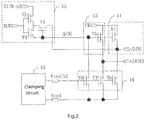
- FIG. 2 is a schematic structural view of the second embodiment of the GOA circuit of the present disclosure
- the GOA circuit includes a pull-up circuit 11, a pull-up control circuit 12, a passing down circuit 13, a first pull-down circuit 14, a clamping circuit 15, a scan output terminal G(N) and a level-transmission output terminal ST(N).
- the pull-up circuit 11 and the pull-up control circuit 12 are connected in the same manner as in the above-described first embodiment, and will not be described here.
- the passing down circuit 13 includes a fifth switch tube T5 having a control terminal coupled to the second connection terminal of the third switch tube T3 and a second connection terminal coupled to the level-transmission output terminal ST(N).
- the level-transmission output terminal ST(N) is similar to the scan output terminal G(N), which also outputs the CK signal when T5 is turned on, but the outputted signal is used to input the next stage or lower n-stage GOA circuit pull-up control circuit.
- the first pull-down circuit 14 includes: a sixth switch tube T6 having a first connection terminal coupled to the scan output terminal G(N).
- a seventh switch tube T7 having a first connection terminal coupled to the level-transmission output terminal ST(N); a eighth switch tube T8 having a first connection terminal coupled to the second output terminal of the third switch tube T3.
- a clamping circuit 15 coupled to the control terminal and second connection terminal of the sixth switch tube T6, the seventh switch tube T7 and the eighth switch tube T8 for controlling the control terminal level of the sixth switch tube T6, the seventh switch tube T7 and the eighth switch tube T8 to be lower than the second connection terminal level of the sixth switch tube T6, the seventh switch tube T7 and the eighth switch tube T8, when the first level is outputted at the scan output terminal G(N) and for controlling the control terminal level of the sixth switch tube T6, the seventh switch tube T7 and the eighth switch tube T8 to be higher than the second connection terminal level of the sixth switch tube T6, the seventh switch tube T7 and the eighth switch tube T8, when the second level is outputted at the scan output terminal, the first level being higher than the second level.
- the clamping circuit 15 supplies Vss2 to the control terminals of T6, T7 and T8, and Vss1 to the second terminals of T6, T7 and T8, where Vss1 > Vss2, and T6, T7 and T8 are completely turned off.
- T6, T7, and T8 are turned on, and the level of G (N) is pulled low by the low level Vss1. Accordingly, the clamping circuit 15 supplies the control terminal of T6, T7, T8 a high level, supplies the Vss1 to the second connection terminal of T6, T7, T8, ensure the T6, T7, T8 are turned on.
- FIG. 3 is a schematic structural view of the third embodiment of the GOA circuit of the present disclosure
- the GOA circuit includes a pull-up circuit 11, a pull-up control circuit 12, a passing down circuit 13, a first pull-down circuit 14, a clamping circuit 15, a second pull-down circuit 16, a scan output terminal G(N) and a level-transmission output terminal ST(N).
- the pull-up circuit 11, the pull-up control circuit 12, the passing down circuit 13, the first pull-down circuit 14, the clamping circuit 15 are connected in the same manner as in the above-described second embodiment, and will not be described here.
- the second pull-down circuit 16 includes: a ninth switch tube T9 having a first connection terminal coupled to the second connection terminal of the third switch tube T3.
- a tenth switch tube T10 having a first connection terminal coupled to the level-transmission output terminal ST(N).
- a eleventh switch tube T11 having a first connection terminal coupled to the scan output terminal G(N).
- the clamping circuit 15 coupled to the control terminal and second connection terminal of the ninth switch tube T9, the tenth switch tube T10, the eleventh switch tube T11 for controlling the control terminal level of the ninth switch tube T9, the tenth switch tube T10, the eleventh switch tube T11 to be lower than the second connection terminal level of the ninth switch tube T9, the tenth switch tube T10, the eleventh switch tube T11, when the scan output terminal outputted the first level, and for controlling the control terminal level of the ninth switch tube T9, the tenth switch tube T10, the eleventh switch tube T11 to be higher than the second connection terminal level of the ninth switch tube T9, the tenth switch tube T10, the eleventh switch tube T11, when the scan output terminal outputted the second level.
- the second pull-down circuit 16 of the present embodiment is the same as the first pull-down circuit 14 and will not be described again.
- the clamping circuit 15 controls the first pull-down circuit 14 and the second pull-down circuit 16 to operate alternately.
- FIG. 4 is a schematic circuit diagram of the fourth embodiment of the GOA circuit of the present disclosure, the GOA circuit includes a pull-up circuit 11, a pull-up control circuit 12, a passing down circuit 13, a first pull-down circuit 14, a clamping circuit 15, a second pull-down circuit 16, a scan output terminal G(N) and a level-transmission output terminal ST(N).
- the pull-up circuit 11, the pull-up control circuit 12, the passing down circuit 13, the first pull-down circuit 14, and the second pull-down circuit 16 are the same as in the above-described embodiment, and will not be described here.
- the clamping circuit 15 includes a first control circuit, a second control circuit, a first clamp terminal, a second clamp terminal.
- the first clamp terminal is connected with the third level Vss1, coupled to the second connection terminal of the sixth switch tube T6, the seventh switch tube 67 and the eighth switch tube 68, the second clamp terminal is connected with the fourth level Vss2, the third level Vss1 is higher than the fourth level Vss2.
- the first control circuit includes: a twelfth switch tube T12 having a control terminal and a first connection terminal connected with a first control signal LC1.
- a thirteenth switch tube T13 having a control terminal coupled to the second connection terminal of the twelfth switch tube T12, a first connection terminal connected with the first control signal LC1, a second connection terminal coupled to the control terminal of the sixth switch tube T6, the seventh switch tube T7 and the eighth switch tube T8.
- a fourteenth switch tube T14 having a control terminal coupled to the second connection terminal of the third switch tube T3, a first connection terminal coupled to the second connection terminal of the twelfth switch tube T12, a second connection terminal coupled to the second clamp terminal.
- a fifteenth switch tube T15 having a control terminal coupled to the second connection terminal of the third switch tube T3, a first connection terminal coupled to the second connection terminal of the thirteenth switch tube T13, a second connection terminal coupled to the second clamp terminal.
- control terminal level of the sixth switch tube T6, the seventh switch tube T7, and the eighth switch tube T8 is defined as P(N).
- the second control circuit includes: a sixteenth switch tube T16 having a control terminal and a first connection terminal connected with the second control signal LC2.
- a seventeenth switch tube T17 having a control terminal coupled to the second connection terminal of the sixteenth switch tube, a first connection terminal connected with a second control signal LC2, a second connection tube coupled to the control terminal of the ninth switch tube T9, the tenth switch tube T10 and the eleventh switch tube T11.
- An eighteenth switch tube T18 having a control terminal coupled to the second connection terminal of the third switch tube T3, a first connection terminal coupled to the second connection terminal of the sixteenth switch tube T16, a second connection terminal coupled to the second clamp terminal.
- a nineteenth switch tube T19 having a control terminal coupled to the second connection terminal of the third switch tube T3, a first connection terminal coupled to the second connection terminal of the seventeenth switch tube T17, a second connection terminal coupled to the second clamp terminal.
- control terminal level of the ninth switch tube T9, the tenth switch tube T10, and the eleventh switch tube T11 is defined as K (N).
- the pull-up circuit 11 further includes a capacitor Cb coupled between the scan output terminal G (N) and the control terminal of the first switch tube T1.
- the first connection terminal of the first switch tube T1 is connected with the first clock signal CK
- the control terminal of the second switch tube T2 and the third switch tube T3 are connected with the second clock signal XCK
- the first connection terminal of the second switch tube T2 is connected with the level-transmission signal ST(N-4); the first clock signal CK is opposite to the second clock signal XCK.
- the present embodiment uses eight clock signals CK, that is, the CK signal of the Nth GOA circuit is the same as the CK signal of the (N + 8) th GOA circuit and opposite to the CK signal of the (N + 4) th GOA circuit.
- LC1, LC2 is the opposite of a set of low-frequency AC power supply, 100 frame reversal time.
- Vss1, Vss2 are two DC power supplies, Vss1> Vss2.
- CK4 is high, the low level of ST(28) is to Q(32), the Q(32) is pulled low; at the same time, K(32) is low level, P(32) is high level, T6, T7, T8 are opened, Q(32), G(32), ST(32) are pulled low.
- the first and second connection terminals of the above-described switch tube do not represent the order of the pin of the switch tube but rather the specific designation of the pin of the switch pin.
- the switch tube mentioned in each of the above embodiments is a TFT (Thin Film Transistor) fabricated by IGZO, alternatively, the TFT in the above-described embodiment is N-type, the control terminal is a gate, the first connection terminal is a source and the second connection terminal is a drain; or the control terminal is a gate, the first connection terminal is a drain and the second connection terminal is a source.
- TFT Thin Film Transistor
- a P-type TFT may be used for connection of the circuits, and it is only necessary to adjust the control terminal level or the order of the source and drain electrodes in accordance with the above-described embodiment.
- FIG. 7 is a schematic structural view of an embodiment of the liquid crystal display of the present disclosure
- the liquid crystal display includes the display panel 71 and the driving circuit 72, wherein, the driving circuit 72 is arranged at the side of the display panel 71, is used to drive the display panel 71.
- the driving circuit 72 is a GOA circuit as described in each of the above embodiments, and operates similarly to the circuit configuration, and will not be described again.
Landscapes
- Engineering & Computer Science (AREA)
- Chemical & Material Sciences (AREA)
- Crystallography & Structural Chemistry (AREA)
- Physics & Mathematics (AREA)
- Computer Hardware Design (AREA)
- General Physics & Mathematics (AREA)
- Theoretical Computer Science (AREA)
- Control Of Indicators Other Than Cathode Ray Tubes (AREA)
- Liquid Crystal Display Device Control (AREA)
- Liquid Crystal (AREA)
Abstract
Description
- The present disclosure relates to liquid crystal display technologies, and more particularly to a gate driver on array (GOA) circuit and a liquid crystal display.
- Gate driver on array (GOA) technologies have been widely used and research because they advantage display products to have a narrow frame or be borderless, and reduce a binding process of an external integrated circuit (IC) to enhance productivity and reduce product costs.
- Indium gallium zinc oxide (IGZO) has been widely used in a production of GOA circuits to reduce the complexity of the GOA circuits because of its high mobility and good device stability. In detail, the IGZO has advantage over production of a narrow frame display because of its high mobility for producing a thin film transistor with a smaller size relative to a size of a thin film transistor fabricated by amorphous silicon (a-Si) in the process of manufacturing thin film transistors in the GOA circuits. Meanwhile, due to good device stability, the IGZO can use for producing a relatively simple GOA circuit and reduce power consumption by means of reduced numbers of power and thin-film transistor used for stabilizing performance of the thin-film transistor.
- However, a threshold voltage Vth of the thin-film transistor manufactured by the IGZO is liable to be a negative value, resulting in a failure of the GOA circuit.
- The present disclosure solves the above-mentioned problems and provides a gate driver on array (GOA) circuit and a liquid crystal display device preventing from erroneously turning on or off of a transistor and causing a problem of circuit output error due to drift of threshold value.
- In order to solve the above technical problem, the disclosure adopts the technical scheme is: provides a GOA circuit, the GOA circuit includes: a pull-up circuit including a first switch tube, a scan output terminal coupled to a second connection terminal of the first switch tube, a pull-up control circuit including: a second switch tube; a third switch tube having a first connection terminal coupled to the second connection terminal of the second switch tube and a second connection terminal coupled to the control terminal of the first switch tube; a fourth switch tube having a control terminal coupled to the control terminal of the first switch tube, a first connection terminal coupled to the first connection terminal of the third switch tube and a second connection terminal coupled to the scan output terminal for controlling the control terminal level of the second switch tube to be lower than the first connection terminal level of the second switch tube when the first level is outputted at the scan output terminal.
- Wherein, the GOA circuit further includes: a passing down circuit including a fifth switch tube whose control terminal is coupled to the second connection terminal of the third switch tube and whose second connection terminal is coupled to the level-transmission output terminal.
- Wherein, the GOA circuit further includes a pull-down circuit and a clamping circuit; the first pull-down circuit includes: a sixth switch tube having a first connection terminal coupled to the scan output terminal; a seventh switch tube having a first connection terminal coupled to the level-transmission output terminal; a eighth switch tube having a first connection terminal coupled to the second connection terminal of the third switch tube; the clamping circuit is coupled to the control terminal and second connection terminal of the sixth switch tube, the seventh switch tube and the eighth switch tube for controlling the control terminal level of the sixth switch tube, the seventh switch tube and the eighth switch tube to be lower than the second connection terminal level of the sixth switch tube, the seventh switch tube and the eighth switch tube, when the first level is outputted at the scan output terminal and for controlling the control terminal level of the sixth switch tube, the seventh switch tube and the eighth switch tube to be higher than the second connection terminal level of the sixth switch tube, the seventh switch tube and the eighth switch tube, when the second level is outputted at the scan output terminal, the first level being higher than the second level.
wherein, the GOA circuit further includes a second pull-down circuit; the second pull-down circuit includes: a ninth switch tube having the first connection terminal coupled to the second connection terminal of the third switch tube; a tenth switch tube having the first connection terminal coupled to the level-transmission output terminal; a eleventh switch tube having the first connection terminal coupled to the scan output terminal; the clamping circuit coupled to the control terminal and second connection terminal of the ninth switch tube, the tenth switch tube, the eleventh switch tube for controlling the control terminal level of the ninth switch tube, the tenth switch tube, the eleventh switch tube to be lower than the second connection terminal level of the ninth switch tube, the tenth switch tube, the eleventh switch tube, when the scan output terminal outputted the first level, and for controlling the control terminal level of the ninth switch tube, the tenth switch tube, the eleventh switch tube to be higher than the second connection terminal level of the ninth switch tube, the tenth switch tube, the eleventh switch tube, when the scan output terminal outputted the second level. - Wherein, the clamping circuit controls the first pull-down circuit and the second pull-down circuit to operate alternately.
- Wherein, the clamping circuit includes a first control circuit, a first clamp terminal and a second clamp terminal; the first clamp terminal is connected with a third level and is coupled to the second connection terminal of the sixth switch tube, the seventh switch tube and the eighth switch tube, the second clamp terminal is connected with a fourth level, the third level is higher than the fourth level; the first control circuit includes: a twelfth switch tube having a control terminal and a first connection terminal connected with a first control signal; a thirteen switch tube having a control terminal coupled to the second connection terminal of the twelfth switch tube, a first connection terminal connected with the first control signal, a second connection terminal coupled to the control terminal of the sixth switch tube, the seventh switch tube and the eighth switch tube; a fourteenth switch tube having a control terminal coupled to the second connection terminal of the third switch tube, a first connection terminal coupled to the second connection terminal of the twelfth switch tube, a second connection terminal coupled to the second clamp terminal; a fifteenth switch tube having a control terminal coupled to the second connection terminal of the third switch tube, a first connection terminal coupled to the second connection terminal of the thirteenth switch tube, a second connection terminal coupled to the second clamp terminal.
- Wherein, the clamping circuit further includes a second control circuit; the second control circuit includes: a sixteenth switch tube having a control terminal and a first connection terminal connected with a second control signal; a seventeenth switch tube having a control terminal coupled to the second connection terminal of the sixteenth switch tube, a first connection terminal connected with the second control signal, a second connection terminal coupled to the control terminal of the ninth switch tube, the tenth switch tube and the eleventh switch tube; a eighteenth switch tube having a control terminal coupled to the second connection terminal of the third switch tube, a first connection terminal coupled to the second connection terminal of the sixteenth switch tube, a second connection terminal coupled to the second clamp terminal; a nineteenth switch tube having a control terminal coupled to the second connection terminal of the third switch tube, a first connection terminal coupled to the second connection terminal of the seventeenth switch tube, a second connection terminal coupled to the second clamp terminal.
- Wherein, the pull-up circuit further includes a capacitor coupled between the scan output terminal and the control terminal of the first switch tube.
- Wherein, the first connection terminal of the first switch tube is connected with a first clock signal, the control terminal of the second switch tube and the third switch tube is connected with a second clock signal, the first connection terminal of the second switch tube is connected with a level-transmission signal; and the first clock signal is opposite to the second clock signal.
- In order to solve the above-mentioned technical problems, another technical scheme adopted by the present disclosure is: provides a liquid crystal display, the liquid crystal display includes a GOA circuit, the GOA circuit includes: a pull-up circuit including a first switch tube; a scan output terminal coupled to the second connection terminal of the first switch tube; the pull-up circuit further includes a capacitor coupled between the scan output terminal and the control terminal of the first switch tube; a pull-up control circuit including: a second switch tube; a third switch tube having a first connection terminal coupled to the second connection terminal of the second switch tube and a second connection terminal coupled to the control terminal of the first switch tube; a fourth switch tube having a control terminal coupled to the control terminal of the first switch tube, a first connection terminal coupled to the first connection terminal of the third switch tube and a second connection terminal coupled to the scan output terminal for controlling the control terminal level of the second switch tube to be lower than the first connection terminal level of the second switch tube when the first level is outputted at the scan output terminal; wherein, the first connection terminal of the first switch tube is connected with a first clock signal, the control terminal of the second switch tube and the third switch tube is connected with a second clock signal, the first connection terminal of the second switch tube is connected with a level-transmission signal, and the first clock signal is opposite to the second clock signal.
wherein, the GOA circuit further includes: a passing down circuit including a fifth switch tube whose control terminal is coupled to the second connection terminal of the third switch tube and whose second connection terminal is coupled to the level-transmission output terminal. - Wherein, the GOA circuit further includes a pull-down circuit and a clamping circuit; the first pull-down circuit includes: a sixth switch tube having a first connection terminal coupled to the scan output terminal; a seventh switch tube having a first connection terminal coupled to the level-transmission output terminal; a eighth switch tube having a first connection terminal coupled to the second connection terminal of the third switch tube; the clamping circuit is coupled to the control terminal and second connection terminal of the sixth switch tube, the seventh switch tube and the eighth switch tube for controlling the control terminal level of the sixth switch tube, the seventh switch tube and the eighth switch tube to be lower than the second connection terminal level of the sixth switch tube, the seventh switch tube and the eighth switch tube, when the first level is outputted at the scan output terminal and for controlling the control terminal level of the sixth switch tube, the seventh switch tube and the eighth switch tube to be higher than the second connection terminal level of the sixth switch tube, the seventh switch tube and the eighth switch tube, when the second level is outputted at the scan output terminal, the first level being higher than the second level.
wherein, the GOA circuit further includes a second pull-down circuit; the second pull-down circuit includes: a ninth switch tube having the first connection terminal coupled to the second connection terminal of the third switch tube; a tenth switch tube having the first connection terminal coupled to the level-transmission output terminal; a eleventh switch tube having the first connection terminal coupled to the scan output terminal; the clamping circuit coupled to the control terminal and second connection terminal of the ninth switch tube, the tenth switch tube, the eleventh switch tube for controlling the control terminal level of the ninth switch tube, the tenth switch tube, the eleventh switch tube to be lower than the second connection terminal level of the ninth switch tube, the tenth switch tube, the eleventh switch tube, when the scan output terminal outputted the first level, and for controlling the control terminal level of the ninth switch tube, the tenth switch tube, the eleventh switch tube to be higher than the second connection terminal level of the ninth switch tube, the tenth switch tube, the eleventh switch tube, when the scan output terminal outputted the second level. - Wherein, the clamping circuit controls the first pull-down circuit and the second pull-down circuit to operate alternately.
- Wherein, the clamping circuit includes a first control circuit, a first clamp terminal and a second clamp terminal; the first clamp terminal is connected with a third level and is coupled to the second connection terminal of the sixth switch tube, the seventh switch tube and the eighth switch tube, the second clamp terminal is connected with a fourth level, the third level is higher than the fourth level; the first control circuit includes: a twelfth switch tube having a control terminal and a first connection terminal connected with a first control signal; a thirteen switch tube having a control terminal coupled to the second connection terminal of the twelfth switch tube, a first connection terminal connected with the first control signal, a second connection terminal coupled to the control terminal of the sixth switch tube, the seventh switch tube and the eighth switch tube; a fourteenth switch tube having a control terminal coupled to the second connection terminal of the third switch tube, a first connection terminal coupled to the second connection terminal of the twelfth switch tube, a second connection terminal coupled to the second clamp terminal; a fifteenth switch tube having a control terminal coupled to the second connection terminal of the third switch tube, a first connection terminal coupled to the second connection terminal of the thirteenth switch tube, a second connection terminal coupled to the second clamp terminal.
- Wherein, the clamping circuit further includes a second control circuit; the second control circuit includes: a sixteenth switch tube having a control terminal and a first connection terminal connected with a second control signal; a seventeenth switch tube having a control terminal coupled to the second connection terminal of the sixteenth switch tube, a first connection terminal connected with the second control signal, a second connection terminal coupled to the control terminal of the ninth switch tube, the tenth switch tube and the eleventh switch tube; a eighteenth switch tube having a control terminal coupled to the second connection terminal of the third switch tube, a first connection terminal coupled to the second connection terminal of the sixteenth switch tube, a second connection terminal coupled to the second clamp terminal; a nineteenth switch tube having a control terminal coupled to the second connection terminal of the third switch tube, a first connection terminal coupled to the second connection terminal of the seventeenth switch tube, a second connection terminal coupled to the second clamp terminal.
- In order to solve the above-mentioned technical problems, the other technical scheme adopted by the present disclosure is: provides a liquid crystal display, the liquid crystal display includes a GOA circuit, the GOA circuit includes: a pull-up circuit including a first switch tube; a scan output terminal coupled to the second connection terminal of the first switch tube; a pull-up control circuit including: a second switch tube; a third switch tube having a first connection terminal coupled to the second connection terminal of the second switch tube and a second connection terminal coupled to the control terminal of the first switch tube; a fourth switch tube having a control terminal coupled to the control terminal of the first switch tube, a first connection terminal coupled to the first connection terminal of the third switch tube and a second connection terminal coupled to the scan output terminal for controlling the control terminal level of the second switch tube to be lower than the first connection terminal level of the second switch tube when the first level is outputted at the scan output terminal.
- Wherein, the GOA circuit further includes: a passing down circuit including a fifth switch tube whose control terminal is coupled to the second connection terminal of the third switch tube and whose second connection terminal is coupled to the level-transmission output terminal.
- Wherein, the GOA circuit further includes a pull-down circuit and a clamping circuit; the first pull-down circuit includes: a sixth switch tube having a first connection terminal coupled to the scan output terminal; a seventh switch tube having a first connection terminal coupled to the level-transmission output terminal; a eighth switch tube having a first connection terminal coupled to the second connection terminal of the third switch tube; the clamping circuit is coupled to the control terminal and second connection terminal of the sixth switch tube, the seventh switch tube and the eighth switch tube for controlling the control terminal level of the sixth switch tube, the seventh switch tube and the eighth switch tube to be lower than the second connection terminal level of the sixth switch tube, the seventh switch tube and the eighth switch tube, when the first level is outputted at the scan output terminal and for controlling the control terminal level of the sixth switch tube, the seventh switch tube and the eighth switch tube to be higher than the second connection terminal level of the sixth switch tube, the seventh switch tube and the eighth switch tube, when the second level is outputted at the scan output terminal, the first level being higher than the second level.
wherein, the GOA circuit further includes a second pull-down circuit; the second pull-down circuit includes: a ninth switch tube having the first connection terminal coupled to the second connection terminal of the third switch tube; a tenth switch tube having the first connection terminal coupled to the level-transmission output terminal; a eleventh switch tube having the first connection terminal coupled to the scan output terminal; the clamping circuit coupled to the control terminal and second connection terminal of the ninth switch tube, the tenth switch tube, the eleventh switch tube for controlling the control terminal level of the ninth switch tube, the tenth switch tube, the eleventh switch tube to be lower than the second connection terminal level of the ninth switch tube, the tenth switch tube, the eleventh switch tube, when the scan output terminal outputted the first level, and for controlling the control terminal level of the ninth switch tube, the tenth switch tube, the eleventh switch tube to be higher than the second connection terminal level of the ninth switch tube, the tenth switch tube, the eleventh switch tube, when the scan output terminal outputted the second level. - The present disclosure has the advantages is: different from the state of the prior art, the GOA circuit of the present disclosure includes: a pull-up circuit including a first switch tube; a scan output terminal coupled to the second connection terminal of the first switch tube; a pull-up control circuit including: a second switch tube; a third switch tube having a first connection terminal coupled to the second connection terminal of the second switch tube and a second connection terminal coupled to the control terminal of the first switch tube; a fourth switch tube having a control terminal coupled to the control terminal of the first switch tube, a first connection terminal coupled to the first connection terminal of the third switch tube and a second connection terminal coupled to the scan output terminal. In this way, the level of the first connection terminal of the third switch tube can be raised in the scanning phase by the action of the fourth switch tube so that the control terminal level of the third switch tube is smaller than the first connection terminal level, avoid the third switch tube threshold drift error affect the output of the scan terminal.
-
-
Figure 1 is a schematic structural view of the first embodiment of the GOA circuit of the present disclosure; -
Figure 2 is a schematic structural view of the second embodiment of the GOA circuit of the present disclosure; -
Figure 3 is a schematic structural view of the third embodiment of the GOA circuit of the present disclosure; -
Figure 4 is a schematic circuit diagram of the fourth embodiment of the GOA circuit of the present disclosure; -
Figure 5 is a schematic diagram of the clock signal of the fourth embodiment of the GOA circuit of the present disclosure; -
Figure 6 is a schematic diagram of the output signal of the fourth embodiment of the GOA circuit of the present disclosure; -
Figure 7 is a schematic structural view of an embodiment of the liquid crystal display of the present disclosure. - Referring to
FIG. 1, FIG. 1 is a schematic structural view of the first embodiment of the GOA circuit of the present disclosure, the GOA circuit includes:
a pull-up circuit 11 including a first switch tube T1. - A scan output terminal G(N) coupled to the second connection terminal of the first switch tube T1.
- Wherein, the first connection terminal of the first switch tube T1 is connected with the first clock signal CK, when the control terminal of the first switch tube is at the high level, the first switch tube T1 is turned on and the first clock signal CK is outputted through the scan output terminal G (N).
- A pull-
up control circuit 12 includes:
a second switch tube T2. - A third switch tube T3 having a first connection terminal coupled to the second connection terminal of the second switch tube T2, a second connection terminal coupled to the control terminal of the first switch tube T1.
- A fourth switch tube T4 having a control terminal coupled to the control terminal of the first switch tube T1, a first connection terminal coupled to the first connection terminal of the third switch tube T3, a second connection terminal coupled to the scan output terminal G(N) for controlling the control terminal level of the second switch tube T2 to be lower than the first connection terminal level of the second switch tube T1 when the first level is outputted at the scan output terminal.
- Wherein, the first connection terminal of the second switch tube T2 is connected with the level-transmission signal ST(N-n) outputted by the GOA circuit on the upper stage (or upper n stage), the control terminal of the second switch tube T2 and third switch tube T3 are connected with the second clock signal XCK.
- It is understood that the XCK is high level during the scanning preparation stage of the GOA circuit of the stage (i.e., the previous stage of the scanning phase), the stage signal ST (N-n) outputted from the GOA circuit of the upper stage is high level, and the CK is low level.
- In detail, at the high level of XCK, T2 and T3 turn on and the high-level ST (N-n) charge the Q (N) to raise the level of Q (N). In Q (N) under the action of high, the T1 is turned on, but this time the CK is low, so the G (N) output low.
- In the scanning phase, the XCK is low, the CK is high.
- In detail, at the XCK low level, T2 and T3 are turned off, the Q (N) continue to maintain high. In the Q (N) under the action of high, the T1 continues to turn on, this time CK is high, so G (N) output high.
- It should be noted that at this stage, T4 turns on and the high level of G (N) goes to the first connection terminal of T3 under the effect of Q (N) high, so that the first connection terminal of T3 level T3 higher than the control side, to prevent the T3 at this stage threshold drift and conduction.
- Different from the prior art, the GOA circuit of the present disclosure includes: a pull-up circuit including a first switch tube; a scan output terminal coupled to the second connection terminal of the first switch tube; a pull-up control circuit including: a second switch tube; a third switch tube having a first connection terminal coupled to the second connection terminal of the second switch tube and a second connection terminal coupled to the control terminal of the first switch tube; a fourth switch tube having a control terminal coupled to the control terminal of the first switch tube, a first connection terminal coupled to the first connection terminal of the third switch tube and a second connection terminal coupled to the scan output terminal. In this way, the level of the first connection terminal of the third switch tube can be raised in the scanning phase by the action of the fourth switch tube so that the control terminal level of the third switch tube is smaller than the first connection terminal level, avoid the third switch tube threshold drift error affect the output of the scan terminal.
- Referring to
FIG. 2, FIG. 2 is a schematic structural view of the second embodiment of the GOA circuit of the present disclosure, the GOA circuit includes a pull-up circuit 11, a pull-up control circuit 12, a passing downcircuit 13, a first pull-down circuit 14, aclamping circuit 15, a scan output terminal G(N) and a level-transmission output terminal ST(N). - Wherein, the pull-
up circuit 11 and the pull-up control circuit 12 are connected in the same manner as in the above-described first embodiment, and will not be described here. - The passing down
circuit 13 includes a fifth switch tube T5 having a control terminal coupled to the second connection terminal of the third switch tube T3 and a second connection terminal coupled to the level-transmission output terminal ST(N). - Wherein, the level-transmission output terminal ST(N) is similar to the scan output terminal G(N), which also outputs the CK signal when T5 is turned on, but the outputted signal is used to input the next stage or lower n-stage GOA circuit pull-up control circuit.
- Wherein, the first pull-
down circuit 14 includes:
a sixth switch tube T6 having a first connection terminal coupled to the scan output terminal G(N). - A seventh switch tube T7 having a first connection terminal coupled to the level-transmission output terminal ST(N);
a eighth switch tube T8 having a first connection terminal coupled to the second output terminal of the third switch tube T3. - A clamping
circuit 15 coupled to the control terminal and second connection terminal of the sixth switch tube T6, the seventh switch tube T7 and the eighth switch tube T8 for controlling the control terminal level of the sixth switch tube T6, the seventh switch tube T7 and the eighth switch tube T8 to be lower than the second connection terminal level of the sixth switch tube T6, the seventh switch tube T7 and the eighth switch tube T8, when the first level is outputted at the scan output terminal G(N) and for controlling the control terminal level of the sixth switch tube T6, the seventh switch tube T7 and the eighth switch tube T8 to be higher than the second connection terminal level of the sixth switch tube T6, the seventh switch tube T7 and the eighth switch tube T8, when the second level is outputted at the scan output terminal, the first level being higher than the second level. - It is understood that, in the G (N) output high, T1, T5 open, Q (N) is high; At this time, should ensure that T6, T7, T8 completely cut-off, in order to prevent the conduction threshold drift of T6, T7, T8, the clamping
circuit 15 supplies Vss2 to the control terminals of T6, T7 and T8, and Vss1 to the second terminals of T6, T7 and T8, where Vss1 > Vss2, and T6, T7 and T8 are completely turned off. - When G (N) outputs a low level, T6, T7, and T8 are turned on, and the level of G (N) is pulled low by the low level Vss1. Accordingly, the clamping
circuit 15 supplies the control terminal of T6, T7, T8 a high level, supplies the Vss1 to the second connection terminal of T6, T7, T8, ensure the T6, T7, T8 are turned on. - Referring to
FIG. 3, FIG. 3 is a schematic structural view of the third embodiment of the GOA circuit of the present disclosure, the GOA circuit includes a pull-upcircuit 11, a pull-upcontrol circuit 12, a passing downcircuit 13, a first pull-down circuit 14, a clampingcircuit 15, a second pull-down circuit 16, a scan output terminal G(N) and a level-transmission output terminal ST(N). - Wherein, the pull-up
circuit 11, the pull-upcontrol circuit 12, the passing downcircuit 13, the first pull-down circuit 14, the clampingcircuit 15 are connected in the same manner as in the above-described second embodiment, and will not be described here. - Wherein, the second pull-
down circuit 16 includes:
a ninth switch tube T9 having a first connection terminal coupled to the second connection terminal of the third switch tube T3. - A tenth switch tube T10 having a first connection terminal coupled to the level-transmission output terminal ST(N).
- A eleventh switch tube T11 having a first connection terminal coupled to the scan output terminal G(N).
the clampingcircuit 15 coupled to the control terminal and second connection terminal of the ninth switch tube T9, the tenth switch tube T10, the eleventh switch tube T11 for controlling the control terminal level of the ninth switch tube T9, the tenth switch tube T10, the eleventh switch tube T11 to be lower than the second connection terminal level of the ninth switch tube T9, the tenth switch tube T10, the eleventh switch tube T11, when the scan output terminal outputted the first level, and for controlling the control terminal level of the ninth switch tube T9, the tenth switch tube T10, the eleventh switch tube T11 to be higher than the second connection terminal level of the ninth switch tube T9, the tenth switch tube T10, the eleventh switch tube T11, when the scan output terminal outputted the second level. - It will be understood that the second pull-
down circuit 16 of the present embodiment is the same as the first pull-down circuit 14 and will not be described again. - Alternatively, in the present embodiment, the clamping
circuit 15 controls the first pull-down circuit 14 and the second pull-down circuit 16 to operate alternately. - Referring to
FIG. 4, FIG. 4 is a schematic circuit diagram of the fourth embodiment of the GOA circuit of the present disclosure, the GOA circuit includes a pull-upcircuit 11, a pull-upcontrol circuit 12, a passing downcircuit 13, a first pull-down circuit 14, a clampingcircuit 15, a second pull-down circuit 16, a scan output terminal G(N) and a level-transmission output terminal ST(N). - Wherein, the pull-up
circuit 11, the pull-upcontrol circuit 12, the passing downcircuit 13, the first pull-down circuit 14, and the second pull-down circuit 16 are the same as in the above-described embodiment, and will not be described here. - Wherein, the clamping
circuit 15 includes a first control circuit, a second control circuit, a first clamp terminal, a second clamp terminal. - The first clamp terminal is connected with the third level Vss1, coupled to the second connection terminal of the sixth switch tube T6, the seventh switch tube 67 and the eighth switch tube 68, the second clamp terminal is connected with the fourth level Vss2, the third level Vss1 is higher than the fourth level Vss2.
- The first control circuit includes:
a twelfth switch tube T12 having a control terminal and a first connection terminal connected with a first control signal LC1. - A thirteenth switch tube T13 having a control terminal coupled to the second connection terminal of the twelfth switch tube T12, a first connection terminal connected with the first control signal LC1, a second connection terminal coupled to the control terminal of the sixth switch tube T6, the seventh switch tube T7 and the eighth switch tube T8.
- A fourteenth switch tube T14 having a control terminal coupled to the second connection terminal of the third switch tube T3, a first connection terminal coupled to the second connection terminal of the twelfth switch tube T12, a second connection terminal coupled to the second clamp terminal.
- A fifteenth switch tube T15 having a control terminal coupled to the second connection terminal of the third switch tube T3, a first connection terminal coupled to the second connection terminal of the thirteenth switch tube T13, a second connection terminal coupled to the second clamp terminal.
- Wherein, the control terminal level of the sixth switch tube T6, the seventh switch tube T7, and the eighth switch tube T8 is defined as P(N).
- The second control circuit includes:
a sixteenth switch tube T16 having a control terminal and a first connection terminal connected with the second control signal LC2. - A seventeenth switch tube T17 having a control terminal coupled to the second connection terminal of the sixteenth switch tube, a first connection terminal connected with a second control signal LC2, a second connection tube coupled to the control terminal of the ninth switch tube T9, the tenth switch tube T10 and the eleventh switch tube T11.
- An eighteenth switch tube T18 having a control terminal coupled to the second connection terminal of the third switch tube T3, a first connection terminal coupled to the second connection terminal of the sixteenth switch tube T16, a second connection terminal coupled to the second clamp terminal.
- A nineteenth switch tube T19 having a control terminal coupled to the second connection terminal of the third switch tube T3, a first connection terminal coupled to the second connection terminal of the seventeenth switch tube T17, a second connection terminal coupled to the second clamp terminal.
- Wherein, the control terminal level of the ninth switch tube T9, the tenth switch tube T10, and the eleventh switch tube T11 is defined as K (N).
- Optionally, the pull-up
circuit 11 further includes a capacitor Cb coupled between the scan output terminal G (N) and the control terminal of the first switch tube T1. - Alternatively, the present embodiment will be described below with reference to a specific embodiment:
- In the present embodiment, the first connection terminal of the first switch tube T1 is connected with the first clock signal CK, the control terminal of the second switch tube T2 and the third switch tube T3 are connected with the second clock signal XCK, the first connection terminal of the second switch tube T2 is connected with the level-transmission signal ST(N-4); the first clock signal CK is opposite to the second clock signal XCK.
- In particular, as shown in
FIG. 5 . The present embodiment uses eight clock signals CK, that is, the CK signal of the Nth GOA circuit is the same as the CK signal of the (N + 8) th GOA circuit and opposite to the CK signal of the (N + 4) th GOA circuit. LC1, LC2 is the opposite of a set of low-frequency AC power supply, 100 frame reversal time. Vss1, Vss2 are two DC power supplies, Vss1> Vss2. - With the above-mentioned waveform into the circuit, the following in conjunction with
FIG. 6 , with the 32th GOA (G32) as an example to illustrate the circuit operation. - Assume that LC1 is high level H and LC2 is low level L in this frame.
- When G (N) = G (32), ST (N-4) = ST (28), G (32) is controlled by CK8, ST (28) is controlled by CK4 and XCK is CK4.
- When ST (28) is high, CK4 is high level, T2, T3 open, the high level of ST (28) to Q (32), Q is high level. At the same time, T1, T5 open, this time, CK8 is low, so G (32), ST (32) is low; at the same time, since Q is high, T14, T15, T18, T19 open, Vss2 makes P (32), K (32) are low, T6, T7, T8, T9, T10, T11 are off, at this time, the control terminal of T6, T7, T8, T9, T10, T11 is Vss2, the second connection end is Vss1, Vss1 is greater than Vss2, therefore, T6, T7, T8, T9, T10, T11 will not turn on erroneously due to the conduction threshold drift and will not affect the level of G (N).
- Then, ST (28) is low, CK4 is low, T2, T3 closed, this time, CK8 is high, G (32) output high, Q (32) by the coupling effect of capacitance Cb, is raised to a higher level; P (32), K (32) continue to remain low.
- Then, CK4 is high, the low level of ST(28) is to Q(32), the Q(32) is pulled low; at the same time, K(32) is low level, P(32) is high level, T6, T7, T8 are opened, Q(32), G(32), ST(32) are pulled low.
- It will be appreciated, by those skilled in the art that the first and second connection terminals of the above-described switch tube do not represent the order of the pin of the switch tube but rather the specific designation of the pin of the switch pin. The switch tube mentioned in each of the above embodiments is a TFT (Thin Film Transistor) fabricated by IGZO, alternatively, the TFT in the above-described embodiment is N-type, the control terminal is a gate, the first connection terminal is a source and the second connection terminal is a drain; or the control terminal is a gate, the first connection terminal is a drain and the second connection terminal is a source.
- In other embodiments, a P-type TFT may be used for connection of the circuits, and it is only necessary to adjust the control terminal level or the order of the source and drain electrodes in accordance with the above-described embodiment.
- Referring to
FIG. 7, FIG. 7 is a schematic structural view of an embodiment of the liquid crystal display of the present disclosure, the liquid crystal display includes thedisplay panel 71 and the drivingcircuit 72, wherein, the drivingcircuit 72 is arranged at the side of thedisplay panel 71, is used to drive thedisplay panel 71. - In detail, the driving
circuit 72 is a GOA circuit as described in each of the above embodiments, and operates similarly to the circuit configuration, and will not be described again. - The above are only embodiments of the present disclosure is not patented and therefore limit the scope of the present disclosure, the use of any content of the present specification and drawings made equivalent or equivalent structural transformation process, either directly or indirectly in other relevant technical fields are included in the same way the scope of patent protection of the present disclosure.
Claims (20)
- A liquid crystal display comprising a gate driver on array, GOA, circuit, characterized in that the GOA circuit comprises:a pull-up circuit comprising a first switch tube;a scan output terminal coupled to a second connection terminal of the first switch tube, wherein the pull-up circuit further comprises a capacitor coupled between the scan output terminal and a control terminal of the first switch tube; anda pull-up control circuit comprising:a second switch tube;a third switch tube comprising a first connection terminal coupled to a second connection terminal of the second switch tube, and a second connection terminal coupled to the control terminal of the first switch tube; anda fourth switch tube comprising:a control terminal coupled to the control terminal of the first switch tube;a first connection terminal coupled to the first connection terminal of the third switch tube; anda second connection terminal coupled to the scan output terminal for controlling a control terminal level of the second switch tube to be lower than a first connection terminal level of the second switch tube when an output at the scan output terminal is a first level, whereina first connection terminal of the first switch tube is connected with a first clock signal;a control terminal of the second switch tube and a control terminal of the third switch tube are connected with a second clock signal;a first connection terminal of the second switch tube is connected with a level-transmission signal; andthe first clock signal is opposite to the second clock signal.
- The liquid crystal display according to claim 1, characterized in that the GOA circuit further comprises:
a passing down circuit comprising a fifth switch tube, wherein a control terminal of the fifth switch tube is coupled to the second connection terminal of the third switch tube, and a second connection terminal of the fifth switch tube is coupled to a level-transmission output terminal. - The liquid crystal display according to claim 2, characterized in that the GOA circuit further comprises a first pull-down circuit and a clamping circuit, wherein the first pull-down circuit comprises:a sixth switch tube comprising a first connection terminal coupled to the scan output terminal;a seventh switch tube comprising a first connection terminal coupled to the level-transmission output terminal; andan eighth switch tube comprising a first connection terminal coupled to the second connection terminal of the third switch tube, wherein the clamping circuit is coupled to a control terminal and a second connection terminal of the sixth switch tube, a control terminal and a second connection terminal of the seventh switch tube, and a control terminal and a second connection terminal of the eighth switch tube forcontrolling a control terminal level of the sixth switch tube, a control terminal level of the seventh switch tube, and a control terminal level of the eighth switch tube to be lower than a second connection terminal level of the sixth switch tube, a second connection terminal level of the seventh switch tube, and a second connection terminal level of the eighth switch tube when an output of the scan output terminal is the first level; and forcontrolling the control terminal level of the sixth switch tube, the control terminal level of the seventh switch tube, and the control terminal level of the eighth switch tube to be higher than the second connection terminal level of the sixth switch tube, the second connection terminal level of the seventh switch tube, and the second connection terminal level of the eighth switch tube when the output of the scan output terminal is a second level, wherein the first level is higher than the second level.
- The liquid crystal display according to claim 3, characterized in that the GOA circuit further comprises a second pull-down circuit, whereinthe second pull-down circuit comprises:a ninth switch tube comprising a first connection terminal coupled to the second connection terminal of the third switch tube;a tenth switch tube comprising a first connection terminal coupled to the level-transmission output terminal; andan eleventh switch tube comprising a first connection terminal coupled to the scan output terminal; andthe clamping circuit is coupled to a control terminal and a second connection terminal of the ninth switch tube, a control terminal and a second connection terminal of the tenth switch tube, and a control terminal and a second connection terminal of the eleventh switch tube forcontrolling a control terminal level of the ninth switch tube, a control terminal level of the tenth switch tube, and a control terminal level of the eleventh switch tube to be lower than the second connection terminal level of the ninth switch tube, the second connection terminal level of the tenth switch tube, and the second connection terminal level of the eleventh switch tube, when the output of the scan output terminal is the first level; and forcontrolling the control terminal level of the ninth switch tube, the control terminal level of the tenth switch tube, and the control terminal level of the eleventh switch tube to be higher than the second connection terminal level of the ninth switch tube, the second connection terminal level of the tenth switch tube, and the second connection terminal level of the eleventh switch tube when the output of the scan output terminal the second level.
- The liquid crystal display according to claim 4, characterized in that the clamping circuit controls the first pull-down circuit and the second pull-down circuit to operate alternately.
- The liquid crystal display according to claim 4, characterized in that the clamping circuit comprises a first control circuit, a first clamp terminal and a second clamp terminal, whereinthe first clamp terminal is connected to a third level and is coupled to the second connection terminal of the sixth switch tube, the second connection terminal of the seventh switch tube and the second connection terminal of the eighth switch tube;the second clamp terminal is connected to a fourth level, wherein the third level is higher than the fourth level; andthe first control circuit comprises:a twelfth switch tube comprising a control terminal and a first connection terminal connected with a first control signal;a thirteenth switch tube comprising a control terminal coupled to a second connection terminal of the twelfth switch tube, a first connection terminal connected to the first control signal, and a second connection terminal coupled to the control terminal of the sixth switch tube, the control terminal of the seventh switch tube, and the control terminal of the eighth switch tube;a fourteenth switch tube comprising a control terminal coupled to the second connection terminal of the third switch tube, a first connection terminal coupled to the second connection terminal of the twelfth switch tube, and a second connection terminal coupled to the second clamp terminal; anda fifteenth switch tube comprising a control terminal coupled to the second connection terminal of the third switch tube, a first connection terminal coupled to the second connection terminal of the thirteenth switch tube, and a second connection terminal coupled to the second clamp terminal.
- The liquid crystal display according to claim 6, characterized in that the clamping circuit further comprises a second control circuit, wherein the second control circuit comprises:a sixteenth switch tube comprising a control terminal and a first connection terminal connected to a second control signal;a seventeenth switch tube comprising a control terminal coupled to a second connection terminal of the sixteenth switch tube, a first connection terminal connected to the second control signal, and a second connection terminal coupled to the control terminal of the ninth switch tube, the control terminal of the tenth switch tube and the control terminal of the eleventh switch tube;an eighteenth switch tube comprising a control terminal coupled to the second connection terminal of the third switch tube, a first connection terminal coupled to the second connection terminal of the sixteenth switch tube, and a second connection terminal coupled to the second clamp terminal; anda nineteenth switch tube comprising a control terminal coupled to the second connection terminal of the third switch tube, a first connection terminal coupled to the second connection terminal of the seventeenth switch tube, and a second connection terminal coupled to the second clamp terminal.
- A GOA circuit, characterized in that the GOA circuit comprises:a pull-up circuit comprising a first switch tube;a scan output terminal coupled to a second connection terminal of the first switch tube; anda pull-up control circuit comprising:a second switch tube;a third switch tube comprising a first connection terminal coupled to a second connection terminal of the second switch tube and a second connection terminal coupled to a control terminal of the first switch tube; anda fourth switch tube comprising a control terminal coupled to the control terminal of the first switch tube, a first connection terminal coupled to the first connection terminal of the third switch tube, and a second connection terminal coupled to the scan output terminal for controlling a control terminal level of the second switch tube to be lower than a first connection terminal level of the second switch tube when an output of the scan output terminal is a first level.
- The GOA circuit according to claim 8, characterized in that the GOA circuit further comprises:
a passing down circuit comprising a fifth switch tube, wherein a control terminal of the fifth switch tube is coupled to the second connection terminal of the third switch tube, and a second connection terminal of the fifth switch tube is coupled to a level-transmission output terminal. - The GOA circuit according to claim 9, characterized in that the GOA circuit further comprises a first pull-down circuit and a clamping circuit, whereinthe first pull-down circuit comprises:a sixth switch tube comprising a first connection terminal coupled to the scan output terminal;a seventh switch tube comprising a first connection terminal coupled to the level-transmission output terminal; andan eighth switch tube comprising a first connection terminal coupled to the second connection terminal of the third switch tube; andthe clamping circuit is coupled to a control terminal and a second connection terminal of the sixth switch tube, a control terminal and a second connection terminal of the seventh switch tube, and a control terminal and a second connection terminal of the eighth switch tube forcontrolling a control terminal level of the sixth switch tube, a control terminal level of the seventh switch tube, and a control terminal level of the eighth switch tube to be lower than a second connection terminal level of the sixth switch tube, a second connection terminal level of the seventh switch tube, and a second connection terminal level of the eighth switch tube when an output of the scan output terminal is the first level; and forcontrolling the control terminal level of the sixth switch tube, the control terminal level of the seventh switch tube, and the control terminal level of the eighth switch tube to be higher than the second connection terminal level of the sixth switch tube, the second connection terminal level of the seventh switch tube, and the second connection terminal level of the eighth switch tube when the output of the scan output terminal is a second level, wherein the first level is higher than the second level.
- The GOA circuit according to claim 10, characterized in that the GOA circuit further comprises a second pull-down circuit, whereinthe second pull-down circuit comprises:a ninth switch tube comprising a first connection terminal coupled to the second connection terminal of the third switch tube;a tenth switch tube comprising a first connection terminal coupled to the level-transmission output terminal; andan eleventh switch tube comprising a first connection terminal coupled to the scan output terminal; andthe clamping circuit is coupled to a control terminal and a second connection terminal of the ninth switch tube, a control terminal and a second connection terminal of the tenth switch tube, and a control terminal and a second connection terminal of the eleventh switch tube forcontrolling a control terminal level of the ninth switch tube, a control terminal level of the tenth switch tube, and a control terminal level of the eleventh switch tube to be lower than a second connection terminal level of the ninth switch tube, a second connection terminal level of the tenth switch tube, and a second connection terminal level of the eleventh switch tube when an output of the scan output terminal is the first level; and forcontrolling the control terminal level of the ninth switch tube, the control terminal level of the tenth switch tube, and the control terminal level of the eleventh switch tube to be higher than the second connection terminal level of the ninth switch tube, the second connection terminal level of the tenth switch tube, and the second connection terminal level of the eleventh switch tube when the output of the scan output terminal is the second level.
- The GOA circuit according to claim 11, characterized in that the clamping circuit controls the first pull-down circuit and the second pull-down circuit to operate alternately.
- The GOA circuit according to claim 11, characterized in that the clamping circuit comprises a first control circuit, a first clamp terminal and a second clamp terminal, whereinthe first clamp terminal is connected to a third level and is coupled to the second connection terminal of the sixth switch tube, the second connection terminal of the seventh switch tube, and the second connection terminal of the eighth switch tube;the second clamp terminal is connected with a fourth level, wherein the third level is higher than the fourth level; andthe first control circuit comprises:a twelfth switch tube comprising a control terminal and a first connection terminal connected to a first control signal;a thirteenth switch tube comprising a control terminal coupled to a second connection terminal of the twelfth switch tube, a first connection terminal connected to the first control signal, and a second connection terminal coupled to the control terminal of the sixth switch tube, the control terminal of the seventh switch tube, and the control terminal of the eighth switch tube;a fourteenth switch tube comprising a control terminal coupled to the second connection terminal of the third switch tube, a first connection terminal coupled to the second connection terminal of the twelfth switch tube, and a second connection terminal coupled to the second clamp terminal; anda fifteenth switch tube comprising a control terminal coupled to the second connection terminal of the third switch tube, a first connection terminal coupled to the second connection terminal of the thirteenth switch tube, and a second connection terminal coupled to the second clamp terminal.
- The GOA circuit according to claim 13, characterized in that the clamping circuit further comprises a second control circuit, wherein the second control circuit comprises:a sixteenth switch tube comprising a control terminal and a first connection terminal connected with a second control signal;a seventeenth switch tube comprising a control terminal coupled to a second connection terminal of the sixteenth switch tube, a first connection terminal connected to the second control signal, and a second connection terminal coupled to the control terminal of the ninth switch tube, the control terminal of the tenth switch tube, and the control terminal of the eleventh switch tube;an eighteenth switch tube comprising a control terminal coupled to the second connection terminal of the third switch tube, a first connection terminal coupled to the second connection terminal of the sixteenth switch tube, and a second connection terminal coupled to the second clamp terminal; anda nineteenth switch tube comprising a control terminal coupled to the second connection terminal of the third switch tube, a first connection terminal coupled to the second connection terminal of the seventeenth switch tube, and a second connection terminal coupled to the second clamp terminal.
- The GOA circuit according to claim 8, characterized in that the pull-up circuit further comprises a capacitor coupled between the scan output terminal and the control terminal of the first switch tube.
- The GOA circuit according to claim 8, characterized in that:a first connection terminal of the first switch tube is connected to a first clock signal;a control terminal of the second switch tube and a control terminal of the third switch tube is connected to a second clock signal;a first connection terminal of the second switch tube is connected to a level-transmission signal; andthe first clock signal is opposite to the second clock signal.
- A liquid crystal display comprises a GOA circuit, characterized in that the GOA circuit comprises:a pull-up circuit comprising a first switch tube;a scan output terminal coupled to a second connection terminal of the first switch tube; anda pull-up control circuit comprising:a second switch tube;a third switch tube comprising a first connection terminal coupled to a second connection terminal of the second switch tube and a second connection terminal coupled to a control terminal of the first switch tube; anda fourth switch tube comprising a control terminal coupled to the control terminal of the first switch tube, a first connection terminal coupled to the first connection terminal of the third switch tube, and a second connection terminal coupled to the scan output terminal for controlling a control terminal level of the second switch tube to be lower than a first connection terminal level of the second switch tube when an output of the scan output terminal is a first level.
- The liquid crystal display according to claim 17, characterized in that the GOA circuit further comprises:
a passing down circuit comprising a fifth switch tube, wherein a control terminal of the fifth switch tube is coupled to the second connection terminal of the third switch tube and a second connection terminal of the fifth switch tube is coupled to a level-transmission output terminal. - The liquid crystal display according to claim 18, characterized in that the GOA circuit further comprises a first pull-down circuit and a clamping circuit, whereinthe first pull-down circuit comprises:a sixth switch tube comprising a first connection terminal coupled to the scan output terminal;a seventh switch tube comprising a first connection terminal coupled to the level-transmission output terminal; andan eighth switch tube comprising a first connection terminal coupled to the second connection terminal of the third switch tube; andthe clamping circuit is coupled to a control terminal and a second connection terminal of the sixth switch tube, a control terminal and a second connection terminal of the seventh switch tube, and a control terminal and a second connection terminal of the eighth switch tube forcontrolling a control terminal level of the sixth switch tube, a control terminal level of the seventh switch tube, and a control terminal level of the eighth switch tube to be lower than a second connection terminal level of the sixth switch tube, a second connection terminal level of the seventh switch tube, and a second connection terminal level of the eighth switch tube when an output of the scan output terminal is the first level; and forcontrolling the control terminal level of the sixth switch tube, the control terminal level of the seventh switch tube, and the control terminal level of the eighth switch tube to be higher than the second connection terminal level of the sixth switch tube, the second connection terminal level of the seventh switch tube, and the second connection terminal level of the eighth switch tube when the second level is outputted at the scan output terminal, wherein the first level is higher than the second level.
- The liquid crystal display according to claim 19, characterized in that the GOA circuit further comprises a second pull-down circuit, whereinthe second pull-down circuit comprises:a ninth switch tube comprising a first connection terminal coupled to the second connection terminal of the third switch tube;a tenth switch tube comprising a first connection terminal coupled to the level-transmission output terminal; andan eleventh switch tube comprising a first connection terminal coupled to the scan output terminal; andthe clamping circuit coupled to a control terminal and a second connection terminal of the ninth switch tube, a control terminal and a second connection terminal of the tenth switch tube, and a control terminal and a second connection terminal of the eleventh switch tube forcontrolling a control terminal level of the ninth switch tube, a control terminal level of the tenth switch tube, and a control terminal level of the eleventh switch tube to be lower than a second connection terminal level of the ninth switch tube, a second connection terminal level of the tenth switch tube, and a second connection terminal level of the eleventh switch tube when an output of the scan output terminal is the first level; and forcontrolling the control terminal level of the ninth switch tube, the control terminal level of the tenth switch tube, and the control terminal level of the eleventh switch tube to be higher than the second connection terminal level of the ninth switch tube, the second connection terminal level of the tenth switch tube, and the second connection terminal level of the eleventh switch tube when the output of the scan output terminal is the second level.
Applications Claiming Priority (2)
| Application Number | Priority Date | Filing Date | Title |
|---|---|---|---|
| CN201611256841.4A CN106531109A (en) | 2016-12-30 | 2016-12-30 | GOA circuit and liquid crystal display |
| PCT/CN2017/071233 WO2018120316A1 (en) | 2016-12-30 | 2017-01-16 | Goa circuit, and liquid crystal display |
Publications (3)
| Publication Number | Publication Date |
|---|---|
| EP3564944A1 true EP3564944A1 (en) | 2019-11-06 |
| EP3564944A4 EP3564944A4 (en) | 2020-07-29 |
| EP3564944B1 EP3564944B1 (en) | 2023-05-03 |
Family
ID=58336007
Family Applications (1)
| Application Number | Title | Priority Date | Filing Date |
|---|---|---|---|
| EP17886895.6A Active EP3564944B1 (en) | 2016-12-30 | 2017-01-16 | Goa circuit, and liquid crystal display |
Country Status (7)
| Country | Link |
|---|---|
| US (1) | US10204584B2 (en) |
| EP (1) | EP3564944B1 (en) |
| JP (1) | JP6773305B2 (en) |
| KR (1) | KR102222921B1 (en) |
| CN (1) | CN106531109A (en) |
| PL (1) | PL3564944T3 (en) |
| WO (1) | WO2018120316A1 (en) |
Families Citing this family (6)
| Publication number | Priority date | Publication date | Assignee | Title |
|---|---|---|---|---|
| CN106898290B (en) * | 2017-04-21 | 2019-08-02 | 深圳市华星光电半导体显示技术有限公司 | scan drive circuit |
| CN107103887B (en) * | 2017-05-16 | 2020-07-03 | 深圳市华星光电半导体显示技术有限公司 | GOA circuit and liquid crystal display |
| CN107039016B (en) * | 2017-06-07 | 2019-08-13 | 深圳市华星光电技术有限公司 | GOA driving circuit and liquid crystal display |
| US10475390B2 (en) * | 2017-07-12 | 2019-11-12 | Shenzhen China Star Optoelectronics Semiconductor Display Technology Co., Ltd | Scanning driving circuit and display apparatus |
| CN109147639B (en) * | 2018-08-09 | 2021-09-17 | 信利半导体有限公司 | Grid scanning circuit and scanning method, grid driving circuit and display panel |
| CN112259033A (en) * | 2020-10-16 | 2021-01-22 | 深圳市华星光电半导体显示技术有限公司 | Array substrate row driving circuit and display device |
Family Cites Families (21)
| Publication number | Priority date | Publication date | Assignee | Title |
|---|---|---|---|---|
| KR100438525B1 (en) * | 1999-02-09 | 2004-07-03 | 엘지.필립스 엘시디 주식회사 | Shift Register Circuit |
| KR101277152B1 (en) * | 2006-08-24 | 2013-06-21 | 삼성디스플레이 주식회사 | Gate driving circuit and display device having the same |
| TWI336870B (en) * | 2006-09-01 | 2011-02-01 | Au Optronics Corp | Signal-driving system and shift register unit thereof |
| TWI398852B (en) * | 2008-06-06 | 2013-06-11 | Au Optronics Corp | Shift register and shift register unit for diminishing clock coupling effect |
| KR101752834B1 (en) * | 2009-12-29 | 2017-07-03 | 삼성디스플레이 주식회사 | Gate driving circuit and display apparatus having the same |
| US8537094B2 (en) * | 2010-03-24 | 2013-09-17 | Au Optronics Corporation | Shift register with low power consumption and liquid crystal display having the same |
| KR101630341B1 (en) * | 2010-04-01 | 2016-06-14 | 엘지디스플레이 주식회사 | Shift register |
| TWI460702B (en) * | 2012-07-19 | 2014-11-11 | Au Optronics Corp | Display device and shift register thereof |
| CN103413514A (en) * | 2013-07-27 | 2013-11-27 | 京东方科技集团股份有限公司 | Shifting register unit, shifting register and displaying device |
| CN103928009B (en) * | 2014-04-29 | 2017-02-15 | 深圳市华星光电技术有限公司 | Grid electrode driver for narrow frame liquid crystal display |
| CN104157259B (en) * | 2014-09-10 | 2016-06-22 | 深圳市华星光电技术有限公司 | Gate driver circuit based on IGZO processing procedure |
| CN104464660B (en) | 2014-11-03 | 2017-05-03 | 深圳市华星光电技术有限公司 | GOA circuit based on low-temperature polycrystalline silicon semiconductor thin film transistor |
| CN104332144B (en) | 2014-11-05 | 2017-04-12 | 深圳市华星光电技术有限公司 | Liquid crystal display panel and gate drive circuit thereof |
| CN104376824A (en) * | 2014-11-13 | 2015-02-25 | 深圳市华星光电技术有限公司 | GOA circuit for liquid crystal display and liquid crystal display device |
| CN104795034B (en) * | 2015-04-17 | 2018-01-30 | 深圳市华星光电技术有限公司 | A kind of GOA circuits and liquid crystal display |
| CN106057119B (en) | 2016-07-29 | 2023-02-10 | 华南理工大学 | A row scanning driving unit, a row scanning driving system and a driving method thereof |
| CN106205538A (en) * | 2016-08-31 | 2016-12-07 | 深圳市华星光电技术有限公司 | A kind of GOA driver element and drive circuit |
| CN106128409B (en) * | 2016-09-21 | 2018-11-27 | 深圳市华星光电技术有限公司 | Scan drive circuit and display device |
| CN106571123B (en) * | 2016-10-18 | 2018-05-29 | 深圳市华星光电技术有限公司 | GOA driving circuits and liquid crystal display device |
| CN106448592B (en) * | 2016-10-18 | 2018-11-02 | 深圳市华星光电技术有限公司 | GOA driving circuits and liquid crystal display device |
| CN106297719B (en) | 2016-10-18 | 2018-04-20 | 深圳市华星光电技术有限公司 | GOA drive circuits and liquid crystal display device |
-
2016
- 2016-12-30 CN CN201611256841.4A patent/CN106531109A/en active Pending
-
2017
- 2017-01-16 WO PCT/CN2017/071233 patent/WO2018120316A1/en not_active Ceased
- 2017-01-16 JP JP2019531400A patent/JP6773305B2/en active Active
- 2017-01-16 PL PL17886895.6T patent/PL3564944T3/en unknown
- 2017-01-16 KR KR1020197021638A patent/KR102222921B1/en active Active
- 2017-01-16 EP EP17886895.6A patent/EP3564944B1/en active Active
- 2017-01-16 US US15/326,937 patent/US10204584B2/en active Active
Also Published As
| Publication number | Publication date |
|---|---|
| WO2018120316A1 (en) | 2018-07-05 |
| PL3564944T3 (en) | 2023-08-21 |
| US10204584B2 (en) | 2019-02-12 |
| JP6773305B2 (en) | 2020-10-21 |
| US20180211623A1 (en) | 2018-07-26 |
| EP3564944B1 (en) | 2023-05-03 |
| JP2020501196A (en) | 2020-01-16 |
| EP3564944A4 (en) | 2020-07-29 |
| KR20190091367A (en) | 2019-08-05 |
| CN106531109A (en) | 2017-03-22 |
| KR102222921B1 (en) | 2021-03-05 |
Similar Documents
| Publication | Publication Date | Title |
|---|---|---|
| EP3564944A1 (en) | Goa circuit, and liquid crystal display | |
| KR101944641B1 (en) | Gate electrode drive circuit based on igzo process | |
| EP3614369B1 (en) | Scan drive circuit | |
| KR102323913B1 (en) | GOA circuit and display device of IGZO thin film transistor | |
| CN104505036B (en) | Gate driver circuit | |
| CN104464662B (en) | GOA circuit based on low-temperature polycrystalline silicon semiconductor thin film transistor | |
| KR101944640B1 (en) | Gate electrode drive circuit based on igzo process | |
| EP3627488A1 (en) | Goa circuit, and liquid crystal display | |
| US10714041B2 (en) | Gate driver on array circuit | |
| US20190019471A1 (en) | Gate driver on array circuit and liquid crystal display | |
| CN104795034A (en) | GOA (gate driver on array) circuit and liquid crystal display | |
| US10339871B2 (en) | Scan driving curcuit and display panel | |
| KR20170138075A (en) | Liquid crystal display device and gate driver thereof | |
| GB2548019A (en) | Low-temperature polycrystalline silicon semiconductor thin-film transistor-based GOA circuit | |
| WO2019042189A1 (en) | Shift register circuit, driving method, gate drive circuit, and display device | |
| GB2544929A (en) | Low-temperature polycrystalline silicon semiconductor thin-film transistor-based GOA circuit | |
| GB2546647A (en) | Low-temperature polycrystalline silicon semiconductor thin-film transistor-based GOA circuit | |
| US10319321B2 (en) | GOA circuit and a liquid crystal display | |
| US10276120B2 (en) | Driving circuit and a pull down maintaining circuit and a display apparatus thereof are provided |
Legal Events
| Date | Code | Title | Description |
|---|---|---|---|
| STAA | Information on the status of an ep patent application or granted ep patent |
Free format text: STATUS: THE INTERNATIONAL PUBLICATION HAS BEEN MADE |
|
| PUAI | Public reference made under article 153(3) epc to a published international application that has entered the european phase |
Free format text: ORIGINAL CODE: 0009012 |
|
| STAA | Information on the status of an ep patent application or granted ep patent |
Free format text: STATUS: REQUEST FOR EXAMINATION WAS MADE |
|
| 17P | Request for examination filed |
Effective date: 20190722 |
|
| AK | Designated contracting states |
Kind code of ref document: A1 Designated state(s): AL AT BE BG CH CY CZ DE DK EE ES FI FR GB GR HR HU IE IS IT LI LT LU LV MC MK MT NL NO PL PT RO RS SE SI SK SM TR |
|
| AX | Request for extension of the european patent |
Extension state: BA ME |
|
| DAV | Request for validation of the european patent (deleted) | ||
| DAX | Request for extension of the european patent (deleted) | ||
| A4 | Supplementary search report drawn up and despatched |
Effective date: 20200701 |
|
| RIC1 | Information provided on ipc code assigned before grant |
Ipc: G09G 3/36 20060101AFI20200625BHEP |
|
| GRAP | Despatch of communication of intention to grant a patent |
Free format text: ORIGINAL CODE: EPIDOSNIGR1 |
|
| STAA | Information on the status of an ep patent application or granted ep patent |
Free format text: STATUS: GRANT OF PATENT IS INTENDED |
|
| INTG | Intention to grant announced |
Effective date: 20221115 |
|
| GRAS | Grant fee paid |
Free format text: ORIGINAL CODE: EPIDOSNIGR3 |
|
| GRAA | (expected) grant |
Free format text: ORIGINAL CODE: 0009210 |
|
| STAA | Information on the status of an ep patent application or granted ep patent |
Free format text: STATUS: THE PATENT HAS BEEN GRANTED |
|
| AK | Designated contracting states |
Kind code of ref document: B1 Designated state(s): AL AT BE BG CH CY CZ DE DK EE ES FI FR GB GR HR HU IE IS IT LI LT LU LV MC MK MT NL NO PL PT RO RS SE SI SK SM TR |
|
| REG | Reference to a national code |
Ref country code: GB Ref legal event code: FG4D |
|
| REG | Reference to a national code |
Ref country code: AT Ref legal event code: REF Ref document number: 1565343 Country of ref document: AT Kind code of ref document: T Effective date: 20230515 Ref country code: CH Ref legal event code: EP |
|
| REG | Reference to a national code |
Ref country code: DE Ref legal event code: R096 Ref document number: 602017068437 Country of ref document: DE |
|
| REG | Reference to a national code |
Ref country code: IE Ref legal event code: FG4D |
|
| P01 | Opt-out of the competence of the unified patent court (upc) registered |
Effective date: 20230530 |
|
| REG | Reference to a national code |
Ref country code: LT Ref legal event code: MG9D |
|
| REG | Reference to a national code |
Ref country code: NL Ref legal event code: MP Effective date: 20230503 |
|
| REG | Reference to a national code |
Ref country code: AT Ref legal event code: MK05 Ref document number: 1565343 Country of ref document: AT Kind code of ref document: T Effective date: 20230503 |
|
| PG25 | Lapsed in a contracting state [announced via postgrant information from national office to epo] |
Ref country code: SE Free format text: LAPSE BECAUSE OF FAILURE TO SUBMIT A TRANSLATION OF THE DESCRIPTION OR TO PAY THE FEE WITHIN THE PRESCRIBED TIME-LIMIT Effective date: 20230503 Ref country code: PT Free format text: LAPSE BECAUSE OF FAILURE TO SUBMIT A TRANSLATION OF THE DESCRIPTION OR TO PAY THE FEE WITHIN THE PRESCRIBED TIME-LIMIT Effective date: 20230904 Ref country code: NO Free format text: LAPSE BECAUSE OF FAILURE TO SUBMIT A TRANSLATION OF THE DESCRIPTION OR TO PAY THE FEE WITHIN THE PRESCRIBED TIME-LIMIT Effective date: 20230803 Ref country code: NL Free format text: LAPSE BECAUSE OF FAILURE TO SUBMIT A TRANSLATION OF THE DESCRIPTION OR TO PAY THE FEE WITHIN THE PRESCRIBED TIME-LIMIT Effective date: 20230503 Ref country code: ES Free format text: LAPSE BECAUSE OF FAILURE TO SUBMIT A TRANSLATION OF THE DESCRIPTION OR TO PAY THE FEE WITHIN THE PRESCRIBED TIME-LIMIT Effective date: 20230503 Ref country code: AT Free format text: LAPSE BECAUSE OF FAILURE TO SUBMIT A TRANSLATION OF THE DESCRIPTION OR TO PAY THE FEE WITHIN THE PRESCRIBED TIME-LIMIT Effective date: 20230503 |
|
| PG25 | Lapsed in a contracting state [announced via postgrant information from national office to epo] |
Ref country code: RS Free format text: LAPSE BECAUSE OF FAILURE TO SUBMIT A TRANSLATION OF THE DESCRIPTION OR TO PAY THE FEE WITHIN THE PRESCRIBED TIME-LIMIT Effective date: 20230503 Ref country code: LV Free format text: LAPSE BECAUSE OF FAILURE TO SUBMIT A TRANSLATION OF THE DESCRIPTION OR TO PAY THE FEE WITHIN THE PRESCRIBED TIME-LIMIT Effective date: 20230503 Ref country code: LT Free format text: LAPSE BECAUSE OF FAILURE TO SUBMIT A TRANSLATION OF THE DESCRIPTION OR TO PAY THE FEE WITHIN THE PRESCRIBED TIME-LIMIT Effective date: 20230503 Ref country code: IS Free format text: LAPSE BECAUSE OF FAILURE TO SUBMIT A TRANSLATION OF THE DESCRIPTION OR TO PAY THE FEE WITHIN THE PRESCRIBED TIME-LIMIT Effective date: 20230903 Ref country code: HR Free format text: LAPSE BECAUSE OF FAILURE TO SUBMIT A TRANSLATION OF THE DESCRIPTION OR TO PAY THE FEE WITHIN THE PRESCRIBED TIME-LIMIT Effective date: 20230503 Ref country code: GR Free format text: LAPSE BECAUSE OF FAILURE TO SUBMIT A TRANSLATION OF THE DESCRIPTION OR TO PAY THE FEE WITHIN THE PRESCRIBED TIME-LIMIT Effective date: 20230804 |
|
| PG25 | Lapsed in a contracting state [announced via postgrant information from national office to epo] |
Ref country code: FI Free format text: LAPSE BECAUSE OF FAILURE TO SUBMIT A TRANSLATION OF THE DESCRIPTION OR TO PAY THE FEE WITHIN THE PRESCRIBED TIME-LIMIT Effective date: 20230503 |
|
| PG25 | Lapsed in a contracting state [announced via postgrant information from national office to epo] |
Ref country code: SK Free format text: LAPSE BECAUSE OF FAILURE TO SUBMIT A TRANSLATION OF THE DESCRIPTION OR TO PAY THE FEE WITHIN THE PRESCRIBED TIME-LIMIT Effective date: 20230503 |
|
| PG25 | Lapsed in a contracting state [announced via postgrant information from national office to epo] |
Ref country code: SM Free format text: LAPSE BECAUSE OF FAILURE TO SUBMIT A TRANSLATION OF THE DESCRIPTION OR TO PAY THE FEE WITHIN THE PRESCRIBED TIME-LIMIT Effective date: 20230503 Ref country code: SK Free format text: LAPSE BECAUSE OF FAILURE TO SUBMIT A TRANSLATION OF THE DESCRIPTION OR TO PAY THE FEE WITHIN THE PRESCRIBED TIME-LIMIT Effective date: 20230503 Ref country code: RO Free format text: LAPSE BECAUSE OF FAILURE TO SUBMIT A TRANSLATION OF THE DESCRIPTION OR TO PAY THE FEE WITHIN THE PRESCRIBED TIME-LIMIT Effective date: 20230503 Ref country code: EE Free format text: LAPSE BECAUSE OF FAILURE TO SUBMIT A TRANSLATION OF THE DESCRIPTION OR TO PAY THE FEE WITHIN THE PRESCRIBED TIME-LIMIT Effective date: 20230503 Ref country code: DK Free format text: LAPSE BECAUSE OF FAILURE TO SUBMIT A TRANSLATION OF THE DESCRIPTION OR TO PAY THE FEE WITHIN THE PRESCRIBED TIME-LIMIT Effective date: 20230503 Ref country code: CZ Free format text: LAPSE BECAUSE OF FAILURE TO SUBMIT A TRANSLATION OF THE DESCRIPTION OR TO PAY THE FEE WITHIN THE PRESCRIBED TIME-LIMIT Effective date: 20230503 |
|
| REG | Reference to a national code |
Ref country code: DE Ref legal event code: R097 Ref document number: 602017068437 Country of ref document: DE |
|
| PLBE | No opposition filed within time limit |
Free format text: ORIGINAL CODE: 0009261 |
|
| STAA | Information on the status of an ep patent application or granted ep patent |
Free format text: STATUS: NO OPPOSITION FILED WITHIN TIME LIMIT |
|
| 26N | No opposition filed |
Effective date: 20240206 |
|
| PG25 | Lapsed in a contracting state [announced via postgrant information from national office to epo] |
Ref country code: SI Free format text: LAPSE BECAUSE OF FAILURE TO SUBMIT A TRANSLATION OF THE DESCRIPTION OR TO PAY THE FEE WITHIN THE PRESCRIBED TIME-LIMIT Effective date: 20230503 |
|
| PG25 | Lapsed in a contracting state [announced via postgrant information from national office to epo] |
Ref country code: SI Free format text: LAPSE BECAUSE OF FAILURE TO SUBMIT A TRANSLATION OF THE DESCRIPTION OR TO PAY THE FEE WITHIN THE PRESCRIBED TIME-LIMIT Effective date: 20230503 Ref country code: IT Free format text: LAPSE BECAUSE OF FAILURE TO SUBMIT A TRANSLATION OF THE DESCRIPTION OR TO PAY THE FEE WITHIN THE PRESCRIBED TIME-LIMIT Effective date: 20230503 |
|
| PG25 | Lapsed in a contracting state [announced via postgrant information from national office to epo] |
Ref country code: MC Free format text: LAPSE BECAUSE OF FAILURE TO SUBMIT A TRANSLATION OF THE DESCRIPTION OR TO PAY THE FEE WITHIN THE PRESCRIBED TIME-LIMIT Effective date: 20230503 |
|
| PG25 | Lapsed in a contracting state [announced via postgrant information from national office to epo] |
Ref country code: MC Free format text: LAPSE BECAUSE OF FAILURE TO SUBMIT A TRANSLATION OF THE DESCRIPTION OR TO PAY THE FEE WITHIN THE PRESCRIBED TIME-LIMIT Effective date: 20230503 |
|
| REG | Reference to a national code |
Ref country code: CH Ref legal event code: PL |
|
| PG25 | Lapsed in a contracting state [announced via postgrant information from national office to epo] |
Ref country code: LU Free format text: LAPSE BECAUSE OF NON-PAYMENT OF DUE FEES Effective date: 20240116 |
|
| PG25 | Lapsed in a contracting state [announced via postgrant information from national office to epo] |
Ref country code: LU Free format text: LAPSE BECAUSE OF NON-PAYMENT OF DUE FEES Effective date: 20240116 |
|
| PG25 | Lapsed in a contracting state [announced via postgrant information from national office to epo] |
Ref country code: BE Free format text: LAPSE BECAUSE OF NON-PAYMENT OF DUE FEES Effective date: 20240131 |
|
| PG25 | Lapsed in a contracting state [announced via postgrant information from national office to epo] |
Ref country code: CH Free format text: LAPSE BECAUSE OF NON-PAYMENT OF DUE FEES Effective date: 20240131 |
|
| PG25 | Lapsed in a contracting state [announced via postgrant information from national office to epo] |
Ref country code: CH Free format text: LAPSE BECAUSE OF NON-PAYMENT OF DUE FEES Effective date: 20240131 Ref country code: BE Free format text: LAPSE BECAUSE OF NON-PAYMENT OF DUE FEES Effective date: 20240131 |
|
| REG | Reference to a national code |
Ref country code: BE Ref legal event code: MM Effective date: 20240131 |
|
| PG25 | Lapsed in a contracting state [announced via postgrant information from national office to epo] |
Ref country code: BG Free format text: LAPSE BECAUSE OF FAILURE TO SUBMIT A TRANSLATION OF THE DESCRIPTION OR TO PAY THE FEE WITHIN THE PRESCRIBED TIME-LIMIT Effective date: 20230503 |
|
| PG25 | Lapsed in a contracting state [announced via postgrant information from national office to epo] |
Ref country code: BG Free format text: LAPSE BECAUSE OF FAILURE TO SUBMIT A TRANSLATION OF THE DESCRIPTION OR TO PAY THE FEE WITHIN THE PRESCRIBED TIME-LIMIT Effective date: 20230503 |
|
| PG25 | Lapsed in a contracting state [announced via postgrant information from national office to epo] |
Ref country code: IE Free format text: LAPSE BECAUSE OF NON-PAYMENT OF DUE FEES Effective date: 20240116 |
|
| PG25 | Lapsed in a contracting state [announced via postgrant information from national office to epo] |
Ref country code: IE Free format text: LAPSE BECAUSE OF NON-PAYMENT OF DUE FEES Effective date: 20240116 |
|
| PG25 | Lapsed in a contracting state [announced via postgrant information from national office to epo] |
Ref country code: CY Free format text: LAPSE BECAUSE OF FAILURE TO SUBMIT A TRANSLATION OF THE DESCRIPTION OR TO PAY THE FEE WITHIN THE PRESCRIBED TIME-LIMIT; INVALID AB INITIO Effective date: 20170116 |
|
| PG25 | Lapsed in a contracting state [announced via postgrant information from national office to epo] |
Ref country code: HU Free format text: LAPSE BECAUSE OF FAILURE TO SUBMIT A TRANSLATION OF THE DESCRIPTION OR TO PAY THE FEE WITHIN THE PRESCRIBED TIME-LIMIT; INVALID AB INITIO Effective date: 20170116 |
|
| PG25 | Lapsed in a contracting state [announced via postgrant information from national office to epo] |
Ref country code: TR Free format text: LAPSE BECAUSE OF FAILURE TO SUBMIT A TRANSLATION OF THE DESCRIPTION OR TO PAY THE FEE WITHIN THE PRESCRIBED TIME-LIMIT Effective date: 20230503 |
|
| PGFP | Annual fee paid to national office [announced via postgrant information from national office to epo] |
Ref country code: GB Payment date: 20260123 Year of fee payment: 10 |
|
| PGFP | Annual fee paid to national office [announced via postgrant information from national office to epo] |
Ref country code: DE Payment date: 20260121 Year of fee payment: 10 |
|
| PGFP | Annual fee paid to national office [announced via postgrant information from national office to epo] |
Ref country code: FR Payment date: 20260123 Year of fee payment: 10 |
|
| PGFP | Annual fee paid to national office [announced via postgrant information from national office to epo] |
Ref country code: PL Payment date: 20260112 Year of fee payment: 10 |